WO2024204310A1 - 半導体装置、電力変換装置、インバータ基板、および放熱フィン - Google Patents
半導体装置、電力変換装置、インバータ基板、および放熱フィン Download PDFInfo
- Publication number
- WO2024204310A1 WO2024204310A1 PCT/JP2024/012183 JP2024012183W WO2024204310A1 WO 2024204310 A1 WO2024204310 A1 WO 2024204310A1 JP 2024012183 W JP2024012183 W JP 2024012183W WO 2024204310 A1 WO2024204310 A1 WO 2024204310A1
- Authority
- WO
- WIPO (PCT)
- Prior art keywords
- lead
- semiconductor device
- inclined portion
- heat dissipation
- sealing material
- Prior art date
- Legal status (The legal status is an assumption and is not a legal conclusion. Google has not performed a legal analysis and makes no representation as to the accuracy of the status listed.)
- Ceased
Links
Images


Classifications
-
- H—ELECTRICITY
- H05—ELECTRIC TECHNIQUES NOT OTHERWISE PROVIDED FOR
- H05K—PRINTED CIRCUITS; CASINGS OR CONSTRUCTIONAL DETAILS OF ELECTRIC APPARATUS; MANUFACTURE OF ASSEMBLAGES OF ELECTRICAL COMPONENTS
- H05K7/00—Constructional details common to different types of electric apparatus
- H05K7/20—Modifications to facilitate cooling, ventilating, or heating
-
- H—ELECTRICITY
- H10—SEMICONDUCTOR DEVICES; ELECTRIC SOLID-STATE DEVICES NOT OTHERWISE PROVIDED FOR
- H10W—GENERIC PACKAGES, INTERCONNECTIONS, CONNECTORS OR OTHER CONSTRUCTIONAL DETAILS OF DEVICES COVERED BY CLASS H10
- H10W40/00—Arrangements for thermal protection or thermal control
- H10W40/10—Arrangements for heating
-
- H—ELECTRICITY
- H10—SEMICONDUCTOR DEVICES; ELECTRIC SOLID-STATE DEVICES NOT OTHERWISE PROVIDED FOR
- H10W—GENERIC PACKAGES, INTERCONNECTIONS, CONNECTORS OR OTHER CONSTRUCTIONAL DETAILS OF DEVICES COVERED BY CLASS H10
- H10W74/00—Encapsulations, e.g. protective coatings
-
- H—ELECTRICITY
- H10—SEMICONDUCTOR DEVICES; ELECTRIC SOLID-STATE DEVICES NOT OTHERWISE PROVIDED FOR
- H10W—GENERIC PACKAGES, INTERCONNECTIONS, CONNECTORS OR OTHER CONSTRUCTIONAL DETAILS OF DEVICES COVERED BY CLASS H10
- H10W74/00—Encapsulations, e.g. protective coatings
- H10W74/40—Encapsulations, e.g. protective coatings characterised by their materials
Definitions
- This disclosure relates to semiconductor devices, power conversion devices, inverter boards, and heat dissipation fins.
- molded semiconductor devices have been known in which semiconductor elements and wiring circuits are integrally resin-encapsulated using a mold. Molded semiconductor devices are more manufacturable and can be made smaller than cased semiconductor devices in which a low-elasticity resin is filled inside a case to protect the semiconductor elements.
- the dimensional variation in the thickness direction of the semiconductor device refers to the dimensional variation in the thickness direction of the package (corresponding to the sealing material) of the semiconductor device, the dimensional variation in the height direction caused by the bending process of the lead frame, the dimensional variation in the thickness direction of the bonding material, and the dimensional variation in the thickness direction of the heat dissipation fins.
- the present disclosure therefore aims to provide technology that can reduce the thermal resistance from the semiconductor device to the heat dissipation fins.
- the semiconductor device is a semiconductor device mounted on one side of a circuit board, and includes a lead frame including a die pad, a first lead having one end connected to the die pad, and a second lead arranged on the opposite side of the die pad to the first lead, a semiconductor element mounted on one side of the die pad, a control semiconductor element mounted on one side of one end of the second lead and controlling the semiconductor element, a heat sink arranged on the other side of the die pad opposite the one side via an insulating layer, one side of which is in contact with the insulating layer, and a heat sink connected to the other end of the first lead and the other end of the second lead.
- the sealing material that seals the semiconductor element, the control semiconductor element, the heat sink, and the lead frame with the first side exposed, and the sealing material is provided with a first inclined portion to which a heat dissipation fin is attached by clamping one side of the sealing material of the semiconductor device on the side where the heat sink is arranged and the other side of the circuit board opposite the one side on which the semiconductor device is mounted, and the first inclined portion is provided from a region that extends along the other side of the sealing material opposite the one side of the heat sink to the one side of the sealing material on the side where the heat sink is arranged.
- the present disclosure by inserting the heat dissipation fins from the side of the circuit board on which the semiconductor device is mounted, it is possible to attach the semiconductor device and the heat dissipation fins in a state where they are in sufficient contact with each other. As a result, it is possible to make the thickness of the insulating material placed between the semiconductor device and the heat dissipation fins thinner than in the past. This makes it possible to reduce the thermal resistance from the semiconductor device to the heat dissipation fins.
- FIG. 1 is a top view of a semiconductor device according to a first embodiment
- 2 is a cross-sectional view taken along line AA in FIG. 1.
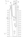
- 4 is a side view for explaining attachment of a semiconductor device mounted on a circuit board to a heat dissipation fin in the first embodiment.
- FIG. 1 is a side view showing a state in which a semiconductor device mounted on a circuit board and heat dissipation fins are attached in a first embodiment
- FIG. 11 is a top view of a semiconductor device according to a second embodiment.
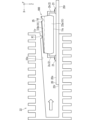
- 13 is a side view for explaining attachment of a semiconductor device mounted on a circuit board to a heat dissipation fin in a second embodiment.
- FIG. 13 is a top view of a semiconductor device according to a first modification of the second embodiment;
- FIG. 13 is a top view of a semiconductor device according to a second modification of the second embodiment.
- FIG. 13 is a top view of a semiconductor device according to a third modification of the second embodiment.
- FIG. 13 is a front view of a semiconductor device according to a fourth modification of the second embodiment;
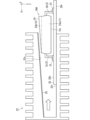
- 13 is a side view for explaining attachment of a semiconductor device mounted on a circuit board to a heat dissipation fin in a third embodiment.
- FIG. 13A to 13C are diagrams for explaining the shape of an insulating material formed on a heat dissipation fin in the third embodiment.
- FIG. 13 is a block diagram showing a configuration of a power conversion system to which a power conversion device according to a fourth embodiment is applied.
- FIG. 1A and 1B are diagrams for explaining attachment of a semiconductor device mounted on a circuit board to heat dissipation fins in a related art.
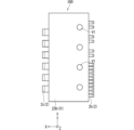
- Fig. 1 is a top view of a semiconductor device 100 according to the first embodiment.
- Fig. 2 is a cross-sectional view taken along line AA in Fig. 1.
- the X direction, Y direction, and Z direction are mutually orthogonal.
- the X direction, Y direction, and Z direction shown in the following figures are also mutually orthogonal.
- the direction including the X direction and the -X direction, which is the opposite direction of the X direction is also referred to as the "X-axis direction”.
- the direction including the Y direction and the -Y direction, which is the opposite direction of the Y direction is also referred to as the "Y-axis direction”.
- the direction including the Z direction and the -Z direction, which is the opposite direction of the Z direction is also referred to as the "Z-axis direction”.
- the semiconductor device 100 includes a lead frame 2, a semiconductor element 3p, a control semiconductor element 3i, an insulating layer 9, a heat sink 10, and a sealing material 11.
- the lead frame 2 includes a die pad 2a, a power lead 2c (first lead), a control lead 2b (second lead), and a suspension lead 2n.
- the die pad 2a is formed in a plate shape. When viewed from the Z direction, the die pad 2a is formed in a rectangular shape.
- the die pad 2a has one side, 2s, and the other side, 2r.
- the side 2r is the side of the die pad 2a opposite to the side 2s.
- the sides 2s and 2r are flat surfaces.
- the die pad 2a is connected to the power lead 2c via the suspension lead 2n.
- the control lead 2b is arranged on the opposite side of the die pad 2a to the power lead 2c. Specifically, the power lead 2c is arranged in the X direction relative to the die pad 2a, and the control lead 2b is arranged in the -X direction relative to the die pad 2a.
- the semiconductor element 3p is, for example, a power semiconductor element that operates at a high voltage. Note that the semiconductor element 3p is not limited to a power semiconductor element, and may be, for example, a semiconductor element that operates at a low voltage.
- a semiconductor element 3p is mounted on the surface 2s of the die pad 2a. Specifically, the semiconductor element 3p is bonded to the surface 2s of the die pad 2a by a bonding material 4.
- the bonding material 4 is, for example, solder.
- a control semiconductor element 3i is bonded to the Z-direction surface of the control lead 2b by a bonding material 8.
- the bonding material 8 is, for example, solder.
- the wires 7s are connected to the control semiconductor element 3i.
- the wires 7s are signal transmission wires.
- the semiconductor element 3p and the control semiconductor element 3i are electrically connected by a wire 7s.
- the control semiconductor element 3i and the control lead 2b are electrically connected by a wire 7s.
- the semiconductor element 3p is electrically connected to the power lead 2c by a wire 7p.
- a heat sink 10 is disposed on face 2r of die pad 2a via an insulating layer 9.
- Heat sink 10 has one face, face 10s, and the other face, face 10r.
- Face 10r is the face of heat sink 10 opposite face 10s.
- the insulating layer 9 is disposed between the die pad 2a and the heat sink 10.
- the insulating layer 9 is in contact with the surface 2r of the die pad 2a and the surface 10s of the heat sink 10.
- the sealing material 11 is, for example, a molded resin.
- the sealing material 11 seals the semiconductor element 3p, the control semiconductor element 3i, the wires 7p, 7s, the die pad 2a, the suspension lead 2n, the power lead 2c, the insulating layer 9, and the heat sink 10, with the tip (the other end) of the control lead 2b and the tip (the other end) of the power lead 2c exposed.
- the sealing material 11 has a surface 11s and a surface 11r.
- Surface 11s is the surface of the sealing material 11 facing the Z direction.
- Surface 11r is the surface of the sealing material 11 opposite surface 11s, facing the -Z direction.
- the control lead 2b protrudes in the -X direction from the -X side of the sealing material 11.
- the control lead 2b is bent so that the tip of the control lead 2b that is outside the sealing material 11 is parallel to the Z direction, and is then bent again so that it is parallel to the X direction.
- the power lead 2c protrudes in the X direction from the side of the sealing material 11 in the X direction.
- the control lead 2b is bent so that the tip of the control lead 2b that is outside the sealing material 11 is parallel to the Z direction, and is then bent again so that it is parallel to the X direction.
- each part will be specifically described.
- copper (Cu) or aluminum (Al) is used as the material for the lead frame 2.
- an alloy composed of copper (Cu) and aluminum (Al) may be used as the material for the lead frame 2.
- the surface of the lead frame 2 may be plated with nickel (Ni), silver (Ag), or gold (Au) to prevent oxidation. That is, a nickel plating film, a silver plating film, or a gold plating film may be formed on the surface of the lead frame 2. The plating film may be formed partially on the lead frame 2.
- the area on which the plating film is formed is also referred to as the "area to be plated.”
- the area to be plated is an area that is susceptible to the effects of surface oxidation.
- the area to be plated is, for example, the periphery of the area on the surface 2s of the die pad 2a where the semiconductor element 3p is bonded by the bonding material 4.
- the area to be plated is, for example, the periphery of the area on the Z-direction surface of the control lead 2b where the control semiconductor element 3i is bonded by the bonding material 8.
- the area to be plated is, for example, the area around the area of the Z-direction surface of the control lead 2b where the wire 7s is connected.
- the area to be plated is, for example, the area around the area of the Z-direction surface of the power lead 2c where the wire 7p is connected.
- the semiconductor element 3p is an element that functions, for example, as a switching element or a rectifying element.
- the switching element is, for example, an IGBT (Insulated Gate Bipolar Transistor) or a MOSFET (Metal-Oxide-Semiconductor Field-Effect Transistor).
- the rectifying element is a diode element.
- the material constituting the semiconductor element 3p is, for example, silicon (Si).
- the material constituting the semiconductor element 3p is not limited to silicon, and may be, for example, a wide bandgap semiconductor material such as silicon carbide (SiC), gallium nitride (GaN), or diamond (C).
- a wide bandgap semiconductor material is a material that has a bandgap wider than that of silicon.
- the semiconductor element 3p made of a wide bandgap semiconductor material is capable of operating using a large current and in a high-temperature environment. For this reason, it is preferable that the material constituting the semiconductor element 3p is a wide bandgap semiconductor material.
- a semiconductor device 100 equipped with such electronic components is known as an IPM (Intelligent Power Module).
- the material constituting the wires 7p and 7s may be aluminum (Al), copper (Cu), gold (Au), silver (Ag), or the like.
- the material constituting the wires 7p and 7s may also be an alloy.
- An alloy is composed of two or more metals selected from the metals aluminum (Al), copper (Cu), gold (Au), and silver (Ag).
- the material constituting the wires 7p and 7s may also be an alloy to which a metal element such as nickel (Ni) or iron (Fe) has been added.
- the shape of the wires 7p and 7s is, for example, a thin wire or a cylindrical shape.
- the cross-sectional shape of the wires 7p and 7s is, for example, a circle.
- the diameter of the circle is, for example, 10 ⁇ m or more and 500 ⁇ m or less.
- Wires 7p and 7s are bonded in a wire bonding process by existing methods such as ball bonding or wedge bonding. If the material constituting wire 7p is the same as the material constituting wire 7s, wires 7p and 7s can be bonded in the same wire bonding process.
- wire 7p is the main wiring. Therefore, the thickness of wire 7p is thicker than wire 7s. Note that the thickness of wire 7p may be the same as that of wire 7i. Also, the thickness of wire 7p may be thinner than that of wire 7s.
- the thickness of the wire 7p is the same as the thickness of the wire 7s.
- the thickness of the wire 7p may be the same as the thickness of the wire 7s.
- the sealing material 11 may also be a composite material.
- the composite material is a material that contains, for example, a filler or other filler and a resin as main components.
- the filler is used to adjust the thermal expansion coefficient or mechanical properties of the sealing material 11.
- the resin contained in the composite material is, for example, a thermosetting resin with high electrical resistivity, such as an epoxy resin. It is preferable that the sealing material 11 has high insulation properties, good moldability, and reliability.
- the sealing material 11 is formed, for example, by a transfer molding method.
- the sealing material 11 seals a part of the lead frame 2 so that the tip (other end) of the power lead 2c and the tip (other end) of the control lead 2b are exposed from the sealing material 11.
- the sealing material 11 also seals the semiconductor element 3p, the control semiconductor element 3i, the wires 7p, 7s, the die pad 2a, the suspension lead 2n, the power lead 2c, the insulating layer 9, and the heat sink 10.
- the tip of the power lead 2c and the tip of the control lead 2b exposed from the sealing material 11 are electrically connected to the circuit board 20 (see FIG. 3) and other devices.
- the sealing material 11 is provided with a first inclined portion 23b, the details of which will be described later.
- the material constituting the insulating layer 9 is a material with high heat dissipation and insulation properties.
- the insulating layer 9 is, for example, a thermally conductive insulating resin sheet.
- the insulating layer 9 is disposed on the surface 2r of the die pad 2a.
- the insulating layer 9 is, for example, a printed sheet, a transferred sheet, or a molded sheet.
- the insulating layer 9 has a rectangular shape when viewed from the Z direction.
- the insulating layer 9 is equal to or smaller than the size of the die pad 2a when viewed from the Z direction.
- the insulating layer 9 may be larger than the size of the die pad 2a when viewed from the Z direction.
- the thickness of the insulating layer 9 is set taking into consideration the heat dissipation properties of the insulating layer 9.
- the thickness of the insulating layer 9 is thinner than the thickness of the die pad 2a. For example, if the thickness of the die pad 2a is in the range of 200 ⁇ m or more and 500 ⁇ m or less, it is preferable that the thickness of the insulating layer 9 is approximately 200 ⁇ m or less.
- the insulating layer 9 may be an insulating substrate consisting of a conductor layer and a ceramic plate.
- the material constituting the conductor layer is a metal such as copper (Cu), aluminum (Al), or nickel (Ni).
- the surface of the conductor layer may be plated with gold (Au), silver (Ag), or nickel (Ni).
- the material constituting the ceramic plate is, for example, a ceramic material or a glass ceramic material.
- the ceramic material is, for example, alumina, silicon nitride, or aluminum nitride.
- a heat sink 10 is placed in contact with the insulating layer 9 to improve the heat dissipation properties of the insulating layer 9.
- the material that constitutes the heat sink 10 is, for example, an alloy.
- the alloy is, for example, aluminum (Al) to which at least one of the metals magnesium (Mg) and manganese (Mn) is added.
- the material constituting the heat sink 10 is not limited to, for example, an alloy, and may be a metal other than an alloy.
- the material constituting the heat sink 10 may be, for example, copper (Cu).
- the heat sink 10 may also be a plate-shaped member made of aluminum (Al).
- the material constituting the heat sink 10 may be a material other than a metal.
- the material constituting the heat sink 10 may be, for example, an inorganic or organic material with high thermal conductivity.
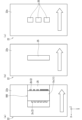
- FIG. 14 is a diagram for explaining the attachment of a semiconductor device 101 mounted on a circuit board 20 and heat dissipation fins 102 according to the related art.
- a bonding material 21 such as solder is printed or applied onto the pattern of the circuit board 20, and then the lead frame 2 is placed on the pattern of the circuit board 20 with the semiconductor device 101 and the circuit board 20 facing each other, and solder bonding is performed using a reflow oven or the like. This allows the semiconductor device 101 to be mounted on the circuit board 20 as shown in FIG. 14.
- the insulating material 25 has the second highest thermal resistance in the heat dissipation path from the semiconductor device 101 to the heat dissipation fins 22, and even if the thermal resistance of the semiconductor device 101 is reduced, the thermal resistance between the insulating material 25 and the heat dissipation fins 22 deteriorates, and the total thermal resistance in the heat dissipation path from the semiconductor device 101 to the heat dissipation fins 22 increases. As a result, the life of the semiconductor element mounted on the semiconductor device 101 is reduced, and even the semiconductor device 101 may be destroyed.
- the first embodiment is made to solve such problems, and the features of the semiconductor device 100 according to the first embodiment will be described in detail below.
- the dimensional variation in the thickness direction of the semiconductor device 101 refers to the dimensional variation in the thickness direction of the sealing material 11, the dimensional variation in the Z-axis direction caused by the bending process of the lead frame 2, the dimensional variation in the thickness direction of the bonding material 21, and the dimensional variation in the Z-axis direction of the heat dissipation fins 22.
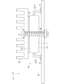
- Figure 3 is a side view for explaining the attachment of the semiconductor device 100 mounted on the circuit board 20 to the heat dissipation fins 22 in the first embodiment.
- a first inclined portion 23b is provided from a region of the sealing material 11 extending along the surface 10r, which is the other surface of the sealing material 11 opposite the surface 10s, which is one surface of the heat sink 10, to the surface 11r, which is the surface of the sealing material 11 on which the heat sink 10 is arranged.
- the sealing material 11 has a main body portion 23a and a first inclined portion 23b.
- the main body portion 23a is a portion represented by a region from the surface 11s of the sealing material 11 to a virtual line extending along the surface 10r of the heat sink 10.
- the first inclined portion 23b is a portion represented by a region from the virtual line extending along the surface 10r of the heat sink 10 to the surface 11r of the sealing material 11.
- the surface represented by the imaginary line extending along the surface 10r of the heat sink 10 is a flat surface.
- the first inclined portion 23b is inclined so that the thickness of the first inclined portion 23b increases from the power lead 2c side (X direction) to the control lead 2b side (-X direction).
- the heat dissipation fins 22 attached to the semiconductor device 100 are U-shaped in side view.
- the heat dissipation fins 22 are attached to the semiconductor device 100 by sandwiching the semiconductor device 100 mounted on one surface 20s of the circuit board 20 between surface 11r, which is the surface on which the heat sink 10 is arranged in the sealing material 11 of the semiconductor device 100, and surface 20r, which is the other surface of the circuit board 20 opposite surface 20s on which the semiconductor device 100 is mounted, via insulating material 25.
- a second inclined portion 22s is provided in the portion of the heat dissipation fin 22 facing the first inclined portion 23b, which is inclined in the same direction as the first inclined portion 23b and has an inclination corresponding to the inclination of the first inclined portion 23b.
- the second inclined portion 22s is inclined in the same direction as the first inclined portion 23b, and has a gentler inclination than the first inclined portion 23b. In this way, an angle difference is provided between the first inclined portion 23b of the sealing material 11 and the second inclined portion 22s of the heat dissipation fin 22. This makes it possible to fix the heat dissipation fin 22 to the semiconductor device 100 without screws, simply by inserting the heat dissipation fin 22 in the X-axis direction from the side of the circuit board 20 on which the semiconductor device 100 is mounted.
- the dimensional variations in the thickness direction of the semiconductor device 100 refer to the dimensional variations in the thickness direction of the sealing material 11, the dimensional variations in the Z-axis direction caused by the bending process of the lead frame 2, the dimensional variations in the thickness direction of the bonding material 21, and the dimensional variations in the Z-axis direction of the heat dissipation fins 22.
- the thickness of the first inclined portion 23b is set to be smaller than the total dimensional variation in the thickness direction of the semiconductor device 100. As a result, the inclination angle of the first inclined portion 23b is reduced, and the insertion distance of the heat dissipation fin 22 is increased. In this way, by increasing the insertion distance of the heat dissipation fin 22, the insertion distance of the heat dissipation fin 22 can be adjusted, so that the dimensional variation in the thickness direction of the semiconductor device 100 can be absorbed and the gap between the sealing material 11 of the semiconductor device 100 and the heat dissipation fin 22 can be adjusted.
- the thickness of the first inclined portion 23b refers to the end of the inclination of the first inclined portion 23b on the end side (the side where the thickness of the first inclined portion 23b becomes thicker), that is, the thickness of the end of the first inclined portion 23b in the -X direction.
- an excessive thickness of the insulating material 25 was required to take into account all dimensional variations in the thickness direction of the semiconductor device 101.
- an insulating material 25 having a minimum thickness is placed between the semiconductor device 100 and the heat dissipation fins 22, so that the semiconductor device 100 and the heat dissipation fins 22 can be sufficiently closely attached to each other.
- the minimum thickness of the insulating material 25 is sufficient to absorb the surface roughness of the sealing material 11 and heat dissipation fins 22 of the semiconductor device 100, and approximately several tens of ⁇ m is sufficient. In other words, the total thermal resistance from the semiconductor device 100 to the heat dissipation fins 22 can be reduced, resulting in high reliability of the semiconductor device 100. In addition, it is possible to reduce the material costs, processing costs, and inspection costs that were incurred to reduce the above-mentioned dimensional variations.
- the first inclined portion 23b is inclined so that the thickness of the first inclined portion 23b increases from the power lead 2c side (X direction) to the control lead 2b side (-X direction), but this is not limited to the above.
- the first inclined portion 23b may be inclined so that the thickness of the first inclined portion 23b increases from the control lead 2b side (-X direction) to the power lead 2c side (X direction).
- the first inclined portion 23b may not be inclined in the X-axis direction, but may be inclined in a direction (Y-axis direction) perpendicular to the direction connecting the power lead 2c and the control lead 2b.
- the first inclined portion 23b may be inclined so that the thickness of the first inclined portion 23b increases from the Y direction to the -Y direction, or from the -Y direction to the Y direction.
- the end point (-X direction) of the inclination of the first inclined portion 23b can be formed at a position away from the die pad 2a on which the semiconductor element 3p, which is the main heat source, is mounted.
- the inclination angle of the first inclined portion 23b may be set according to the size of the circuit board 20, the mounting position of the semiconductor device 100 on the circuit board 20, and the size of the heat dissipation fins 22. If the inclination angle is small, the size of the heat dissipation fins 22 tends to be large in the X-axis direction, and the insertion distance of the heat dissipation fins 22 becomes longer, so that the dimensional variation in the thickness direction of the semiconductor device 100 can be further absorbed.
- the inclination angle of the first inclined portion 23b is a trade-off between the manufacturing cost and the overall size including the semiconductor device 100 and the heat dissipation fins 22.
- the circuit board 20 since the surface 20r of the circuit board 20 and the heat dissipation fins 22 are in contact with each other, the circuit board 20 itself is also cooled, making it possible to increase the pattern current density of the circuit board 20 and improving the degree of freedom in circuit design.
- the thermal resistance of the semiconductor device 100 has tended to decrease due to the evolution of the semiconductor element 3p, the sealing material 11, and the bonding material 4 that contacts the semiconductor element 3p, but the heat may be transferred to the control lead 2b and the power lead 2c in a large amount. Therefore, the heat resistance of the bonding material 21 that bonds the circuit board 20 to the control lead 2b and the power lead 2c may become a bottleneck in improving the performance of the semiconductor device 100.
- the temperature of the control lead 2b and the power lead 2c that connect the semiconductor device 100 to the circuit board 20 can be reduced, which may be one of the means for eliminating the bottleneck in improving the performance of the semiconductor device 100.
- FIG. 4 is a side view showing the state in which the semiconductor device 100 mounted on the circuit board 20 and the heat dissipation fins 22 are attached in the first embodiment. Also, as shown in FIG. 4, the state in which the semiconductor device 100 mounted on the circuit board 20 is inserted into the heat dissipation fins 22 and assembled is called an inverter board.
- the semiconductor device 100 of the first embodiment comprises a lead frame 2 including a die pad 2a, a power lead 2c having one end connected to the die pad 2a, and a control lead 2b arranged on the opposite side of the die pad 2a from the power lead 2c, a semiconductor element 3p mounted on a surface 2s of the die pad 2a, a controlling semiconductor element 3i mounted on a surface in the Z direction at one end side of the control lead 2b and controlling the semiconductor element 3p, a heat sink 10 arranged on a surface 2r of the die pad 2a opposite to the surface 2s of the die pad 2a via an insulating layer 9, with the insulating layer 9 and surface 10s in contact with each other, and a sealing material 11 that seals the semiconductor element 3p, the controlling semiconductor element 3i, the heat sink 10, and the lead frame 2 with the other end side of the power lead 2c and the other end side of the control lead 2b exposed.
- the sealing material 11 has a first inclined portion 23b to which the heat dissipation fins 22 are attached by clamping between a surface 11r of the sealing material 11 of the semiconductor device 100 on which the heat sink 10 is arranged and a surface 20r of the circuit board 20 opposite the surface 20s on which the semiconductor device 100 is mounted, and the first inclined portion 23b is arranged from a region extending along the surface 10r of the sealing material 11 opposite the surface 10s of the heat sink 10 to the surface 11r of the sealing material 11 on which the heat sink 10 is arranged.
- the heat dissipation fins 22 by inserting the heat dissipation fins 22 from the side of the circuit board 20 on which the semiconductor device 100 is mounted, it is possible to attach the semiconductor device 100 and the heat dissipation fins 22 in a state where they are in sufficient contact with each other. As a result, it is possible to make the thickness of the insulating material 25 placed between the semiconductor device 100 and the heat dissipation fins 22 thinner than before. This makes it possible to reduce the thermal resistance from the semiconductor device 100 to the heat dissipation fins 22.
- the heat dissipation fins 22 are inserted from the side of the circuit board 20 on which the semiconductor device 100 is mounted, and the semiconductor device 100 and the heat dissipation fins 22 are fixed together by the first inclined portion 23b of the semiconductor device 100 and the second inclined portion 22s of the heat dissipation fins 22, eliminating the need for a screw fastening process.
- the two screw holes 12 provided in the semiconductor device 101 of the related technology are also unnecessary. As a result, this contributes to the miniaturization of the semiconductor device 100.
- the second inclined portion 22s has a gentler inclination than the first inclined portion 23b.
- the semiconductor device 100 and the heat dissipation fin 22 are fixed when the heat dissipation fin 22 is inserted from the side of the circuit board 20 on which the semiconductor device 100 is mounted. This allows the heat dissipation fin 22 to be attached to the semiconductor device 100 without the need for screws.
- the first inclined portion 23b is inclined so that the thickness of the first inclined portion 23b increases from the power lead 2c side to the control lead 2b side. Therefore, by increasing the thickness of the sealing material 11 on the control lead 2b side, the reliability of the control semiconductor element 3i and the components arranged around it is improved.
- the first inclined portion 23b is inclined so that the thickness of the first inclined portion 23b increases from the control lead 2b side toward the power lead 2c side. Therefore, by increasing the thickness of the sealing material 11 on the power lead 2c side, the reliability of the semiconductor element 3p and the components arranged around it is improved.
- the first inclined portion 23b is inclined in a direction (Y-axis direction) perpendicular to the direction connecting the power lead 2c and the control lead 2b. This improves the reliability of the components arranged around the terminal end in the Y-axis direction.
- the thickness of the first inclined portion 23b is smaller than the total dimensional variation in the thickness direction (Z-axis direction) of the semiconductor device 100. Therefore, the inclination angle of the first inclined portion 23b is smaller, and the insertion distance of the heat dissipation fin 22 is longer. In this way, by increasing the insertion distance of the heat dissipation fin 22, the insertion distance of the heat dissipation fin 22 can be adjusted, so that the dimensional variation in the thickness direction of the semiconductor device 100 can be absorbed and the gap between the sealing material 11 of the semiconductor device 100 and the heat dissipation fin 22 can be adjusted.
- Fig. 5 is a top view of the semiconductor device 100 according to the second embodiment.
- Fig. 6 is a side view for explaining the attachment of the semiconductor device 100 mounted on the circuit board 20 to the heat dissipation fins 22 in the second embodiment. Note that in the second embodiment, the same components as those explained in the first embodiment are given the same reference numerals and the explanation thereof will be omitted.
- a recess V1 is provided in the first inclined portion 23b of the semiconductor device 100, and a protrusion X1 is provided in the second inclined portion 22s of the heat dissipation fin 22.
- the recess V1 is formed in a semicircular shape in a cross-sectional view, and is recessed in the Z direction.
- a plurality of recesses V1 are provided in a direction perpendicular to the direction connecting the power lead 2c and the control lead 2b.
- two recesses V1 are provided at the end of the inclination of the first inclined portion 23b on the side of the end point of the inclination (the side where the thickness of the first inclined portion 23b becomes thicker), i.e., at the end of the first inclined portion 23b in the -X direction, and are spaced apart in the Y axis direction.
- the depth of the recess V1 is formed to be shallower than the thickness of the first inclined portion 23b.
- the protrusion X1 is formed in a semicircular shape in a cross-sectional view and protrudes in the Z direction. Two protrusions X1 are provided at a distance in the Y-axis direction at the end of the inclination of the second inclined portion 22s of the heat dissipation fin 22 on the -X direction side so as to fit into the recess V1. When the heat dissipation fin 22 is inserted from the side of the circuit board 20 on which the semiconductor device 100 is mounted, the protrusion X1 fits into the recess V1, thereby firmly fixing the semiconductor device 100 and the heat dissipation fin 22.
- the protrusion X1 may be formed to match the position of the recess V1, but the position of the protrusion X1 may be shifted slightly toward the start point of the slope of the second inclined portion 22s (X direction) in increments of 1 mm or less.
- the protrusion X1 By shifting the position of the protrusion X1 slightly toward the start point of the slope of the second inclined portion 22s, when the protrusion X1 is fitted into the recess V1, the protrusion X1 is crimped into the recess V1, and the semiconductor device 100 and the heat dissipation fin 22 can be fixed even more firmly.
- the sizes of the recess V1 and the protrusion X1 affect the fixing strength, the sizes may be determined according to the required fixing strength.
- the positions of the depression V1 and the protrusion X1 only need to be at the end of the slope of the first sloped portion 23b and the end of the slope of the second sloped portion 22s, respectively, and are changed according to the slope directions of the first sloped portion 23b and the second sloped portion 22s, respectively.
- the thicker end of the first inclined portion 23b is provided with a recess V1 into which the protrusion X1 provided on the second inclined portion 22s of the heat dissipation fin 22 can be fitted. Therefore, when the heat dissipation fin 22 is inserted from the side surface of the circuit board 20 on which the semiconductor device 100 is mounted, the protrusion X1 fits into the recess V1, thereby firmly fixing the semiconductor device 100 and the heat dissipation fin 22 together.
- multiple recesses V1 are provided in a direction perpendicular to the direction connecting the power lead 2c and the control lead 2b. Therefore, the semiconductor device 100 and the heat dissipation fins 22 can be fixed more firmly than if there was only one recess V1.
- Fig. 7 is a top view of the semiconductor device 100 according to a first modification of the second embodiment.
- Fig. 8 is a top view of the semiconductor device 100 according to a second modification of the second embodiment.
- Fig. 9 is a top view of the semiconductor device 100 according to a third modification of the second embodiment.
- Fig. 10 is a front view of the semiconductor device 100 according to a fourth modification of the second embodiment.
- three or more recesses V1 may be provided at intervals in the Y-axis direction on the end point side of the inclination of the first inclined portion 23b.
- three or more protrusions X1 are also provided on the second inclined portion 22s of the heat dissipation fin 22 to match the position of the recesses V1. This allows the semiconductor device 100 and the heat dissipation fin 22 to be fixed more firmly than when there are two recesses V1.
- the number of recesses V1 should be determined taking into consideration the required fixing strength.
- the recess V1 may be formed linearly in a direction perpendicular to the direction connecting the power lead 2c and the control lead 2b, i.e., in the Y-axis direction.
- the semiconductor device 100 and the heat dissipation fin 22 can be fixed more firmly than in the case of FIG. 7, and processing costs can also be reduced.
- a linear protrusion X1 is also provided on the second inclined portion 22s of the heat dissipation fin 22 in accordance with the position of the recess V1.
- multiple recesses V1 may be provided in the direction from the power lead 2c to the control lead 2b, i.e., in the X-axis direction.
- multiple recesses V1 may be formed in a direction parallel to the insertion direction of the heat dissipation fin 22, it becomes easier to adjust the fitting position between the recesses V1 and the protrusions X1.
- multiple protrusions X1 are also provided on the second inclined portion 22s of the heat dissipation fin 22 to match the position of the recesses V1.
- the shape of the recess V1 and the protrusion X1 is not limited to a semicircular shape in cross section, but may be, for example, a square, triangular, or diamond shape in cross section.
- the recess V1 may be formed in a sawtooth shape in the direction from the power lead 2c to the control lead 2b, i.e., in the X-axis direction.
- the recess V1 in a sawtooth shape, it becomes easier to adjust the fitting position between the recess V1 and the protrusion X1, and the semiconductor device 100 and the heat dissipation fin 22 can be fixed more firmly.
- a sawtooth-shaped protrusion X1 is also provided on the second inclined portion 22s of the heat dissipation fin 22 in accordance with the position of the recess V1.
- Fig. 11 is a side view for explaining the attachment of the semiconductor device 100 mounted on the circuit board 20 to the heat dissipation fins 22 in the third embodiment.
- Figs. 12(a) to 12(c) are diagrams for explaining the shape of the insulating material 25 formed on the heat dissipation fins 22 in the third embodiment, and the arrows shown in the figures indicate the insertion direction of the semiconductor device 100.
- the same components as those explained in the first and second embodiments are given the same reference numerals and the explanations are omitted.
- the semiconductor device 100 is attached to the heat dissipation fin 22 by forming an insulating material 25 on the surface 11r of the sealing material 11 in the semiconductor device 100, but as shown in FIG. 11, it is also possible to form the insulating material 25 on the second inclined portion 22s of the heat dissipation fin 22, which is the portion of the heat dissipation fin 22 that faces the surface 11r of the sealing material 11.
- the insulating material 25 may also be formed on the protrusion X1.
- the semiconductor device 100 and the heat dissipation fins 22 can be reliably contacted without any gaps via the insulating material 25. This reduces the total thermal resistance from the semiconductor device 100 to the heat dissipation fins 22, resulting in high reliability for the semiconductor device 100.
- the insulating material 25 may have an area larger than that of the semiconductor device 100 when viewed from the surface 11s side opposite to the surface 11r of the sealing material 11 (when viewed from the Z direction). Or, as shown in FIG. 12(b), the insulating material 25 may be formed at a position where the second inclined portion 22s and the semiconductor device 100 start to contact each other, and the insulating material 25 may be spread over the entire surface 11r of the sealing material 11 when the semiconductor device 100 is slid.
- the insulating material 25 has an area smaller than that of the semiconductor device 100 when viewed from the surface 11s side opposite to the surface 11r of the sealing material 11 (when viewed from the Z direction), and is formed linearly in a direction perpendicular to the direction connecting the power lead 2c and the control lead 2b, i.e., in the Y-axis direction.
- the shape of the insulating material 25 is not limited to a square shape, and may be, for example, a circle, a triangle, or a diamond shape. Furthermore, as shown in FIG. 12(c), in order to make it easier for the insulating material 25 to spread over the entire surface 11r of the sealing material 11, multiple pieces of the insulating material 25 may be formed in a direction perpendicular to the direction connecting the power lead 2c and the control lead 2b, i.e., in the Y-axis direction. As a result, it is possible to further reduce the amount of insulating material 25 used compared to the case of FIG. 12(b).
- the semiconductor device 100 according to the above-mentioned first to third embodiments is applied to a power conversion device 200.
- the application of the semiconductor device 100 according to the first to third embodiments is not limited to a specific power conversion device, hereinafter, as a fourth embodiment, a case where the semiconductor device 100 according to the first to third embodiments is applied to a three-phase inverter will be described.
- FIG. 13 is a block diagram showing the configuration of a power conversion system that uses a power conversion device 200 according to embodiment 4.
- the power conversion system shown in FIG. 13 is composed of a power source 400, a power conversion device 200, and a load 300.
- the power source 400 is a DC power source and supplies DC power to the power conversion device 200.
- the power source 400 can be composed of various things, for example, a DC system, a solar cell, or a storage battery, or it may be composed of a rectifier circuit connected to an AC system or an AC/DC converter.
- the power source 400 may also be composed of a DC/DC converter that converts the DC power output from the DC system into a specified power.
- the power conversion device 200 is a three-phase inverter connected between the power source 400 and the load 300, converts the DC power supplied from the power source 400 into AC power, and supplies the AC power to the load 300. As shown in FIG. 13, the power conversion device 200 includes a main conversion circuit 201 that converts the DC power into AC power and outputs it, and a control circuit 203 that outputs a control signal to the main conversion circuit 201 to control the main conversion circuit 201.
- the load 300 is a three-phase motor that is driven by AC power supplied from the power conversion device 200.
- the load 300 is not limited to a specific use, but is a motor mounted on various electrical devices, and is used, for example, as a motor for hybrid cars, electric cars, railroad cars, elevators, or air conditioning equipment.
- the power conversion device 200 will be described in detail below.
- the main conversion circuit 201 includes a switching element (not shown) and a freewheeling diode (not shown), and by switching the switching element, the DC power supplied from the power source 400 is converted into AC power and supplied to the load 300.
- the main conversion circuit 201 in this embodiment is a two-level three-phase full bridge circuit, and can be configured from six switching elements and six freewheeling diodes connected in inverse parallel to each switching element.
- At least one of the switching elements and free wheel diodes of the main conversion circuit 201 is configured with a semiconductor device 100 corresponding to any one of the above-mentioned embodiments 1 to 3.
- the main conversion circuit 201 is equipped with the semiconductor device 100 according to embodiment 1.
- the six switching elements are connected in series with two switching elements to configure upper and lower arms, and each upper and lower arm configures each phase (U phase, V phase, W phase) of the full bridge circuit.
- the output terminals of each upper and lower arm, i.e. the three output terminals of the main conversion circuit 201, are connected to the load 300.
- the main conversion circuit 201 also includes a drive circuit (not shown) for driving each switching element, but the drive circuit may be built into the semiconductor device 100, or the semiconductor device 100 may be configured to include a drive circuit separately.
- the drive circuit generates drive signals for driving the switching elements of the main conversion circuit 201, and supplies them to the control electrodes of the switching elements of the main conversion circuit 201. Specifically, in accordance with a control signal from the control circuit 203 (described later), a drive signal for turning the switching element on and a drive signal for turning the switching element off are output to the control electrodes of each switching element.
- the drive signal When the switching element is to be maintained in the on state, the drive signal is a voltage signal (on signal) equal to or higher than the threshold voltage of the switching element, and when the switching element is to be maintained in the off state, the drive signal is a voltage signal (off signal) equal to or lower than the threshold voltage of the switching element.
- the control circuit 203 controls the switching elements of the main conversion circuit 201 so that the desired power is supplied to the load 300. Specifically, it calculates the time (on time) that each switching element of the main conversion circuit 201 should be in the on state based on the power to be supplied to the load 300.
- the main conversion circuit 201 can be controlled by PWM control, which modulates the on time of the switching elements according to the voltage to be output. Then, it outputs a control command (control signal) to a drive circuit provided in the main conversion circuit 201 so that an on signal is output to the switching element that should be in the on state at each point in time, and an off signal is output to the switching element that should be in the off state.
- the drive circuit outputs an on signal or an off signal as a drive signal to the control electrode of each switching element according to this control signal.
- the semiconductor device 100 is used as the switching element and free wheel diode of the main conversion circuit 201, which makes it possible to achieve miniaturization, improved durability, and improved yield.
- the semiconductor device 100 according to the first to third embodiments is applied to a two-level three-phase inverter, but the application of the semiconductor device 100 according to the first to third embodiments is not limited to this, and the semiconductor device 100 can be applied to various power conversion devices.
- a two-level power conversion device is used, but a three-level or multi-level power conversion device may also be used, and when supplying power to a single-phase load, the semiconductor device 100 according to the first to third embodiments may be applied to a single-phase inverter.
- the semiconductor device 100 according to the first to third embodiments can also be applied to a DC/DC converter or an AC/DC converter.
- the power conversion device 200 to which the semiconductor device 100 according to the first to third embodiments is applied is not limited to the case where the load described above is an electric motor, but can also be used, for example, as a power supply device for an electric discharge machine, a laser processing machine, an induction heating cooker, or a non-contact power supply system, and can also be used as a power conditioner for a solar power generation system, a power storage system, etc.
- each embodiment can be freely combined, modified, or omitted as appropriate.
- a second inclined portion is provided at a portion of the heat dissipation fin facing the first inclined portion, the second inclined portion being inclined in the same direction as the first inclined portion and having an inclination corresponding to an inclination of the first inclined portion; 6.
- an end portion of the first inclined portion on the side where the thickness is greater is provided with a recess into which a protrusion provided on the second inclined portion of the heat dissipation fin can be fitted.
- a power conversion device comprising:
- An inverter board including a semiconductor device mounted on one surface of a circuit board includes: a lead frame including a die pad, a first lead having one end connected to the die pad, and a second lead disposed on an opposite side of the die pad from the first lead; a semiconductor element mounted on one surface of the die pad; a control semiconductor element mounted on one surface at one end side of the second lead and controlling the semiconductor element; a heat sink disposed on another surface of the die pad opposite to the one surface via an insulating layer, the one surface being in contact with the insulating layer; a sealing material that seals the semiconductor element, the control semiconductor element, the heat sink, and the lead frame in a state in which the other end side of the first lead and the other end side of the second lead are exposed, a heat dissipation fin is provided that is attached to the semiconductor device by clamping one surface of the sealing material of the semiconductor device on a side where the heat sink is arranged and another surface of the circuit board opposite to the one surface on which the
- Appendix 14 An inverter board as described in Appendix 12 or Appendix 13, wherein the first inclined portion has a recess at an end on the side where the thickness becomes thicker, and the second inclined portion of the heat dissipation fin has a protrusion that can fit into the recess.
- Appendix 16 The inverter board described in Appendix 14, wherein the protrusion is formed linearly in a direction perpendicular to a direction connecting the first lead and the second lead.
- a lead frame including a die pad, a first lead having one end connected to the die pad, and a second lead disposed on an opposite side of the die pad from the first lead; a semiconductor element mounted on one surface of the die pad; a control semiconductor element mounted on one surface at one end side of the second lead and controlling the semiconductor element; a heat sink disposed on another surface of the die pad opposite to the one surface via an insulating layer, the one surface being in contact with the insulating layer; a heat dissipation fin attached to a semiconductor device including a semiconductor element, a control semiconductor element, a heat sink, and a sealing material that seals the lead frame in a state in which the other end side of the first lead and the other end side of the second lead are exposed, A heat dissipation fin is attached to the semiconductor device mounted on one side of a circuit board by clamping one side of the sealing material of the semiconductor device on which the heat sink is arranged and the other side of the circuit board opposite the one side on which the semiconductor device is mounted
- Appendix 21 A heat dissipation fin as described in Appendix 20, wherein the insulating material formed on the heat dissipation fin has an area larger than that of the semiconductor device when viewed from the other side opposite to the one side of the sealing material.
- Appendix 22 A heat dissipation fin as described in Appendix 20, wherein the insulating material formed on the heat dissipation fin has an area smaller than that of the semiconductor device when viewed from the other side opposite the one side of the sealing material, and is formed in a linear shape in a direction perpendicular to the direction connecting the first lead and the second lead.
Landscapes
- Physics & Mathematics (AREA)
- Thermal Sciences (AREA)
- Engineering & Computer Science (AREA)
- Microelectronics & Electronic Packaging (AREA)
- Cooling Or The Like Of Semiconductors Or Solid State Devices (AREA)
Priority Applications (1)
| Application Number | Priority Date | Filing Date | Title |
|---|---|---|---|
| JP2025511004A JPWO2024204310A1 (https=) | 2023-03-31 | 2024-03-27 |
Applications Claiming Priority (2)
| Application Number | Priority Date | Filing Date | Title |
|---|---|---|---|
| JP2023057288 | 2023-03-31 | ||
| JP2023-057288 | 2023-03-31 |
Publications (1)
| Publication Number | Publication Date |
|---|---|
| WO2024204310A1 true WO2024204310A1 (ja) | 2024-10-03 |
Family
ID=92906548
Family Applications (1)
| Application Number | Title | Priority Date | Filing Date |
|---|---|---|---|
| PCT/JP2024/012183 Ceased WO2024204310A1 (ja) | 2023-03-31 | 2024-03-27 | 半導体装置、電力変換装置、インバータ基板、および放熱フィン |
Country Status (2)
| Country | Link |
|---|---|
| JP (1) | JPWO2024204310A1 (https=) |
| WO (1) | WO2024204310A1 (https=) |
Citations (4)
| Publication number | Priority date | Publication date | Assignee | Title |
|---|---|---|---|---|
| JPH0463464A (ja) * | 1990-07-03 | 1992-02-28 | Mitsubishi Electric Corp | 半導体装置 |
| JP2008198835A (ja) * | 2007-02-14 | 2008-08-28 | Nippo Ltd | 放熱装置 |
| WO2015115026A1 (ja) * | 2014-01-30 | 2015-08-06 | パナソニックIpマネジメント株式会社 | 半導体装置及び半導体パッケージ |
| US20180108601A1 (en) * | 2016-10-16 | 2018-04-19 | Alpha And Omega Semiconductor (Cayman) Ltd. | Molded intelligent power module and method of making the same |
Family Cites Families (9)
| Publication number | Priority date | Publication date | Assignee | Title |
|---|---|---|---|---|
| JPS56112945U (https=) * | 1980-01-31 | 1981-08-31 | ||
| JP3070457B2 (ja) * | 1995-11-13 | 2000-07-31 | 富士通電装株式会社 | 半導体の取付装置 |
| DE10326458B4 (de) * | 2003-06-12 | 2006-05-04 | Phoenix Contact Gmbh & Co. Kg | Kühlanordnung für elektronische Bauelemente |
| US7501727B2 (en) * | 2004-08-26 | 2009-03-10 | Mitsubishi Denki Kabushiki Kaisha | Alternator voltage control apparatus |
| JP4998249B2 (ja) * | 2007-12-21 | 2012-08-15 | 住友電気工業株式会社 | 光トランシーバの放熱装置 |
| JP6195019B2 (ja) * | 2014-05-12 | 2017-09-13 | 三菱電機株式会社 | 電力用半導体装置及びその製造方法 |
| JP6233232B2 (ja) * | 2014-07-31 | 2017-11-22 | トヨタ自動車株式会社 | 電力変換装置 |
| JP6223520B1 (ja) * | 2016-09-02 | 2017-11-01 | 三菱電機株式会社 | 電力変換装置 |
| TWI841603B (zh) * | 2018-09-27 | 2024-05-11 | 德商漢高股份有限及兩合公司 | 用於熱介面之耐磨塗層 |
-
2024
- 2024-03-27 WO PCT/JP2024/012183 patent/WO2024204310A1/ja not_active Ceased
- 2024-03-27 JP JP2025511004A patent/JPWO2024204310A1/ja active Pending
Patent Citations (4)
| Publication number | Priority date | Publication date | Assignee | Title |
|---|---|---|---|---|
| JPH0463464A (ja) * | 1990-07-03 | 1992-02-28 | Mitsubishi Electric Corp | 半導体装置 |
| JP2008198835A (ja) * | 2007-02-14 | 2008-08-28 | Nippo Ltd | 放熱装置 |
| WO2015115026A1 (ja) * | 2014-01-30 | 2015-08-06 | パナソニックIpマネジメント株式会社 | 半導体装置及び半導体パッケージ |
| US20180108601A1 (en) * | 2016-10-16 | 2018-04-19 | Alpha And Omega Semiconductor (Cayman) Ltd. | Molded intelligent power module and method of making the same |
Also Published As
| Publication number | Publication date |
|---|---|
| JPWO2024204310A1 (https=) | 2024-10-03 |
Similar Documents
| Publication | Publication Date | Title |
|---|---|---|
| JP7597834B2 (ja) | 少なくとも3つの電力ユニットを備えた電力モジュール | |
| US11139278B2 (en) | Low parasitic inductance power module and double-faced heat-dissipation low parasitic inductance power module | |
| CN112864113B (zh) | 功率器件、功率器件组件与相关装置 | |
| JP7196815B2 (ja) | 半導体モジュール及び電力変換装置 | |
| CN109727960B (zh) | 半导体模块、其制造方法以及电力变换装置 | |
| JP7199167B2 (ja) | パワー半導体モジュール、電力変換装置、およびパワー半導体モジュールの製造方法 | |
| JP6952889B2 (ja) | パワー半導体モジュール及びその製造方法並びに電力変換装置 | |
| JP7561677B2 (ja) | 電力半導体装置、電力半導体装置の製造方法及び電力変換装置 | |
| JP2010097967A (ja) | 半導体装置 | |
| US20240395678A1 (en) | Semiconductor device, method of manufacturing semiconductor device, and power conversion device | |
| US11990393B2 (en) | Semiconductor device including resin with a filler for encapsulating bridge member connected to a substrate | |
| CN215008199U (zh) | 功率器件、功率器件组件、电能转换装置及电能转换设备 | |
| JP3673776B2 (ja) | 半導体モジュール及び電力変換装置 | |
| JP7710605B2 (ja) | パワーモジュールおよび電力変換装置 | |
| US20240030087A1 (en) | Semiconductor device, method of manufacturing semiconductor device, and power conversion device | |
| JPWO2020148879A1 (ja) | 半導体装置、半導体装置の製造方法及び電力変換装置 | |
| CN114730748A (zh) | 用于消耗装置的可控电功率供应的具有被封装的功率半导体的功率模块及用于生产该功率模块的方法 | |
| JP3829641B2 (ja) | パワー半導体モジュール | |
| WO2024204310A1 (ja) | 半導体装置、電力変換装置、インバータ基板、および放熱フィン | |
| WO2025109919A1 (ja) | 半導体装置および電力変換装置 | |
| CN219553614U (zh) | 一种半导体电路和散热器 | |
| US20260052989A1 (en) | Mechanisms for dual coupling a semiconductor package assembly to a component | |
| US20250014972A1 (en) | Package with clip directly connected to oblong electric connection element extending along mounting base | |
| US20250054830A1 (en) | Semiconductor module, power semiconductor device, method for manufacturing semiconductor module, method for manufacturing power semiconductor device, and power conversion device | |
| WO2025089206A1 (ja) | 電力変換装置 |
Legal Events
| Date | Code | Title | Description |
|---|---|---|---|
| 121 | Ep: the epo has been informed by wipo that ep was designated in this application |
Ref document number: 24780416 Country of ref document: EP Kind code of ref document: A1 |
|
| WWE | Wipo information: entry into national phase |
Ref document number: 2025511004 Country of ref document: JP |
|
| NENP | Non-entry into the national phase |
Ref country code: DE |
|
| 122 | Ep: pct application non-entry in european phase |
Ref document number: 24780416 Country of ref document: EP Kind code of ref document: A1 |