WO2024203239A1 - 電子部品及びこれを搭載した電子機器 - Google Patents
電子部品及びこれを搭載した電子機器 Download PDFInfo
- Publication number
- WO2024203239A1 WO2024203239A1 PCT/JP2024/009393 JP2024009393W WO2024203239A1 WO 2024203239 A1 WO2024203239 A1 WO 2024203239A1 JP 2024009393 W JP2024009393 W JP 2024009393W WO 2024203239 A1 WO2024203239 A1 WO 2024203239A1
- Authority
- WO
- WIPO (PCT)
- Prior art keywords
- lead frame
- plating layer
- electronic component
- mold
- resin mold
- Prior art date
- Legal status (The legal status is an assumption and is not a legal conclusion. Google has not performed a legal analysis and makes no representation as to the accuracy of the status listed.)
- Ceased
Links
Images


Classifications
-
- H—ELECTRICITY
- H01—ELECTRIC ELEMENTS
- H01C—RESISTORS
- H01C7/00—Non-adjustable resistors formed as one or more layers or coatings; Non-adjustable resistors made from powdered conducting material or powdered semi-conducting material with or without insulating material
- H01C7/10—Non-adjustable resistors formed as one or more layers or coatings; Non-adjustable resistors made from powdered conducting material or powdered semi-conducting material with or without insulating material voltage responsive, i.e. varistors
-
- H—ELECTRICITY
- H01—ELECTRIC ELEMENTS
- H01G—CAPACITORS; CAPACITORS, RECTIFIERS, DETECTORS, SWITCHING DEVICES, LIGHT-SENSITIVE OR TEMPERATURE-SENSITIVE DEVICES OF THE ELECTROLYTIC TYPE
- H01G4/00—Fixed capacitors; Processes of their manufacture
- H01G4/002—Details
- H01G4/228—Terminals
-
- H—ELECTRICITY
- H01—ELECTRIC ELEMENTS
- H01G—CAPACITORS; CAPACITORS, RECTIFIERS, DETECTORS, SWITCHING DEVICES, LIGHT-SENSITIVE OR TEMPERATURE-SENSITIVE DEVICES OF THE ELECTROLYTIC TYPE
- H01G9/00—Electrolytic capacitors, rectifiers, detectors, switching devices, light-sensitive or temperature-sensitive devices; Processes of their manufacture
- H01G9/004—Details
- H01G9/008—Terminals
- H01G9/012—Terminals specially adapted for solid capacitors
-
- H—ELECTRICITY
- H01—ELECTRIC ELEMENTS
- H01G—CAPACITORS; CAPACITORS, RECTIFIERS, DETECTORS, SWITCHING DEVICES, LIGHT-SENSITIVE OR TEMPERATURE-SENSITIVE DEVICES OF THE ELECTROLYTIC TYPE
- H01G9/00—Electrolytic capacitors, rectifiers, detectors, switching devices, light-sensitive or temperature-sensitive devices; Processes of their manufacture
- H01G9/004—Details
- H01G9/08—Housing; Encapsulation
- H01G9/10—Sealing, e.g. of lead-in wires
Definitions
- This disclosure relates to electronic components and electronic devices incorporating the electronic components, and more specifically to electronic components including an electronic element, a lead frame, and a resin mold, and electronic devices incorporating the electronic components.
- electronic elements such as laminated varistors are covered with a resin mold to improve reliability such as moisture resistance, and lead frames are used that extend outside from the resin mold to enable surface mounting on circuit boards.
- Patent Document 1 discloses a multilayer ceramic component that has external electrodes formed on the surfaces of the laminate in a multilayer varistor, and after a lead frame is connected to the external electrodes with a conductive adhesive, the entire peripheral surface of the laminate is covered with a molded resin.
- Patent Document 1 during the heat treatment of reflow mounting, the metal that constitutes the plating layer of the lead frame melts, and due to the expansion of the molded resin and the lead frame, it is expelled to a location where the lead frame is exposed to the outside from the molded resin, and the expelled metal may become spherical or have an irregular shape.
- the metal of the plating layer of the lead frame becomes irregular, it falls off due to its low adhesion, and there is a risk of causing a short circuit on the mounting board.
- the objective of this disclosure is to provide an electronic component that can suppress deformation of the metal in the plating layer of a lead frame, and an electronic device equipped with this electronic component.
- the electronic component includes an electronic element, a lead frame, and a resin mold.
- the lead frame has a base material and a plating layer provided on the surface of the base material, has a first surface and a second surface opposite to the first surface, and is electrically connected to the electronic element.
- the resin mold includes a first mold portion and a second mold portion. The first mold portion covers the electronic element and a part of the lead frame, and is in contact with the first surface of the lead frame. The second mold portion is in contact with the second surface of the lead frame.
- the lead frame includes a first portion covered by the resin mold, a second portion that protrudes outward from a side surface of the resin mold and extends in a planar shape with the first surface not covered by the first mold portion and the second surface covered by the second mold portion, and a third portion that bends from the second portion and extends along the side surface of the second mold portion so that the second surface faces the side surface of the second mold portion.
- An electronic device is equipped with the electronic component.
- the electronic component disclosed herein and the electronic device incorporating the electronic component can provide an electronic component that can suppress deformation of the metal in the plating layer of the lead frame, and an electronic device incorporating the electronic component.
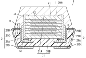
- FIG. 1A is a schematic perspective view showing an example of an electronic component according to an embodiment of the present invention.
- FIG. 1B is a schematic cross-sectional view of the electronic component shown in FIG. 1A of the present embodiment taken along the line MM.
- FIG. 1C is a schematic cross-sectional view of a region R of the electronic component shown in FIG. 1B according to the present embodiment.
- FIG. 2A is a schematic perspective view showing another example of the electronic component according to this embodiment.
- FIG. 2B is a schematic cross-sectional view of another example electronic component according to this embodiment taken along the line NN shown in FIG. 2A.
- FIG. 3A is a schematic perspective view showing another example of the electronic component according to this embodiment.
- FIG. 1A is a schematic perspective view showing an example of an electronic component according to an embodiment of the present invention.
- FIG. 1B is a schematic cross-sectional view of the electronic component shown in FIG. 1A of the present embodiment taken along the line MM.
- FIG. 1C is
- FIG. 3B is a schematic perspective view showing another example of the electronic component according to this embodiment.
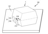
- FIG. 4A is a perspective view of the electronic device of the present embodiment.
- 4B is a schematic cross-sectional view of the electronic device shown in FIG. 4A taken along the line KK in the vicinity of the second portion of the lead frame.
- the "side surface” of a resin mold, etc. means the surface where the lead frame protrudes from the resin mold, etc.
- the “bottom surface” of a resin mold, etc. means the lower surface of the resin mold, etc.
- the inventors in their diligent research into solving the problems they found, discovered that in the conventional electronic components, cracks exist in the plating layer provided on the surface of the substrate when the lead frame is bent at the location where the lead frame is exposed to the outside from the molded resin. They discovered that these cracks prevent the metal of the plating layer of the ejected lead frame from spreading out, causing it to become spherical or otherwise deformed. The inventors further researched the structure of electronic components in order to prevent the metal plating layer of the lead frame from becoming deformed, which is believed to occur in this way, and have completed the present disclosure.
- FIG. 1A is a schematic perspective view showing an example of an electronic component 1 according to this embodiment.
- FIG. 1B is a schematic cross-sectional view of the M-M section of the electronic component 1 shown in FIG. 1A.
- FIG. 2A is a schematic perspective view showing another example of the electronic component 1 according to this embodiment.
- FIG. 2B is a schematic cross-sectional view of the N-N section of the electronic component 1 shown in FIG. 2A.
- the electronic component 1 of this embodiment includes an electronic element 11, a lead frame 21, and a resin mold 31, and the lead frame 21 and the resin mold 31 have the following configuration.
- the lead frame 21 has a base material (hereinafter also referred to as base material (P)) and a plating layer provided on the surface of the base material (P), has a first surface X and a second surface Y opposite the first surface X, and is electrically connected to the electronic element 11.
- base material hereinafter also referred to as base material (P)
- P base material
- plating layer provided on the surface of the base material (P)
- P has a first surface X and a second surface Y opposite the first surface X, and is electrically connected to the electronic element 11.
- the resin mold 31 includes a first molded portion 31A and a second molded portion 31B.
- the first molded portion 31A covers the electronic element 11 and a portion of the lead frame 21, and is in contact with a first surface X of the lead frame 21.
- the second molded portion 31B is in contact with a second surface Y of the lead frame 21.
- the lead frame 21 has a first portion 21A, a second portion 21B, and a third portion 21C.
- the first portion 21A is covered by a resin mold 31.
- the second portion 21B protrudes outward from the side of the resin mold 31 and extends in a flat plane with a first surface X not covered by the first molded portion 31A and a second surface Y covered by the second molded portion 31B.
- the third portion 21C bends from the second portion and extends along the side of the second molded portion 31B so that the second surface Y faces the side of the second molded portion 31B.
- the electronic component 1 of this embodiment by being provided with the above-mentioned configuration, can suppress the metal of the plating layer of the lead frame 21 from becoming deformed.
- the electronic component 1 of this embodiment has a feature not found in conventional electronic components in that the lead frame 21 is provided with the second portion 21B.
- the second portion 21B is a portion that protrudes outward from the side of the resin mold 31, and extends in a planar shape with the first surface X not covered by the first mold portion 31A and the second surface Y covered by the second mold portion 31B.
- the metal that melts in the plating layer of the first portion 21A is discharged from the inside of the resin mold 31 and moves to the portion that extends in a planar shape on the first surface X of the second portion 21B during the heat treatment of the reflow mounting.
- the metal of the migrated plating layer can wet and spread over the area of the second portion 21B that extends in a planar shape.
- the electronic component 1 of this embodiment can prevent the metal of the plating layer of the lead frame 21 from becoming misshapen.
- the electronic component 1 includes an electronic element 11 , a lead frame 21 , and a resin mold 31 .
- the electronic component 1 typically includes one electronic element 11.
- the number of electronic elements 11 is not limited to this, and may be two or more.
- the electronic element 11 may be, for example, a laminated varistor or a solid electrolytic capacitor.
- the electronic element 1 is a laminated varistor 40.
- the laminated varistor 40 typically includes a sintered body 41, a number of internal electrodes 42, and a number of external electrodes 43.
- the electronic element 11 is electrically connected to the lead frame 21.
- This electrical connection can be achieved, for example, by bonding the external electrodes 43 arranged on the side, bottom, etc. of the laminated varistor 40, which is the electronic element 11, to the lead frame 21 using, for example, a conductive adhesive 50, as shown in Figures 1B and 2B.
- the lead frame 21 is a thin, conductive member used to electrically connect the electronic element 11 to a surface on which the electronic component 1 is mounted.
- the lead frame 21 has a thickness of, for example, 0.05 mm or more and 3 mm or less, and a width (a dimension in a direction perpendicular to the length direction) of, for example, 0.5 mm or more and 10 mm or less.
- the electronic component 1 typically has a pair of lead frames 21.
- the number of lead frames 21 is not limited to this, and may be one, or three or more.
- FIG. 1C is a schematic cross-sectional view of region R of the electronic component 1 shown in FIG. 1B.
- the lead frame 21 has a first surface X that contacts the first molded portion 31A of the resin mold 31 and a second surface Y that contacts the second molded portion 31B.
- the lead frame 21 has a base material (P) 211 and a plating layer provided on the surface of the base material (P) 211, and the plating layer includes a first plating layer 212 provided on the first surface X of the lead frame 21 and a second plating layer 213 provided on the second surface Y.
- the substrate (P) 211 is formed of, for example, any of metals such as copper, iron, nickel, aluminum, etc., or an alloy of these metals.
- a nickel plating layer is usually formed on the surface of the substrate (P) 211, and a tin plating layer is formed on the surface of this nickel plating layer opposite the substrate (P) 211.
- the thickness of the plating layer is, for example, 0.5 ⁇ m or more and 20 ⁇ m or less.
- the lead frame 21 includes a first portion 21A, a second portion 21B, and a third portion 21C.
- the lead frame 21 may further include a fourth portion 21D adjacent to the third portion 21C, the fourth portion 21D being bent from the third portion 21C and having a second surface Y extending along the bottom surface of the second molded portion 31B.
- the first portion 21A is a portion covered with the resin mold 31.
- the first portion 21A is a portion from the tip of the lead frame 21 on the first portion 21A side to a portion exposed from the resin mold 31.
- the first portion 21A has, for example, a portion arranged to face the bottom surface of the electronic element 11, a portion bent from this portion arranged to face the side surface of the electronic element 11, and a portion bent from this portion to a point where the lead frame 21 is exposed from the resin mold 31.
- Second portion 21B is a portion that protrudes outward from the side surface of resin mold 31, extends in a planar shape, with first surface X not covered by first molded portion 31A and second surface Y covered by second molded portion 31B. That is, as shown in Figures 1B and 2B, second portion 21B is a portion from a portion exposed from resin mold 31 to a bent portion that is an end portion of third portion 21C.
- the second portion 21B extends in a planar shape means that it has a planar portion over a length of at least 30 ⁇ m. This planar portion may have projections and recesses.
- the lower limit of the length of the second portion 21B is, for example, 30 ⁇ m or more, and preferably 70 ⁇ m or more.
- the upper limit of the length of the second portion 21B is not particularly limited, but is, for example, 500 ⁇ m or less, and preferably 300 ⁇ m or less.
- the length of the second portion 21B is preferably 0.03 times or more the length of the first portion 21A.
- the metal of the plating layer of the first portion 21A can be accommodated in the second portion 21B, and deformation of the metal of the plating layer of the lead frame 21 can be further suppressed.
- the length of the second portion 21B is more preferably 0.1 times or more the length of the first portion 21A, even more preferably 0.2 times or more, and particularly preferably 0.25 times or more. There is no particular upper limit to the length of the second portion 21B, but it is, for example, 1 time or less the length of the first portion 21A.
- Third portion 21C is a portion that is bent from second portion 21B and extends along the side surface of second molded portion 31B such that second surface Y faces the side surface of second molded portion 31B.
- the third portion 21C extends, for example, from the end of the third portion 21C on the second portion 21B side along the side of the second molded portion 31B.
- the bend in the third portion 21C may be at an acute angle, right angle, obtuse angle, etc., as shown in Figures 1B and 2B, or may be rounded.
- the structure of the resin mold 31 as described above may be, for example, a structure in which the side of the second molded portion 31B protrudes more than the side of the first molded portion 31A in the direction in which the second portion 21B of the lead frame 21 protrudes from the resin mold 31. More specifically, as shown in FIG. 1A, in the portion corresponding to the location where the lead frame 21 protrudes, it is preferable that the upper end of the side of the second molded portion 31B protrudes more than the lower end of the side of the first molded portion 31A. In such a resin mold 31, the length of the upper end of the second molded portion 31B is longer than the length of the lower end of the first molded portion 31A in the direction in which the two side surfaces of the resin mold 31 face each other.
- Such reflow mounting is usually performed by heat treatment at a temperature higher than the melting point of tin, the metal that constitutes the plating layer of the lead frame 21, for example at a temperature of about 230°C.
- the electronic device of this embodiment has the electronic component 1 mounted by reflow mounting in this manner, so that in the electronic device of this embodiment, the thickness T212B of the first plating layer in the second portion 21B of the lead frame 21 is greater than the thickness T213 of the second plating layer in the second portion 21B.
- the thickness T212B of the first plating layer in the second portion 21B of the lead frame 21 is greater than the thickness T212A of the first plating layer in the first portion 21A.
- the thickness T212B of the first plating layer in the second portion 21B is preferably 1.5 times or more, and more preferably 2 times or more, the thickness T213 of the second plating layer in the second portion 21B or the thickness T212A of the first plating layer in the first portion 21A. In other words, it is preferable that 1.5T212A ⁇ T212B or 1.5T213 ⁇ T212B, and it is more preferable that 2T212A ⁇ T212B or 2T213 ⁇ T212B.
- the thickness of the second plating layer in the first portion 21A and the thickness T213 of the second plating layer in the second portion 21B may be equal to or different from each other.
- the electronic component (1) comprises an electronic element (11), a lead frame (21), and a resin mold (31).
- the lead frame (21) has a base material and a plating layer provided on the surface of the base material, has a first surface (X) and a second surface (Y) opposite the first surface (X), and is electrically connected to the electronic element (11).
- the resin mold (31) includes a first mold portion (31A) and a second mold portion (31B).
- the first mold portion (31A) covers the electronic element (11) and a part of the lead frame (21), and contacts the first surface (X) of the lead frame (21).
- the second mold portion (31B) contacts the second surface (Y) of the lead frame (21).
- the side of the first molded portion (31A) is recessed from the side of the second molded portion (31B) in the direction in which the second portion (21B) of the lead frame (21) protrudes from the resin mold (31).
- this structure of the resin mold (31) can also suppress deformation of the metal of the plating layer of the lead frame (21).
- the length of the second portion (21B) of the lead frame (21) is 0.03 times or more the length of the first portion (21A) of the lead frame (21).
- the metal of the plating layer of the first portion (21A) can be contained in the second portion (21B), and deformation of the metal of the plating layer of the lead frame (21) can be further suppressed.
- the plating layer in the electronic component (1) includes a first plating layer provided on the first surface (X) of the lead frame (21) and a second plating layer provided on the second surface (Y).
- the thickness of the first plating layer in the second portion (21B) of the lead frame (21) is greater than the thickness of the second plating layer in the second portion (21B).
- the plating layer on the first surface (X) of the second portion (21B) of the lead frame (21) is thicker than the plating layer on the second surface (Y).
- the plating layer in the electronic component (1) includes a first plating layer provided on a first surface (X) of the lead frame (21), and the thickness of the first plating layer in the second portion (21B) of the lead frame (21) is greater than the thickness of the first plating layer in the first portion (21A).
- the second portion (21B) of the plating layer on the first surface (X) of the lead frame (21) is thicker than the first portion (21A).
- the electronic component of the present disclosure and the electronic device equipped with the electronic component can prevent the metal in the plating layer of the lead frame from becoming deformed. This can prevent the electronic component from causing short circuits on the mounting board. In this way, the electronic component of the present disclosure and the electronic device equipped with the electronic component are industrially useful.
Landscapes
- Engineering & Computer Science (AREA)
- Power Engineering (AREA)
- Microelectronics & Electronic Packaging (AREA)
- Manufacturing & Machinery (AREA)
- Physics & Mathematics (AREA)
- Electromagnetism (AREA)
- Lead Frames For Integrated Circuits (AREA)
Priority Applications (1)
| Application Number | Priority Date | Filing Date | Title |
|---|---|---|---|
| JP2025510241A JPWO2024203239A1 (https=) | 2023-03-30 | 2024-03-11 |
Applications Claiming Priority (2)
| Application Number | Priority Date | Filing Date | Title |
|---|---|---|---|
| JP2023056704 | 2023-03-30 | ||
| JP2023-056704 | 2023-03-30 |
Publications (1)
| Publication Number | Publication Date |
|---|---|
| WO2024203239A1 true WO2024203239A1 (ja) | 2024-10-03 |
Family
ID=92904322
Family Applications (1)
| Application Number | Title | Priority Date | Filing Date |
|---|---|---|---|
| PCT/JP2024/009393 Ceased WO2024203239A1 (ja) | 2023-03-30 | 2024-03-11 | 電子部品及びこれを搭載した電子機器 |
Country Status (2)
| Country | Link |
|---|---|
| JP (1) | JPWO2024203239A1 (https=) |
| WO (1) | WO2024203239A1 (https=) |
Citations (2)
| Publication number | Priority date | Publication date | Assignee | Title |
|---|---|---|---|---|
| JPS6134723U (ja) * | 1984-07-31 | 1986-03-03 | 岡谷電機産業株式会社 | モ−ルド型コンデンサ |
| JPS6426826U (https=) * | 1987-08-10 | 1989-02-15 |
-
2024
- 2024-03-11 JP JP2025510241A patent/JPWO2024203239A1/ja active Pending
- 2024-03-11 WO PCT/JP2024/009393 patent/WO2024203239A1/ja not_active Ceased
Patent Citations (2)
| Publication number | Priority date | Publication date | Assignee | Title |
|---|---|---|---|---|
| JPS6134723U (ja) * | 1984-07-31 | 1986-03-03 | 岡谷電機産業株式会社 | モ−ルド型コンデンサ |
| JPS6426826U (https=) * | 1987-08-10 | 1989-02-15 |
Also Published As
| Publication number | Publication date |
|---|---|
| JPWO2024203239A1 (https=) | 2024-10-03 |
Similar Documents
| Publication | Publication Date | Title |
|---|---|---|
| US9640321B2 (en) | Ceramic electronic component with metal terminal | |
| US11532436B2 (en) | Multilayer ceramic electronic component including outer electrodes connected to metal terminals | |
| JP2019009359A (ja) | 積層セラミック電子部品及びその実装構造 | |
| US11749461B2 (en) | Multilayer ceramic capacitor | |
| KR20250044355A (ko) | 칩형 전자부품 | |
| US12362101B2 (en) | Method of manufacturing multilayer ceramic capacitor | |
| JP2019004080A (ja) | 電子部品、電子装置、及び電子部品の製造方法 | |
| US10566139B2 (en) | Ceramic electronic device | |
| US12205771B2 (en) | Multilayer ceramic capacitor | |
| US11527364B2 (en) | Multilayer ceramic electronic component including a plurality of bodies and metal terminals connected to outer electrodes | |
| TWI553748B (zh) | Semiconductor device and method for manufacturing semiconductor device | |
| US11705284B2 (en) | Multilayer ceramic capacitor | |
| JP5706186B2 (ja) | チップ抵抗器およびその製造方法 | |
| JP7714413B2 (ja) | 積層セラミック電子部品及び回路基板 | |
| WO2024203239A1 (ja) | 電子部品及びこれを搭載した電子機器 | |
| JP2008060182A (ja) | 車載用電子回路装置 | |
| US11996246B2 (en) | Multi-layer ceramic electronic component | |
| US12249458B2 (en) | Multilayer ceramic electronic component including metal terminals, exterior material, and electrostatic shielding metal | |
| JP5818654B2 (ja) | 多数個取り配線基板、配線基板および電子装置 | |
| JP4887973B2 (ja) | 面実装型電流ヒューズの製造方法 | |
| US20250391593A1 (en) | Electronic component and method for manufacturing same | |
| JP7103519B2 (ja) | 電子モジュール | |
| US12230448B2 (en) | Electronic component with metal terminal, connection structure, and method for manufacturing connection structure | |
| KR101508838B1 (ko) | 다층 세라믹 소자 및 이를 구비하는 실장 구조물 | |
| JP3872402B2 (ja) | 配線基板 |
Legal Events
| Date | Code | Title | Description |
|---|---|---|---|
| 121 | Ep: the epo has been informed by wipo that ep was designated in this application |
Ref document number: 24779369 Country of ref document: EP Kind code of ref document: A1 |
|
| ENP | Entry into the national phase |
Ref document number: 2025510241 Country of ref document: JP Kind code of ref document: A |
|
| WWE | Wipo information: entry into national phase |
Ref document number: 2025510241 Country of ref document: JP |
|
| NENP | Non-entry into the national phase |
Ref country code: DE |
|
| 122 | Ep: pct application non-entry in european phase |
Ref document number: 24779369 Country of ref document: EP Kind code of ref document: A1 |