WO2024203137A1 - モジュール及び熱流センサ - Google Patents
モジュール及び熱流センサ Download PDFInfo
- Publication number
- WO2024203137A1 WO2024203137A1 PCT/JP2024/008893 JP2024008893W WO2024203137A1 WO 2024203137 A1 WO2024203137 A1 WO 2024203137A1 JP 2024008893 W JP2024008893 W JP 2024008893W WO 2024203137 A1 WO2024203137 A1 WO 2024203137A1
- Authority
- WO
- WIPO (PCT)
- Prior art keywords
- heat flow
- thermoelectric conversion
- module
- thin
- thin wire
- Prior art date
- Legal status (The legal status is an assumption and is not a legal conclusion. Google has not performed a legal analysis and makes no representation as to the accuracy of the status listed.)
- Ceased
Links
Images


Classifications
-
- H—ELECTRICITY
- H10—SEMICONDUCTOR DEVICES; ELECTRIC SOLID-STATE DEVICES NOT OTHERWISE PROVIDED FOR
- H10N—ELECTRIC SOLID-STATE DEVICES NOT OTHERWISE PROVIDED FOR
- H10N15/00—Thermoelectric devices without a junction of dissimilar materials; Thermomagnetic devices, e.g. using the Nernst-Ettingshausen effect
-
- G—PHYSICS
- G01—MEASURING; TESTING
- G01K—MEASURING TEMPERATURE; MEASURING QUANTITY OF HEAT; THERMALLY-SENSITIVE ELEMENTS NOT OTHERWISE PROVIDED FOR
- G01K17/00—Measuring quantity of heat
-
- G—PHYSICS
- G01—MEASURING; TESTING
- G01K—MEASURING TEMPERATURE; MEASURING QUANTITY OF HEAT; THERMALLY-SENSITIVE ELEMENTS NOT OTHERWISE PROVIDED FOR
- G01K7/00—Measuring temperature based on the use of electric or magnetic elements directly sensitive to heat ; Power supply therefor, e.g. using thermoelectric elements
- G01K7/02—Measuring temperature based on the use of electric or magnetic elements directly sensitive to heat ; Power supply therefor, e.g. using thermoelectric elements using thermoelectric elements, e.g. thermocouples
Definitions
- thermoelectric conversion modules capable of detecting the distribution of internal heat flux are known.
- Patent Document 1 describes a thermoelectric conversion module in which multiple thermoelectric conversion element pairs, each of which is an n-type thermoelectric conversion element and a p-type thermoelectric conversion element connected via an electrode plate, are arranged on one surface and connected in series.
- This thermoelectric conversion module is a ⁇ -type thermoelectric conversion module and has a first output terminal, a second output terminal, and an intermediate output terminal.
- the first output terminal and the second output terminal are formed on the thermoelectric conversion element pair on one end side and the thermoelectric conversion element pair on the other end side, respectively, of the multiple thermoelectric conversion element pairs connected in series.
- the intermediate output terminal is formed at any position between the thermoelectric conversion element pair on one end side and the thermoelectric conversion element pair on the other end side.
- thermoelectric conversion module the potential difference generated in each thermoelectric conversion element pair changes depending on the heat flux applied to each thermoelectric conversion element pair. Therefore, by using the intermediate output terminal to measure the voltage generated in any one of the multiple thermoelectric conversion element pairs, the distribution of the heat flux applied to the thermoelectric conversion module can be detected.
- thermoelectric conversion unit for thermal sensing. If such a module can detect heat flow at multiple points on the thermal sensing target, the value of the module could be increased.
- thermoelectric conversion module described in Patent Document 1 can detect the distribution of internal heat flux, but it is necessary to arrange multiple thermoelectric conversion element pairs in which an n-type thermoelectric conversion element and a p-type thermoelectric conversion element are connected via an electrode plate.
- This thermoelectric conversion module has a complex configuration, and it is thought that the manufacturing of this thermoelectric conversion module requires a complex process and is likely to increase manufacturing costs. For this reason, the thermoelectric conversion module described in Patent Document 1 has room for reconsideration from the perspective of productivity.
- the present invention provides a module that can detect heat flow at multiple locations and is advantageous from the standpoint of productivity.
- the present invention relates to a first heat flow detection unit disposed on a substrate, the first heat flow detection unit including a first thermoelectric conversion unit including a plurality of first thin wires and a first connection unit electrically connecting the first thin wires to each other; a second heat flow detection unit disposed on the base material and including a second thermoelectric conversion unit forming a plurality of second thin wires and a second connection unit electrically connecting the second thin wires to each other; The first thin wires and the second thin wires extend parallel to each other. Provide a module.
- the present invention also provides a method for producing a method for manufacturing a semiconductor device comprising the steps of: Equipped with the above module, A heat flow sensor is provided.
- the above module can detect heat flow at multiple locations and is advantageous from the standpoint of productivity.
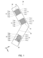
- FIG. 1 is a plan view showing an example of a module according to the present invention.
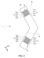
- FIG. 2 is a plan view showing an example of a module according to a reference example.
- FIG. 3 is a graph showing the relationship between the magnetization of the thin wire of the thermoelectric conversion portion and an external magnetic field.
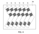
- FIG. 4 is a plan view showing an example of a method for manufacturing the module shown in FIG.
- FIG. 5 is a diagram showing an example of a sensor according to the present invention.
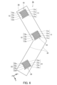
- FIG. 6 is a plan view showing another example of a module according to the present invention.
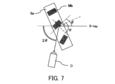
- FIG. 7 is a diagram showing a schematic diagram of a method for measuring the internal stress of a crystal.
- the module 1a includes a first heat flow detection unit 10 and a second heat flow detection unit 20.
- the first heat flow detection unit 10 and the second heat flow detection unit 20 are arranged on a substrate 30.
- the first heat flow detection unit 10 and the second heat flow detection unit 20 are arranged, for example, on a surface of the substrate 30 that forms the same plane.
- the first heat flow detection unit 10 includes a first thermoelectric conversion unit 11 and a first connection unit 12.
- the first thermoelectric conversion unit 11 forms a plurality of first thin wires 11a.
- the first connection unit 12 electrically connects the first thin wires 11a to each other.
- the first connection unit 12 forms a plurality of thin wires 12a.
- the multiple first thin wires 11a and the multiple second thin wires 21a extend parallel to each other. Therefore, for example, it is possible to carry out a process to impart predetermined thermoelectric conversion characteristics to these thin wires all at once, which tends to increase the productivity of the module 1a. In addition, there is little variation in the heat flow detection characteristics of the first heat flow detection unit 10 and the second heat flow detection unit 20. Therefore, according to the module 1a, it is easy to detect heat flows at multiple locations with high accuracy. For example, when the first heat flow detection unit 10 and the second heat flow detection unit 20 are arranged along the same plane, the multiple first thin wires 11a and the multiple second thin wires 21a extend parallel to each other.
- the multiple first thin wires 11a and the multiple second thin wires 21a extend, for example, along the Y-axis direction.
- the X-axis, Y-axis, and Z-axis are mutually perpendicular.
- the Z-axis is perpendicular to the surface of the substrate 30.
- the first thermoelectric conversion section 11 and the second thermoelectric conversion section 21 are arranged, for example, along a plane parallel to the XY plane.
- the second thin wires 21a extend non-parallel to the first thin wires 11a.
- the straight line extending the second thin wires 21a intersects with the straight line extending the first thin wires 11a.
- the first thermoelectric conversion unit 11 and the second thermoelectric conversion unit 21 are rotationally symmetric with respect to a rotation axis that passes through a specific point P1 on the XY plane and is parallel to the Z axis, for example.
- thermoelectric conversion characteristic to the thin wires included in the first thermoelectric conversion unit 11 and the second thermoelectric conversion unit 21. This is not advantageous from the viewpoint of the productivity of the module. Furthermore, if a process for imparting predetermined thermoelectric conversion characteristics to the fine wires contained in the first thermoelectric conversion unit 11 and the second thermoelectric conversion unit 21 is carried out at the same time, the variation in the heat flow detection characteristics in the first heat flow detection unit 10 and the second heat flow detection unit 20 is likely to increase, making it difficult to accurately detect heat flows at multiple locations.
- the second thermoelectric conversion section 21 includes, for example, second thin wires 21a having different lengths.
- the degree of freedom of the shape of the first thermoelectric conversion section 11 and the second thermoelectric conversion section 21 is likely to be high, and the shape of the first thermoelectric conversion section 11 and the second thermoelectric conversion section 21 is likely to be easily adjusted to match the shape of the substrate 30. For example, it is easy to reduce the dimension of the substrate 30 in a specific direction.
- the heat flow detection sensitivity of the first thermoelectric conversion section 11 and the second thermoelectric conversion section 21 can be proportional to, for example, the total length L1 of the multiple first thin wires 11a and the total length L2 of the multiple second thin wires 21a, respectively.
- the second thermoelectric conversion section 21 includes second thin wires 21a having different lengths, it is easy to align the area of the first thermoelectric conversion section 11 and the area of the second thermoelectric conversion section 21, and to align the width of the first thin wires 11a and the width of the second thin wires 21a, while aligning the heat flow detection sensitivity of the first heat flow detection section 10 and the second heat flow detection section 20.
- the coefficient of variation of the length of the second thin wires 21a in the second thermoelectric conversion section 21 is not limited to a specific value.
- the coefficient of variation is, for example, larger than the coefficient of variation of the length of the first thin wires 11a in the first thermoelectric conversion section 11.
- the coefficient of variation is, for example, 0.01 to 0.1, and may be 0.02 to 0.09, or may be 0.03 to 0.08.
- the coefficient of variation is a weighted coefficient of variation determined according to the following formulas (1) to (3).
- x i is the length of each thin wire.
- x wav is the weighted average of the lengths of the thin wires
- ⁇ is the standard deviation of the weighted average.
- w i is the weight of the length of each thin wire, and is the ratio of the length of each thin wire to the sum of the lengths of the thin wires.
- ⁇ i is the residual, which is the difference obtained by subtracting the weighted average x wav from the length of each thin wire, and n is the number of thin wires.
- Weighted coefficient of variation ⁇ / x wav Equation (1)
- the sensitivity of heat flow detection in the first heat flow detection unit 10 and the second heat flow detection unit 20 can be proportional to, for example, the sum L1 of the lengths of the multiple first thin wires 11a and the sum L2 of the lengths of the multiple second thin wires 21a, respectively. Therefore, in order to reduce the variation in the heat flow detection characteristics in the first heat flow detection unit 10 and the second heat flow detection unit 20, it is desirable that the difference between the sums L1 and L2 is small.
- the ratio L2/L1 of the sum L2 to the sum L1 is, for example, 0.90 to 1.10, preferably 0.95 to 1.05, and more preferably 0.99 to 1.01.
- the first thermoelectric conversion unit 11 generates an electromotive force in the length direction of the first thin wire 11a, for example, due to a heat flow perpendicular to the surface of the substrate 30 (Z-axis direction).
- the second thermoelectric conversion unit 21 generates an electromotive force in the length direction of the second thin wire 21a, for example, due to a heat flow perpendicular to the surface of the substrate 30.
- Each of the first thermoelectric conversion unit 11 and the second thermoelectric conversion unit 21 generates an electromotive force, for example, by the magneto-thermoelectric effect.
- the magneto-thermoelectric effect that generates the electromotive force in each of the first thermoelectric conversion unit 11 and the second thermoelectric conversion unit 21 may be the anomalous Nernst effect or the spin Seebeck effect. According to these magneto-thermoelectric effects, an electromotive force is generated in a direction perpendicular to the magnetization and perpendicular to the heat flow.
- the first thermoelectric conversion unit 11 and the second thermoelectric conversion unit 21 are, for example, perpendicular to the length direction (Y-axis direction) of the first thin wire 11a and the second thin wire 21a, respectively, and are magnetized in the width direction (X-axis direction) extending along the surface of the substrate 30.
- Each of the first thin wire 11a and the second thin wire 21a contains, for example, a predetermined magnetic material.
- the magnetic material contained in the first thin wire 11a has an easy magnetization axis, for example, perpendicular to the length direction of the first thin wire 11a and in the width direction (X-axis direction) extending along the surface of the substrate 30.
- the magnetic material contained in the second thin wire 21a has an easy magnetization axis, for example, perpendicular to the length direction of the second thin wire 21a and in the width direction (X-axis direction) extending along the surface of the substrate 30.
- the difference ⁇ 2 - ⁇ 1 obtained by subtracting the first internal stress ⁇ 1 of the first thin wire 11a from the second internal stress ⁇ 2 of the first thin wire 11a is not limited to a specific value.
- the difference ⁇ 2 - ⁇ 1 is, for example, 50 MPa or more.
- the difference ⁇ 2 - ⁇ 1 obtained by subtracting the first internal stress ⁇ 1 of the second thin wire 21a from the second internal stress ⁇ 2 of the second thin wire 21a is not limited to a specific value.
- the difference ⁇ 2 - ⁇ 1 is, for example, 50 MPa or more.
- the first internal stress ⁇ 1 is the internal stress of the first thin wire 11a or the second thin wire 21a in a first direction parallel to the surface of the substrate 30.
- the second internal stress ⁇ 2 is the internal stress of the first thin wire 11a or the second thin wire 21a in a second direction parallel to the surface of the substrate 30 and perpendicular to the first direction.
- the first fine wire 11a or the second fine wire 21a is likely to have an easy magnetization axis in the width direction of the first fine wire 11a or the width direction of the second fine wire 21a, respectively.
- thermoelectric conversion unit 11 and the second thermoelectric conversion unit 21 This makes it easy for the first thermoelectric conversion unit 11 and the second thermoelectric conversion unit 21 to exhibit desired thermoelectric performance, and the sensitivity of heat flow detection in the first heat flow detection unit 10 and the second heat flow detection unit 20 is likely to be high.
- a positive internal stress indicates a tensile stress
- a negative internal stress indicates a compressive stress.
- FIG. 3 is a graph showing an example of the relationship between the magnetization of the first thin wire 11a and the second thin wire 21a and the external magnetic field.
- the solid line graph shows the relationship between the magnetization of the first thin wire 11a and the second thin wire 21a in the second direction and the external magnetic field.
- the dashed line graph shows the relationship between the magnetization of the first thin wire 11a and the second thin wire 21a in the first direction and the external magnetic field.
- the difference ⁇ 2 - ⁇ 1 is 50 MPa or more, so that the magnetic properties of the first fine wire 11a and the second fine wire 21a have large anisotropy in the second direction and the first direction. Due to such large anisotropy of the magnetic properties, the first fine wire 11a and the second fine wire 21a are likely to have an easy magnetization axis in the second direction and a hard magnetization axis in the first direction. As a result, each of the first fine wire 11a and the second fine wire 21a is likely to exhibit stable behavior against an external magnetic field, and each of the first thermoelectric conversion unit 11 and the second thermoelectric conversion unit 21 is likely to exhibit the desired thermoelectric performance.
- the difference ⁇ 2 - ⁇ 1 may be 100 MPa or more, 150 MPa or more, or 200 MPa or more.
- the upper limit of the difference ⁇ 2 - ⁇ 1 is not limited to a specific value.
- the difference ⁇ 2 - ⁇ 1 is, for example, 900 MPa or less. In this case, even if a bending load in the second direction is applied to both ends of the first thin wire 11a and the second thin wire 21a, cracks are unlikely to occur in the first thin wire 11a and the second thin wire 21a.
- the first internal stress ⁇ 1 may be a tensile stress or a compressive stress.
- the first internal stress ⁇ 1 is, for example, 900 MPa or less. This makes it easy to adjust the difference ⁇ 2 - ⁇ 1 in the first thin wire 11a and the second thin wire 21a to 50 MPa or more. In addition, even if a bending load in the first direction is applied to both ends of the first thin wire 11a and the second thin wire 21a, cracks are unlikely to occur in the first thin wire 11a and the second thin wire 21a.
- the first internal stress ⁇ 1 is, for example, -900 MPa or more.
- the first internal stress ⁇ 1 may be included in any of the ranges determined by all combinations of a lower limit value that is any one of -900 MPa, -700 MPa, -500 MPa, and -300 MPa and an upper limit value that is any one of 900 MPa, 700 MPa, 500 MPa, and 300 MPa.
- the second internal stress ⁇ 2 may be a tensile stress or a compressive stress.
- the second internal stress ⁇ 2 is, for example, -900 MPa or more. This makes it easy to adjust the difference ⁇ 2 - ⁇ 1 to 50 MPa or more.
- the second internal stress ⁇ 2 is, for example, 900 MPa or less. In this case, even if a bending load in the second direction is applied to both ends of the first fine wire 11a and the second fine wire 21a, cracks are unlikely to occur in the first fine wire 11a and the second fine wire 21a.
- the second internal stress ⁇ 2 may be included in any of the ranges determined by all combinations of a lower limit value that is any one of -900 MPa, -700 MPa, -500 MPa, and -300 MPa and an upper limit value that is any one of 900 MPa, 700 MPa, 500 MPa, and 300 MPa.
- the magnetostriction constant of the magnetic material contained in the first thin wire 11a and the second thin wire 21a may be a positive value or a negative value.
- the magnetostriction constant of the magnetic material is a positive value
- the Y-axis direction corresponds to the first direction
- the X-axis direction corresponds to the second direction.
- the magnetostriction constant of the magnetic material contained in the first thin wire 11a and the second thin wire 21a is a negative value
- the X-axis direction corresponds to the first direction
- the Y-axis direction corresponds to the second direction.
- the first thin wire 11a and the second thin wire 21a extend in the Y-axis direction, so that in the first thin wire 11a and the second thin wire 21a, when considering the shape magnetic anisotropy, it seems that the magnetization easy axis occurs in the Y-axis direction and the magnetization hard axis occurs in the X-axis direction.
- the difference ⁇ 2 - ⁇ 1 in the first thin wire 11a and the second thin wire 21a is 50 MPa or more, the magnetic properties of the first thin wire 11a and the second thin wire 21a have large anisotropy in the second direction and the first direction as described above.
- the first thin wire 11a and the second thin wire 21a are likely to have an easy magnetization axis in the X-axis direction, and each of the first thin wire 11a and the second thin wire 21a is likely to exhibit stable behavior against an external magnetic field, and as a result, each of the first thermoelectric conversion section 11 and the second thermoelectric conversion section 21 is likely to exhibit desired thermoelectric performance.
- the first thin wire 11a and the second thin wire 21a contain, for example, a material exhibiting the anomalous Nernst effect.
- the material exhibiting the anomalous Nernst effect is not limited to a specific material.
- the material exhibiting the anomalous Nernst effect is, for example, a magnetic material having a saturation magnetic susceptibility of 5 ⁇ 10 ⁇ 3 T or more or a material having a band structure with a Weyl point in the vicinity of the Fermi energy.
- the magnetic material may be a ferrimagnetic material.
- the first thin wire 11a and the second thin wire 21a contain, for example, at least one material selected from the group consisting of the following (i), (ii), (iii), (iv), and (v) as the material exhibiting the anomalous Nernst effect.
- X is a typical element or a transition element.
- X is, for example, Al, Ga, Ge, Sn, Si, Ti, Zr, Hf, V, Nb, Ta, Cr, Mo, W, Sc, Ni, Mn, or Co.
- the combination of M1 and M2 is not limited to a specific combination as long as M1 and M2 are different typical elements.
- the combination of M1 and M2 is, for example, Ga and Al, Si and Al, or Ga and B.
- the magnetic thin film 11 may contain Co 2 MnGa or Mn 3 Sn as a material exhibiting the anomalous Nernst effect.
- the absolute value of the magnetostriction constant ⁇ may be 10 ⁇ 10 ⁇ 6 or more, or may be 20 ⁇ 10 ⁇ 6 or more.
- the multiple first thin wires 11a are electrically connected in series by the first connection unit 12.
- the multiple second thin wires 21a are electrically connected in series by the second connection unit 22.
- the first heat flow detection unit 10 has, for example, a meander pattern.
- the second heat flow detection unit 20 has a meander pattern.
- the thickness of the first thin wire 11a and the second thin wire 21a may be included in any of the ranges determined by all combinations of a lower limit value of any one of 5 nm, 10 nm, 20 nm, 30 nm, and 50 nm and an upper limit value of any one of 1000 nm, 750 nm, 500 nm, 400 nm, 300 nm, and 200 nm.
- the width which is the dimension in the X-axis direction of the first thin wire 11a and the second thin wire 21a, is not limited to a specific value. This width is, for example, 500 ⁇ m or less. This allows the amount of material used to form the magnetic thermoelectric converter in the thermoelectric conversion element 100 to be reduced, making it easy to reduce the manufacturing cost of the thermoelectric conversion element 100. In addition, it is easy to arrange a large number of first thin wires 11a and second thin wires 21a in the X-axis direction, making it easy to increase the sensitivity of heat flow detection in the first heat flow detection unit 10 and the second heat flow detection unit 20. The width of the first thin wire 11a and the second thin wire 21a is, for example, 0.1 ⁇ m or more. Breaks are less likely to occur in the first heat flow detection unit 10 and the second heat flow detection unit 20, making it easy for the module 1a to exhibit high durability.
- the width of the first thin wire 11a and the second thin wire 21a may be included in any of the ranges determined by all combinations of a lower limit value of any one of 0.1 ⁇ m, 0.5 ⁇ m, 1 ⁇ m, 2 ⁇ m, 5 ⁇ m, 10 ⁇ m, 20 ⁇ m, and 30 ⁇ m and an upper limit value of any one of 500 ⁇ m, 400 ⁇ m, 300 ⁇ m, 200 ⁇ m, 100 ⁇ m, and 50 ⁇ m.
- the thickness which is the dimension in the Z-axis direction of the thin wires 12a and 22a, is not limited to a specific value.
- the thickness is, for example, 1000 nm or less. This allows the amount of material used to form the first connection portion 12 and the second connection portion 22 to be reduced, making it easier to reduce the manufacturing costs of the module 1a. In addition, breaks are less likely to occur in the first heat flow detection portion 10 and the second heat flow detection portion 20.
- the thickness of the thin wires 12a and 22a is, for example, 5 nm or more. This makes it easier for the module 1a to exhibit high durability.
- the width of the thin wires 12a and 22a is not limited to a specific value. This width is, for example, 500 ⁇ m or less. This allows the amount of material used to form the first connection portion 12 and the second connection portion 22 to be reduced, making it easier to reduce the manufacturing costs of the module 1a. In addition, it is easy to arrange a large number of thin wires 12a and 22a, making it easier to increase the sensitivity of heat flow detection in the first heat flow detection portion 10 and the second heat flow detection portion 20.
- the width of the thin wires 12a and 22a is, for example, 0.1 ⁇ m or more. This makes it harder for breaks to occur in the first heat flow detection portion 10 and the second heat flow detection portion 20, making it easier for the module 1a to exhibit high durability.
- the width of the thin wire 12a and the thin wire 22a may be included in any of the ranges determined by all combinations of a lower limit value of 0.1 ⁇ m, 0.5 ⁇ m, 1 ⁇ m, 2 ⁇ m, 5 ⁇ m, 10 ⁇ m, 20 ⁇ m, and 30 ⁇ m and an upper limit value of 500 ⁇ m, 400 ⁇ m, 300 ⁇ m, 200 ⁇ m, 100 ⁇ m, and 50 ⁇ m.
- the substrate 30 is not limited to a specific substrate as long as it can provide a surface on which the first heat flow detection unit 10 and the second heat flow detection unit 20 are disposed.
- the surface of the substrate 30 on which the first heat flow detection unit 10 and the second heat flow detection unit 20 are disposed is formed, for example, from a dielectric material.
- the material forming the substrate 30 may be an organic polymer or an inorganic material such as glass or ceramics. Examples of organic polymers are polyethylene terephthalate (PET), polyethylene naphthalate (PEN), acrylic resin (PMMA), polycarbonate (PC), polyimide (PI), or cycloolefin polymer (COP).
- the substrate 30 has, for example, flexibility.
- the substrate 30 has elasticity that allows the test specimen to be elastically deformed when, for example, a strip-shaped test specimen made from the substrate 20 is wound around a cylindrical mandrel having a diameter of 10 cm so that both ends in the longitudinal direction of the test specimen face in the same direction.
- the substrate may be rigid.
- the substrate 30 may be, for example, in the form of a sheet, a film, or a plate.
- the thickness of the substrate 30 is not limited to a specific thickness.
- the thickness of the substrate 30 is, for example, 4 to 250 ⁇ m.
- thermoelectric conversion section 11 and the second thermoelectric conversion section 21 are formed on one main surface of a large or long substrate 30a by a method such as sputtering, chemical vapor deposition (CVD), pulsed laser deposition (PLD), ion plating, and plating.
- CVD chemical vapor deposition
- PLD pulsed laser deposition
- ion plating ion plating
- plating plating
- the substrate 30a and the film of the precursor of the first thermoelectric conversion section 11 and the second thermoelectric conversion section 21 are heated at a predetermined temperature as necessary.
- the temperature of the heat treatment is not limited to a specific temperature.
- the ambient temperature of the substrate 30a and the precursor of the first thermoelectric conversion section 11 and the second thermoelectric conversion section 21 in the heat treatment is, for example, 50° C.
- the ambient temperature of the substrate 30a and the precursor of the first thermoelectric conversion section 11 and the second thermoelectric conversion section 21 in the heat treatment may be 100° C. or higher, 150° C. or higher, or 200° C. or higher, for example, 300° C. or lower.
- the time during which the ambient temperature of the substrate 30a is maintained at 50°C or higher during the heat treatment is not limited to a specific value.
- the time is, for example, 10 minutes or more and 3 hours or less.
- a photoresist is applied onto the film of the precursor of the first thermoelectric conversion unit 11 and the second thermoelectric conversion unit 21, a photomask is placed on the film and exposed to light, and then wet etching is performed. As a result, a plurality of fine lines arranged at a predetermined interval are formed.
- a film of the precursor of the first connection unit 12 and the second connection unit 22 is formed on one main surface of the base material 30a by a method such as sputtering, CVD, PLD, ion plating, and plating.
- a photoresist is applied onto this film, a photomask is placed on the film and exposed to light, and then wet etching is performed.
- the first connection unit 12 and the second connection unit 22 are formed, and the fine lines of the precursor of the first thermoelectric conversion unit 11 and the second thermoelectric conversion unit 21 are electrically connected to each other.
- a plurality of semi-finished products 2a of modules 1a are produced on one base material 30a.
- each semi-finished product 2a is cut out from the substrate 30a, and the thin wires of the precursors of the first thermoelectric conversion section 11 and the second thermoelectric conversion section 21 in each semi-finished product 2a are magnetized to obtain the first thermoelectric conversion section 11 and the second thermoelectric conversion section 21. In this manner, the module 1a is obtained.
- Module 1a may be provided, for example, together with an adhesive layer.
- the base material 30 in the thickness direction of the base material 30, the base material 30 is disposed between the first thermoelectric conversion unit 11 and the second thermoelectric conversion unit 21 and the adhesive layer. This allows the adhesive layer to be pressed against an article to attach module 1a to the article.
- the adhesive layer contains, for example, a rubber-based adhesive, an acrylic-based adhesive, a silicone-based adhesive, or a urethane-based adhesive.
- Module 1a may be provided together with the adhesive layer and a release liner.
- the release liner covers the adhesive layer.
- the release liner is typically a film that can maintain the adhesive force of the adhesive layer when covering the adhesive layer, and can be easily peeled off from the adhesive layer.
- the release liner is, for example, a film made of a polyester resin such as PET. The adhesive layer is exposed by peeling off the release liner, and module 1a can be attached to an article.
- a sensor 5 including a module 1a can be provided.
- this sensor 5 when a temperature gradient occurs in the thickness direction of the substrate 30, for example, an electromotive force is generated in the length direction (Y-axis direction) of the first thin wire 11a and the second thin wire 12a in the first thermoelectric conversion unit 11 and the second thermoelectric conversion unit 21, respectively.
- the sensor 5 can detect, for example, the heat flux [W/ m2 ] at the locations corresponding to the first thermoelectric conversion unit 11 and the second thermoelectric conversion unit 21 by processing an electric signal based on this electromotive force outputted to the outside of the module 1a.
- the senor 5 further includes, for example, a signal processing device 2.
- the signal processing device 2 processes the electrical signal outputted to the outside of the module 1a.
- Module 1a can be modified in various respects.
- module 1a may be modified to module 1b shown in FIG. 6.
- Module 1b is configured in the same manner as module 1a, except for the parts that are specifically described. The description of module 1a also applies to module 1b, so long as there is no technical contradiction.
- the lengths of the multiple second thin wires 21a in the second thermoelectric conversion section 21 are approximately the same.
- the coefficient of variation of the length of the second thin wires 21a in the second thermoelectric conversion section 21 is not limited to a specific value.
- the coefficient of variation is, for example, approximately the same as the coefficient of variation of the length of the first thin wires 11a in the first thermoelectric conversion section 11.
- the conductive paths a, b, and c were formed as follows.
- the temperature of the PET film was adjusted to 100 ° C.
- the PET film on which the magnetic thin film was formed was heated for 30 minutes in an environment of 150 ° C. Next, a photoresist was applied on the magnetic thin film, a photomask was placed on the magnetic thin film, exposure was performed, and then wet etching was performed. As a result, 62 FeGa-containing thin lines arranged at a predetermined interval were formed.
- each FeGa-containing linear pattern was 100 ⁇ m.
- a Cu thin film having a thickness of 100 nm was formed by DC magnetron sputtering using a target material containing Cu.
- a photoresist was applied on the Cu thin film, a photomask was placed on the Cu thin film, exposure was performed, and then wet etching was performed.
- a Cu-containing thin line having a width of 40 ⁇ m was formed.
- a pair of adjacent FeGa-containing fine wires was electrically connected to each other by the Cu-containing fine wires, forming conductive paths a, b, and c that formed a meander pattern.
- the length of each of the 62 FeGa-containing thin wires was approximately the same, 7 mm.
- the 62 FeGa-containing thin wires included FeGa-containing thin wires of different lengths.
- the 186 FeGa-containing thin wires were parallel to each other and extended in a direction perpendicular to one of the two line segments forming an angle of 150°.
- each of the conductive paths a, b, and c the sum of the lengths of the 62 FeGa-containing thin wires was the same.
- the conductive paths a, b, and c were rectangular in plan view, and the short side of the outer shape of each conductive path extended in the width direction of the PET film.
- the FeGa-containing thin wire was magnetized in the width direction parallel to the main surface of the PET film and perpendicular to the length direction of the FeGa-containing thin wire. In this way, the module according to Example 1 was obtained.
- Example 2 A module according to Example 2 was obtained in the same manner as in Example 1, except for the following points.
- the length of each of the 62 FeGa-containing thin wires was adjusted to be approximately equal, 7 mm, as shown in Fig. 6.
- the conductive paths a, b, and c were formed so as to overlap each other by moving parallel to the main surface of the PET film.
- the width of the PET film was 20.5 mm.
- Comparative Example 1 A module according to Comparative Example 1 was obtained in the same manner as in Example 1, except for the following points. Instead of the conductive paths a, b, and c, conductive paths ⁇ and ⁇ were formed. The conductive paths ⁇ and ⁇ were disposed at the ends of the PET film. The conductive path ⁇ was formed in the same manner as the conductive path a. The conductive path ⁇ was formed in the same manner as the conductive path c, except for the parts that will be particularly described. The FeGa-containing thin wire in the conductive path ⁇ was non-parallel to the FeGa-containing thin wire in the conductive path ⁇ . As shown in FIG.
- the FeGa-containing thin wire in the conductive path ⁇ extended in a direction perpendicular to one of the two line segments that form an angle of 150°
- the FeGa-containing thin wire in the conductive path ⁇ extended in a direction perpendicular to the other of the two line segments.
- the conductive paths ⁇ and ⁇ were rectangular in plan view, and the short sides of the outline of each conductive path extended in the width direction of the PET film.
- the conductive paths ⁇ and ⁇ were configured to be rotationally symmetric.
- the width of the PET film was 10 mm.
- Magnetic properties The magnetic properties of the FeGa-containing thin wire of the module according to each example and each comparative example were measured using a small cryogen-free physical property measurement system PPMS-versalab from Qantum Design. For this measurement, a measurement sample was used, which was prepared by cutting out the part of the module according to each example and each comparative example where each conductive path was arranged into a 2 mm square.
- a vibration sample magnetrometer VSM was used to sweep a magnetic field of ⁇ 800 [kA/m] in a direction parallel to the magnetization direction of the magnetized FeGa-containing thin wire, and an M-H curve was obtained under the condition of a temperature of 300 K, taking into account the thickness of the FeGa-containing thin wire and the area of the FeGa-containing thin wire in the measurement sample.
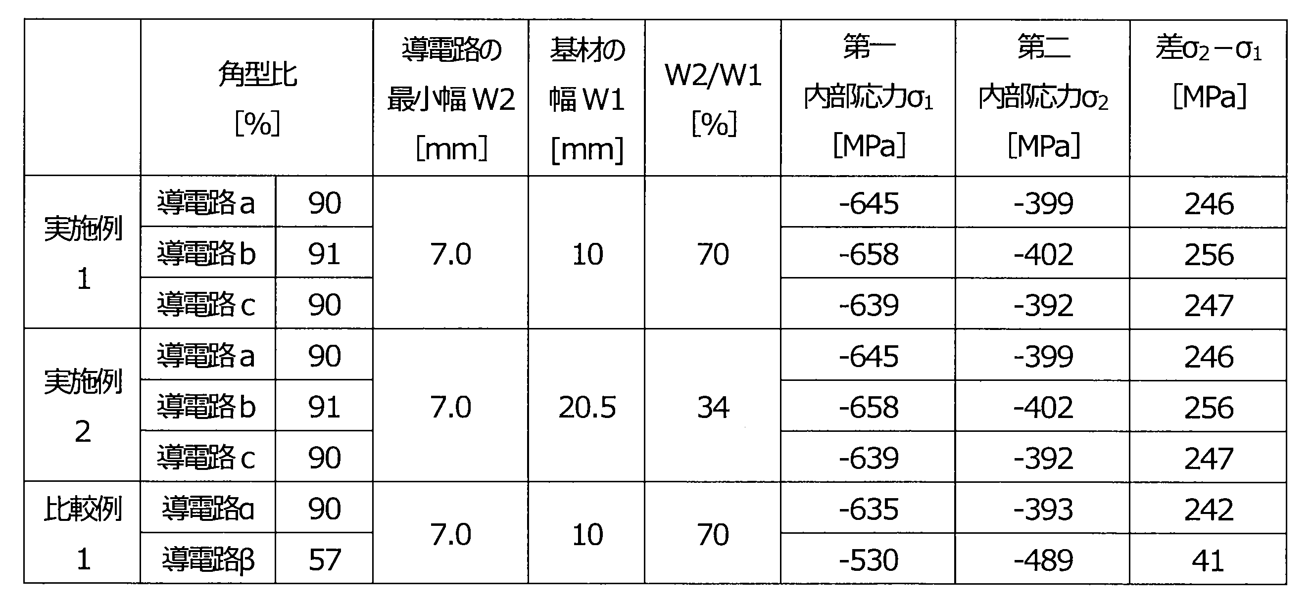
- the ratio Mr/Ms of the magnetization Ms value of ⁇ 800 [kA/m] to the magnetization Mr value of 0 [kA/m] during the magnetic field sweep was determined as the squareness ratio. The results are shown in Table 1.
- the wavelength ⁇ of the Cu-K ⁇ rays was 0.1541 nm.
- the sin 2 ⁇ method is a method for determining the internal stress of a thin film from the dependence of the crystal lattice distortion of the polycrystalline thin film on the angle ( ⁇ ).
- the integration time at each measurement point was set to 100 seconds.
- the crystal lattice spacing d of the magnetic material at each measurement angle ( ⁇ ) was calculated from the peak angle 2 ⁇ of the obtained X-ray diffraction and the wavelength ⁇ of the X-ray irradiated from the light source, and the crystal lattice distortion ⁇ was calculated from the crystal lattice spacing d according to the relationship of the following formulas (4) and (5).
- the above-mentioned X-ray diffraction measurement was performed in each case where the angle ( ⁇ ) between the normal to the main surface of the sample Sa and the normal to the crystal plane of the crystal Mb was 0°, 17°, 24°, 30°, 35°, 40°, and 45°, and the crystal lattice strain ⁇ at each angle ( ⁇ ) was calculated. Then, the first internal stress ⁇ 1 and the second internal stress ⁇ 2 were calculated from the slope of the line plotting the relationship between sin 2 ⁇ and the crystal lattice strain ⁇ using the following formula (6). The results are shown in Table 1. In the internal stress in Table 1, positive values indicate tensile stress and negative values indicate compressive stress.
- E is the Young's modulus of the magnetic material (130 GPa)
- ⁇ is the Poisson's ratio of the magnetic material (0.3).
- Detector D in Figure 7 detects X-ray diffraction.
- Example 2 A comparison between Examples 1 and 2 suggested that the conductive path c in Example 2 had a larger dimension in the width direction of the substrate, and therefore that the width of the PET film also needed to be increased. This suggests that if the lengths of the FeGa-containing thin wires in the conductive path c are different, as in Example 1, it is easier to miniaturize the module.
- the first aspect of the present invention is a first heat flow detection unit disposed on a substrate, the first heat flow detection unit including a first thermoelectric conversion unit including a plurality of first thin wires and a first connection unit electrically connecting the first thin wires to each other; a second heat flow detection unit disposed on the base material and including a second thermoelectric conversion unit forming a plurality of second thin wires and a second connection unit electrically connecting the second thin wires to each other; The first thin wires and the second thin wires extend parallel to each other. Provide a module.
- thermoelectric conversion unit includes the second thin wires having different lengths.
- a module according to a first aspect is provided.
- a third aspect of the present invention is The substrate has a pair of edge lines that overlap each other by translation in a plan view.
- a module according to the first or second aspect is provided.
- a fourth aspect of the present invention is the first thermoelectric conversion unit generates an electromotive force in a longitudinal direction of the first thin wire by a heat flow in a direction perpendicular to a surface of the base material, the second thermoelectric conversion unit generates an electromotive force in a longitudinal direction of the second thin wire by a heat flow in a direction perpendicular to the surface of the base material;
- a module according to any one of the first to third aspects is provided.
- a fifth aspect of the present invention is the first fine wire includes a magnetic body having an easy axis of magnetization in a width direction perpendicular to a length direction of the first fine wire and extending along a surface of the base material;
- the second fine wire includes a magnetic body having an easy axis of magnetization in a width direction perpendicular to a longitudinal direction of the second fine wire and extending along a surface of the base material;
- a sixth aspect of the present invention is a difference obtained by subtracting the first internal stress of the first thin wire from the second internal stress of the first thin wire is 50 MPa or more; A difference between the second internal stress of the second thin wire and the first internal stress of the second thin wire is 50 MPa or more; the first internal stress is an internal stress of the first thin wire or the second thin wire in a first direction parallel to a surface of the base material; The second internal stress is an internal stress of the first thin wire or the second thin wire in a second direction parallel to a surface of the base material and perpendicular to the first direction.
- a module according to any one of the first to fifth aspects is provided.
- a seventh aspect of the present invention is The first heat flow detection portion has a meander pattern, The second heat flow detection portion has a meander pattern.
- a module according to any one of the first to sixth aspects is provided.
- An eighth aspect of the present invention is A module according to any one of the first to seventh aspects is provided.
- a heat flow sensor is provided.
Landscapes
- Physics & Mathematics (AREA)
- General Physics & Mathematics (AREA)
- Chemical & Material Sciences (AREA)
- Engineering & Computer Science (AREA)
- Combustion & Propulsion (AREA)
- Measuring Temperature Or Quantity Of Heat (AREA)
Abstract
Description
基材上に配置され、複数の第一細線をなす第一熱電変換部と、前記第一細線同士を電気的に接続する第一接続部とを含む第一熱流検知部と、
前記基材上に配置され、複数の第二細線をなす第二熱電変換部と、前記第二細線同士を電気的に接続する第二接続部とを含む第二熱流検知部と、を備え、
前記複数の第一細線及び前記複数の第二細線は、互いに平行に延びている、
モジュールを提供する。
上記モジュールを備えた、
熱流センサを提供する。
重み付き変動係数=σ/xwav 式(1)


(i)Fe3Xで表される組成を有するストイキオメトリックな物質
(ii)上記(i)の物質からFeとXとの組成比がずれたオフ・ストイキオメトリックな物質
(iii)上記(i)の物質のFeサイトの一部又は上記(ii)の物質のFeサイトの一部がX以外の典型金属元素又は遷移元素で置換された物質
(iv)Fe3M11-xM2x(0<x<1)で表される組成を有し、M1及びM2が互いに異なる典型元素である物質
(v)上記(i)の物質のFeサイトの一部がX以外の遷移元素で置換され、上記(i)の物質のXサイトの一部がX以外の典型金属元素で置換された物質
平面視で図1に示すようなV字状の形状を有し、かつ、50μmの厚さを有するポリエチレンテレフタレート(PET)フィルム上に、メアンダパターンをなす3つの導電路a、b、及びcを形成した。PETフィルムは、150°の角度をなす2つの線分に沿って帯状に延びていた。PETフィルムの平面視において、導電路a及び導電路cはPETフィルムの端部に配置されており、導電路bは、PETフィルムの中央部に配置されていた。導電路a及びbは、150°の角度をなす2つの線分の一方に沿って配置されていた。PETフィルムの幅は10mmであった。
下記の点以外は、実施例1と同様にして、実施例2に係るモジュールを得た。導電路cにおいて、62本の各FeGa含有細線の長さは、図6に示すように概ね等しく、7mmになるように調整した。導電路a、b、及びcは、PETフィルムの主面に沿って平行移動することにより互いに重なり合うように形成されていた。PETフィルムの幅は20.5mmであった。
下記の点以外は、実施例1と同様にして、比較例1に係るモジュールを得た。導電路a、b、及びcに代えて、導電路α及びβを形成した。導電路α及び導電路βはPETフィルムの端部に配置されていた。導電路αは、導電路aと同様に形成した。導電路βは、特に説明する部分を除き、導電路cと同様に形成した。導電路βにおけるFeGa含有細線は、導電路αにおけるFeGa含有細線と非平行であった。導電路αにおけるFeGa含有細線は、図2に示すように、上記の150°の角度をなす2つの線分の一方と垂直な方向に延びており、導電路βにおけるFeGa含有細線は、その2つの線分の他方と垂直な方向に延びていた。導電路α及びβは平面視において長方形状であり、各導電路の外形の短辺がPETフィルムの幅方向に延びていた。導電路α及び導電路βは回転対称に構成されていた。PETフィルムの幅は10mmであった。
Qantum Design社の小型無冷媒型物理特性測定システム PPMS-versalabを用いて、各実施例及び各比較例に係るモジュールのFeGa含有細線の磁気物性を測定した。この測定には、各実施例及び各比較例に係るモジュールの各導電路が配置された部分を2mm平方に切り取って作製した測定サンプルを用いた。加えて、測定では、Vibration Sample Magnetrometer(VSM)を使用し、磁化されたFeGa含有細線の磁化方向に平行方向に±800[kA/m]の磁場を掃引し、温度300Kの条件で、FeGa含有細線の厚さ及び測定サンプルにおけるFeGa含有細線の面積を考慮して、M‐H曲線を得た。±800[kA/m]の磁化Msの値と磁場掃引時の0[kA/m]の磁化Mrの値の比Mr/Msを角型比と決定した。結果を表1に示す。
リガク社製のX線回折装置 Smartlabを用いて、40kV及び50mAの光源からCu‐Kα線を、平行ビーム光学系を通過させて試料に照射し、sin2Ψ法の測傾法の原理で各実施例及び各比較例におけるFeGa含有細線の第一内部応力σ1及び第二内部応力σ2を測定した。第一内部応力σ1は、FeGa含有細線の長さ方向における内部応力であり、第二内部応力σ2は、PETフィルムの主面に平行であり、かつ、FeGa含有細線の長さ方向に垂直な幅方向における内部応力であった。Cu‐Kα線の波長λは、0.1541nmであった。sin2Ψ法は、多結晶薄膜の結晶格子歪みの角度(Ψ)に対する依存性から、薄膜の内部応力を求める手法である。上記のX線回折装置を用い、θ/2θスキャン測定によって、2θ=75°~85°の範囲において0.01°おきに回折強度を測定した。各測定点における積算時間は100秒に設定した。得られたX線回折のピーク角2θと、光源から照射されたX線の波長λとから、各測定角度(Ψ)における磁性体の結晶格子面間隔dを算出し、結晶格子面間隔dから下記の式(4)及び式(5)の関係から結晶格子歪みεを算出した。λは、光源から照射されたX線(Cu‐Kα線)の波長であり、λ=0.1541nmである。d0は、無応力状態の結晶の格子面間隔であり、d0=0.0206nmである。
2dsinθ=λ 式(4)
ε=(d-d0)/d0 式(5)
ε={(1+ν)/E}σsin2Ψ-(2ν/E)σ 式(6)
基材上に配置され、複数の第一細線をなす第一熱電変換部と、前記第一細線同士を電気的に接続する第一接続部とを含む第一熱流検知部と、
前記基材上に配置され、複数の第二細線をなす第二熱電変換部と、前記第二細線同士を電気的に接続する第二接続部とを含む第二熱流検知部と、を備え、
前記複数の第一細線及び前記複数の第二細線は、互いに平行に延びている、
モジュールを提供する。
前記第二熱電変換部は、異なる長さを有する前記第二細線を含む、
第1側面に係るモジュールを提供する。
前記基材は、平面視において平行移動により重なり合う一対の端線を有する、
第1側面又は第2側面に係るモジュールを提供する。
前記第一熱電変換部は、前記基材の表面に垂直な方向の熱流により前記第一細線の長さ方向に起電力を生じさせ、
前記第二熱電変換部は、前記基材の表面に垂直な方向の熱流により前記第二細線の長さ方向に起電力を生じさせる、
第1側面~第3側面のいずれか1つに係るモジュールを提供する。
前記第一細線は、前記第一細線の長さ方向に垂直であり、かつ、前記基材の表面に沿って延びる幅方向に磁化容易軸を有する磁性体を含み、
前記第二細線は、前記第二細線の長さ方向に垂直であり、かつ、前記基材の表面に沿って延びる幅方向に磁化容易軸を有する磁性体を含む、
第1側面~第4側面のいずれか1つに係るモジュールを提供する。
前記第一細線の第二内部応力から前記第一細線の第一内部応力を差し引いた差は、50MPa以上であり、
前記第二細線の第二内部応力から前記第二細線の第一内部応力を差し引いた差は、50MPa以上であり、
前記第一内部応力は、前記基材の表面に平行な第一方向における前記第一細線又は前記第二細線の内部応力であり、
前記第二内部応力は、前記基材の表面に平行であり、かつ、前記第一方向に垂直な第二方向における前記第一細線又は前記第二細線の内部応力である、
第1側面~第5側面のいずれか1つに係るモジュールを提供する。
前記第一熱流検知部は、メアンダパターンをなしており、
前記第二熱流検知部は、メアンダパターンをなしている、
第1側面~第6側面のいずれか1つに係るモジュールを提供する。
第1側面~第7側面のいずれか1つに係るモジュールを備えた、
熱流センサを提供する。
Claims (8)
- 基材上に配置され、複数の第一細線をなす第一熱電変換部と、前記第一細線同士を電気的に接続する第一接続部とを含む第一熱流検知部と、
前記基材上に配置され、複数の第二細線をなす第二熱電変換部と、前記第二細線同士を電気的に接続する第二接続部とを含む第二熱流検知部と、を備え、
前記複数の第一細線及び前記複数の第二細線は、互いに平行に延びている、
モジュール。 - 前記第二熱電変換部は、異なる長さを有する前記第二細線を含む、
請求項1に記載のモジュール。 - 前記基材は、平面視において平行移動により重なり合う一対の端線を有する、
請求項1に記載のモジュール。 - 前記第一熱電変換部は、前記基材の表面に垂直な方向の熱流により前記第一細線の長さ方向に起電力を生じさせ、
前記第二熱電変換部は、前記基材の表面に垂直な方向の熱流により前記第二細線の長さ方向に起電力を生じさせる、
請求項1に記載のモジュール。 - 前記第一細線は、前記第一細線の長さ方向に垂直であり、かつ、前記基材の表面に沿って延びる幅方向に磁化容易軸を有する磁性体を含み、
前記第二細線は、前記第二細線の長さ方向に垂直であり、かつ、前記基材の表面に沿って延びる幅方向に磁化容易軸を有する磁性体を含む、
請求項1に記載のモジュール。 - 前記第一細線の第二内部応力から前記第一細線の第一内部応力を差し引いた差は、50MPa以上であり、
前記第二細線の第二内部応力から前記第二細線の第一内部応力を差し引いた差は、50MPa以上であり、
前記第一内部応力は、前記基材の表面に平行な第一方向における前記第一細線又は前記第二細線の内部応力であり、
前記第二内部応力は、前記基材の表面に平行であり、かつ、前記第一方向に垂直な第二方向における前記第一細線又は前記第二細線の内部応力である、
請求項1に記載のモジュール。 - 前記第一熱流検知部は、メアンダパターンをなしており、
前記第二熱流検知部は、メアンダパターンをなしている、
請求項1に記載のモジュール。 - 請求項1から7のいずれか1項に記載のモジュールを備えた、
熱流センサ。
Priority Applications (2)
| Application Number | Priority Date | Filing Date | Title |
|---|---|---|---|
| CN202480014394.8A CN120827019A (zh) | 2023-03-31 | 2024-03-07 | 模组及热流传感器 |
| JP2025510182A JPWO2024203137A1 (ja) | 2023-03-31 | 2024-03-07 |
Applications Claiming Priority (2)
| Application Number | Priority Date | Filing Date | Title |
|---|---|---|---|
| JP2023057429 | 2023-03-31 | ||
| JP2023-057429 | 2023-03-31 |
Publications (1)
| Publication Number | Publication Date |
|---|---|
| WO2024203137A1 true WO2024203137A1 (ja) | 2024-10-03 |
Family
ID=92904476
Family Applications (1)
| Application Number | Title | Priority Date | Filing Date |
|---|---|---|---|
| PCT/JP2024/008893 Ceased WO2024203137A1 (ja) | 2023-03-31 | 2024-03-07 | モジュール及び熱流センサ |
Country Status (3)
| Country | Link |
|---|---|
| JP (1) | JPWO2024203137A1 (ja) |
| CN (1) | CN120827019A (ja) |
| WO (1) | WO2024203137A1 (ja) |
Citations (3)
| Publication number | Priority date | Publication date | Assignee | Title |
|---|---|---|---|---|
| WO2013153949A1 (ja) * | 2012-04-11 | 2013-10-17 | 日本電気株式会社 | 磁界測定装置及び磁界測定方法 |
| JP2018004475A (ja) * | 2016-07-04 | 2018-01-11 | 株式会社デンソー | 熱流束センサモジュールおよびその製造方法 |
| WO2022176966A1 (ja) * | 2021-02-17 | 2022-08-25 | 国立大学法人東京大学 | 熱電装置 |
-
2024
- 2024-03-07 CN CN202480014394.8A patent/CN120827019A/zh active Pending
- 2024-03-07 WO PCT/JP2024/008893 patent/WO2024203137A1/ja not_active Ceased
- 2024-03-07 JP JP2025510182A patent/JPWO2024203137A1/ja active Pending
Patent Citations (3)
| Publication number | Priority date | Publication date | Assignee | Title |
|---|---|---|---|---|
| WO2013153949A1 (ja) * | 2012-04-11 | 2013-10-17 | 日本電気株式会社 | 磁界測定装置及び磁界測定方法 |
| JP2018004475A (ja) * | 2016-07-04 | 2018-01-11 | 株式会社デンソー | 熱流束センサモジュールおよびその製造方法 |
| WO2022176966A1 (ja) * | 2021-02-17 | 2022-08-25 | 国立大学法人東京大学 | 熱電装置 |
Also Published As
| Publication number | Publication date |
|---|---|
| JPWO2024203137A1 (ja) | 2024-10-03 |
| CN120827019A (zh) | 2025-10-21 |
Similar Documents
| Publication | Publication Date | Title |
|---|---|---|
| KR101744107B1 (ko) | 자기전기 센서 및 자기전기 센서의 생산을 위한 방법 | |
| JP7205770B2 (ja) | 複合センサ | |
| US20030006763A1 (en) | Magnetic impedance element | |
| US20240341191A1 (en) | Thermoelectric conversion element | |
| EP4383993A1 (en) | Thermoelectric conversion element | |
| EP4383992A1 (en) | Thermoelectric conversion element | |
| EP4412437A1 (en) | Thermoelectric conversion element and sensor | |
| CN120827019A (zh) | 模组及热流传感器 | |
| EP4412436A1 (en) | Thermoelectric conversion element and method for manufacturing thermoelectric conversion element | |
| EP4503901A1 (en) | Magnetic thin film-equipped substrate, magnetic thermoelectric conversion element, sensor, and method for manufacturing magnetic thin film-equipped substrate | |
| WO2024203138A1 (ja) | 熱電変換素子及びセンサ | |
| US12146799B2 (en) | Temperature sensor film, conductive film and method for producing same | |
| US20260107687A1 (en) | Thermoelectric conversion element and sensor | |
| JP2025054928A (ja) | 熱電変換材料、熱電変換素子、体温計、及びセンサ | |
| CN121569610A (zh) | 热电转换元件及热电转换器件 | |
| JPH01148928A (ja) | 応力センサ | |
| Jaeckel et al. | Effects of uniaxial stress on Mo and Mo/Cu bilayer superconducting transitions | |
| EP4487764A1 (en) | Pulse wave sensor | |
| US20250155306A1 (en) | Pulse wave sensor | |
| JP2025149717A (ja) | 温度測定装置 | |
| JP3922441B2 (ja) | 磁気インピーダンス素子 | |
| Kh et al. | PIEZOPHOTORESISTIVE QUALITIES OF Р-TLINSE2 MONOCRYSTALS | |
| WO2025205391A1 (ja) | 磁性膜付部材、熱電変換素子、磁気デバイス、及び磁性膜付部材の製造方法 | |
| CN120051198A (zh) | 基于巨大各向异性电导效应的角度传感器件及其制备方法 | |
| JP2014109505A (ja) | 温度センサ |
Legal Events
| Date | Code | Title | Description |
|---|---|---|---|
| 121 | Ep: the epo has been informed by wipo that ep was designated in this application |
Ref document number: 24779271 Country of ref document: EP Kind code of ref document: A1 |
|
| ENP | Entry into the national phase |
Ref document number: 2025510182 Country of ref document: JP Kind code of ref document: A |
|
| WWE | Wipo information: entry into national phase |
Ref document number: 2025510182 Country of ref document: JP |
|
| WWE | Wipo information: entry into national phase |
Ref document number: 202480014394.8 Country of ref document: CN |
|
| WWP | Wipo information: published in national office |
Ref document number: 202480014394.8 Country of ref document: CN |
|
| NENP | Non-entry into the national phase |
Ref country code: DE |
|
| 122 | Ep: pct application non-entry in european phase |
Ref document number: 24779271 Country of ref document: EP Kind code of ref document: A1 |