WO2024202709A1 - セラミック電子部品およびその製造方法 - Google Patents
セラミック電子部品およびその製造方法 Download PDFInfo
- Publication number
- WO2024202709A1 WO2024202709A1 PCT/JP2024/006007 JP2024006007W WO2024202709A1 WO 2024202709 A1 WO2024202709 A1 WO 2024202709A1 JP 2024006007 W JP2024006007 W JP 2024006007W WO 2024202709 A1 WO2024202709 A1 WO 2024202709A1
- Authority
- WO
- WIPO (PCT)
- Prior art keywords
- external electrode
- electronic component
- ceramic electronic
- fluorine compound
- main body
- Prior art date
- Legal status (The legal status is an assumption and is not a legal conclusion. Google has not performed a legal analysis and makes no representation as to the accuracy of the status listed.)
- Ceased
Links
Images


Classifications
-
- H—ELECTRICITY
- H01—ELECTRIC ELEMENTS
- H01G—CAPACITORS; CAPACITORS, RECTIFIERS, DETECTORS, SWITCHING DEVICES, LIGHT-SENSITIVE OR TEMPERATURE-SENSITIVE DEVICES OF THE ELECTROLYTIC TYPE
- H01G4/00—Fixed capacitors; Processes of their manufacture
- H01G4/002—Details
- H01G4/228—Terminals
- H01G4/232—Terminals electrically connecting two or more layers of a stacked or rolled capacitor
- H01G4/2325—Terminals electrically connecting two or more layers of a stacked or rolled capacitor characterised by the material of the terminals
-
- H—ELECTRICITY
- H01—ELECTRIC ELEMENTS
- H01F—MAGNETS; INDUCTANCES; TRANSFORMERS; SELECTION OF MATERIALS FOR THEIR MAGNETIC PROPERTIES
- H01F27/00—Details of transformers or inductances, in general
- H01F27/28—Coils; Windings; Conductive connections
- H01F27/29—Terminals; Tapping arrangements for signal inductances
-
- H—ELECTRICITY
- H01—ELECTRIC ELEMENTS
- H01G—CAPACITORS; CAPACITORS, RECTIFIERS, DETECTORS, SWITCHING DEVICES, LIGHT-SENSITIVE OR TEMPERATURE-SENSITIVE DEVICES OF THE ELECTROLYTIC TYPE
- H01G4/00—Fixed capacitors; Processes of their manufacture
- H01G4/002—Details
- H01G4/005—Electrodes
- H01G4/012—Form of non-self-supporting electrodes
-
- H—ELECTRICITY
- H01—ELECTRIC ELEMENTS
- H01G—CAPACITORS; CAPACITORS, RECTIFIERS, DETECTORS, SWITCHING DEVICES, LIGHT-SENSITIVE OR TEMPERATURE-SENSITIVE DEVICES OF THE ELECTROLYTIC TYPE
- H01G4/00—Fixed capacitors; Processes of their manufacture
- H01G4/002—Details
- H01G4/228—Terminals
- H01G4/232—Terminals electrically connecting two or more layers of a stacked or rolled capacitor
-
- H—ELECTRICITY
- H01—ELECTRIC ELEMENTS
- H01G—CAPACITORS; CAPACITORS, RECTIFIERS, DETECTORS, SWITCHING DEVICES, LIGHT-SENSITIVE OR TEMPERATURE-SENSITIVE DEVICES OF THE ELECTROLYTIC TYPE
- H01G4/00—Fixed capacitors; Processes of their manufacture
- H01G4/30—Stacked capacitors
Definitions
- the present invention relates to ceramic electronic components, and in particular to ceramic electronic components having external electrodes.
- Patent Document 1 the angle between the bottom surface of a ceramic electronic component such as a capacitor, coil, resistor, or filter and the bonding material (specifically, solder) used to mount the ceramic electronic component to a substrate is an obtuse angle. This configuration is intended to prevent damage to the ceramic electronic component due to mechanical stress on the substrate.
- the external electrodes of a ceramic device contain gold (Au) in addition to platinum and other materials as the main material.
- Au gold
- This configuration is intended to improve the reliability of the bond between the external electrodes and the low-melting-point solder used to mount the ceramic device.
- a resin film may be formed by applying and hardening a liquid resin material. In such cases, whether or not the liquid resin material is applied appropriately affects mounting reliability. Until now, this issue has not been sufficiently examined.
- the present invention was made to solve the above problems, and its purpose is to provide ceramic electronic components with improved mounting reliability.
- Aspect 1 is a ceramic electronic component (701-703) that includes a body (100) having a first surface (S1) and a second surface (S2) opposite to the first surface (S1) and that includes a ceramic portion (10), and at least one external electrode (200) including a first portion (211, 221, 230, 251) located on the first surface (S1) of the body (100).
- a fluorine compound (400) is present on the surface of the first portion (211, 221; 230; 251) of the at least one external electrode (200).
- Aspect 2 is a ceramic electronic component (701-703) according to aspect 1, in which a fluorine compound is present on the surface of the first portion (211, 221; 230; 251) of the at least one external electrode (200) at a peak ratio of 0.06 to 1.18.
- Aspect 3 is a ceramic electronic component (701-703) according to aspect 1 or 2, in which a fluorine compound is present on the surface of the first portion (211, 221; 230; 251) of the at least one external electrode (200) at a peak ratio of 0.10 to 1.18.
- Aspect 4 is a ceramic electronic component (701-703) according to any one of aspects 1 to 3, in which a fluorine compound is present on the surface of the first portion (211, 221; 230; 251) of the at least one external electrode (200) at a peak ratio of 0.20 to 0.78.
- Aspect 5 is a ceramic electronic component (701-703) according to any one of aspects 1 to 4, in which the at least one external electrode (200) includes a second portion (212, 222; 240; 252, 260) located on the second surface (S2) of the main body portion (100).
- Aspect 6 is a ceramic electronic component (701) according to aspect 5, in which a fluorine compound (400) is present on the surface of the second portion (212, 222; 240; 252, 260) of the at least one external electrode (200).
- Aspect 7 is a ceramic electronic component (701) according to any one of aspects 1 to 6, in which the main body portion (100) has a third surface (S3) connecting the first surface (S1) and the second surface (S2), and the at least one external electrode (210) includes a third portion (213; 253) located on the third surface (S3) of the main body portion (100).
- Aspect 8 is a ceramic electronic component (701) according to aspect 7, in which the body portion (100) has a first internal electrode layer (33) connected to the third portion (213) of the at least one external electrode (200).
- Aspect 9 is a ceramic electronic component (701) according to aspect 7, in which the body portion (100) has a fourth surface (S4) connecting the first surface (S1) and the second surface (S2), and the at least one external electrode (200) includes a fourth portion (223) located on the fourth surface (S4) of the body portion (100).
- Aspect 10 is a ceramic electronic component (701) according to aspect 9, in which the main body (100) has a first internal electrode layer (33) connected to the third portion (213) of the at least one external electrode (200) and a second internal electrode layer (34) connected to the fourth portion (223) of the at least one external electrode (200).
- Aspect 11 is a ceramic electronic component (701) according to any one of aspects 1 to 10, in which the first surface (S1) of the main body (100) has a first region (S1e) covered by the at least one external electrode (200) and a second region (S1n) not covered by the at least one external electrode (200), and a fluorine compound (400) is present on the second region (S1n) of the first surface (S1) of the main body (100).
- Aspect 12 is a ceramic electronic component (701-703) according to any one of aspects 1 to 11, in which the at least one external electrode (200) includes an electrode containing platinum.
- Aspect 13 is a method for manufacturing a ceramic electronic component (701), comprising the steps of preparing a ceramic electronic component (701C) having external electrodes (210, 220) and contacting the external electrodes (210, 220) with a fluorine compound layer (1002).
- a fluorine compound is present on the surface of the first portion of the external electrode.
- the wettability of the first portion of the external electrode can be controlled. This makes it possible to optimize the wettability of the external electrode. This makes it possible to improve the mounting reliability of ceramic electronic components.
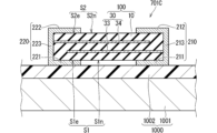
- FIG. 1 is a cross-sectional view illustrating a schematic configuration of a ceramic electronic component according to a first embodiment.
- 2 is a partial cross-sectional view that shows a schematic configuration of an electronic device in which the ceramic electronic component of FIG. 1 is mounted and a conductive resin film is formed with an optimal spread.
- FIG. 3 is a diagram illustrating a case where the conductive resin film spreads less than that in FIG. 2 .
- FIG. 3 is a diagram illustrating a case where the conductive resin film is spread excessively compared to FIG. 2 .
- FIG. 3 is a partial cross-sectional view that illustrates a first step of a method for manufacturing a ceramic electronic component in accordance with the first embodiment.
- FIG. 4 is a partial cross-sectional view that roughly illustrates a second step of the method for manufacturing the ceramic electronic component in accordance with the first embodiment.
- FIG. 4 is a partial cross-sectional view that roughly illustrates a third step in the method for manufacturing the ceramic electronic component according to the first embodiment.
- FIG. 4 is a partial cross-sectional view that roughly illustrates a fourth step in the method for manufacturing the ceramic electronic component according to the first embodiment.
- FIG. 10 is a partial cross-sectional view that roughly illustrates a fifth step in the method for manufacturing the ceramic electronic component according to the first embodiment.
- FIG. 10 is a partial cross-sectional view that illustrates a sixth step in the method for manufacturing the ceramic electronic component according to the first embodiment.
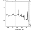
- FIG. 1 is a graph showing an example of the measurement results of X-ray photoelectron spectroscopy (XPS) for the surface of an external electrode of a ceramic electronic component according to an embodiment of the present invention.
- FIG. 11 is a graph showing an example of an XPS measurement result for the surface of an external electrode of a ceramic electronic component of a comparative example.
- FIG. 12 is a graph showing an example of the results of more precise XPS measurement of the dashed line portion EF in FIG. 11 .
- FIG. 12 is a graph showing an example of the results of more precise XPS measurement of the dashed line area EP in FIG. 11 .
- FIG. 2 is a graph showing the distribution range of F/Pt in Table 1.
- 11 is a cross-sectional view illustrating a schematic configuration of a ceramic electronic component according to a second embodiment.
- FIG. 11 is a cross-sectional view illustrating a schematic configuration of a ceramic electronic component according to a third embodiment.
- ⁇ First embodiment> 1 is a cross-sectional view that illustrates a schematic configuration of a ceramic electronic component 701 according to the first embodiment.
- the ceramic electronic component 701 may be a multilayer ceramic electronic component manufactured using multilayer ceramic technology.
- the ceramic electronic component 701 may be a chip-shaped electronic component, such as a chip capacitor.
- the ceramic electronic component 701 has a size of, for example, a length of 1 mm (horizontal dimension in FIG. 1 ), a thickness of 0.1 mm (vertical dimension in FIG. 1 ), and a width of 0.5 mm.
- the ceramic electronic component 701 has a main body 100 and at least one external electrode 200.
- the at least one external electrode 200 is a plurality of external electrodes 200 including a first external electrode 210 and a second external electrode 220.
- the at least one external electrode 200 may include an electrode containing platinum (Pt), which may be an electrode substantially made of Pt, i.e., a Pt electrode.
- Pt platinum
- the material of the at least one external electrode 200 does not necessarily contain Pt, and may be, for example, a material containing at least one of copper, palladium, gold, silver, nickel, tungsten, and molybdenum.
- the external electrode 200 is a Pt electrode will be described in detail below.
- the main body 100 has a first surface S1 and a second surface S2 opposite to the first surface S1 in the thickness direction (vertical direction in the figure).
- the main body 100 also has a third surface S3 connecting the first surface S1 and the second surface S2, and a fourth surface S4 connecting the first surface S1 and the second surface S2.
- the third surface S3 and the fourth surface S4 may be surfaces opposite to each other in the length direction (horizontal direction in the figure) as shown in FIG. 1.
- the main body 100 includes a ceramic portion 10.
- Each of the first surface S1 and the second surface S2 may be a surface made of the ceramic portion 10 as shown in FIG. 1.
- the first surface S1 and the second surface S2 may be a surface of the ceramic portion 10.
- the ceramic portion 10 is typically made of an insulator.
- the ceramic portion 10 is typically an insulator ceramic portion.
- the first external electrode 210 includes a first portion 211 located on the first surface S1 of the main body 100.
- the first external electrode 210 also includes a second portion 212 located on the second surface S2 of the main body 100, and a third portion 213 located on the third surface S3 of the main body 100.
- the second external electrode 220 includes a first portion 221 located on the first surface S1 of the main body 100.
- the second external electrode 220 also includes a second portion 222 located on the second surface S2 of the main body 100 and a fourth portion 223 located on the fourth surface S4 of the main body 100.
- the main body 100 may have at least one first internal electrode layer 33 connected to the third portion 213 of the first external electrode 210.
- the main body 100 may also have at least one second internal electrode layer 34 connected to the fourth portion 223 of the second external electrode 220.
- the fluorine compound 400 is present on the surface of the first portion 211 of the first external electrode 210. In this embodiment, the fluorine compound 400 is also present on the surface of the first portion 221 of the second external electrode 220. In this embodiment, the fluorine compound 400 may also be present on the surface of the second portion 212 of the first external electrode 210 and on the surface of the second portion 222 of the second external electrode 220.
- the first surface S1 of the main body 100 has a first region S1e covered by the external electrode 200 (in this embodiment, the first external electrode 210 and the second external electrode 220) and a second region S1n that is not covered by the external electrode 200.
- the second surface S2 of the main body 100 has a first region S2e that is covered by the external electrode 200 and a second region S2n that is not covered by the external electrode 200.
- the fluorine compound 400 may also be present on the second region S1n of the first surface S1 of the main body 100.
- the fluorine compound 400 may also be present on the second region S2n of the second surface S2 of the main body 100.
- the amount of the fluorine compound 400 per unit area may be lower on the second region S1n than on the first portions 211, 221 of the external electrode 200.
- the amount of the fluorine compound 400 per unit area may also be lower on the second region S2n than on the second portions 212, 222 of the external electrode 200.
- the fluorine compound 400 may not be present in the second region S1n.
- the fluorine compound 400 may not be present in the second region S2n.
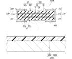
- FIG. 2 is a partial cross-sectional view showing the schematic configuration of electronic device 2101 in which ceramic electronic component 701 (FIG. 1) is mounted.
- Electronic device 2101 includes substrate 800, ceramic electronic component 701, and conductive resin films 921, 922.
- Substrate 800 includes base 801 made of an insulator and wiring parts 803, 804 made of conductors.
- third part 213 of first external electrode 210 of ceramic electronic component 701 is connected to wiring part 803 by conductive resin film 921
- fourth part 223 of second external electrode 220 of ceramic electronic component 701 is connected to wiring part 804 by conductive resin film 922.
- the conductive resin films 921 and 922 are provided to electrically connect the first external electrode 210 and the second external electrode 220 to the wiring portion 803 and the wiring portion 804, respectively, while maintaining high mounting reliability of the ceramic electronic component 701 on the substrate 800.
- the conductive resin films 921 and 922 are formed by applying a liquid resin material and then curing it. Therefore, the spread of each of the conductive resin films 921 and 922 is greatly affected by the wettability of the ceramic electronic component 701 with respect to the liquid resin material.
- the amount of the liquid resin material applied to form each of the conductive resin films 921 and 922 is usually predetermined, and is, for example, about 10 microliters.
- the conductive resin film 921 and the conductive resin film 922 each have an optimal spread. Specifically, the conductive resin film 921 reaches both the first portion 211 of the first external electrode 210 and the substrate 800. Similarly, the protective resin film 912 reaches both the first portion 221 of the second external electrode 220 and the substrate 800. On the other hand, the conductive resin film 921 and the conductive resin film 922 are not in contact with each other on the first surface S1 of the main body 100 and are separated from each other, thereby preventing the first external electrode 210 and the second external electrode 220 from being electrically short-circuited.
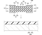
- FIG. 3 is a partial cross-sectional view that shows a schematic configuration of electronic device 2102 in which the spread of conductive resin film 921 and conductive resin film 922 is smaller than that of electronic device 2101 (FIG. 2). Specifically, conductive resin film 921 and conductive resin film 922 do not reach onto first portion 211 of first external electrode 210 and onto first portion 221 of second external electrode 220. In the illustrated example, the spread is even smaller, and conductive resin film 921 and conductive resin film 922 do not reach onto first external electrode 210 and second external electrode 220.
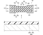
- FIG. 4 is a schematic diagram of an electronic device 2103 in which the conductive resin film 921 and the conductive resin film 922 are excessively extended compared to the electronic device 2101 (FIG. 2).
- the conductive resin films 921 and 922 are excessively extended on the first surface S1 on which the first external electrode 210 and the second external electrode 220 are provided, resulting in a shortage of the amount of the conductive resin films 921 and 922 near the substrate 800, and the conductive resin films 921 and 922 are separated from the substrate 800.
- the conductive resin films 921 and 922 lose their function for electrical connection.
- the extension is even more excessive, and the conductive resin film 921 and the conductive resin film 922 are in contact with each other on the first surface S1, resulting in a defect in which the first external electrode 210 and the second external electrode 220 are electrically shorted to each other.
- FIGS. 5 to 10 are partial cross-sectional views that outline the first to sixth steps of the manufacturing method for ceramic electronic component 701 (FIG. 1).
- ceramic electronic component 701C (FIG. 5) is prepared, which becomes ceramic electronic component 701 (FIG. 1) by providing fluorine compound 400 (FIG. 1). In other words, ceramic electronic component 701C that does not have fluorine compound 400 is manufactured. Ceramic electronic component 701C may be manufactured by a known manufacturing method.
- a surface modification tool 1000 is prepared.
- the tool 1000 has a surface made of a fluorine compound layer 1002 (fluorine compound portion).
- the fluorine compound layer 1002 is supported by a support plate 1001 (support portion).
- the fluorine compound layer 1002 may be made of, for example, Viton (registered trademark) or other fluororesin.
- the tool 1000 may be manufactured, for example, by applying a liquid fluorine elastomer onto the support plate 1001 and then curing the liquid fluorine elastomer to change it into a cured product made of a fluorine compound.
- the fluorine compound layer 1002 is an elastomer layer.
- the ceramic electronic component 701C is placed opposite the fluorine compound layer 1002. Specifically, the first surface S1 on which the first portion 211 of the first external electrode 210 and the first portion 221 of the second external electrode 220 are provided is placed opposite the fluorine compound layer 1002.
- a surface modification process using the fluorine compound layer 1002 as a material source that is, a fluorine attachment process.
- This process can be intensified by heating the fluorine compound layer 1002. Further referring to FIG. 7, this fluorine deposition process results in a ceramic electronic component 701M in which fluorine compound 400 (see FIG. 1) is present on first portion 211 and first portion 221.
- the fluorine compound 400 may also be present on the second region S1n of the first surface S1 of the ceramic portion 10.
- the fluorine compound layer 1002 may also be in contact with the second region S1n, in which case more fluorine compound 400 is formed on the second region S1n. This contact state is easily obtained because the fluorine compound layer 1002 is an elastomer layer, and is easily maintained because the surface of the fluorine compound layer 1002 has adhesiveness.
- the ceramic electronic component 701M is placed opposite the fluorine compound layer 1002. Specifically, the second surface S2 on which the second portion 212 of the first external electrode 210 and the second portion 222 of the second external electrode 220 are provided is placed opposite the fluorine compound layer 1002.
- the second portion 212 of the first external electrode 210 and the second portion 222 of the second external electrode 220 are disposed on the fluorine compound layer 1002. Specifically, a contact state between the second portion 212 of the first external electrode 210 and the second portion 222 of the second external electrode 220 and the fluorine compound layer 1002 is obtained.
- the fluorine compound layer 1002 is an elastomer layer
- the fluorine compound layer 1002 deforms in response to the surfaces of the second portion 212 and the second portion 222, so that the contact state can be obtained over a wider area.
- the surface of the fluorine compound layer 1002 has adhesiveness, so that the contact state can be easily maintained.
- a fluorine attachment process is performed using the fluorine compound layer 1002 as a material source. This process can be intensified by heating the fluorine compound layer 1002. Further referring to FIG. 10, this fluorine deposition process results in a ceramic electronic component 701 in which fluorine compound 400 is present on second portion 212 and second portion 222.
- the fluorine attachment process may be completed at the stage shown in FIG. 7, and the steps shown in FIG. 8 and FIG. 9 may be omitted.
- ceramic electronic component 701M (FIG. 7) is obtained instead of ceramic electronic component 701 as a component for electronic devices.
- the fluorine compound 400 may also be present on the second region S2n of the second surface S2 of the ceramic portion 10.
- the fluorine compound layer 1002 may also be in contact with the second region S2n, in which case more fluorine compound 400 is present on the second region S2n. This contact state is easily obtained because the fluorine compound layer 1002 is an elastomer layer, and is easily maintained because the surface of the fluorine compound layer 1002 has adhesiveness.
- FIG. 11 is a graph showing an example of the XPS measurement results for the surface of the external electrode 200 (specifically, the first portion 211 of the first external electrode 210) for three samples (in other words, for the examples) corresponding to the ceramic electronic component 701.
- the fluorine attachment treatments for the samples in this figure were performed at 80° C. for two hours.
- the dashed line portion EP corresponds to the binding energy of the 4f peak of Pt (platinum) contained in the Pt electrode as the first external electrode 210.
- the dashed line portion EF corresponds to the binding energy of the 1s peak of F (fluorine) contained in the fluorine compound 400 on the surface of the first external electrode 210.
- F/Pt the ratio of the effective peak height of the 1s peak of F to the effective peak height of the 4f peak of Pt. Details of the effective peak height will be described later.
- FIG. 12 is a graph showing an example of the XPS measurement results for the surface of the external electrode 200 (specifically, the first portion 211 of the first external electrode 210) for three samples of the ceramic electronic component 701C (see FIG. 5) that does not have the fluorine compound 400 (see FIG. 1).
- FIG. 12 shows the XPS measurement results for a comparative example that does not have a fluorine adhesion treatment.
- no F 1s peak was observed at the dashed line portion EF. Comparing FIG. 11 with FIG. 12, it is considered that the above-mentioned F/Pt value can be used as an index representing the amount of the fluorine compound 400 on the Pt electrode as the external electrode 200.
- the effective peak area height of F 1s and the effective peak area height of Pt 4f for calculating the ratio F/Pt are specifically calculated as follows. First, referring to the XPS measurement results in FIG. 13, the effective peak height of the F 1s peak is calculated by using the peak height of the flat part adjacent to the 1s peak in the energy region lower than the 1s peak as the background BG. For example, the peak height in the vicinity of 700 eV is used as the background BG.
- the effective peak height is calculated by subtracting the background BG from the maximum 1s peak height of F (for example, any of the peak heights VF1 to VF3).
- the effective peak height of the Pt 4f peak is calculated by using the peak height of the flat area adjacent to the 4f peak in the lower energy region as the background BG. For example, the peak height near 85 eV is used as the background BG.
- the effective peak height is calculated by subtracting the background BG from the maximum Pt 4f peak height (for example, any of the peak heights VP1 to VP3).
- the above XPS was performed using an ESCA-5600ci from ULVAC-PHI Inc.
- a monochromatic 300W Al source was used as the X-ray source.
- the X-ray spot size was 0.5 mm in diameter.
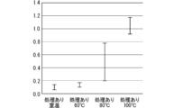
- Table 1 shows the results of investigating the yield rate and F/Pt value of electronic devices (see Figures 2 to 4) equipped with ceramic electronic components without fluorine deposition treatment and with fluorine deposition treatment at room temperature, 60°C, 80°C, and 100°C.
- Figure 15 is a graph showing the distribution range of F/Pt in Table 1.
- the above-mentioned yield rate was calculated by regarding the electronic device obtained by mounting the sample as a good product if it corresponds to electronic device 2001 (Fig. 2), and as a defective product if it corresponds to electronic device 2002 (Fig. 3) or electronic device 2003 (Fig. 4). Note that in the above table, "No F peak" in the F/Pt column indicates that the F 1s peak was not significantly detected.
- the yield rate is improved in the "treated” case compared to the "untreated” case.
- the reason for the low yield rate in the untreated case is believed to be that the surface state of the untreated surface is not controlled, and therefore there is a large variation in wettability with the liquid resin material used to form protective resin film 911 and protective resin film 912 (FIGS. 2 to 4).
- the wettability of the untreated surface is greatly affected by substances (e.g., moisture or organic matter) that are adsorbed onto the surface without any particular control.
- the F/Pt in the "treated” case in Table 1 corresponds to a range of 0.06 to 1.18 (see also FIG. 16).
- the yield rate was higher at 60°C, 80°C, and 100°C than at room temperature.
- F/Pt in these cases corresponded to a range of 0.10 to 1.18 (see also FIG. 16). It can be seen that the yield rate was maximized especially at 80°C.
- F/Pt in this case corresponded to a range of 0.20 to 0.78 (see also FIG. 16).
- the higher the temperature of the fluorine attachment treatment the larger F/Pt becomes, it is considered that the wettability was optimized by setting F/Pt to a value that was neither too large nor too small, and therefore the yield rate was maximized.
- the external electrode 200 may be made of another metal (hereinafter, also referred to as metal M) instead of Pt.
- metal M another metal
- a ratio F/M similar to F/Pt is calculated based on the XPS measurement result by using an appropriate peak of metal M instead of the 4f peak of Pt.
- F/M a ratio having a suitable numerical range as described above is obtained.
- the correction coefficient C can be easily obtained experimentally, for example, by performing a fluorine attachment treatment under common conditions on a plate made of Pt and a plate made of metal M, and then performing XPS. Specifically, the correction coefficient C is determined so that a common peak ratio is obtained under common conditions.
- the metal M is made of an alloy made of elements E A , E B ...
- the effective peak height of the metal M may be calculated from the effective peak height of element E A + the effective peak height of element E B + ....
- the fluorine compound 400 is present on the surfaces of the first portions 211, 221 of the external electrode 200.
- the amount of this fluorine compound 400 it is possible to control the wettability of the first portions 211, 221 of the external electrode 200 with the resin material for forming the conductive resin films 921, 922. This makes it possible to optimize the wettability of the external electrode 200. As a result, it is possible to improve the mounting reliability of the ceramic electronic component 701.
- an insulating resin film having a shape similar to that of the conductive resin films 921, 922 may be used instead of the conductive resin films 921, 922.
- a member for electrically connecting the first external electrode 210 to the wiring portion 803 and a member for electrically connecting the second external electrode 220 to the wiring portion 804 may be further provided.
- These members may be covered with an insulating resin film.
- the insulating resin film is provided to improve the mounting reliability of the ceramic electronic component 701 to the substrate 800.
- the specific purpose of the insulating resin film depends on the specifications of the electronic device 2001, but typically, for the ceramic electronic component 701, it is at least one of protecting the electrical connection points to the substrate 800 and reinforcing the mechanical connection to the substrate 800.
- the insulating resin film when the shape of the insulating resin film corresponds to the shape of the conductive resin films 921 and 922 in FIG. 2, the insulating resin film has an optimal spread.
- the shape of the insulating resin film corresponds to the shape of the conductive resin films 921 and 922 in FIG. 3 or FIG. 4, the parts that should be protected by the insulating resin film are not protected.
- the insulating resin film is preferably made of an insulator, such as epoxy resin.
- the insulating resin film is formed by applying a liquid resin material and then curing it. Therefore, the spread of each insulating resin film is greatly affected by the wettability of the ceramic electronic component 701 with respect to the liquid resin material.
- the amount of liquid resin material applied to form each insulating resin film is usually predetermined, and is, for example, about 10 microliters.
- FIG. 16 is a cross-sectional view that illustrates a schematic configuration of a ceramic electronic component 702 according to the second embodiment.
- the ceramic electronic component 702 has a first external electrode 230 and a second external electrode 240 as at least one external electrode 200, instead of the first external electrode 210 and the second external electrode 220 (FIG. 2).
- the first external electrode 230 is disposed on the first surface S1, and in the illustrated example, is disposed over substantially the entire first surface S1.
- the first external electrode 230 does not need to be disposed on any surface other than the first surface S1.
- the second external electrode 240 is disposed on the second surface S2, and in the illustrated example, is disposed over substantially the entire second surface S2.
- the second external electrode 240 does not need to be disposed on any surface other than the second surface S2.
- the internal electrode layers 33 and 34 are not necessary.
- ⁇ Third embodiment> 17 is a cross-sectional view that roughly illustrates the configuration of a ceramic electronic component 703 according to the present embodiment 3.
- the ceramic electronic component 703 has, as at least one external electrode 200, a first external electrode 250 and a second external electrode 260 instead of the first external electrode 210 and the second external electrode 220 ( FIG. 2 ).
- the first external electrode 210 includes a first portion 251 located on the first surface S1 of the main body 100.
- the first external electrode 210 also includes a second portion 252 located on the second surface S2 of the main body 100, and a third portion 253 located on a portion of the third surface S3 of the main body 100.
- the first portion 251 is disposed over substantially the entire first surface S1.
- the second external electrode 260 is disposed on the second surface S2 away from the first external electrode 250.
- the second external electrode 260 does not need to be disposed on any surface other than the second surface S2.
- the internal electrode layers 33, 34 ( Figure 2) are also not required.
- Ceramic portion 33, 34 First and second internal electrode layers 100: Main body 200: External electrode 210, 230, 250: First external electrode 211, 221, 251: First portion 212, 222, 252: Second portion 213, 253: Third portion 220, 240, 260: Second external electrode 223: Fourth portion 400: Fluorine compound 701-703: Ceramic electronic component 800: Substrate 801: Base portion 803, 804: Wiring portion 921, 922: Conductive resin film 1002: Fluorine compound layer 2101: Electronic device S1-S4: First to fourth surfaces S1e, S2e: First region S1n, S2n: Second region
Landscapes
- Engineering & Computer Science (AREA)
- Power Engineering (AREA)
- Manufacturing & Machinery (AREA)
- Microelectronics & Electronic Packaging (AREA)
- Fixed Capacitors And Capacitor Manufacturing Machines (AREA)
Priority Applications (2)
| Application Number | Priority Date | Filing Date | Title |
|---|---|---|---|
| JP2025509931A JPWO2024202709A1 (https=) | 2023-03-31 | 2024-02-20 | |
| US19/341,536 US20260024704A1 (en) | 2023-03-31 | 2025-09-26 | Ceramic electronic component and method of manufacturing the same |
Applications Claiming Priority (2)
| Application Number | Priority Date | Filing Date | Title |
|---|---|---|---|
| JP2023-058510 | 2023-03-31 | ||
| JP2023058510 | 2023-03-31 |
Related Child Applications (1)
| Application Number | Title | Priority Date | Filing Date |
|---|---|---|---|
| US19/341,536 Continuation US20260024704A1 (en) | 2023-03-31 | 2025-09-26 | Ceramic electronic component and method of manufacturing the same |
Publications (1)
| Publication Number | Publication Date |
|---|---|
| WO2024202709A1 true WO2024202709A1 (ja) | 2024-10-03 |
Family
ID=92905083
Family Applications (1)
| Application Number | Title | Priority Date | Filing Date |
|---|---|---|---|
| PCT/JP2024/006007 Ceased WO2024202709A1 (ja) | 2023-03-31 | 2024-02-20 | セラミック電子部品およびその製造方法 |
Country Status (3)
| Country | Link |
|---|---|
| US (1) | US20260024704A1 (https=) |
| JP (1) | JPWO2024202709A1 (https=) |
| WO (1) | WO2024202709A1 (https=) |
Citations (4)
| Publication number | Priority date | Publication date | Assignee | Title |
|---|---|---|---|---|
| JP2002203737A (ja) * | 2001-01-05 | 2002-07-19 | Murata Mfg Co Ltd | 積層セラミック電子部品及びその製造方法 |
| JP2019175989A (ja) * | 2018-03-28 | 2019-10-10 | 三菱電機株式会社 | 半導体装置 |
| JP2020167379A (ja) * | 2019-03-28 | 2020-10-08 | 太陽誘電株式会社 | 積層セラミックコンデンサおよびその製造方法 |
| JP2022097372A (ja) * | 2020-12-18 | 2022-06-30 | サムソン エレクトロ-メカニックス カンパニーリミテッド. | 積層型電子部品及びその製造方法 |
-
2024
- 2024-02-20 WO PCT/JP2024/006007 patent/WO2024202709A1/ja not_active Ceased
- 2024-02-20 JP JP2025509931A patent/JPWO2024202709A1/ja active Pending
-
2025
- 2025-09-26 US US19/341,536 patent/US20260024704A1/en active Pending
Patent Citations (4)
| Publication number | Priority date | Publication date | Assignee | Title |
|---|---|---|---|---|
| JP2002203737A (ja) * | 2001-01-05 | 2002-07-19 | Murata Mfg Co Ltd | 積層セラミック電子部品及びその製造方法 |
| JP2019175989A (ja) * | 2018-03-28 | 2019-10-10 | 三菱電機株式会社 | 半導体装置 |
| JP2020167379A (ja) * | 2019-03-28 | 2020-10-08 | 太陽誘電株式会社 | 積層セラミックコンデンサおよびその製造方法 |
| JP2022097372A (ja) * | 2020-12-18 | 2022-06-30 | サムソン エレクトロ-メカニックス カンパニーリミテッド. | 積層型電子部品及びその製造方法 |
Also Published As
| Publication number | Publication date |
|---|---|
| JPWO2024202709A1 (https=) | 2024-10-03 |
| US20260024704A1 (en) | 2026-01-22 |
Similar Documents
| Publication | Publication Date | Title |
|---|---|---|
| JP7379899B2 (ja) | セラミック電子部品 | |
| US7764484B2 (en) | Multilayer electronic component and method for manufacturing the same | |
| US10615327B2 (en) | Monolithic ceramic electronic component | |
| JP5246207B2 (ja) | チップ型電子部品 | |
| JP3376970B2 (ja) | セラミック電子部品 | |
| US9536643B2 (en) | Method for manufacturing multilayer electronic component | |
| US6803116B2 (en) | Method of bonding a conductive adhesive and an electrode, and a bonded electrode obtained thereby | |
| US8130484B2 (en) | Monolithic ceramic electronic component and mounting structure thereof | |
| KR101953655B1 (ko) | 적층 세라믹 전자부품 | |
| WO2007007677A1 (ja) | 電子部品、電子部品の実装構造および電子部品の製造方法 | |
| JP7136334B2 (ja) | チップ型セラミック電子部品およびその製造方法 | |
| JP3760770B2 (ja) | 積層セラミック電子部品及びその製造方法 | |
| WO2024202709A1 (ja) | セラミック電子部品およびその製造方法 | |
| US7910402B2 (en) | Semiconductor device and fabrication method thereof | |
| US20090321121A1 (en) | Ceramic multilayer substrate and its manufacturing method | |
| JPH05218137A (ja) | 半導体装置の製造方法 | |
| CN113053602B (zh) | 电阻器组件 | |
| JP6610159B2 (ja) | 薄膜キャパシタ | |
| JP4993545B2 (ja) | 電子部品および電子部品の製造方法 | |
| KR20230121405A (ko) | 저항 부품 | |
| JP4978294B2 (ja) | 半導体装置およびその製造方法 | |
| JPH04273417A (ja) | 積層セラミックコンデンサ | |
| KR20260024341A (ko) | 패키징 기판 및 이를 포함하는 반도체 패키지 | |
| JPH04105310A (ja) | 積層セラミックコンデンサ | |
| JP2025076764A (ja) | 電子部品及び電子部品の製造方法 |
Legal Events
| Date | Code | Title | Description |
|---|---|---|---|
| 121 | Ep: the epo has been informed by wipo that ep was designated in this application |
Ref document number: 24778853 Country of ref document: EP Kind code of ref document: A1 |
|
| ENP | Entry into the national phase |
Ref document number: 2025509931 Country of ref document: JP Kind code of ref document: A |
|
| WWE | Wipo information: entry into national phase |
Ref document number: 2025509931 Country of ref document: JP |
|
| NENP | Non-entry into the national phase |
Ref country code: DE |
|
| 122 | Ep: pct application non-entry in european phase |
Ref document number: 24778853 Country of ref document: EP Kind code of ref document: A1 |