WO2024199766A1 - Absorption increase, efficiency enhancement and spatial light modulation by micro-structuring color conversion layers - Google Patents
Absorption increase, efficiency enhancement and spatial light modulation by micro-structuring color conversion layers Download PDFInfo
- Publication number
- WO2024199766A1 WO2024199766A1 PCT/EP2024/052228 EP2024052228W WO2024199766A1 WO 2024199766 A1 WO2024199766 A1 WO 2024199766A1 EP 2024052228 W EP2024052228 W EP 2024052228W WO 2024199766 A1 WO2024199766 A1 WO 2024199766A1
- Authority
- WO
- WIPO (PCT)
- Prior art keywords
- color conversion
- ink
- conversion layer
- micro
- led
- Prior art date
- Legal status (The legal status is an assumption and is not a legal conclusion. Google has not performed a legal analysis and makes no representation as to the accuracy of the status listed.)
- Ceased
Links
Classifications
-
- C—CHEMISTRY; METALLURGY
- C09—DYES; PAINTS; POLISHES; NATURAL RESINS; ADHESIVES; COMPOSITIONS NOT OTHERWISE PROVIDED FOR; APPLICATIONS OF MATERIALS NOT OTHERWISE PROVIDED FOR
- C09K—MATERIALS FOR MISCELLANEOUS APPLICATIONS, NOT PROVIDED FOR ELSEWHERE
- C09K11/00—Luminescent materials, e.g. electroluminescent or chemiluminescent
- C09K11/02—Use of particular materials as binders, particle coatings or suspension media therefor
- C09K11/025—Use of particular materials as binders, particle coatings or suspension media therefor non-luminescent particle coatings or suspension media
-
- G—PHYSICS
- G03—PHOTOGRAPHY; CINEMATOGRAPHY; ANALOGOUS TECHNIQUES USING WAVES OTHER THAN OPTICAL WAVES; ELECTROGRAPHY; HOLOGRAPHY
- G03F—PHOTOMECHANICAL PRODUCTION OF TEXTURED OR PATTERNED SURFACES, e.g. FOR PRINTING, FOR PROCESSING OF SEMICONDUCTOR DEVICES; MATERIALS THEREFOR; ORIGINALS THEREFOR; APPARATUS SPECIALLY ADAPTED THEREFOR
- G03F7/00—Photomechanical, e.g. photolithographic, production of textured or patterned surfaces, e.g. printing surfaces; Materials therefor, e.g. comprising photoresists; Apparatus specially adapted therefor
- G03F7/0002—Lithographic processes using patterning methods other than those involving the exposure to radiation, e.g. by stamping
-
- H—ELECTRICITY
- H10—SEMICONDUCTOR DEVICES; ELECTRIC SOLID-STATE DEVICES NOT OTHERWISE PROVIDED FOR
- H10H—INORGANIC LIGHT-EMITTING SEMICONDUCTOR DEVICES HAVING POTENTIAL BARRIERS
- H10H20/00—Individual inorganic light-emitting semiconductor devices having potential barriers, e.g. light-emitting diodes [LED]
- H10H20/80—Constructional details
- H10H20/85—Packages
- H10H20/851—Wavelength conversion means
- H10H20/8514—Wavelength conversion means characterised by their shape, e.g. plate or foil
-
- H—ELECTRICITY
- H10—SEMICONDUCTOR DEVICES; ELECTRIC SOLID-STATE DEVICES NOT OTHERWISE PROVIDED FOR
- H10K—ORGANIC ELECTRIC SOLID-STATE DEVICES
- H10K59/00—Integrated devices, or assemblies of multiple devices, comprising at least one organic light-emitting element covered by group H10K50/00
- H10K59/30—Devices specially adapted for multicolour light emission
- H10K59/38—Devices specially adapted for multicolour light emission comprising colour filters or colour changing media [CCM]
-
- H—ELECTRICITY
- H10—SEMICONDUCTOR DEVICES; ELECTRIC SOLID-STATE DEVICES NOT OTHERWISE PROVIDED FOR
- H10H—INORGANIC LIGHT-EMITTING SEMICONDUCTOR DEVICES HAVING POTENTIAL BARRIERS
- H10H20/00—Individual inorganic light-emitting semiconductor devices having potential barriers, e.g. light-emitting diodes [LED]
- H10H20/80—Constructional details
- H10H20/85—Packages
- H10H20/851—Wavelength conversion means
- H10H20/8511—Wavelength conversion means characterised by their material, e.g. binder
-
- H—ELECTRICITY
- H10—SEMICONDUCTOR DEVICES; ELECTRIC SOLID-STATE DEVICES NOT OTHERWISE PROVIDED FOR
- H10H—INORGANIC LIGHT-EMITTING SEMICONDUCTOR DEVICES HAVING POTENTIAL BARRIERS
- H10H20/00—Individual inorganic light-emitting semiconductor devices having potential barriers, e.g. light-emitting diodes [LED]
- H10H20/80—Constructional details
- H10H20/85—Packages
- H10H20/851—Wavelength conversion means
- H10H20/8511—Wavelength conversion means characterised by their material, e.g. binder
- H10H20/8512—Wavelength conversion materials
Definitions
- the field of the DISCLOSURE lies in methods for micro-structuring of color conversion layers.
- the present disclosure relates to micro-structured color conversion layers.
- the present disclosure also relates to an LED device or LED lighting device comprising a micro-structured color conversion layer of the present disclosure.
- the present disclosure also relates to an organic LED device or an organic LED lighting device comprising a micro-structured color conversion layer of the present disclosure.
- the methods as of yet are: increase of thickness of the color conversion layer, increase of QD concentration, introduction of scattering agents (e.g. particles) in the matrix.
- these measures are limited in achieving high absorptances while maintaining high conversion efficiencies.
- Increasing the thickness of the color conversion layer is limited to values of about 5 to 10 um in applications with small pixel sizes like micro LED displays or QD-OLED TVs.
- Increasing the QD concentration can lead to severe QD agglomeration which in turns reduces the efficiency of the light conversion.
- the amount of re-absorbed emission light increases which also limits the light conversion efficiency and leads to higher material costs.
- the present disclosure provides a method of generating a micro-structured color conversion layer, said method comprising the steps of: (1) providing an ink comprising (i) emissive material, (ii) monomers cross-linkable by UV light, visible light, or temperature, (iii) an initiator, and (iv) a solvent, preferably an organic solvent; (2) applying the ink onto a substrate, (3) optional, baking; (4) applying a mold to the ink and carrying out nanoimprint lithography (NIL), wherein the mold has a repetitive pattern, wherein said repetitive pattern is defined by a repetition dimension from about 20 nm to about 10 ⁇ m; (5) curing with UV light, in case monomers cross-linkable by UV light are in the ink; or curing with visible light, in case monomers cross-linkable by visible light are in the ink; or curing with heat, in case
- the present disclosure provides a color conversion layer (CCL) comprising: (a) an emissive material, (b) a polymer matrix, which is preferably optically transparent, and (c) an imprinted microstructure having a repetitive pattern, wherein said repetitive pattern is defined by a repetition dimension from about 20 nm to about 10 ⁇ m.
- CCL color conversion layer
- the present disclosure provides an organic electroluminescent (EL) device comprising a color conversion layer of the present disclosure.
- EL organic electroluminescent
- the present disclosure provides an LED device or LED lighting device comprising: (a) a blue, UV, and/or white LED source, and (b) a color conversion layer of the present disclosure, (c) optionally, a substrate.
- OLED organic LED
- OLED lighting device comprising: (a) a blue, UV, and/or white OLED source, and (b) a color conversion layer of the present disclosure, (c) optionally, a substrate.
- Figures 1A and B show cross-sections of two embodiments of micro-structured color conversion layers (CCL).
- Figure 1A shows the cross-section of an embodiment of a CCL wherein the micro-structure extends through the CCL thickness.
- Figure 1B shows the cross- section of another embodiment of an CCL wherein the micro-structure extends only on the upper surface of the CCL.
- Figure 2 shows SEM micrographs of QD CCLs with three different repetitive patterns with three different lateral sizes produced with the method of the disclosure.
- Figure 3 shows enhancement of emission intensity in QD CCLs with different repetitive patterns produced with the method of the disclosure compared with a CCL of similar thickness but without micro-structuring.
- Figure 4 shows the control on spatial emission distribution profile by micro- structuring QD CCL.
- Figure 4A shows the definition of the angles.
- Figure 4B shows the emission profile of a non-structured QD film, which is a Lambertian emission profile.
- Figure 4C shows the emission profiles of micro-structured QD CCLs of the present disclosure, which are non-Lambertian emission profiles.
- Figure 5 shows a comparison of absorptance and frequency conversion efficiency (FCE) between a non-structured QD CCL and a QD CCL micro-structured with 0.5 um holes.
- Figure 6A shows a scheme of the method of the present disclosure for obtaining one embodiment of an QD CCL.
- Figure 6B shows a scheme of the method of the present disclosure for obtaining another embodiment of an QD CCL.
- Figure 6C shows a scheme for fabricating a soft mold from a solid master mold. DETAILED DESCRIPTION OF THE EMBODIMENTS [0023]
- the present disclosure provides a method of generating a micro- structured color conversion layer.
- Said method comprises the steps of: (1) providing an ink comprising (i) emissive material, (ii) monomers cross-linkable by UV light, visible light, or temperature, (iii) an initiator, and (iv) a solvent, preferably an organic solvent; (2) applying the ink onto a substrate, (3) optional, baking; (4) applying a mold to the ink and carrying out nanoimprint lithography (NIL), wherein the mold has a repetitive pattern, wherein said repetitive pattern is defined by a repetition dimension from about 20 nm to about 10 ⁇ m; (5) curing with UV light, in case monomers cross-linkable by UV light are in the ink; or curing with visible light, in case monomers cross-linkable by visible light are in the ink; or curing with heat, in case monomers cross-linkable by temperature are in the ink; (6) removing the mold and thereby obtaining the micro-structured color conversion layer (CCL), wherein said CCL comprises the emissive material dispersed in
- the emissive material (i) is preferably a photo-luminescent emitter material.
- the emissive material is preferably selected from: (I) quantum dots, (II) perovskite nanocrystals, (III) inorganic phosphor materials, and (IV) organic dyes.
- the quantum dots (I) preferably comprise elements of several groups of the periodic system, such as but not limited to: (i) type II/VI nano-crystalline semiconductor materials, such as CdS, CdSe, CdTe, ZnS, ZnSe, ZnTe, CdSe/ZnS, CdSe/CdS, CdSe/ZnSe, CdTe/CdS, CdTe/ZnS, CdTe/CdS/ZnS, (ii) type III/V nano-crystalline semiconductor materials, such as InP, InAs, GaAs, (iii) group IV ⁇ VI elements, such as PbSe, PbS, PbTe, (iv) group IB ⁇ (III) ⁇ VI elements, such as CuInS 2 , AgInS 2 , Ag 2 Se, Ag 2 S; CuInZnS/ZnS, (v) group IV elements, such as silicon QDs (Si QDs), carbon dots (i QD
- the inorganic phosphor materials (III) can be: - YAG:Ce phosphors, (oxy)nitride phosphors, silicate phosphors, Mn4+-activated fluoride phosphors; and [0031]
- the organic dyes can be fluorescent dyes.
- fluorescent dyes are polycyclic aromatics – naphthalene-, anthracene-, pyrene- and perylene based dyes; coumarin dyes; quinolines; indole- and imidazole based dyes; fluorescein; rhodamines; 4,4-difluoro-4-bora-3a,4a-diaza-s-indacene (BODIPY); naphthoxanthene dyes; phenanthridines; cyanines, phthalocyanines, naphthalocyanines; and oxazine based dyes.
- the monomers (ii) comprised in the ink are cross-linkable by UV light, visible light, or temperature. [0033] Preferably they are selected from monoacrylates, and diacrylates. [0034] In one embodiment, the monomers can be monofunctional or polyfunctional.
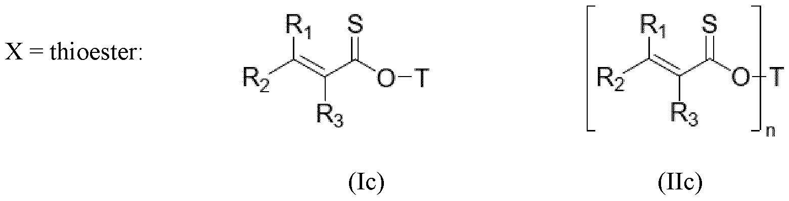
- the monomers can have the general formula I or II wherein: R1 to R3 are each independently selected from hydrogen or C1 to C20 alkyl and can be the same or different; X is a single bond, a C1 to C10 alkylene group, an ether group, a carbonyl group, an ester group, —NH—, an amide group, or a combination thereof; T is selected from a substituted or unsubstituted aliphatic hydrocarbon, a substituted or unsubstituted aliphatic hydrocarbon wherein at least one methylene group is replaced with an ester group, an ether group, a carbonyl group, an amide group, or a combination thereof, a substituted or unsubstituted alkylene oxide moiety, a substituted or unsubstituted polyalkylene oxide moiety, a substituted or unsubstituted heterocyclic moiety, a substituted or unsubstituted alicylic moiety, a substituted or unsubstit
- X X (Ib) (IIb) X [0036]
- T can be: ;
- T can be: .
- R 1 to R 3 are each H.
- the initiator (iii) which is comprised in the ink depends on the monomers (ii) and how they are cross-linked.
- the initiator is a photo UV initiator. Examples are: (dimethylamino)benzophenone.
- the initiator is a thermal initiator.
- examples are: 2,2'-azobisisobutyronitrile (AIBN), tert-butyl peracetate, tert-amyl peroxybenzoate, 1,1'-azobis(cyclohexanecarbonitrile) (ABCN).
- AIBN 2,2'-azobisisobutyronitrile
- tert-butyl peracetate 2,2'-azobisisobutyronitrile
- ABCN 1,1'-azobis(cyclohexanecarbonitrile)
- two components are required: an initiator and a sensitizer.
- initiators are: “Ti-Initiator”: bis(cyclopentadienyl)bis(2,6-difluoro-3-(1H-pyrro; 1-(2,4-Difluorophenyl)-1H- pyrrole titanium complex: , butyltriphenylborate, nBu nBu N + nBu nBu N3B: tetrabutylammonium-butyltrinaphthylborate.
- sensitizers examples are: IRT:1- ⁇ 2,2-bis[4-(diethylamino)phenyl]vinyl ⁇ -3,3-bis[4-(diethylamino)phenyl]propa-2 -ene- 1-ylium p-toluenesulfonate , [0043]
- the solvent (iv) which is comprised in the ink is preferably an organic solvent.
- Solvents are useful for fine control of the layer thickness. Typical solvents have boiling points between about 75°C and 150°C. Examples are propylene glycol methyl ether acetate (PGMEA) and anisole.
- the ink is applied onto the substrate by spin coating, ink-jet printing or drop casting.
- the substrate comprises an adhesion layer.
- the ink is applied onto said adhesion layer.
- the substrate can be glass, such as float glass, borosilicate glass.
- the substrate can be quartz glass, sapphire glass, or a polymer sheet. Examples for polymer sheets are polyethylene terephthalate (PET), polytetrafluoroethylene (PTFE), polyimide (PI).
- PET polyethylene terephthalate
- PTFE polytetrafluoroethylene
- PI polyimide
- the adhesion layer can be a commercially available adhesion layer.
- step (3) baking is carried out.
- baking at temperatures in the range from about 50°C and 150°C, preferably about 80-120°C, for about 1 to 20 minutes, preferably 3 to 10 minutes.
- Baking can be carried out to remove the excess of solvent and to homogenize / smooth the ink before applying the mold, preferably the soft mold.
- the mold in step (4) is a soft mold.
- the soft mold is preferably made of - silicone, such as soft or hard polydimethylsiloxane (PDMS), - fluorinated materials, such as polytetrafluorethylene (PTFE), Teflon, ethylene tetrafluorethylene (ETFE), photocurable fluoropolymers, - photocurable polyurethanes such as polyurethaneacrylate - UV-curable inorganic–organic hybrid polymers such as Ormostamp, Ormocomp.
- PDMS polydimethylsiloxane
- PTFE polytetrafluorethylene
- ETFE ethylene tetrafluorethylene
- photocurable fluoropolymers such as polyurethaneacrylate - UV-curable inorganic–organic hybrid polymers such as Ormostamp, Ormocomp.
- the “mold”, which can also be called “stamp” or “template”, used in step (4) has the inverse of the desired (micro-)structure on its surface.
- a “soft mold” or “soft stamp” or “soft template” is a flexible sheet which has the inverse of the desired (micro-)structure on its surface. The soft mold is used for imprinting said micro- structure.
- a soft mold or stamp is usually flexible to conform to the surface of the substrate and can be transparent to UV or visible light to enable curing through the stamp. The soft mold is usually reusable.
- the soft mold is generated or fabricated from a master mold.
- the master mold or master stamp is a solid mold typically made of Si or Ni metal.
- the steps for fabricating a soft mold which is made of silicone can be: (1) providing an NIL master mold; (2) depositing silicone resin onto the master mold, such as by drop casting or spin-coating; (3) UV curing the silicone resin; and (4) releasing the soft mold. See also Figure 6C.
- the microstructure comprises a repetitive pattern.
- the repetitive pattern is defined by a repetition dimension from about 20 nm to about 10 ⁇ m, preferably 100 nm to 2 ⁇ m.
- the repetitive pattern comprises elements, for example lines, holes, pillars, cones, truncated cones, pyramids, truncated pyramids, rings, prisms and/or cuboids.
- the repetitive pattern is a periodic pattern.
- Said periodic pattern can have a lattice parameter in the range from about 20 nm to about 10 ⁇ m.
- the repetitive pattern is a periodic structure or pattern based on either hexagonal (a), square (b), rectangular (c), or oblique (d) packing of said elements, wherein a and b are in the range from about 20 nm to about 10 ⁇ m and theta ( ⁇ ) is in the range from about 10° to about 120°, as exemplarily illustrated by any of the following representations, with a dot depicting an individual element of said repetitive pattern, preferably said periodic pattern:
- the thickness of the color conversion layer is preferably in the range from about 0.5 ⁇ m to about 500 ⁇ m, preferably about 0.5 ⁇ m to about 100 ⁇ m.
- the thickness of the CCL is in the range from about 0.5 ⁇ m to about 20 ⁇ m, preferably about 0.5 ⁇ m to about 10 ⁇ m.
- the microstructure is preferably imprinted throughout the whole layer.
- the thickness of the CCL is in the range from about 50 ⁇ m to about 500 ⁇ m, preferably about 50 ⁇ m to about 100 ⁇ m.
- the microstructure is preferably imprinted in the upper part of the layer, preferably the upper 0.5 ⁇ m to 10 ⁇ m of the layer.
- a master structure preferably a spacer mask, is used.
- the method of the disclosure comprises the following further steps after step (1): (1-1) defining a master structure on a substrate, preferably by using a spacer mask, wherein said substrate preferably comprises an adhesion layer and the master structure is defined on top of the adhesion layer; (1-2) filling the ink into the master structure, (1-3) optionally, evaporating the solvent from the ink, either by baking or by drying at room temperature; (1-4) curing the ink within the master structure, with UV light, in case monomers cross- linkable by UV light are in the ink; or with visible light, in case monomers cross- linkable by visible light are in the ink; or with heat, in case monomers cross-linkable by temperature are in the ink; and (1-5) obtaining a master-structured color conversion layer; and which comprises step (2a) instead of step (2): (2a) applying the ink onto the master-structured color conversion layer which was obtained in step (1-4), preferably by ink-jet-printing, spin coating or
- step (1-3) the baking is carried out at temperatures in the range from about 50°C to about 150°C, preferably from about 80°C to about 120°C. The drying at room temperature is carried out for about 1 to 20 hours, preferably about 3 to 15 hours.
- step (1-5) a master-structured color conversion layer is obtained as an intermediate product before the micro-structuring.
- One of the purposes of the master structure is to define the areas in which the color conversion takes place.
- These areas can either be individual pixels of a display with lateral sizes between about 0.5 um to about 500 um, preferably about 3 ⁇ m to about 100 ⁇ m; or be the color conversion layer on top of a backlight LED with lateral sizes of about 0.05 mm to 10 mm, preferably about 0.1 mm to 5 mm.
- the method comprises the following steps: (1) providing an ink comprising (i) emissive material, (ii) monomers cross-linkable by UV light, visible light, or temperature, (iii) an initiator, and (iv) a solvent, preferably an organic solvent; (1-1) defining a master structure on a substrate, preferably by using a spacer mask, wherein said substrate preferably comprises an adhesion layer and the master structure is defined on top of the adhesion layer; (1-2) filling the ink into the master structure, (1-3) optionally, evaporating the solvent from the ink, either by baking or by drying at room temperature; (1-4) curing the ink within the master structure, with UV light, in case monomers cross- linkable by UV light are in the ink; or with visible light, in case monomers cross- linkable by visible light are in the ink; or with heat, in case monomers cross-linkable by temperature are in the ink; and (1-5) obtaining a master-structured color
- the method is in particular suitable for obtaining CCLs with a thickness in the range from about 50 ⁇ m to about 500 ⁇ m, preferably about 50 ⁇ m to about 100 ⁇ m, wherein the microstructure is preferably imprinted in the upper part of the layer, preferably the upper 0.5 ⁇ m to 10 ⁇ m of the layer.
- the master structure is preferably a spacer mask.
- the spacer mask is not removed in step (6) and it stays. In embodiments, where the spacer mask is not removed in can serve define grooves which can be filled with emissive material, such as QD, and separated by non-transmissive walls to form a pixel pattern.
- the spacer mask can be defined by other lithography technique and materials, e.g. photolithography.
- the color conversion layer comprises: (a) an emissive material, (b) a polymer matrix, and (c) an imprinted microstructure having a repetitive pattern, wherein said repetitive pattern is defined by a repetition dimension from about 20 nm to about 10 ⁇ m.
- the color conversion layer of the present disclosure has at least one of the following characteristics, more preferably two of the following characteristics or even all three of the following characteristics: [0076] The CCL exhibits increased absorptance. [0077] The CCL shows increased light outcoupling.
- the CCL has a modified non-Lambertian spatial emission profile.
- the emissive material (a) of the CCL is preferably a photo- luminescent emitter material.
- the emissive material is preferably selected from: (I) quantum dots, (II) perovskite nanocrystals, (III) inorganic phosphor materials, and (IV) organic dyes.
- the quantum dots (I) preferably comprise elements of several groups of the periodic system, such as but not limited to: (i) type II/VI nano-crystalline semiconductor materials, such as CdS, CdSe, CdTe, ZnS, ZnSe, ZnTe, CdSe/ZnS, CdSe/CdS, CdSe/ZnSe, CdTe/CdS, CdTe/ZnS, CdTe/CdS/ZnS, (ii) type III/V nano-crystalline semiconductor materials, such as InP, InAs, GaAs, (iii) group IV ⁇ VI elements, such as PbSe, PbS, PbTe, (iv) group IB ⁇ (III) ⁇ VI elements, such as CuInS 2 , AgInS 2 , Ag 2 Se, Ag 2 S; CuInZnS/ZnS, (v) group IV elements, such as silicon QDs (Si QDs), carbon dots (i QD
- the inorganic phosphor materials (III) can be: - YAG:Ce phosphors, (oxy)nitride phosphors, silicate phosphors, Mn4+-activated fluoride phosphors; and [0084]
- the organic dyes can be fluorescent dyes.
- fluorescent dyes are polycyclic aromatics – naphthalene-, anthracene-, pyrene- and perylene based dyes; coumarin dyes; quinolines; indole- and imidazole based dyes; fluorescein; rhodamines; 4,4-difluoro-4-bora-3a,4a-diaza-s-indacene (BODIPY); naphthoxanthene dyes; phenanthridines; cyanines, phthalocyanines, naphthalocyanines; and oxazine based dyes.
- the polymer matrix (b) of the CCL is preferably optically transparent.
- the polymer matrix has good optical transparency in the visible range.
- the polymer matrix has preferably sufficient thermal stability to tolerate the respective operation temperatures (about 120 °C).
- the polymer matrix can have low O2 permeability.
- the polymer matrix is preferably an acrylic matrix.
- the CCL has an imprinted micro-structure having a repetitive pattern (iii).
- the repetitive pattern is defined by a repetition dimension from about 20 nm to about 10 ⁇ m, preferably 100 nm to 2 ⁇ m.
- the repetitive pattern comprises elements, such as lines, holes, pillars, cones, truncated cones, pyramids, truncated pyramids, rings, prisms and/or cuboids.
- the repetitive pattern is a periodic pattern. Said periodic pattern can have a lattice parameter in the range from about 20 nm to about 10 ⁇ m.
- the repetitive pattern is a periodic structure or pattern based on either hexagonal (a), square (b), rectangular (c), or oblique (d) packing of said elements, wherein a and b are in the range from about 20 nm to about 10 ⁇ m and theta ( ⁇ ) is in the range from about 10° to about 120°, as exemplarily illustrated by any of the following representations, with a dot depicting an individual element of said repetitive pattern, preferably said periodic pattern:
- the CCL comprises different imprinted micro-structures, such as microstructures with curved surfaces and/or irregular shapes where the sides and interior angles are not all the same, having a repetitive pattern.
- the thickness of the color conversion layer is preferably in the range from about 0.5 ⁇ m to about 500 ⁇ m, preferably about 0.5 ⁇ m to about 100 ⁇ m.
- the thickness of the CCL is in the range from about 0.5 ⁇ m to about 20 ⁇ m, preferably about 0.5 ⁇ m to about 10 ⁇ m.
- the microstructure is preferably imprinted throughout the whole layer.
- the thickness of the CCL is in the range from about 50 ⁇ m to about 500 ⁇ m, preferably about 50 ⁇ m to about 100 ⁇ m.
- the microstructure is preferably imprinted in the upper part of the layer, preferably the upper 0.5 ⁇ m to 10 ⁇ m of the layer.
- the CCL can further comprise a master structure, preferably a spacer mask.
- the color conversion layer is obtained by a method of the present disclosure.
- the present disclosure provides an organic electroluminescent (EL) device comprising a color conversion layer of the present disclosure.
- EL organic electroluminescent
- the present disclosure provides an LED device or LED lighting device comprising: (a) a blue, UV, and/or white LED source, and (b) a color conversion layer of the present disclosure, (c) optionally, a substrate.
- the LED device or the LED lighting device is preferably a backlight LED, mini- backlight LED, micro-LED array or display.
- the LED device or LED lighting device is a micro LED array display, a micro LED display, an LED backlight display, a LCD display, a micro display in wearable augmented reality glasses, in mobile devices, or in camera.
- the present disclosure provides an organic LED (OLED) device or OLED lighting device comprising: (a) a blue, UV, and/or white OLED source, and (b) a color conversion layer of the present disclosure, (c) optionally, a substrate.
- OLED device or the OLED lighting device is preferably a micro-OLED array or display.
- the OLED device or OLED lighting device is an OLED TV display, a micro OLED array display, a micro OLED display, an OLED backlight display, a OLCD display, a micro display in wearable augmented reality glasses, in mobile devices, or in camera [00106] Note that the present technology can also be configured as described below.
- a method of generating a micro-structured color conversion layer comprising the steps of: (1) providing an ink comprising (i) emissive material, (ii) monomers cross-linkable by UV light, visible light, or temperature, (iii) an initiator, and (iv) a solvent, preferably an organic solvent; (2) applying the ink onto a substrate, preferably by ink-jet printing, spin coating or drop casting, wherein said substrate preferably comprises an adhesion layer and the ink is applied onto said adhesion layer; (3) optional, baking; (4) applying a mold to the ink and carrying out nanoimprint lithography (NIL), wherein the mold has a repetitive pattern, wherein said repetitive pattern is defined by a repetition dimension from about 20 nm to about 10 ⁇ m; (5) curing with UV light, in case monomers cross-linkable by UV light are in the ink; or curing with visible light, in case monomers cross-linkable by visible light are in the ink; or curing with heat, in case mono
- the repetitive pattern comprises elements, such as lines, holes, pillars, cones, truncated cones, pyramids, truncated pyramids, rings, prisms and/or cuboids.
- the mold applied in step (4) is a soft mold, which is preferably made of silicone, fluorinated materials, photocurable polyurethanes or UV-curable inorganic-organic hybrid polymers, and/or which is preferably generated from a master mold.
- the CCL has a thickness in the range from about 0.5 ⁇ m to about 500 ⁇ m, preferably about 0.5 ⁇ m to about 100 ⁇ m.
- the thickness of the CCL is in the range from about 0.5 ⁇ m to about 20 ⁇ m, preferably about 0.5 ⁇ m to about 10 ⁇ m, and wherein the microstructure is imprinted throughout the whole layer.
- the thickness of the CCL is in the range from about 50 ⁇ m to about 500 ⁇ m, preferably about 50 ⁇ m to about 100 ⁇ m, and wherein the microstructure is imprinted in the upper part of the layer, preferably the upper 0.5 ⁇ m to 10 ⁇ m of the layer.
- step (1) (1-1) defining a master structure on a substrate, preferably by using a spacer mask, wherein said substrate preferably comprises an adhesion layer and the master structure is defined on top of the adhesion layer; (1-2) filling the ink into the master structure, (1-3) optionally, evaporating the solvent from the ink, either by baking or drying at room temperature; (1-4) curing the ink within the master structure, with UV light, in case monomers cross-linkable by UV light are in the ink; or with visible light, in case monomers cross-linkable by visible light are in the ink; or with heat, in case monomers cross- linkable by temperature are in the ink; and (1-5) obtaining a master-structured color conversion layer; and which comprises step (2a) instead of step (2): (2a) applying the ink onto the master-structured color conversion layer obtained in step (1-5), preferably by ink-jet printing, spin coating or drop casting; and wherein, optionally
- the emissive material (i) is a photo- luminescent emitter material, which is preferably selected from: (I) quantum dots, which preferably comprise elements of several groups of the periodic system, such as but not limited to: (i) type II/VI nano-crystalline semiconductor materials, such as CdS, CdSe, CdTe, ZnS, ZnSe, ZnTe, CdSe/ZnS, CdSe/CdS, CdSe/ZnSe, CdTe/CdS, CdTe/ZnS, CdTe/CdS/ZnS, (ii) type III/V nano-crystalline semiconductor materials, such as InP, InAs, GaAs, (iii) group IV ⁇ VI elements, such as PbSe, PbS, PbTe, (iv) group IB ⁇ (III) ⁇ VI elements, such as CuInS2, AgInS2, Ag2Se,
- polycyclic aromatics naphthalene-, anthracene-, pyrene- and perylene based dyes; coumarin dyes; quinolines; indole- and imidazole based dyes; fluorescein; rhodamines; 4,4-difluoro-4-bora-3a,4a-diaza-s-indacene (BODIPY); naphthoxanthene dyes; phenanthridines; cyanines, phthalocyanines, naphthalocyanines; oxazine based dyes.
- a color conversion layer comprising (a) an emissive material, (b) a polymer matrix, which is preferably optically transparent, and (c) an imprinted microstructure having a repetitive pattern, wherein said repetitive pattern is defined by a repetition dimension from about 20 nm to about 10 ⁇ m.
- the repetitive pattern comprises elements, such as lines, holes, pillars, cones, truncated cones, pyramids, truncated pyramids, rings, prisms and/or cuboids.
- the emissive material (a) is a photo-luminescent emitter material, which is preferably selected from: (I) quantum dots, which preferably comprise elements of several groups of the periodic system, such as but not limited to: (i) type II/VI nano-crystalline semiconductor materials, such as CdS, CdSe, CdTe, ZnS, ZnSe, ZnTe, CdSe/ZnS, CdSe/CdS, CdSe/ZnSe, CdTe/CdS, CdTe/ZnS, CdTe/CdS/ZnS, (ii) type III/V nano-crystalline semiconductor materials, such as InP, InAs, GaAs, (iii) group IV ⁇ VI elements, such as PbSe, PbS, PbTe, (iv) group IB ⁇ (III) ⁇ VI elements, such as CuInS2, AgInS2, Ag2S
- quantum dots which preferably comprise elements of several groups of the periodic system
- polycyclic aromatics naphthalene-, anthracene-, pyrene- and perylene based dyes; coumarin dyes; quinolines; indole- and imidazole based dyes; fluorescein; rhodamines; 4,4-difluoro-4-bora-3a,4a-diaza-s-indacene (BODIPY); naphthoxanthene dyes; phenanthridines; cyanines, phthalocyanines, naphthalocyanines; oxazine based dyes; and/or the matrix (b) is an acrylic matrix; and/or wherein the matrix (b) is optically transparent.
- An organic electroluminescent (EL) device comprising a color conversion layer of any one of (10) to (17).
- An LED device or LED lighting device comprising (a) a blue, UV, and/or white LED source, and (b) a color conversion layer of any one of (10) to (17), (c) optionally, a substrate, wherein the LED device or the LED lighting device is preferably a backlight LED, a mini- backlight LED, micro-LED array or display.
- An organic LED (OLED) device or OLED lighting device comprising (a) a blue, UV, and/or white OLED source, and (b) a color conversion layer of any one of (10) to (17), (c) optionally, a substrate, wherein the OLED device or the OLED lighting device is preferably a micro-OLED array or display.
- NIL has the advantage of being a simple and cheap method with the possibility of easy up-scaling. Furthermore, it avoids the use of harsh process conditions as they are often applied in photolithography, which can damage sensitive materials, as e.g. QDs are.
- QD CCLs with flat surface i.e. without micro-structure, as in the prior art
- QD CCLs with flat surface usually exhibit a Lambertian emission profile.
- a modified emission profile as it can be achieved with the method of the disclosure and the micro-structured CCLs of the disclosure, are advantagous.
- an emission profile which is narrower can increase the coupling efficiency of micro-displays with receiving optics with low acceptance angles (e.g. AR glasses).
- a broader emission profile can be advantagous for example for TV backlights to reduce the number of LEDs needed for a homogenous illumination of the screen.
- the main advantages of the micro-structuring of CCLs of the disclosure are as follows: [00112] Increase of absorptance: By microstructuring the CCLs, the absorptance can be drastically increased without sacrificing the conversion efficiency. Thereby, also technical requirements (i.e. limited thickness of CCLs) can be fullfilled. In addition, the absorptance increase can also lead to a cost reduction of the CCLs, as much less material (both QDs and matrix) are needed to reach equal absorptances.
- Increase of light outcoupling The microstructuring leads to increased light outcoupling as more light, which would undergo total internal reflection in the case of an unstructured film, can exit the micro-structured film due to modified geometry (changed angle) of the film surface.
- Spatial emission profile The spatial emission profile of the micro-structured films is modified by the introduction of vertical or slanted surface parts. Furthermore, micro-structuring of the film surface with repetitive structures leads to ligth diffraction, which enables the modulation of the spatial emission profile.
- micro-structured QD CCLs with repetitive patterns of lines, holes and pillars were obtained. See Figure 2.
- the QD CCL comprises about 10 wt.-% of SiO 2 shelled CdSe QDs as color converters embedded in optically transparent, acrylic matrix material. After imprinting, the films were 0.7 to 2 um thick and exhibited drastically enhanced absorptance and conversion efficiency over the films witout the structures (thickness 1 ⁇ m). Besides, a modulation of spatial ligth emission profile was observed.
Landscapes
- Chemical & Material Sciences (AREA)
- Physics & Mathematics (AREA)
- General Physics & Mathematics (AREA)
- Engineering & Computer Science (AREA)
- Materials Engineering (AREA)
- Organic Chemistry (AREA)
- Electroluminescent Light Sources (AREA)
Abstract
The field of the DISCLOSURE lies in methods for micro-structuring of color conversion layers. The present disclosure relates to micro-structured color conversion layers. The present disclosure also relates to an LED device or LED lighting device comprising a micro-structured color conversion layer of the present disclosure. The present disclosure also relates to an organic LED device or an organic LED lighting device comprising a micro-structured color conversion layer of the present disclosure.
Description
Sony Semiconductor Solutions Corporation et al. ABSORPTION INCREASE, EFFICIENCY ENHANCEMENT AND SPATIAL LIGHT MODULATION BY MICRO-STRUCTURING COLOR CONVERSION LAYERS BACKGROUND [0001] The field of the DISCLOSURE lies in methods for micro-structuring of color conversion layers. [0002] The present disclosure relates to micro-structured color conversion layers. [0003] The present disclosure also relates to an LED device or LED lighting device comprising a micro-structured color conversion layer of the present disclosure. The present disclosure also relates to an organic LED device or an organic LED lighting device comprising a micro-structured color conversion layer of the present disclosure. DESCRIPTION OF THE RELATED ART [0004] The “background” description provided herein is for the purpose of generally presenting the context of the disclosure. Work of the presently named inventors, to the extent it is described in this background section, as well as aspects of the description which may not otherwise qualify as prior art at the time of filing, are neither expressly or impliedly admitted as prior art against the present disclosure. [0005] Color conversion layers or films as they are applied, for example, in emissive color filters, in on-LED-chip conversion layers or color enhancement films, e.g. quantum dot (QD) color conversion or color enhancement layers should ideally exhibit high light absorptance, high conversion efficiencies and a specific spatial light emission profile at, in many cases, comparably low thicknesses. [0006] In order to increase the absorptance of QD color conversion films the methods as of yet are: increase of thickness of the color conversion layer, increase of QD concentration, introduction of scattering agents (e.g. particles) in the matrix. However, these measures are limited in achieving high absorptances while maintaining high conversion efficiencies. Increasing the thickness of the color conversion layer is limited to values of about 5 to 10 um in applications with small pixel sizes like micro LED displays or QD-OLED TVs. Increasing the QD concentration can lead to severe QD agglomeration which in turns reduces the efficiency of the light conversion. Furthermore, with increasing QD concentration also the amount of re-absorbed emission light increases which also limits the light conversion
efficiency and leads to higher material costs. The introduction of scattering particles can enhance the absorptance of the films by increasing the path length of excitation light in the films. However, this approach only leads to limited success as it also has a detrimental effect on the light conversion efficiencies of the films. SUMMARY [0007] In the following, the elements of the invention will be described. These elements are listed with specific embodiments, however, it should be understood that they may be combined in any manner and in any number to create additional embodiments. The variously described examples and preferred embodiments should not be construed to limit the present invention to only the explicitly described embodiments. This description should be understood to support and encompass embodiments which combine two or more of the explicitly described embodiments or which combine the one or more of the explicitly described embodiments with any number of the disclosed and/or preferred elements. Furthermore, any permutations and combinations of all described elements in this application should be considered disclosed by the description of the present application unless the context indicates otherwise. [0008] The present disclosure provides a method of generating a micro-structured color conversion layer, said method comprising the steps of: (1) providing an ink comprising (i) emissive material, (ii) monomers cross-linkable by UV light, visible light, or temperature, (iii) an initiator, and (iv) a solvent, preferably an organic solvent; (2) applying the ink onto a substrate, (3) optional, baking; (4) applying a mold to the ink and carrying out nanoimprint lithography (NIL), wherein the mold has a repetitive pattern, wherein said repetitive pattern is defined by a repetition dimension from about 20 nm to about 10 µm;
(5) curing with UV light, in case monomers cross-linkable by UV light are in the ink; or curing with visible light, in case monomers cross-linkable by visible light are in the ink; or curing with heat, in case monomers cross-linkable by temperature are in the ink; (6) removing the mold and thereby obtaining the micro-structured color conversion layer (CCL), wherein said CCL comprises the emissive material dispersed in a polymer matrix formed from the monomers, and wherein said CCL has an imprinted microstructure, wherein said microstructure comprises the repetitive pattern being defined by a repetition dimension from about 20 nm to about 10 µm. [0009] The present disclosure provides a color conversion layer (CCL) comprising: (a) an emissive material, (b) a polymer matrix, which is preferably optically transparent, and (c) an imprinted microstructure having a repetitive pattern, wherein said repetitive pattern is defined by a repetition dimension from about 20 nm to about 10 µm. [0010] The present disclosure provides an organic electroluminescent (EL) device comprising a color conversion layer of the present disclosure. [0011] The present disclosure provides an LED device or LED lighting device comprising: (a) a blue, UV, and/or white LED source, and (b) a color conversion layer of the present disclosure, (c) optionally, a substrate. [0012] The present disclosure provides an organic LED (OLED) device or OLED lighting device comprising: (a) a blue, UV, and/or white OLED source, and (b) a color conversion layer of the present disclosure, (c) optionally, a substrate. [0013] The foregoing paragraphs have been provided by way of general introduction and are not intended to limit the scope of the following claims. The described embodiments, together
with further advantages, will be best understood by reference to the following detailed description taken in conjunction with the accompanying drawings. BRIEF DESCRIPTION OF THE DRAWINGS [0014] A more complete appreciation of the disclosure and many of the attendant advantages thereof will be readily obtained as the same becomes better understood by reference to the following detailed description when considered in connection with the accompanying drawings, wherein: [0015] Figures 1A and B show cross-sections of two embodiments of micro-structured color conversion layers (CCL). Figure 1A shows the cross-section of an embodiment of a CCL wherein the micro-structure extends through the CCL thickness. Figure 1B shows the cross- section of another embodiment of an CCL wherein the micro-structure extends only on the upper surface of the CCL. [0016] Figure 2 shows SEM micrographs of QD CCLs with three different repetitive patterns with three different lateral sizes produced with the method of the disclosure. [0017] Figure 3 shows enhancement of emission intensity in QD CCLs with different repetitive patterns produced with the method of the disclosure compared with a CCL of similar thickness but without micro-structuring. [0018] Figure 4 shows the control on spatial emission distribution profile by micro- structuring QD CCL. Figure 4A shows the definition of the angles. Figure 4B shows the emission profile of a non-structured QD film, which is a Lambertian emission profile. Figure 4C shows the emission profiles of micro-structured QD CCLs of the present disclosure, which are non-Lambertian emission profiles. [0019] Figure 5 shows a comparison of absorptance and frequency conversion efficiency (FCE) between a non-structured QD CCL and a QD CCL micro-structured with 0.5 um holes. [0020] Figure 6A shows a scheme of the method of the present disclosure for obtaining one embodiment of an QD CCL. [0021] Figure 6B shows a scheme of the method of the present disclosure for obtaining another embodiment of an QD CCL. [0022] Figure 6C shows a scheme for fabricating a soft mold from a solid master mold. DETAILED DESCRIPTION OF THE EMBODIMENTS [0023] As discussed above, the present disclosure provides a method of generating a micro- structured color conversion layer.
[0024] Said method comprises the steps of: (1) providing an ink comprising (i) emissive material, (ii) monomers cross-linkable by UV light, visible light, or temperature, (iii) an initiator, and (iv) a solvent, preferably an organic solvent; (2) applying the ink onto a substrate, (3) optional, baking; (4) applying a mold to the ink and carrying out nanoimprint lithography (NIL), wherein the mold has a repetitive pattern, wherein said repetitive pattern is defined by a repetition dimension from about 20 nm to about 10 µm; (5) curing with UV light, in case monomers cross-linkable by UV light are in the ink; or curing with visible light, in case monomers cross-linkable by visible light are in the ink; or curing with heat, in case monomers cross-linkable by temperature are in the ink; (6) removing the mold and thereby obtaining the micro-structured color conversion layer (CCL), wherein said CCL comprises the emissive material dispersed in a polymer matrix formed from the monomers, and wherein said CCL has an imprinted microstructure, wherein said microstructure comprises the repetitive pattern being defined by a repetition dimension from about 20 nm to about 10 µm. [0025] In accordance with the present disclosure, the terms “color conversion filter”, “color conversion film”, and “color conversion layer” are used interchangeably. [0026] The emissive material (i) is preferably a photo-luminescent emitter material. [0027] The emissive material is preferably selected from: (I) quantum dots, (II) perovskite nanocrystals, (III) inorganic phosphor materials, and (IV) organic dyes. [0028] The quantum dots (I) preferably comprise elements of several groups of the periodic system, such as but not limited to: (i) type II/VI nano-crystalline semiconductor materials,
such as CdS, CdSe, CdTe, ZnS, ZnSe, ZnTe, CdSe/ZnS, CdSe/CdS, CdSe/ZnSe, CdTe/CdS, CdTe/ZnS, CdTe/CdS/ZnS, (ii) type III/V nano-crystalline semiconductor materials, such as InP, InAs, GaAs, (iii) group IV−VI elements, such as PbSe, PbS, PbTe, (iv) group IB−(III)−VI elements, such as CuInS2, AgInS2, Ag2Se, Ag2S; CuInZnS/ZnS, (v) group IV elements, such as silicon QDs (Si QDs), carbon dots (C-dots), graphene QDs (GQDs). [0029] The perovskite nanocrystals (II) can be: - Pb-based CsPbX3; (CH3NH3)PbX3, wherein X = Cl, Br, I, or their halide mixtures, - Sn-based CsSnX3, wherein X = Cl, Cl0.5Br0.5, Br, Br0.5I0.5, I, - Ge-based (RbxCs1-x)GeBr3 ; CsGe(BrxCl1-x)3; CH3NH3GeX3, wherein X = Cl, Br, I, - Bi-based CsA3Bi2X9, wherein X=Cl, Br, I; A=CH3NH3; (NH4)3Bi2I9; (CH3NH3)3(Bi2I9), - Sb-based (NH4)3Sb2IxBr9-x (0<x<9); (CH3NH3)3Sb2I9 ; Cs3Sb2I9, - InAg-based Cs2InAgCl6. [0030] The inorganic phosphor materials (III) can be: - YAG:Ce phosphors, (oxy)nitride phosphors, silicate phosphors, Mn4+-activated fluoride phosphors; and [0031] The organic dyes can be fluorescent dyes. Examples for fluorescent dyes are polycyclic aromatics – naphthalene-, anthracene-, pyrene- and perylene based dyes; coumarin dyes; quinolines; indole- and imidazole based dyes; fluorescein; rhodamines; 4,4-difluoro-4-bora-3a,4a-diaza-s-indacene (BODIPY); naphthoxanthene dyes; phenanthridines; cyanines, phthalocyanines, naphthalocyanines; and oxazine based dyes. [0032] The monomers (ii) comprised in the ink are cross-linkable by UV light, visible light, or temperature. [0033] Preferably they are selected from monoacrylates, and diacrylates.
[0034] In one embodiment, the monomers can be monofunctional or polyfunctional. The monomers can have the general formula I or II
 wherein: R1 to R3 are each independently selected from hydrogen or C1 to C20 alkyl and can be the same or different; X is a single bond, a C1 to C10 alkylene group, an ether group, a carbonyl group, an ester group, —NH—, an amide group, or a combination thereof; T is selected from a substituted or unsubstituted aliphatic hydrocarbon, a substituted or unsubstituted aliphatic hydrocarbon wherein at least one methylene group is replaced with an ester group, an ether group, a carbonyl group, an amide group, or a combination thereof, a substituted or unsubstituted alkylene oxide moiety, a substituted or unsubstituted polyalkylene oxide moiety, a substituted or unsubstituted heterocyclic moiety, a substituted or unsubstituted alicylic moiety, a substituted or unsubstituted aromatic hydrocarbon group, an organic siloxane moiety, or a combination thereof; n is an integer of greater than 1 and less than or equal to 4. [0035] For example, X
 X (Ib) (IIb) X
 [0036] In one embodiment, where the monomer has the general formula I, preferably formula Ia, T can be:
 ;
[0037] In one embodiment, where the monomer has the general formula II, T can be:
;
[0037] In one embodiment, where the monomer has the general formula II, T can be:
 . [0038] In one example, the monomer has the general formula I and R1 to R3 are each H. In one example, the monomer has the general formula I and two of R1 to R3 are H and one is C1 to C20 alkyl, preferably methyl, such as R1 and R2 = H, R3 = methyl; or R1 = methyl, R2 and R3 = H; or R1 and R3 = H, R2 = methyl. In one example, the monomer has the general formula I and one of R1 to R3 is H and two are C1 to C20 alkyl, preferably methyl, such as R1 and R2 = methyl, R3 = H; or R1 = H, R2 and R3 = methyl; or R1 and R3 = methyl, R2 = H. [0039] The initiator (iii) which is comprised in the ink depends on the monomers (ii) and how they are cross-linked. [0040] In one embodiment, where the monomers are cross-linkable by UV light, the initiator is a photo UV initiator. Examples are:
 (dimethylamino)benzophenone. [0041] In one embodiment, where the monomers are cross-linkable by temperature or heat, the initiator is a thermal initiator. Examples are: 2,2'-azobisisobutyronitrile (AIBN), tert-butyl peracetate, tert-amyl peroxybenzoate,
 1,1'-azobis(cyclohexanecarbonitrile) (ABCN). [0042] In one embodiment, where the monomers are cross-linkable by visible light, two components are required: an initiator and a sensitizer. Examples for initiators are: “Ti-Initiator”: bis(cyclopentadienyl)bis(2,6-difluoro-3-(1H-pyrro; 1-(2,4-Difluorophenyl)-1H- pyrrole titanium complex: ,
 butyltriphenylborate,
nBu nBu N+ nBu nBu N3B: tetrabutylammonium-butyltrinaphthylborate. Examples for sensitizers are: IRT:1-{2,2-bis[4-(diethylamino)phenyl]vinyl}-3,3-bis[4-(diethylamino)phenyl]propa-2 -ene- 1-ylium p-toluenesulfonate
butyltriphenylborate,
nBu nBu N+ nBu nBu N3B: tetrabutylammonium-butyltrinaphthylborate. Examples for sensitizers are: IRT:1-{2,2-bis[4-(diethylamino)phenyl]vinyl}-3,3-bis[4-(diethylamino)phenyl]propa-2 -ene- 1-ylium p-toluenesulfonate
 ,
,
 [0043] The solvent (iv) which is comprised in the ink is preferably an organic solvent. [0044] Solvents are useful for fine control of the layer thickness. Typical solvents have boiling points between about 75°C and 150°C. Examples are propylene glycol methyl ether acetate (PGMEA) and anisole. [0045] In one embodiment, in step (2) the ink is applied onto the substrate by spin coating, ink-jet printing or drop casting. [0046] In one embodiment, the substrate comprises an adhesion layer. In this embodiment, the ink is applied onto said adhesion layer.
[0047] The substrate can be glass, such as float glass, borosilicate glass. The substrate can be quartz glass, sapphire glass, or a polymer sheet. Examples for polymer sheets are polyethylene terephthalate (PET), polytetrafluoroethylene (PTFE), polyimide (PI). [0048] The adhesion layer can be a commercially available adhesion layer. Examples for commercially available adhesion layer solutions are, but not limited to, mr-APS1 (Micro Resist Technoloy), Omnicoat (Kayaku Advanced Materials), DELO-PRE VE 96166 (DELO). [0049] In one embodiment, in step (3) baking is carried out. [0050] For example, baking at temperatures in the range from about 50°C and 150°C, preferably about 80-120°C, for about 1 to 20 minutes, preferably 3 to 10 minutes. [0051] Baking can be carried out to remove the excess of solvent and to homogenize / smooth the ink before applying the mold, preferably the soft mold. [0052] In one embodiment, the mold in step (4) is a soft mold. [0053] The soft mold is preferably made of - silicone, such as soft or hard polydimethylsiloxane (PDMS), - fluorinated materials, such as polytetrafluorethylene (PTFE), Teflon, ethylene tetrafluorethylene (ETFE), photocurable fluoropolymers, - photocurable polyurethanes such as polyurethaneacrylate - UV-curable inorganic–organic hybrid polymers such as Ormostamp, Ormocomp. [0054] The “mold”, which can also be called “stamp” or “template”, used in step (4) has the inverse of the desired (micro-)structure on its surface. [0055] A “soft mold” or “soft stamp” or “soft template” is a flexible sheet which has the inverse of the desired (micro-)structure on its surface. The soft mold is used for imprinting said micro- structure. A soft mold or stamp is usually flexible to conform to the surface of the substrate and can be transparent to UV or visible light to enable curing through the stamp. The soft mold is usually reusable. [0056] In one embodiment, the soft mold is generated or fabricated from a master mold.
[0057] The master mold or master stamp is a solid mold typically made of Si or Ni metal. The steps for fabricating a soft mold which is made of silicone can be: (1) providing an NIL master mold; (2) depositing silicone resin onto the master mold, such as by drop casting or spin-coating; (3) UV curing the silicone resin; and (4) releasing the soft mold. See also Figure 6C. [0058] The microstructure comprises a repetitive pattern. The repetitive pattern is defined by a repetition dimension from about 20 nm to about 10 µm, preferably 100 nm to 2 µm. [0059] In one embodiment, the repetitive pattern comprises elements, for example lines, holes, pillars, cones, truncated cones, pyramids, truncated pyramids, rings, prisms and/or cuboids. [0060] In one embodiment, the repetitive pattern is a periodic pattern. Said periodic pattern can have a lattice parameter in the range from about 20 nm to about 10 µm. [0061] In one embodiment, the repetitive pattern is a periodic structure or pattern based on either hexagonal (a), square (b), rectangular (c), or oblique (d) packing of said elements, wherein a and b are in the range from about 20 nm to about 10 µm and theta (θ) is in the range from about 10° to about 120°, as exemplarily illustrated by any of the following representations, with a dot depicting an individual element of said repetitive pattern, preferably said periodic pattern:
[0043] The solvent (iv) which is comprised in the ink is preferably an organic solvent. [0044] Solvents are useful for fine control of the layer thickness. Typical solvents have boiling points between about 75°C and 150°C. Examples are propylene glycol methyl ether acetate (PGMEA) and anisole. [0045] In one embodiment, in step (2) the ink is applied onto the substrate by spin coating, ink-jet printing or drop casting. [0046] In one embodiment, the substrate comprises an adhesion layer. In this embodiment, the ink is applied onto said adhesion layer.
[0047] The substrate can be glass, such as float glass, borosilicate glass. The substrate can be quartz glass, sapphire glass, or a polymer sheet. Examples for polymer sheets are polyethylene terephthalate (PET), polytetrafluoroethylene (PTFE), polyimide (PI). [0048] The adhesion layer can be a commercially available adhesion layer. Examples for commercially available adhesion layer solutions are, but not limited to, mr-APS1 (Micro Resist Technoloy), Omnicoat (Kayaku Advanced Materials), DELO-PRE VE 96166 (DELO). [0049] In one embodiment, in step (3) baking is carried out. [0050] For example, baking at temperatures in the range from about 50°C and 150°C, preferably about 80-120°C, for about 1 to 20 minutes, preferably 3 to 10 minutes. [0051] Baking can be carried out to remove the excess of solvent and to homogenize / smooth the ink before applying the mold, preferably the soft mold. [0052] In one embodiment, the mold in step (4) is a soft mold. [0053] The soft mold is preferably made of - silicone, such as soft or hard polydimethylsiloxane (PDMS), - fluorinated materials, such as polytetrafluorethylene (PTFE), Teflon, ethylene tetrafluorethylene (ETFE), photocurable fluoropolymers, - photocurable polyurethanes such as polyurethaneacrylate - UV-curable inorganic–organic hybrid polymers such as Ormostamp, Ormocomp. [0054] The “mold”, which can also be called “stamp” or “template”, used in step (4) has the inverse of the desired (micro-)structure on its surface. [0055] A “soft mold” or “soft stamp” or “soft template” is a flexible sheet which has the inverse of the desired (micro-)structure on its surface. The soft mold is used for imprinting said micro- structure. A soft mold or stamp is usually flexible to conform to the surface of the substrate and can be transparent to UV or visible light to enable curing through the stamp. The soft mold is usually reusable. [0056] In one embodiment, the soft mold is generated or fabricated from a master mold.
[0057] The master mold or master stamp is a solid mold typically made of Si or Ni metal. The steps for fabricating a soft mold which is made of silicone can be: (1) providing an NIL master mold; (2) depositing silicone resin onto the master mold, such as by drop casting or spin-coating; (3) UV curing the silicone resin; and (4) releasing the soft mold. See also Figure 6C. [0058] The microstructure comprises a repetitive pattern. The repetitive pattern is defined by a repetition dimension from about 20 nm to about 10 µm, preferably 100 nm to 2 µm. [0059] In one embodiment, the repetitive pattern comprises elements, for example lines, holes, pillars, cones, truncated cones, pyramids, truncated pyramids, rings, prisms and/or cuboids. [0060] In one embodiment, the repetitive pattern is a periodic pattern. Said periodic pattern can have a lattice parameter in the range from about 20 nm to about 10 µm. [0061] In one embodiment, the repetitive pattern is a periodic structure or pattern based on either hexagonal (a), square (b), rectangular (c), or oblique (d) packing of said elements, wherein a and b are in the range from about 20 nm to about 10 µm and theta (θ) is in the range from about 10° to about 120°, as exemplarily illustrated by any of the following representations, with a dot depicting an individual element of said repetitive pattern, preferably said periodic pattern:
 [0062] The thickness of the color conversion layer is preferably in the range from about 0.5 µm to about 500 µm, preferably about 0.5 µm to about 100 µm. [0063] In one embodiment, the thickness of the CCL is in the range from about 0.5 µm to about 20 µm, preferably about 0.5 µm to about 10 µm. In this embodiment, the microstructure is preferably imprinted throughout the whole layer. [0064] In another embodiment, the thickness of the CCL is in the range from about 50 µm to about 500 µm, preferably about 50 µm to about 100 µm. In this embodiment, the
microstructure is preferably imprinted in the upper part of the layer, preferably the upper 0.5 µm to 10 µm of the layer. [0065] In this embodiment, a master structure, preferably a spacer mask, is used. [0066] In one embodiment, the method of the disclosure comprises the following further steps after step (1): (1-1) defining a master structure on a substrate, preferably by using a spacer mask, wherein said substrate preferably comprises an adhesion layer and the master structure is defined on top of the adhesion layer; (1-2) filling the ink into the master structure, (1-3) optionally, evaporating the solvent from the ink, either by baking or by drying at room temperature; (1-4) curing the ink within the master structure, with UV light, in case monomers cross- linkable by UV light are in the ink; or with visible light, in case monomers cross- linkable by visible light are in the ink; or with heat, in case monomers cross-linkable by temperature are in the ink; and (1-5) obtaining a master-structured color conversion layer; and which comprises step (2a) instead of step (2): (2a) applying the ink onto the master-structured color conversion layer which was obtained in step (1-4), preferably by ink-jet-printing, spin coating or drop casting; and wherein, optionally, in step (6) the master structure, preferably the spacer mask, is removed. [0067] In the optional step (1-3), the baking is carried out at temperatures in the range from about 50°C to about 150°C, preferably from about 80°C to about 120°C. The drying at room temperature is carried out for about 1 to 20 hours, preferably about 3 to 15 hours. [0068] In step (1-5) a master-structured color conversion layer is obtained as an intermediate product before the micro-structuring. One of the purposes of the master structure is to define the areas in which the color conversion takes place. These areas can either be individual pixels of a display with lateral sizes between about 0.5 um to about 500 um, preferably about 3 µm to about 100 µm; or be the color conversion layer on top of a backlight LED with lateral sizes of about 0.05 mm to 10 mm, preferably about 0.1 mm to 5 mm. [0069] In this embodiment, the method comprises the following steps:
(1) providing an ink comprising (i) emissive material, (ii) monomers cross-linkable by UV light, visible light, or temperature, (iii) an initiator, and (iv) a solvent, preferably an organic solvent; (1-1) defining a master structure on a substrate, preferably by using a spacer mask, wherein said substrate preferably comprises an adhesion layer and the master structure is defined on top of the adhesion layer; (1-2) filling the ink into the master structure, (1-3) optionally, evaporating the solvent from the ink, either by baking or by drying at room temperature; (1-4) curing the ink within the master structure, with UV light, in case monomers cross- linkable by UV light are in the ink; or with visible light, in case monomers cross- linkable by visible light are in the ink; or with heat, in case monomers cross-linkable by temperature are in the ink; and (1-5) obtaining a master-structured color conversion layer; (2a) applying the ink onto the master-structured color conversion layer which was obtained in step (1-5), preferably by ink-jet-printing, spin coating or drop casting; (3) optional, baking; (4) applying a mold, preferably a soft mold, to the ink and carrying out nanoimprint lithography (NIL), wherein the mold, preferably the soft mold, has a repetitive pattern, wherein said repetitive pattern is defined by a repetition dimension from about 20 nm to about 10 µm; (5) curing with UV light, in case monomers cross-linkable by UV light are in the ink; or curing with visible light, in case monomers cross-linkable by visible light are in the ink; or curing with heat, in case monomers cross-linkable by temperature are in the ink; (6) removing the mold, preferably the soft mold, and thereby obtaining the micro- structured color conversion layer (CCL), wherein said CCL comprises the emissive material dispersed in a polymer matrix formed from the monomers, and wherein said CCL has an imprinted microstructure,
wherein said microstructure comprises the repetitive pattern being defined by a repetition dimension from about 20 nm to about 10 µm, optionally, removing the master structure, preferably the spacer mask. [0070] The method is in particular suitable for obtaining CCLs with a thickness in the range from about 50 µm to about 500 µm, preferably about 50 µm to about 100 µm, wherein the microstructure is preferably imprinted in the upper part of the layer, preferably the upper 0.5 µm to 10 µm of the layer. [0071] The master structure is preferably a spacer mask. [0072] In one embodiment, the spacer mask is not removed in step (6) and it stays. In embodiments, where the spacer mask is not removed in can serve define grooves which can be filled with emissive material, such as QD, and separated by non-transmissive walls to form a pixel pattern. The spacer mask can be defined by other lithography technique and materials, e.g. photolithography. [0073] As discussed above, the present disclosure provides a color conversion layer. [0074] The color conversion layer (CCL) comprises: (a) an emissive material, (b) a polymer matrix, and (c) an imprinted microstructure having a repetitive pattern, wherein said repetitive pattern is defined by a repetition dimension from about 20 nm to about 10 µm. [0075] Preferably, the color conversion layer of the present disclosure has at least one of the following characteristics, more preferably two of the following characteristics or even all three of the following characteristics: [0076] The CCL exhibits increased absorptance. [0077] The CCL shows increased light outcoupling. [0078] The CCL has a modified non-Lambertian spatial emission profile. [0079] As discussed above, the emissive material (a) of the CCL is preferably a photo- luminescent emitter material. [0080] The emissive material is preferably selected from: (I) quantum dots, (II) perovskite nanocrystals,
(III) inorganic phosphor materials, and (IV) organic dyes. [0081] The quantum dots (I) preferably comprise elements of several groups of the periodic system, such as but not limited to: (i) type II/VI nano-crystalline semiconductor materials, such as CdS, CdSe, CdTe, ZnS, ZnSe, ZnTe, CdSe/ZnS, CdSe/CdS, CdSe/ZnSe, CdTe/CdS, CdTe/ZnS, CdTe/CdS/ZnS, (ii) type III/V nano-crystalline semiconductor materials, such as InP, InAs, GaAs, (iii) group IV−VI elements, such as PbSe, PbS, PbTe, (iv) group IB−(III)−VI elements, such as CuInS2, AgInS2, Ag2Se, Ag2S; CuInZnS/ZnS, (v) group IV elements, such as silicon QDs (Si QDs), carbon dots (C-dots), graphene QDs (GQDs). [0082] The perovskite nanocrystals (II) can be: - Pb-based CsPbX3; (CH3NH3)PbX3, wherein X = Cl, Br, I, or their halide mixtures, - Sn-based CsSnX3, wherein X = Cl, Cl0.5Br0.5, Br, Br0.5I0.5, I, - Ge-based (RbxCs1-x)GeBr3 ; CsGe(BrxCl1-x)3; CH3NH3GeX3, wherein X = Cl, Br, I, - Bi-based CsA3Bi2X9, wherein X=Cl, Br, I; A=CH3NH3; (NH4)3Bi2I9; (CH3NH3)3(Bi2I9), - Sb-based (NH4)3Sb2IxBr9-x (0<x<9); (CH3NH3)3Sb2I9 ; Cs3Sb2I9, - InAg-based Cs2InAgCl6. [0083] The inorganic phosphor materials (III) can be: - YAG:Ce phosphors, (oxy)nitride phosphors, silicate phosphors, Mn4+-activated fluoride phosphors; and [0084] The organic dyes can be fluorescent dyes. Examples for fluorescent dyes are polycyclic aromatics – naphthalene-, anthracene-, pyrene- and perylene based dyes; coumarin dyes; quinolines; indole- and imidazole based dyes; fluorescein; rhodamines; 4,4-difluoro-4-bora-3a,4a-diaza-s-indacene (BODIPY);
naphthoxanthene dyes; phenanthridines; cyanines, phthalocyanines, naphthalocyanines; and oxazine based dyes. [0085] The polymer matrix (b) of the CCL is preferably optically transparent. Preferably, the polymer matrix has good optical transparency in the visible range. The polymer matrix has preferably sufficient thermal stability to tolerate the respective operation temperatures (about 120 °C). Furthermore, the polymer matrix can have low O2 permeability. [0086] The polymer matrix is preferably an acrylic matrix. [0087] It can be obtained from the monomers, that are described above. [0088] The CCL has an imprinted micro-structure having a repetitive pattern (iii). [0089] As discussed above, the repetitive pattern is defined by a repetition dimension from about 20 nm to about 10 µm, preferably 100 nm to 2 µm. [0090] In one embodiment, the repetitive pattern comprises elements, such as lines, holes, pillars, cones, truncated cones, pyramids, truncated pyramids, rings, prisms and/or cuboids. [0091] In one embodiment, the repetitive pattern is a periodic pattern. Said periodic pattern can have a lattice parameter in the range from about 20 nm to about 10 µm. [0092] In one embodiment, the repetitive pattern is a periodic structure or pattern based on either hexagonal (a), square (b), rectangular (c), or oblique (d) packing of said elements, wherein a and b are in the range from about 20 nm to about 10 µm and theta (θ) is in the range from about 10° to about 120°, as exemplarily illustrated by any of the following representations, with a dot depicting an individual element of said repetitive pattern, preferably said periodic pattern:
[0062] The thickness of the color conversion layer is preferably in the range from about 0.5 µm to about 500 µm, preferably about 0.5 µm to about 100 µm. [0063] In one embodiment, the thickness of the CCL is in the range from about 0.5 µm to about 20 µm, preferably about 0.5 µm to about 10 µm. In this embodiment, the microstructure is preferably imprinted throughout the whole layer. [0064] In another embodiment, the thickness of the CCL is in the range from about 50 µm to about 500 µm, preferably about 50 µm to about 100 µm. In this embodiment, the
microstructure is preferably imprinted in the upper part of the layer, preferably the upper 0.5 µm to 10 µm of the layer. [0065] In this embodiment, a master structure, preferably a spacer mask, is used. [0066] In one embodiment, the method of the disclosure comprises the following further steps after step (1): (1-1) defining a master structure on a substrate, preferably by using a spacer mask, wherein said substrate preferably comprises an adhesion layer and the master structure is defined on top of the adhesion layer; (1-2) filling the ink into the master structure, (1-3) optionally, evaporating the solvent from the ink, either by baking or by drying at room temperature; (1-4) curing the ink within the master structure, with UV light, in case monomers cross- linkable by UV light are in the ink; or with visible light, in case monomers cross- linkable by visible light are in the ink; or with heat, in case monomers cross-linkable by temperature are in the ink; and (1-5) obtaining a master-structured color conversion layer; and which comprises step (2a) instead of step (2): (2a) applying the ink onto the master-structured color conversion layer which was obtained in step (1-4), preferably by ink-jet-printing, spin coating or drop casting; and wherein, optionally, in step (6) the master structure, preferably the spacer mask, is removed. [0067] In the optional step (1-3), the baking is carried out at temperatures in the range from about 50°C to about 150°C, preferably from about 80°C to about 120°C. The drying at room temperature is carried out for about 1 to 20 hours, preferably about 3 to 15 hours. [0068] In step (1-5) a master-structured color conversion layer is obtained as an intermediate product before the micro-structuring. One of the purposes of the master structure is to define the areas in which the color conversion takes place. These areas can either be individual pixels of a display with lateral sizes between about 0.5 um to about 500 um, preferably about 3 µm to about 100 µm; or be the color conversion layer on top of a backlight LED with lateral sizes of about 0.05 mm to 10 mm, preferably about 0.1 mm to 5 mm. [0069] In this embodiment, the method comprises the following steps:
(1) providing an ink comprising (i) emissive material, (ii) monomers cross-linkable by UV light, visible light, or temperature, (iii) an initiator, and (iv) a solvent, preferably an organic solvent; (1-1) defining a master structure on a substrate, preferably by using a spacer mask, wherein said substrate preferably comprises an adhesion layer and the master structure is defined on top of the adhesion layer; (1-2) filling the ink into the master structure, (1-3) optionally, evaporating the solvent from the ink, either by baking or by drying at room temperature; (1-4) curing the ink within the master structure, with UV light, in case monomers cross- linkable by UV light are in the ink; or with visible light, in case monomers cross- linkable by visible light are in the ink; or with heat, in case monomers cross-linkable by temperature are in the ink; and (1-5) obtaining a master-structured color conversion layer; (2a) applying the ink onto the master-structured color conversion layer which was obtained in step (1-5), preferably by ink-jet-printing, spin coating or drop casting; (3) optional, baking; (4) applying a mold, preferably a soft mold, to the ink and carrying out nanoimprint lithography (NIL), wherein the mold, preferably the soft mold, has a repetitive pattern, wherein said repetitive pattern is defined by a repetition dimension from about 20 nm to about 10 µm; (5) curing with UV light, in case monomers cross-linkable by UV light are in the ink; or curing with visible light, in case monomers cross-linkable by visible light are in the ink; or curing with heat, in case monomers cross-linkable by temperature are in the ink; (6) removing the mold, preferably the soft mold, and thereby obtaining the micro- structured color conversion layer (CCL), wherein said CCL comprises the emissive material dispersed in a polymer matrix formed from the monomers, and wherein said CCL has an imprinted microstructure,
wherein said microstructure comprises the repetitive pattern being defined by a repetition dimension from about 20 nm to about 10 µm, optionally, removing the master structure, preferably the spacer mask. [0070] The method is in particular suitable for obtaining CCLs with a thickness in the range from about 50 µm to about 500 µm, preferably about 50 µm to about 100 µm, wherein the microstructure is preferably imprinted in the upper part of the layer, preferably the upper 0.5 µm to 10 µm of the layer. [0071] The master structure is preferably a spacer mask. [0072] In one embodiment, the spacer mask is not removed in step (6) and it stays. In embodiments, where the spacer mask is not removed in can serve define grooves which can be filled with emissive material, such as QD, and separated by non-transmissive walls to form a pixel pattern. The spacer mask can be defined by other lithography technique and materials, e.g. photolithography. [0073] As discussed above, the present disclosure provides a color conversion layer. [0074] The color conversion layer (CCL) comprises: (a) an emissive material, (b) a polymer matrix, and (c) an imprinted microstructure having a repetitive pattern, wherein said repetitive pattern is defined by a repetition dimension from about 20 nm to about 10 µm. [0075] Preferably, the color conversion layer of the present disclosure has at least one of the following characteristics, more preferably two of the following characteristics or even all three of the following characteristics: [0076] The CCL exhibits increased absorptance. [0077] The CCL shows increased light outcoupling. [0078] The CCL has a modified non-Lambertian spatial emission profile. [0079] As discussed above, the emissive material (a) of the CCL is preferably a photo- luminescent emitter material. [0080] The emissive material is preferably selected from: (I) quantum dots, (II) perovskite nanocrystals,
(III) inorganic phosphor materials, and (IV) organic dyes. [0081] The quantum dots (I) preferably comprise elements of several groups of the periodic system, such as but not limited to: (i) type II/VI nano-crystalline semiconductor materials, such as CdS, CdSe, CdTe, ZnS, ZnSe, ZnTe, CdSe/ZnS, CdSe/CdS, CdSe/ZnSe, CdTe/CdS, CdTe/ZnS, CdTe/CdS/ZnS, (ii) type III/V nano-crystalline semiconductor materials, such as InP, InAs, GaAs, (iii) group IV−VI elements, such as PbSe, PbS, PbTe, (iv) group IB−(III)−VI elements, such as CuInS2, AgInS2, Ag2Se, Ag2S; CuInZnS/ZnS, (v) group IV elements, such as silicon QDs (Si QDs), carbon dots (C-dots), graphene QDs (GQDs). [0082] The perovskite nanocrystals (II) can be: - Pb-based CsPbX3; (CH3NH3)PbX3, wherein X = Cl, Br, I, or their halide mixtures, - Sn-based CsSnX3, wherein X = Cl, Cl0.5Br0.5, Br, Br0.5I0.5, I, - Ge-based (RbxCs1-x)GeBr3 ; CsGe(BrxCl1-x)3; CH3NH3GeX3, wherein X = Cl, Br, I, - Bi-based CsA3Bi2X9, wherein X=Cl, Br, I; A=CH3NH3; (NH4)3Bi2I9; (CH3NH3)3(Bi2I9), - Sb-based (NH4)3Sb2IxBr9-x (0<x<9); (CH3NH3)3Sb2I9 ; Cs3Sb2I9, - InAg-based Cs2InAgCl6. [0083] The inorganic phosphor materials (III) can be: - YAG:Ce phosphors, (oxy)nitride phosphors, silicate phosphors, Mn4+-activated fluoride phosphors; and [0084] The organic dyes can be fluorescent dyes. Examples for fluorescent dyes are polycyclic aromatics – naphthalene-, anthracene-, pyrene- and perylene based dyes; coumarin dyes; quinolines; indole- and imidazole based dyes; fluorescein; rhodamines; 4,4-difluoro-4-bora-3a,4a-diaza-s-indacene (BODIPY);
naphthoxanthene dyes; phenanthridines; cyanines, phthalocyanines, naphthalocyanines; and oxazine based dyes. [0085] The polymer matrix (b) of the CCL is preferably optically transparent. Preferably, the polymer matrix has good optical transparency in the visible range. The polymer matrix has preferably sufficient thermal stability to tolerate the respective operation temperatures (about 120 °C). Furthermore, the polymer matrix can have low O2 permeability. [0086] The polymer matrix is preferably an acrylic matrix. [0087] It can be obtained from the monomers, that are described above. [0088] The CCL has an imprinted micro-structure having a repetitive pattern (iii). [0089] As discussed above, the repetitive pattern is defined by a repetition dimension from about 20 nm to about 10 µm, preferably 100 nm to 2 µm. [0090] In one embodiment, the repetitive pattern comprises elements, such as lines, holes, pillars, cones, truncated cones, pyramids, truncated pyramids, rings, prisms and/or cuboids. [0091] In one embodiment, the repetitive pattern is a periodic pattern. Said periodic pattern can have a lattice parameter in the range from about 20 nm to about 10 µm. [0092] In one embodiment, the repetitive pattern is a periodic structure or pattern based on either hexagonal (a), square (b), rectangular (c), or oblique (d) packing of said elements, wherein a and b are in the range from about 20 nm to about 10 µm and theta (θ) is in the range from about 10° to about 120°, as exemplarily illustrated by any of the following representations, with a dot depicting an individual element of said repetitive pattern, preferably said periodic pattern:
 [0093] In one embodiment, the CCL comprises different imprinted micro-structures, such as microstructures with curved surfaces and/or irregular shapes where the sides and interior angles are not all the same, having a repetitive pattern. [0094] The thickness of the color conversion layer is preferably in the range from about 0.5 µm to about 500 µm, preferably about 0.5 µm to about 100 µm.
[0095] In one embodiment, the thickness of the CCL is in the range from about 0.5 µm to about 20 µm, preferably about 0.5 µm to about 10 µm. In this embodiment, the microstructure is preferably imprinted throughout the whole layer. [0096] In another embodiment, the thickness of the CCL is in the range from about 50 µm to about 500 µm, preferably about 50 µm to about 100 µm. In this embodiment, the microstructure is preferably imprinted in the upper part of the layer, preferably the upper 0.5 µm to 10 µm of the layer. [0097] In this embodiment, the CCL can further comprise a master structure, preferably a spacer mask. [0098] Preferably, the color conversion layer is obtained by a method of the present disclosure. [0099] As discussed above, the present disclosure provides an organic electroluminescent (EL) device comprising a color conversion layer of the present disclosure. [00100] As discussed above, the present disclosure provides an LED device or LED lighting device comprising: (a) a blue, UV, and/or white LED source, and (b) a color conversion layer of the present disclosure, (c) optionally, a substrate. [00101] The LED device or the LED lighting device is preferably a backlight LED, mini- backlight LED, micro-LED array or display. [00102] In one embodiment, the LED device or LED lighting device is a micro LED array display, a micro LED display, an LED backlight display, a LCD display, a micro display in wearable augmented reality glasses, in mobile devices, or in camera. [00103] As discussed above, the present disclosure provides an organic LED (OLED) device or OLED lighting device comprising: (a) a blue, UV, and/or white OLED source, and (b) a color conversion layer of the present disclosure, (c) optionally, a substrate. [00104] The OLED device or the OLED lighting device is preferably a micro-OLED array or display.
[00105] In one embodiment, the OLED device or OLED lighting device is an OLED TV display, a micro OLED array display, a micro OLED display, an OLED backlight display, a OLCD display, a micro display in wearable augmented reality glasses, in mobile devices, or in camera [00106] Note that the present technology can also be configured as described below. (1) A method of generating a micro-structured color conversion layer, said method comprising the steps of: (1) providing an ink comprising (i) emissive material, (ii) monomers cross-linkable by UV light, visible light, or temperature, (iii) an initiator, and (iv) a solvent, preferably an organic solvent; (2) applying the ink onto a substrate, preferably by ink-jet printing, spin coating or drop casting, wherein said substrate preferably comprises an adhesion layer and the ink is applied onto said adhesion layer; (3) optional, baking; (4) applying a mold to the ink and carrying out nanoimprint lithography (NIL), wherein the mold has a repetitive pattern, wherein said repetitive pattern is defined by a repetition dimension from about 20 nm to about 10 µm; (5) curing with UV light, in case monomers cross-linkable by UV light are in the ink; or curing with visible light, in case monomers cross-linkable by visible light are in the ink; or curing with heat, in case monomers cross-linkable by temperature are in the ink; (6) removing the mold and thereby obtaining the micro-structured color conversion layer (CCL), wherein said CCL comprises the emissive material dispersed in a polymer matrix formed from the monomers, and wherein said CCL has an imprinted microstructure, wherein said microstructure comprises the repetitive pattern being defined by a repetition dimension from about 20 nm to about 10 µm.
(2) The method of (1), wherein the repetitive pattern comprises elements, such as lines, holes, pillars, cones, truncated cones, pyramids, truncated pyramids, rings, prisms and/or cuboids. (3) The method of (1) or (2), wherein the mold applied in step (4) is a soft mold, which is preferably made of silicone, fluorinated materials, photocurable polyurethanes or UV-curable inorganic-organic hybrid polymers, and/or which is preferably generated from a master mold. (4) The method of any one of (1) to (3), wherein the CCL has a thickness in the range from about 0.5 µm to about 500 µm, preferably about 0.5 µm to about 100 µm. (5) The method of (4), wherein the thickness of the CCL is in the range from about 0.5 µm to about 20 µm, preferably about 0.5 µm to about 10 µm, and wherein the microstructure is imprinted throughout the whole layer. (6) The method of (4), wherein the thickness of the CCL is in the range from about 50 µm to about 500 µm, preferably about 50 µm to about 100 µm, and wherein the microstructure is imprinted in the upper part of the layer, preferably the upper 0.5 µm to 10 µm of the layer. (7) The method of (6), which comprises the following further steps after step (1): (1-1) defining a master structure on a substrate, preferably by using a spacer mask, wherein said substrate preferably comprises an adhesion layer and the master structure is defined on top of the adhesion layer; (1-2) filling the ink into the master structure, (1-3) optionally, evaporating the solvent from the ink, either by baking or drying at room temperature; (1-4) curing the ink within the master structure, with UV light, in case monomers cross-linkable by UV light are in the ink; or with visible light, in case monomers cross-linkable by visible light are in the ink; or with heat, in case monomers cross- linkable by temperature are in the ink; and (1-5) obtaining a master-structured color conversion layer; and which comprises step (2a) instead of step (2): (2a) applying the ink onto the master-structured color conversion layer obtained in step (1-5), preferably by ink-jet printing, spin coating or drop casting; and wherein, optionally, in step (6) the master structure, preferably the spacer mask, is removed.
(8) The method of any one of (1) to (7), wherein the emissive material (i) is a photo- luminescent emitter material, which is preferably selected from: (I) quantum dots, which preferably comprise elements of several groups of the periodic system, such as but not limited to: (i) type II/VI nano-crystalline semiconductor materials, such as CdS, CdSe, CdTe, ZnS, ZnSe, ZnTe, CdSe/ZnS, CdSe/CdS, CdSe/ZnSe, CdTe/CdS, CdTe/ZnS, CdTe/CdS/ZnS, (ii) type III/V nano-crystalline semiconductor materials, such as InP, InAs, GaAs, (iii) group IV−VI elements, such as PbSe, PbS, PbTe, (iv) group IB−(III)−VI elements, such as CuInS2, AgInS2, Ag2Se, Ag2S; CuInZnS/ZnS, (v) group IV elements, such as silicon QDs (Si QDs), carbon dots (C-dots), graphene QDs (GQDs), (II) perovskite nanocrystals, such as - Pb-based CsPbX3; (CH3NH3)PbX3, wherein X = Cl, Br, I, or their halide mixtures, - Sn-based CsSnX3, wherein X = Cl, Cl0.5Br0.5, Br, Br0.5I0.5, I, - Ge-based (RbxCs1-x)GeBr3 ; CsGe(BrxCl1-x)3; CH3NH3GeX3, wherein X = Cl, Br, I, - Bi-based CsA3Bi2X9, wherein X=Cl, Br, I; A=CH3NH3; (NH4)3Bi2I9; (CH3NH3)3(Bi2I9), - Sb-based (NH4)3Sb2IxBr9-x (0<x<9); (CH3NH3)3Sb2I9 ; Cs3Sb2I9, - InAg-based Cs2InAgCl6; (III) inorganic phosphor materials, such as - YAG:Ce phosphors, (oxy)nitride phosphors, silicate phosphors, Mn4+-activated fluoride phosphors; and (IV) organic dyes, such as fluorescent dyes, e.g. polycyclic aromatics, naphthalene-, anthracene-, pyrene- and perylene based dyes; coumarin dyes; quinolines; indole- and imidazole based dyes; fluorescein; rhodamines; 4,4-difluoro-4-bora-3a,4a-diaza-s-indacene
(BODIPY); naphthoxanthene dyes; phenanthridines; cyanines, phthalocyanines, naphthalocyanines; oxazine based dyes. (9) The method of any one of (1) to (8), wherein the cross-linkable monomers (ii) are selected from monoacrylates, and diacrylates. (10) A color conversion layer (CCL) comprising (a) an emissive material, (b) a polymer matrix, which is preferably optically transparent, and (c) an imprinted microstructure having a repetitive pattern, wherein said repetitive pattern is defined by a repetition dimension from about 20 nm to about 10 µm. (11) The color conversion layer of (10), wherein the repetitive pattern comprises elements, such as lines, holes, pillars, cones, truncated cones, pyramids, truncated pyramids, rings, prisms and/or cuboids. (12) The color conversion layer of (10) or (11), which has a thickness in the range from about 0.5 µm to about 500 µm, preferably about 0.5 µm to about 100 µm. (13) The color conversion layer of any one of (10) to (12), wherein the color conversion layer has a thickness in the range from about 0.5 µm to about 20 µm, preferably about 0.5.-10 µm, and wherein the microstructure (c) is imprinted throughout the whole layer. (14) The color conversion layer of any one of (10) to (12), wherein the color conversion layer has a thickness in the range from about 50 µm to about 500 µm, preferably about 50 µm to about 100 µm, and wherein the microstructure (c) is imprinted in the upper part of the layer, preferably the upper 0.5 µm to 10 µm of the layer, and wherein, optionally, the color conversion layer further comprises a master structure, preferably a spacer mask. (15) The color conversion layer of any one of (10) to (14), which is obtained by a method of any one of (1) to (9). (16) The color conversion layer of any one of (10) to (15), wherein the emissive material (a) is a photo-luminescent emitter material, which is preferably selected from: (I) quantum dots, which preferably comprise elements of several groups of the periodic system, such as but not limited to: (i) type II/VI nano-crystalline semiconductor materials, such as CdS, CdSe, CdTe, ZnS, ZnSe, ZnTe, CdSe/ZnS, CdSe/CdS, CdSe/ZnSe, CdTe/CdS, CdTe/ZnS, CdTe/CdS/ZnS,
(ii) type III/V nano-crystalline semiconductor materials, such as InP, InAs, GaAs, (iii) group IV−VI elements, such as PbSe, PbS, PbTe, (iv) group IB−(III)−VI elements, such as CuInS2, AgInS2, Ag2Se, Ag2S; CuInZnS/ZnS, (v) group IV elements, such as silicon QDs (Si QDs), carbon dots (C-dots), graphene QDs (GQDs), (II) perovskite nanocrystals, such as - Pb-based CsPbX3; (CH3NH3)PbX3, wherein X = Cl, Br, I, or their halide mixtures, - Sn-based CsSnX3, wherein X = Cl, Cl0.5Br0.5, Br, Br0.5I0.5, I, - Ge-based (RbxCs1-x)GeBr3 ; CsGe(BrxCl1-x)3; CH3NH3GeX3, wherein X = Cl, Br, I, - Bi-based CsA3Bi2X9, wherein X=Cl, Br, I; A=CH3NH3; (NH4)3Bi2I9; (CH3NH3)3(Bi2I9), - Sb-based (NH4)3Sb2IxBr9-x (0<x<9); (CH3NH3)3Sb2I9 ; Cs3Sb2I9, - InAg-based Cs2InAgCl6; (III) inorganic phosphor materials, such as - YAG:Ce phosphors, (oxy)nitride phosphors, silicate phosphors, Mn4+-activated fluoride phosphors; and (IV) organic dyes, such as fluorescent dyes, e.g. polycyclic aromatics, naphthalene-, anthracene-, pyrene- and perylene based dyes; coumarin dyes; quinolines; indole- and imidazole based dyes; fluorescein; rhodamines; 4,4-difluoro-4-bora-3a,4a-diaza-s-indacene (BODIPY); naphthoxanthene dyes; phenanthridines; cyanines, phthalocyanines, naphthalocyanines; oxazine based dyes; and/or the matrix (b) is an acrylic matrix; and/or wherein the matrix (b) is optically transparent. (17) The color conversion layer of any one of (10) to (16), wherein the color conversion layer
- exhibits increased absorptance, - shows increased light outcoupling, and/or - has a modified non-Lambertian spatial emission profile. (18) An organic electroluminescent (EL) device comprising a color conversion layer of any one of (10) to (17). (19) An LED device or LED lighting device comprising (a) a blue, UV, and/or white LED source, and (b) a color conversion layer of any one of (10) to (17), (c) optionally, a substrate, wherein the LED device or the LED lighting device is preferably a backlight LED, a mini- backlight LED, micro-LED array or display. (20) The LED device or LED lighting device of (19), which is a micro LED array display, a micro LED display, an LED backlight display, an LCD display, a micro display in wearable augmented reality glasses, in mobile devices, or in camera. (21) An organic LED (OLED) device or OLED lighting device comprising (a) a blue, UV, and/or white OLED source, and (b) a color conversion layer of any one of (10) to (17), (c) optionally, a substrate, wherein the OLED device or the OLED lighting device is preferably a micro-OLED array or display. (22) The OLED device or OLED lighting device of (21), which is an OLED TV display, a micro OLED array display, a micro OLED display, an OLED backlight display, a OLCD display, a micro display in wearable augmented reality glasses, in mobile devices, or in camera. [00107] In accordance with the present disclosure, the term “quantum dot” refers to semiconductor nanocrystals which can emit pure light with wavelengths in the visible range and narrow spectral width of emission. [00108] Color conversion layers as they are applied e.g. in emissive color filters, in on-LED- chip conversion layers or QD color enhancement films, should ideally exhibit high light absorptance, high conversion efficiencies and a specific spatial light emission profile at, in many cases, comparably low thicknesses. Herein, the inventors report improvement of these properties by imprinting a repetitive micro-structure in the color conversion layers. These repetitive micro-structures lead to drastically increased absorptance of films of thin
thicknesses, improve the outcoupling of the emitted radiation and lead to modified (i.e., non- Lambertian) spatial emission profiles. [00109] The micro-structuring of the color conversion layers was performed by nano imprint lithography (NIL), but also other methods can be applied to achieve the micro-structuring. The use of NIL has the advantage of being a simple and cheap method with the possibility of easy up-scaling. Furthermore, it avoids the use of harsh process conditions as they are often applied in photolithography, which can damage sensitive materials, as e.g. QDs are. [00110] QD CCLs with flat surface (i.e. without micro-structure, as in the prior art) usually exhibit a Lambertian emission profile. In certain applications, a modified emission profile, as it can be achieved with the method of the disclosure and the micro-structured CCLs of the disclosure, are advantagous. For example, an emission profile which is narrower can increase the coupling efficiency of micro-displays with receiving optics with low acceptance angles (e.g. AR glasses). A broader emission profile can be advantagous for example for TV backlights to reduce the number of LEDs needed for a homogenous illumination of the screen. [00111] The main advantages of the micro-structuring of CCLs of the disclosure are as follows: [00112] Increase of absorptance: By microstructuring the CCLs, the absorptance can be drastically increased without sacrificing the conversion efficiency. Thereby, also technical requirements (i.e. limited thickness of CCLs) can be fullfilled. In addition, the absorptance increase can also lead to a cost reduction of the CCLs, as much less material (both QDs and matrix) are needed to reach equal absorptances. [00113] Increase of light outcoupling: The microstructuring leads to increased light outcoupling as more light, which would undergo total internal reflection in the case of an unstructured film, can exit the micro-structured film due to modified geometry (changed angle) of the film surface. [00114] Spatial emission profile: The spatial emission profile of the micro-structured films is modified by the introduction of vertical or slanted surface parts. Furthermore, micro-structuring of the film surface with repetitive structures leads to ligth diffraction, which enables the modulation of the spatial emission profile. EXAMPLES
EXAMPLE 1 [00115] With the method of the disclosure, as also shown in Figure 6A, micro-structured QD CCLs with repetitive patterns of lines, holes and pillars (lateral sizes 0.5 um, 1 µm and 2 µm, center to center distance of structures equal to lateral size) were obtained. See Figure 2. [00116] The QD CCL comprises about 10 wt.-% of SiO2 shelled CdSe QDs as color converters embedded in optically transparent, acrylic matrix material. After imprinting, the films were 0.7 to 2 um thick and exhibited drastically enhanced absorptance and conversion efficiency over the films witout the structures (thickness 1 µm). Besides, a modulation of spatial ligth emission profile was observed. See Figures 3, 4 and 5. EXAMPLE 2 [00117] With the method of the disclosure, as also shown in Figure 6AB, a micro-structure of about 1µm depth is imprinted in the surface of a CCL with a much higher thickness (about 150 µm). [00118] As such thick films already absorb more than 99% of the excitation light without micro-structuring, the absorptance of these films was not increased by the micro-structures (expected finding). However, also in this example, the conversion efficiency was enhanced by improved outcoupling. Besides, a modulation of spatial ligth emission profile was observed. [00119] Thus, the foregoing discussion discloses and describes merely exemplary embodiments of the present disclosure. As will be understood by those skilled in the art, the present disclosure may be embodied in other specific forms without departing from the spirit or essential characteristics thereof. Accordingly, the disclosure of the present disclosure is intended to be illustrative, but not limiting of the scope of the disclosure, as well as other claims. The disclosure, including any readily discernible variants of the teachings herein, define, in part, the scope of the foregoing claim terminology such that no inventive subject matter is dedicated to the public.
[0093] In one embodiment, the CCL comprises different imprinted micro-structures, such as microstructures with curved surfaces and/or irregular shapes where the sides and interior angles are not all the same, having a repetitive pattern. [0094] The thickness of the color conversion layer is preferably in the range from about 0.5 µm to about 500 µm, preferably about 0.5 µm to about 100 µm.
[0095] In one embodiment, the thickness of the CCL is in the range from about 0.5 µm to about 20 µm, preferably about 0.5 µm to about 10 µm. In this embodiment, the microstructure is preferably imprinted throughout the whole layer. [0096] In another embodiment, the thickness of the CCL is in the range from about 50 µm to about 500 µm, preferably about 50 µm to about 100 µm. In this embodiment, the microstructure is preferably imprinted in the upper part of the layer, preferably the upper 0.5 µm to 10 µm of the layer. [0097] In this embodiment, the CCL can further comprise a master structure, preferably a spacer mask. [0098] Preferably, the color conversion layer is obtained by a method of the present disclosure. [0099] As discussed above, the present disclosure provides an organic electroluminescent (EL) device comprising a color conversion layer of the present disclosure. [00100] As discussed above, the present disclosure provides an LED device or LED lighting device comprising: (a) a blue, UV, and/or white LED source, and (b) a color conversion layer of the present disclosure, (c) optionally, a substrate. [00101] The LED device or the LED lighting device is preferably a backlight LED, mini- backlight LED, micro-LED array or display. [00102] In one embodiment, the LED device or LED lighting device is a micro LED array display, a micro LED display, an LED backlight display, a LCD display, a micro display in wearable augmented reality glasses, in mobile devices, or in camera. [00103] As discussed above, the present disclosure provides an organic LED (OLED) device or OLED lighting device comprising: (a) a blue, UV, and/or white OLED source, and (b) a color conversion layer of the present disclosure, (c) optionally, a substrate. [00104] The OLED device or the OLED lighting device is preferably a micro-OLED array or display.
[00105] In one embodiment, the OLED device or OLED lighting device is an OLED TV display, a micro OLED array display, a micro OLED display, an OLED backlight display, a OLCD display, a micro display in wearable augmented reality glasses, in mobile devices, or in camera [00106] Note that the present technology can also be configured as described below. (1) A method of generating a micro-structured color conversion layer, said method comprising the steps of: (1) providing an ink comprising (i) emissive material, (ii) monomers cross-linkable by UV light, visible light, or temperature, (iii) an initiator, and (iv) a solvent, preferably an organic solvent; (2) applying the ink onto a substrate, preferably by ink-jet printing, spin coating or drop casting, wherein said substrate preferably comprises an adhesion layer and the ink is applied onto said adhesion layer; (3) optional, baking; (4) applying a mold to the ink and carrying out nanoimprint lithography (NIL), wherein the mold has a repetitive pattern, wherein said repetitive pattern is defined by a repetition dimension from about 20 nm to about 10 µm; (5) curing with UV light, in case monomers cross-linkable by UV light are in the ink; or curing with visible light, in case monomers cross-linkable by visible light are in the ink; or curing with heat, in case monomers cross-linkable by temperature are in the ink; (6) removing the mold and thereby obtaining the micro-structured color conversion layer (CCL), wherein said CCL comprises the emissive material dispersed in a polymer matrix formed from the monomers, and wherein said CCL has an imprinted microstructure, wherein said microstructure comprises the repetitive pattern being defined by a repetition dimension from about 20 nm to about 10 µm.
(2) The method of (1), wherein the repetitive pattern comprises elements, such as lines, holes, pillars, cones, truncated cones, pyramids, truncated pyramids, rings, prisms and/or cuboids. (3) The method of (1) or (2), wherein the mold applied in step (4) is a soft mold, which is preferably made of silicone, fluorinated materials, photocurable polyurethanes or UV-curable inorganic-organic hybrid polymers, and/or which is preferably generated from a master mold. (4) The method of any one of (1) to (3), wherein the CCL has a thickness in the range from about 0.5 µm to about 500 µm, preferably about 0.5 µm to about 100 µm. (5) The method of (4), wherein the thickness of the CCL is in the range from about 0.5 µm to about 20 µm, preferably about 0.5 µm to about 10 µm, and wherein the microstructure is imprinted throughout the whole layer. (6) The method of (4), wherein the thickness of the CCL is in the range from about 50 µm to about 500 µm, preferably about 50 µm to about 100 µm, and wherein the microstructure is imprinted in the upper part of the layer, preferably the upper 0.5 µm to 10 µm of the layer. (7) The method of (6), which comprises the following further steps after step (1): (1-1) defining a master structure on a substrate, preferably by using a spacer mask, wherein said substrate preferably comprises an adhesion layer and the master structure is defined on top of the adhesion layer; (1-2) filling the ink into the master structure, (1-3) optionally, evaporating the solvent from the ink, either by baking or drying at room temperature; (1-4) curing the ink within the master structure, with UV light, in case monomers cross-linkable by UV light are in the ink; or with visible light, in case monomers cross-linkable by visible light are in the ink; or with heat, in case monomers cross- linkable by temperature are in the ink; and (1-5) obtaining a master-structured color conversion layer; and which comprises step (2a) instead of step (2): (2a) applying the ink onto the master-structured color conversion layer obtained in step (1-5), preferably by ink-jet printing, spin coating or drop casting; and wherein, optionally, in step (6) the master structure, preferably the spacer mask, is removed.
(8) The method of any one of (1) to (7), wherein the emissive material (i) is a photo- luminescent emitter material, which is preferably selected from: (I) quantum dots, which preferably comprise elements of several groups of the periodic system, such as but not limited to: (i) type II/VI nano-crystalline semiconductor materials, such as CdS, CdSe, CdTe, ZnS, ZnSe, ZnTe, CdSe/ZnS, CdSe/CdS, CdSe/ZnSe, CdTe/CdS, CdTe/ZnS, CdTe/CdS/ZnS, (ii) type III/V nano-crystalline semiconductor materials, such as InP, InAs, GaAs, (iii) group IV−VI elements, such as PbSe, PbS, PbTe, (iv) group IB−(III)−VI elements, such as CuInS2, AgInS2, Ag2Se, Ag2S; CuInZnS/ZnS, (v) group IV elements, such as silicon QDs (Si QDs), carbon dots (C-dots), graphene QDs (GQDs), (II) perovskite nanocrystals, such as - Pb-based CsPbX3; (CH3NH3)PbX3, wherein X = Cl, Br, I, or their halide mixtures, - Sn-based CsSnX3, wherein X = Cl, Cl0.5Br0.5, Br, Br0.5I0.5, I, - Ge-based (RbxCs1-x)GeBr3 ; CsGe(BrxCl1-x)3; CH3NH3GeX3, wherein X = Cl, Br, I, - Bi-based CsA3Bi2X9, wherein X=Cl, Br, I; A=CH3NH3; (NH4)3Bi2I9; (CH3NH3)3(Bi2I9), - Sb-based (NH4)3Sb2IxBr9-x (0<x<9); (CH3NH3)3Sb2I9 ; Cs3Sb2I9, - InAg-based Cs2InAgCl6; (III) inorganic phosphor materials, such as - YAG:Ce phosphors, (oxy)nitride phosphors, silicate phosphors, Mn4+-activated fluoride phosphors; and (IV) organic dyes, such as fluorescent dyes, e.g. polycyclic aromatics, naphthalene-, anthracene-, pyrene- and perylene based dyes; coumarin dyes; quinolines; indole- and imidazole based dyes; fluorescein; rhodamines; 4,4-difluoro-4-bora-3a,4a-diaza-s-indacene
(BODIPY); naphthoxanthene dyes; phenanthridines; cyanines, phthalocyanines, naphthalocyanines; oxazine based dyes. (9) The method of any one of (1) to (8), wherein the cross-linkable monomers (ii) are selected from monoacrylates, and diacrylates. (10) A color conversion layer (CCL) comprising (a) an emissive material, (b) a polymer matrix, which is preferably optically transparent, and (c) an imprinted microstructure having a repetitive pattern, wherein said repetitive pattern is defined by a repetition dimension from about 20 nm to about 10 µm. (11) The color conversion layer of (10), wherein the repetitive pattern comprises elements, such as lines, holes, pillars, cones, truncated cones, pyramids, truncated pyramids, rings, prisms and/or cuboids. (12) The color conversion layer of (10) or (11), which has a thickness in the range from about 0.5 µm to about 500 µm, preferably about 0.5 µm to about 100 µm. (13) The color conversion layer of any one of (10) to (12), wherein the color conversion layer has a thickness in the range from about 0.5 µm to about 20 µm, preferably about 0.5.-10 µm, and wherein the microstructure (c) is imprinted throughout the whole layer. (14) The color conversion layer of any one of (10) to (12), wherein the color conversion layer has a thickness in the range from about 50 µm to about 500 µm, preferably about 50 µm to about 100 µm, and wherein the microstructure (c) is imprinted in the upper part of the layer, preferably the upper 0.5 µm to 10 µm of the layer, and wherein, optionally, the color conversion layer further comprises a master structure, preferably a spacer mask. (15) The color conversion layer of any one of (10) to (14), which is obtained by a method of any one of (1) to (9). (16) The color conversion layer of any one of (10) to (15), wherein the emissive material (a) is a photo-luminescent emitter material, which is preferably selected from: (I) quantum dots, which preferably comprise elements of several groups of the periodic system, such as but not limited to: (i) type II/VI nano-crystalline semiconductor materials, such as CdS, CdSe, CdTe, ZnS, ZnSe, ZnTe, CdSe/ZnS, CdSe/CdS, CdSe/ZnSe, CdTe/CdS, CdTe/ZnS, CdTe/CdS/ZnS,
(ii) type III/V nano-crystalline semiconductor materials, such as InP, InAs, GaAs, (iii) group IV−VI elements, such as PbSe, PbS, PbTe, (iv) group IB−(III)−VI elements, such as CuInS2, AgInS2, Ag2Se, Ag2S; CuInZnS/ZnS, (v) group IV elements, such as silicon QDs (Si QDs), carbon dots (C-dots), graphene QDs (GQDs), (II) perovskite nanocrystals, such as - Pb-based CsPbX3; (CH3NH3)PbX3, wherein X = Cl, Br, I, or their halide mixtures, - Sn-based CsSnX3, wherein X = Cl, Cl0.5Br0.5, Br, Br0.5I0.5, I, - Ge-based (RbxCs1-x)GeBr3 ; CsGe(BrxCl1-x)3; CH3NH3GeX3, wherein X = Cl, Br, I, - Bi-based CsA3Bi2X9, wherein X=Cl, Br, I; A=CH3NH3; (NH4)3Bi2I9; (CH3NH3)3(Bi2I9), - Sb-based (NH4)3Sb2IxBr9-x (0<x<9); (CH3NH3)3Sb2I9 ; Cs3Sb2I9, - InAg-based Cs2InAgCl6; (III) inorganic phosphor materials, such as - YAG:Ce phosphors, (oxy)nitride phosphors, silicate phosphors, Mn4+-activated fluoride phosphors; and (IV) organic dyes, such as fluorescent dyes, e.g. polycyclic aromatics, naphthalene-, anthracene-, pyrene- and perylene based dyes; coumarin dyes; quinolines; indole- and imidazole based dyes; fluorescein; rhodamines; 4,4-difluoro-4-bora-3a,4a-diaza-s-indacene (BODIPY); naphthoxanthene dyes; phenanthridines; cyanines, phthalocyanines, naphthalocyanines; oxazine based dyes; and/or the matrix (b) is an acrylic matrix; and/or wherein the matrix (b) is optically transparent. (17) The color conversion layer of any one of (10) to (16), wherein the color conversion layer
- exhibits increased absorptance, - shows increased light outcoupling, and/or - has a modified non-Lambertian spatial emission profile. (18) An organic electroluminescent (EL) device comprising a color conversion layer of any one of (10) to (17). (19) An LED device or LED lighting device comprising (a) a blue, UV, and/or white LED source, and (b) a color conversion layer of any one of (10) to (17), (c) optionally, a substrate, wherein the LED device or the LED lighting device is preferably a backlight LED, a mini- backlight LED, micro-LED array or display. (20) The LED device or LED lighting device of (19), which is a micro LED array display, a micro LED display, an LED backlight display, an LCD display, a micro display in wearable augmented reality glasses, in mobile devices, or in camera. (21) An organic LED (OLED) device or OLED lighting device comprising (a) a blue, UV, and/or white OLED source, and (b) a color conversion layer of any one of (10) to (17), (c) optionally, a substrate, wherein the OLED device or the OLED lighting device is preferably a micro-OLED array or display. (22) The OLED device or OLED lighting device of (21), which is an OLED TV display, a micro OLED array display, a micro OLED display, an OLED backlight display, a OLCD display, a micro display in wearable augmented reality glasses, in mobile devices, or in camera. [00107] In accordance with the present disclosure, the term “quantum dot” refers to semiconductor nanocrystals which can emit pure light with wavelengths in the visible range and narrow spectral width of emission. [00108] Color conversion layers as they are applied e.g. in emissive color filters, in on-LED- chip conversion layers or QD color enhancement films, should ideally exhibit high light absorptance, high conversion efficiencies and a specific spatial light emission profile at, in many cases, comparably low thicknesses. Herein, the inventors report improvement of these properties by imprinting a repetitive micro-structure in the color conversion layers. These repetitive micro-structures lead to drastically increased absorptance of films of thin
thicknesses, improve the outcoupling of the emitted radiation and lead to modified (i.e., non- Lambertian) spatial emission profiles. [00109] The micro-structuring of the color conversion layers was performed by nano imprint lithography (NIL), but also other methods can be applied to achieve the micro-structuring. The use of NIL has the advantage of being a simple and cheap method with the possibility of easy up-scaling. Furthermore, it avoids the use of harsh process conditions as they are often applied in photolithography, which can damage sensitive materials, as e.g. QDs are. [00110] QD CCLs with flat surface (i.e. without micro-structure, as in the prior art) usually exhibit a Lambertian emission profile. In certain applications, a modified emission profile, as it can be achieved with the method of the disclosure and the micro-structured CCLs of the disclosure, are advantagous. For example, an emission profile which is narrower can increase the coupling efficiency of micro-displays with receiving optics with low acceptance angles (e.g. AR glasses). A broader emission profile can be advantagous for example for TV backlights to reduce the number of LEDs needed for a homogenous illumination of the screen. [00111] The main advantages of the micro-structuring of CCLs of the disclosure are as follows: [00112] Increase of absorptance: By microstructuring the CCLs, the absorptance can be drastically increased without sacrificing the conversion efficiency. Thereby, also technical requirements (i.e. limited thickness of CCLs) can be fullfilled. In addition, the absorptance increase can also lead to a cost reduction of the CCLs, as much less material (both QDs and matrix) are needed to reach equal absorptances. [00113] Increase of light outcoupling: The microstructuring leads to increased light outcoupling as more light, which would undergo total internal reflection in the case of an unstructured film, can exit the micro-structured film due to modified geometry (changed angle) of the film surface. [00114] Spatial emission profile: The spatial emission profile of the micro-structured films is modified by the introduction of vertical or slanted surface parts. Furthermore, micro-structuring of the film surface with repetitive structures leads to ligth diffraction, which enables the modulation of the spatial emission profile. EXAMPLES
EXAMPLE 1 [00115] With the method of the disclosure, as also shown in Figure 6A, micro-structured QD CCLs with repetitive patterns of lines, holes and pillars (lateral sizes 0.5 um, 1 µm and 2 µm, center to center distance of structures equal to lateral size) were obtained. See Figure 2. [00116] The QD CCL comprises about 10 wt.-% of SiO2 shelled CdSe QDs as color converters embedded in optically transparent, acrylic matrix material. After imprinting, the films were 0.7 to 2 um thick and exhibited drastically enhanced absorptance and conversion efficiency over the films witout the structures (thickness 1 µm). Besides, a modulation of spatial ligth emission profile was observed. See Figures 3, 4 and 5. EXAMPLE 2 [00117] With the method of the disclosure, as also shown in Figure 6AB, a micro-structure of about 1µm depth is imprinted in the surface of a CCL with a much higher thickness (about 150 µm). [00118] As such thick films already absorb more than 99% of the excitation light without micro-structuring, the absorptance of these films was not increased by the micro-structures (expected finding). However, also in this example, the conversion efficiency was enhanced by improved outcoupling. Besides, a modulation of spatial ligth emission profile was observed. [00119] Thus, the foregoing discussion discloses and describes merely exemplary embodiments of the present disclosure. As will be understood by those skilled in the art, the present disclosure may be embodied in other specific forms without departing from the spirit or essential characteristics thereof. Accordingly, the disclosure of the present disclosure is intended to be illustrative, but not limiting of the scope of the disclosure, as well as other claims. The disclosure, including any readily discernible variants of the teachings herein, define, in part, the scope of the foregoing claim terminology such that no inventive subject matter is dedicated to the public.
Claims
1
S34529WO Sony Semiconductor Solutions Corporation et al. Claims 1. A method of generating a micro-structured color conversion layer, said method comprising the steps of: (1) providing an ink comprising (i) emissive material, (ii) monomers cross-linkable by UV light, visible light, or temperature, (iii) an initiator, and (iv) a solvent, preferably an organic solvent; (2) applying the ink onto a substrate, preferably by ink-jet printing, spin coating or drop casting, wherein said substrate preferably comprises an adhesion layer and the ink is applied onto said adhesion layer; (3) optional, baking; (4) applying a mold to the ink and carrying out nanoimprint lithography (NIL), wherein the mold has a repetitive pattern, wherein said repetitive pattern is defined by a repetition dimension from about 20 nm to about 10 µm; (5) curing with UV light, in case monomers cross-linkable by UV light are in the ink; or curing with visible light, in case monomers cross-linkable by visible light are in the ink; or curing with heat, in case monomers cross-linkable by temperature are in the ink; (6) removing the mold and thereby obtaining the micro-structured color conversion layer (CCL), wherein said CCL comprises the emissive material dispersed in a polymer matrix formed from the monomers, and wherein said CCL has an imprinted microstructure, wherein said microstructure comprises the repetitive pattern being defined by a repetition dimension from about 20 nm to about 10 µm. 2. The method of claim 1, wherein the repetitive pattern comprises elements, such as lines, holes, pillars, cones, truncated cones, pyramids, truncated pyramids, rings, prisms and/or cuboids.
2
3. The method of claim 1 or 2, wherein the mold applied in step (4) is a soft mold, which is preferably made of silicone, fluorinated materials, photocurable polyurethanes or UV- curable inorganic-organic hybrid polymers, and/or which is preferably generated from a master mold.
4. The method of any one of claims 1 to 3, wherein the CCL has a thickness in the range from about 0.5 µm to about 500 µm, preferably about 0.5 µm to about 100 µm. 5. The method of claim 4, wherein the thickness of the CCL is in the range from about 0.5 µm to about 20 µm, preferably about 0.
5 µm to about 10 µm, and wherein the microstructure is imprinted throughout the whole layer.
6. The method of claim 4, wherein the thickness of the CCL is in the range from about 50 µm to about 500 µm, preferably about 50 µm to about 100 µm, and wherein the microstructure is imprinted in the upper part of the layer, preferably the upper 0.5 µm to 10 µm of the layer.
7. The method of claim 6, which comprises the following further steps after step (1): (1-1) defining a master structure on a substrate, preferably by using a spacer mask, wherein said substrate preferably comprises an adhesion layer and the master structure is defined on top of the adhesion layer; (1-2) filling the ink into the master structure, (1-3) optionally, evaporating the solvent from the ink, either by baking or drying at room temperature; (1-4) curing the ink within the master structure, with UV light, in case monomers cross- linkable by UV light are in the ink; or with visible light, in case monomers cross- linkable by visible light are in the ink; or with heat, in case monomers cross-linkable by temperature are in the ink; and (1-5) obtaining a master-structured color conversion layer; and which comprises step (2a) instead of step (2): (2a) applying the ink onto the master-structured color conversion layer
3 obtained in step (1-5), preferably by ink-jet printing, spin coating or drop casting; and wherein, optionally, in step (6) the master structure, preferably the spacer mask, is removed.
8. The method of any one of the preceding claims, wherein the emissive material (i) is a photo-luminescent emitter material, which is preferably selected from: (I) quantum dots, which preferably comprise elements of several groups of the periodic system, such as but not limited to: (i) type II/VI nano-crystalline semiconductor materials, such as CdS, CdSe, CdTe, ZnS, ZnSe, ZnTe, CdSe/ZnS, CdSe/CdS, CdSe/ZnSe, CdTe/CdS, CdTe/ZnS, CdTe/CdS/ZnS, (ii) type III/V nano-crystalline semiconductor materials, such as InP, InAs, GaAs, (iii) group IV−VI elements, such as PbSe, PbS, PbTe, (iv) group IB−(III)−VI elements, such as CuInS2, AgInS2, Ag2Se, Ag2S; CuInZnS/ZnS, (v) group IV elements, such as silicon QDs (Si QDs), carbon dots (C-dots), graphene QDs (GQDs), (II) perovskite nanocrystals, such as - Pb-based CsPbX3; (CH3NH3)PbX3, wherein X = Cl, Br, I, or their halide mixtures, - Sn-based CsSnX3, wherein X = Cl, Cl0.5Br0.5, Br, Br0.5I0.5, I, - Ge-based (RbxCs1-x)GeBr3 ; CsGe(BrxCl1-x)3; CH3NH3GeX3, wherein X = Cl, Br, I, - Bi-based CsA3Bi2X9, wherein X=Cl, Br, I; A=CH3NH3; (NH4)3Bi2I9; (CH3NH3)3(Bi2I9), - Sb-based (NH4)3Sb2IxBr9-x (0<x<9); (CH3NH3)3Sb2I9 ; Cs3Sb2I9, - InAg-based Cs2InAgCl6;
4
(III) inorganic phosphor materials, such as - YAG:Ce phosphors, (oxy)nitride phosphors, silicate phosphors, Mn4+-activated fluoride phosphors; and (IV) organic dyes, such as fluorescent dyes, e.g. polycyclic aromatics, naphthalene-, anthracene-, pyrene- and perylene based dyes; coumarin dyes; quinolines; indole- and imidazole based dyes; fluorescein; rhodamines; 4,4-difluoro-4-bora-3a,4a-diaza-s-indacene (BODIPY); naphthoxanthene dyes; phenanthridines; cyanines, phthalocyanines, naphthalocyanines; oxazine based dyes.
9. The method of any one of the preceding claims, wherein the cross-linkable monomers (ii) are selected from monoacrylates, and diacrylates.
10. A color conversion layer (CCL) comprising (a) an emissive material, (b) a polymer matrix, which is preferably optically transparent, and (c) an imprinted microstructure having a repetitive pattern, wherein said repetitive pattern is defined by a repetition dimension from about 20 nm to about 10 µm.
11. The color conversion layer of claim 10, wherein the repetitive pattern comprises elements, such as lines, holes, pillars, cones, truncated cones, pyramids, truncated pyramids, rings, prisms and/or cuboids.
12. The color conversion layer of claim 10 or 11, which has a thickness in the range from about 0.5 µm to about 500 µm, preferably about 0.5 µm to about 100 µm.
13. The color conversion layer of any one of claim to 10 to 12, wherein the color conversion layer has a thickness in the range from about 0.5 µm to about 20 µm, preferably about 0.5.-10 µm, and wherein the microstructure (c) is imprinted throughout the whole layer.
14. The color conversion layer of any one of claim to 10 to 12, wherein the color conversion layer has a thickness in the range from about 50 µm to about 500 µm, preferably
5 about 50 µm to about 100 µm, and wherein the microstructure (c) is imprinted in the upper part of the layer, preferably the upper 0.5 µm to 10 µm of the layer, and wherein, optionally, the color conversion layer further comprises a master structure, preferably a spacer mask.
15. The color conversion layer of any one of claim to 10 to 14, which is obtained by a method of any one of claims 1 to 9.
16. The color conversion layer of any one of claim to 10 to 15, wherein the emissive material (a) is a photo-luminescent emitter material, which is preferably selected from: (I) quantum dots, which preferably comprise elements of several groups of the periodic system, such as but not limited to: (i) type II/VI nano-crystalline semiconductor materials, such as CdS, CdSe, CdTe, ZnS, ZnSe, ZnTe, CdSe/ZnS, CdSe/CdS, CdSe/ZnSe, CdTe/CdS, CdTe/ZnS, CdTe/CdS/ZnS, (ii) type III/V nano-crystalline semiconductor materials, such as InP, InAs, GaAs, (iii) group IV−VI elements, such as PbSe, PbS, PbTe, (iv) group IB−(III)−VI elements, such as CuInS2, AgInS2, Ag2Se, Ag2S; CuInZnS/ZnS, (v) group IV elements, such as silicon QDs (Si QDs), carbon dots (C-dots), graphene QDs (GQDs), (II) perovskite nanocrystals, such as - Pb-based CsPbX3; (CH3NH3)PbX3, wherein X = Cl, Br, I, or their halide mixtures, - Sn-based CsSnX3, wherein X = Cl, Cl0.5Br0.5, Br, Br0.5I0.5, I, - Ge-based (RbxCs1-x)GeBr3 ; CsGe(BrxCl1-x)3; CH3NH3GeX3, wherein X = Cl, Br, I, - Bi-based CsA3Bi2X9, wherein X=Cl, Br, I; A=CH3NH3; (NH4)3Bi2I9; (CH3NH3)3(Bi2I9), - Sb-based (NH4)3Sb2IxBr9-x (0<x<9); (CH3NH3)3Sb2I9 ; Cs3Sb2I9,
6
- InAg-based Cs2InAgCl6; (III) inorganic phosphor materials, such as - YAG:Ce phosphors, (oxy)nitride phosphors, silicate phosphors, Mn4+-activated fluoride phosphors; and (IV) organic dyes, such as fluorescent dyes, e.g. polycyclic aromatics, naphthalene-, anthracene-, pyrene- and perylene based dyes; coumarin dyes; quinolines; indole- and imidazole based dyes; fluorescein; rhodamines; 4,4-difluoro-4-bora-3a,4a-diaza-s-indacene (BODIPY); naphthoxanthene dyes; phenanthridines; cyanines, phthalocyanines, naphthalocyanines; oxazine based dyes; and/or the matrix (b) is an acrylic matrix; and/or wherein the matrix (b) is optically transparent.
17. The color conversion layer of any one of claims 10 to 16, wherein the color conversion layer - exhibits increased absorptance, - shows increased light outcoupling, and/or - has a modified non-Lambertian spatial emission profile.
18. An organic electroluminescent (EL) device comprising a color conversion layer of any one of claims 10 to 17.
19. An LED device or LED lighting device comprising (a) a blue, UV, and/or white LED source, and (b) a color conversion layer of any one of claims 10 to 17, (c) optionally, a substrate, wherein the LED device or the LED lighting device is preferably a backlight LED, a mini- backlight LED, micro-LED array or display.
20. The LED device or LED lighting device of claim 19, which is a micro LED array display, a micro LED display, an LED backlight display, an LCD display, a micro display in wearable augmented reality glasses, in mobile devices, or in camera.
7
21. An organic LED (OLED) device or OLED lighting device comprising (a) a blue, UV, and/or white OLED source, and (b) a color conversion layer of any one of claims 10 to 17, (c) optionally, a substrate, wherein the OLED device or the OLED lighting device is preferably a micro-OLED array or display.
22. The OLED device or OLED lighting device of claim 21, which is an OLED TV display, a micro OLED array display, a micro OLED display, an OLED backlight display, a OLCD display, a micro display in wearable augmented reality glasses, in mobile devices, or in camera.
Applications Claiming Priority (2)
| Application Number | Priority Date | Filing Date | Title |
|---|---|---|---|
| EP23165230 | 2023-03-29 | ||
| EP23165230.6 | 2023-03-29 |
Publications (1)
| Publication Number | Publication Date |
|---|---|
| WO2024199766A1 true WO2024199766A1 (en) | 2024-10-03 |
Family
ID=85792276
Family Applications (1)
| Application Number | Title | Priority Date | Filing Date |
|---|---|---|---|
| PCT/EP2024/052228 Ceased WO2024199766A1 (en) | 2023-03-29 | 2024-01-30 | Absorption increase, efficiency enhancement and spatial light modulation by micro-structuring color conversion layers |
Country Status (1)
| Country | Link |
|---|---|
| WO (1) | WO2024199766A1 (en) |
Citations (2)
| Publication number | Priority date | Publication date | Assignee | Title |
|---|---|---|---|---|
| US20090230853A1 (en) * | 2007-01-24 | 2009-09-17 | Fuji Electric Holdings Co., Ltd. | Method of patterning color conversion layer and method of manufacturing organic el display using the patterning method |
| US20100009138A1 (en) * | 2008-07-10 | 2010-01-14 | Fujifilm Corporation | Curable composition for imprints, patterning method and pattern |
-
2024
- 2024-01-30 WO PCT/EP2024/052228 patent/WO2024199766A1/en not_active Ceased
Patent Citations (2)
| Publication number | Priority date | Publication date | Assignee | Title |
|---|---|---|---|---|
| US20090230853A1 (en) * | 2007-01-24 | 2009-09-17 | Fuji Electric Holdings Co., Ltd. | Method of patterning color conversion layer and method of manufacturing organic el display using the patterning method |
| US20100009138A1 (en) * | 2008-07-10 | 2010-01-14 | Fujifilm Corporation | Curable composition for imprints, patterning method and pattern |
Similar Documents
| Publication | Publication Date | Title |
|---|---|---|
| JP5940079B2 (en) | Display backlight unit and method for forming display backlight unit | |
| CN110023796B (en) | Wavelength conversion component and backlight unit | |
| TWI814067B (en) | Chelating agents for quantum dot precursor materials in color conversion layers for micro-leds | |
| JP2012525717A (en) | Optical material, optical component and method | |
| TWI794943B (en) | Light-emitting devices and methods of fabricating multi-color displays | |
| CN114787075A (en) | Composition comprising a fatty acid ester and a fatty acid ester | |
| CN112969725B (en) | Curable composition, film, laminate, and display device | |
| TWI907376B (en) | Photosensitive components and their uses, hardened films | |
| JPWO2020137988A1 (en) | Ink composition, light conversion layer, and color filter | |
| WO2022044759A1 (en) | Composition containing semiconductor nanoparticles, color filter, and image display device | |
| TW202212535A (en) | Blue color converter for micro leds | |
| CN113286866A (en) | Inkjet ink for color filter, light conversion layer, and color filter | |
| WO2018043543A1 (en) | Phosphor-containing film and backlight unit | |
| TW201718242A (en) | Segmented and non-segmented transfer tapes, articles therefrom and method of making and use thereof | |
| JP2021017481A (en) | Ink composition and method for producing the same, photoconversion layer, and color filter | |
| TW201716682A (en) | Micro-optical assemblies including transparent substrates having graphic layer and method of making thereof | |
| TWI821441B (en) | Curable compositions, films, laminates and display devices | |
| CN105511155B (en) | The manufacturing method of quantum dot color filter | |
| CN112980429B (en) | Light-emitting element, preparation method thereof, optical device and application thereof | |
| WO2024199766A1 (en) | Absorption increase, efficiency enhancement and spatial light modulation by micro-structuring color conversion layers | |
| TW201835295A (en) | Optical media and optical devices | |
| KR20160114362A (en) | Color filter and display dece comprising thereof | |
| CN108883622A (en) | Color conversion sheet and optical device | |
| JP2020186335A (en) | Curable ink composition, photoconversion layer and color filter | |
| JP2021165837A (en) | Semiconductor nanoparticle-containing compositions, color filters, and image display devices |
Legal Events
| Date | Code | Title | Description |
|---|---|---|---|
| 121 | Ep: the epo has been informed by wipo that ep was designated in this application |
Ref document number: 24701992 Country of ref document: EP Kind code of ref document: A1 |
|
| NENP | Non-entry into the national phase |
Ref country code: DE |
|
| 122 | Ep: pct application non-entry in european phase |
Ref document number: 24701992 Country of ref document: EP Kind code of ref document: A1 |