WO2024195399A1 - 発光装置 - Google Patents
発光装置 Download PDFInfo
- Publication number
- WO2024195399A1 WO2024195399A1 PCT/JP2024/005974 JP2024005974W WO2024195399A1 WO 2024195399 A1 WO2024195399 A1 WO 2024195399A1 JP 2024005974 W JP2024005974 W JP 2024005974W WO 2024195399 A1 WO2024195399 A1 WO 2024195399A1
- Authority
- WO
- WIPO (PCT)
- Prior art keywords
- light
- light emitting
- resin
- emitting elements
- emitting device
- Prior art date
- Legal status (The legal status is an assumption and is not a legal conclusion. Google has not performed a legal analysis and makes no representation as to the accuracy of the status listed.)
- Ceased
Links
Images







Classifications
-
- H—ELECTRICITY
- H10—SEMICONDUCTOR DEVICES; ELECTRIC SOLID-STATE DEVICES NOT OTHERWISE PROVIDED FOR
- H10H—INORGANIC LIGHT-EMITTING SEMICONDUCTOR DEVICES HAVING POTENTIAL BARRIERS
- H10H20/00—Individual inorganic light-emitting semiconductor devices having potential barriers, e.g. light-emitting diodes [LED]
- H10H20/80—Constructional details
- H10H20/85—Packages
-
- H—ELECTRICITY
- H10—SEMICONDUCTOR DEVICES; ELECTRIC SOLID-STATE DEVICES NOT OTHERWISE PROVIDED FOR
- H10H—INORGANIC LIGHT-EMITTING SEMICONDUCTOR DEVICES HAVING POTENTIAL BARRIERS
- H10H20/00—Individual inorganic light-emitting semiconductor devices having potential barriers, e.g. light-emitting diodes [LED]
- H10H20/80—Constructional details
- H10H20/85—Packages
- H10H20/851—Wavelength conversion means
-
- H—ELECTRICITY
- H10—SEMICONDUCTOR DEVICES; ELECTRIC SOLID-STATE DEVICES NOT OTHERWISE PROVIDED FOR
- H10H—INORGANIC LIGHT-EMITTING SEMICONDUCTOR DEVICES HAVING POTENTIAL BARRIERS
- H10H20/00—Individual inorganic light-emitting semiconductor devices having potential barriers, e.g. light-emitting diodes [LED]
- H10H20/80—Constructional details
- H10H20/85—Packages
- H10H20/852—Encapsulations
-
- H—ELECTRICITY
- H10—SEMICONDUCTOR DEVICES; ELECTRIC SOLID-STATE DEVICES NOT OTHERWISE PROVIDED FOR
- H10H—INORGANIC LIGHT-EMITTING SEMICONDUCTOR DEVICES HAVING POTENTIAL BARRIERS
- H10H20/00—Individual inorganic light-emitting semiconductor devices having potential barriers, e.g. light-emitting diodes [LED]
- H10H20/80—Constructional details
- H10H20/85—Packages
- H10H20/852—Encapsulations
- H10H20/853—Encapsulations characterised by their shape
Definitions
- This disclosure relates to a light emitting device.
- a light emitting device in which multiple LED dies are grouped and arranged in a vertical stripe or mosaic pattern to form multiple light emitting element groups, and the multiple light emitting element groups are individually coated with multiple types of phosphor layers that emit light at different color temperatures (see, for example, JP 2014-45089 A (hereinafter referred to as Patent Document 1)).
- the light emitting device described in Patent Document 1 can improve the color mixing of multiple different lights emitted from the multiple light emitting element groups.
- the present disclosure therefore aims to provide a light-emitting device that can narrow the spacing between multiple light-emitting element groups.
- the light emitting device comprises a substrate, a plurality of first light emitting elements mounted on the upper surface of the substrate to form a plurality of first light emitting element groups extending along a first direction, a first resin arranged to cover at least a portion of the side surface of each of the plurality of first light emitting elements, and a plurality of second light emitting elements mounted adjacent to the plurality of first light emitting element groups, and an angle ⁇ between the normal direction of any one of the four side surfaces of each of the plurality of first light emitting elements and the first direction is equal to or greater than 15 degrees and equal to or less than 75 degrees.
- the angle ⁇ is equal to or greater than 30 degrees and equal to or less than 60 degrees.
- the first resin contains a first phosphor and is arranged so as to further cover the upper surface of each of the plurality of first light emitting elements.
- the light emitting device further includes a dam material arranged around the plurality of first light emitting elements and the plurality of second light emitting elements, and a second resin arranged inside the dam material so as to cover the plurality of first light emitting elements, the plurality of second light emitting elements, and the first resin.
- the second resin contains a second phosphor different from the first phosphor.
- the second resin contains a diffusing material.
- the light emitting device further includes a third resin that contains a third phosphor and is arranged to cover the upper and side surfaces of each of the second light emitting elements, the second light emitting elements are arranged to form a group of second light emitting elements extending along the first direction, and it is preferable that the angle that the normal direction of any one of the four side surfaces of each of the second light emitting elements makes with the first direction is 15 degrees or more and 75 degrees or less.
- the light emitting device further includes a reflective resin disposed between the end portions in the first direction of each of the first light emitting element groups and the second light emitting element groups and between the dam material and the reflective resin.
- the first resin is further disposed between the end portion in the first direction of each of the first light emitting element groups and the dam material.
- the angle that the normal direction of any one of the four side surfaces of each of the second light emitting elements makes with the first direction is equal to or smaller than the angle ⁇ .
- the first light emitting elements have a square planar shape.
- the light emitting device further includes a bonding wire that connects the multiple first light emitting elements to each other, and a transparent resin film formed at least partially between the bonding wire and the upper surface of the substrate.
- the minimum angle between the extension direction of the bonding wire and the first direction when viewed in a plan view is smaller than the angle ⁇ .
- the light emitting device disclosed herein makes it possible to provide a light emitting device that can narrow the spacing between multiple light emitting element groups.
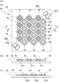
- FIG. 1A is a plan view of a light emitting device according to a first embodiment
- FIG. 1B is a cross-sectional view of the light emitting device shown in FIG. 1A taken along the line AA'
- FIG. 2 is an enlarged view of the area indicated by B in FIG. 2 is a flowchart showing a manufacturing process of the light emitting device shown in FIG.
- FIG. 4 is a diagram for explaining the first resin disposing step shown in FIG. 3
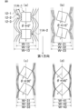
- 1A is a diagram showing the relationship between the drop amount D and the maximum width W when the angle ⁇ is 0°
- FIG. 1B is a diagram showing the relationship between the drop amount D and the maximum width W when the angle ⁇ is 15°
- FIG. 1C is a diagram showing the relationship between the drop amount D and the maximum width W when the angle ⁇ is 30°
- FIG. 1D is a diagram showing the relationship between the drop amount D and the maximum width W when the angle ⁇ is 45°.
- 1A is a diagram showing the maximum width W when the drip amount D is D1
- FIG. 1B is a diagram showing the maximum width W when the drip amount D is D2
- FIG. 1C is a diagram showing the maximum width W when the drip amount D is D3.
- 1A is a plan view of a light emitting device according to a first modified example of the first embodiment
- FIG. 1B is a cross-sectional view of the light emitting device shown in FIG. 1A along the line AA'.
- FIG. 1A is a plan view of a light emitting device according to a second modified example of the first embodiment
- FIG. 1B is a cross-sectional view of the light emitting device shown in FIG. 1A taken along the line AA'
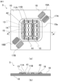
- 6A is a plan view of a light emitting device according to a second embodiment
- FIG. 6B is a cross-sectional view of the light emitting device shown in FIG. 6A taken along the line AA'
- 10A is a plan view of a light emitting device according to a third embodiment
- FIG. 10B is a cross-sectional view of the light emitting device shown in FIG. 10A taken along line AA'
- 4A is a plan view of a light emitting device according to a fourth embodiment
- FIG. 4B is a cross-sectional view of the light emitting device shown in FIG. 4A taken along line AA'.
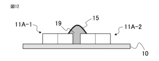
- 1 is a diagram showing a transparent resin film formed between a bonding wire and an upper surface of a substrate;
- 5A is a plan view of a light emitting device according to a fifth embodiment, and
- FIG. 5B is a cross-sectional view of the light emitting device shown in FIG. 5A taken along line AA'.
- 6A is a plan view of a light emitting device according to a sixth embodiment, and FIG. 6B is a cross-sectional view of the light emitting device shown in FIG. 6A taken along line AA'.
- 15 is a flowchart showing a manufacturing process of the light emitting device shown in FIG. 14( a ).
- FIG. 1A is a plan view of a light-emitting device according to a first modified example of the sixth embodiment
- FIG. 1B is a cross-sectional view of the light-emitting device shown in FIG. 1A along line A-A'
- FIG. 1C is a cross-sectional view of the light-emitting device shown in FIG. 1A along line B-B'.
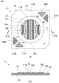
- FIG. 1(a) is a plan view of a light emitting device 1 according to a first embodiment
- FIG. 1(b) is a cross-sectional view taken along line AA' of the light emitting device 1 shown in FIG. 1(a).
- the light emitting device 1 has a substrate 10, a plurality of light emitting elements 11A and 11B mounted on the substrate 10, a first resin 12, a second resin 13, a dam material 14, and bonding wires 15.
- the plurality of light emitting elements 11A are also referred to as first light emitting elements
- the plurality of light emitting elements 11B are also referred to as second light emitting elements.
- the second resin 13 is indicated by a dashed line.
- the substrate 10 is a flat substrate made of insulating resin such as glass epoxy or ceramics.
- the substrate 10 has a square planar shape, with the first electrode pair 16A and 16B and the second electrode pair 17A and 17B disposed on the upper surface.
- the substrate 10 may be formed of a mounting substrate made of a material with high thermal conductivity such as aluminum, and an insulating circuit board on which a wiring pattern including the first electrode pair 16A and 16B and the second electrode pair 17A and 17B is formed.
- the first electrode pair 16A and 16B and the second electrode pair 17A and 17B are formed on the upper surface of the substrate 10 from a conductive material such as gold plating, and are anode and cathode terminals that supply power from an external power source (not shown) to each of the multiple light-emitting elements 11A and 11B.
- a mounting area 10a is formed that has a roughly rectangular planar shape and in which the multiple light-emitting elements 11A and 11B are mounted.
- the planar shape of the mounting area 10a is not limited to a rectangle, and may be other shapes such as an ellipse or a polygon.
- the light-emitting elements 11A and 11B are LED (Light Emitting Diode) dies that emit blue light.
- the total number of light-emitting elements 11A and 11B arranged in the mounting area 10a is 16.
- the upper surface of each of the light-emitting elements 11A and 11B has a square shape with a side length of 650 ⁇ m in a planar view, and they are mounted in the mounting area 10a of the substrate 10.
- the light-emitting colors and number of the light-emitting elements 11A and 11B are not limited to those described above, and other types of light-emitting colors and any number of elements can be used.
- the shape of the upper surface of the light-emitting elements 11A and 11B in a planar view may be a rectangular shape other than a square.
- the first resin 12 contains a phosphor, also called the first phosphor, in a transparent resin such as a silicone resin.
- the first phosphor may contain a cerium-activated garnet-based phosphor (e.g., YAG ( Y3 (Al,Ga) 5O12 : Ce3 + ) and LuAG), a europium-activated nitride-based phosphor (e.g., CASN and SCACN ((Sr,Ca) AlSiN3 :Eu2 + )), or a manganese-activated fluoride-based phosphor (e.g., KSF).
- a cerium-activated garnet-based phosphor e.g., YAG ( Y3 (Al,Ga) 5O12 : Ce3 + ) and LuAG
- a europium-activated nitride-based phosphor e.g., CASN and SCACN ((Sr,Ca
- the first phosphor mainly absorbs blue light emitted by the light-emitting element 11A and emits red, green, yellow, and other light.
- the first resin 12 is formed by being solidified by heating.
- the first resin 12 is arranged so as to cover the upper and side surfaces of the plurality of light-emitting elements 11A.
- the second resin 13 is also called a sealing material, and is a transparent resin such as a silicone resin that fills the space above the mounting area 10a inside the dam material 14, and seals the multiple light-emitting elements 11A and 11B and the first resin 12.
- the second resin 13 contains a phosphor that is also called a second phosphor, which is different from the first phosphor, and a diffusing material.
- the second phosphor is, for example, YAG, and absorbs blue light emitted from the light-emitting elements 11A and 11B and emits red, green, yellow, or other light. The color of the light emitted from the second phosphor is different from the color of the light emitted from the first phosphor.
- the second phosphor contained in the second resin 13 may be dispersed or settled within the second resin 13.
- the diffusing material diffuses the light emitted from the light-emitting elements 11A and 11B, the first phosphor, and the second phosphor.
- the second resin 13 may contain the second phosphor and not contain a diffusing material, may contain a diffusing material and not contain the second phosphor, or may not contain both the second phosphor and the diffusing material.
- the light emitting device 1 has two rows of a first light emitting element group 21 formed by four light emitting elements 11A covered with a first resin 12 and arranged adjacent to each other in a row so as to extend linearly.
- the light emitting device 1 also has two rows of a second light emitting element group 22 formed by four light emitting elements 11B not covered with the first resin 12 and arranged adjacent to the first light emitting element group 21 in a row so as to extend linearly.
- One of the two rows of the second light emitting element group 22 is formed by light emitting elements 11B mounted between the two rows of the first light emitting element group 21, and the other of the two rows of the second light emitting element group 22 is formed by light emitting elements 11B mounted between one of the two rows of the first light emitting element group 21 and the dam material 14.
- the four light emitting elements 11A are connected in series between the first electrode pairs 16A and 16B by the bonding wires 15.
- the four light emitting elements 11B are connected in series between the second electrode pairs 17A and 17B by the bonding wires 15.
- the dam material 14 is a frame material made of opaque silicone resin mixed with white particles that are a reflective material, and prevents the outflow of the second resin 13 that fills the mounting area 10a.
- the dam material 14 also reflects the light emitted from the light emitting element 11A, the light emitting element 11B, the first phosphor, and the second phosphor.
- FIG. 2 is an enlarged view of the area indicated by B in FIG. 1(a).
- FIG. 2 shows two adjacent light-emitting elements 11A and a part of the first resin 12 arranged to cover the two light-emitting elements 11A.
- one of the light-emitting elements 11A is referred to as the first adjacent light-emitting element 11A-1, and the other light-emitting element 11A is referred to as the second adjacent light-emitting element 11A-2.
- the bonding wire 15 and the first resin 12 arranged on the upper surface of the light-emitting element 11A are omitted.
- FIG. 1 shows two adjacent light-emitting elements 11A and a part of the first resin 12 arranged to cover the two light-emitting elements 11A.
- one of the light-emitting elements 11A is referred to as the first adjacent light-emitting element 11A-1
- the other light-emitting element 11A is referred to as the second adjacent light-emitting element 11A-2.
- the direction connecting the center point O1 of the upper surface of the first adjacent light-emitting element 11A-1 and the center point O2 of the upper surface of the second adjacent light-emitting element 11A-2 is referred to as the first direction
- the direction perpendicular to the first direction is referred to as the second direction.
- the first adjacent light-emitting element 11A-1 has a first side 31s, a second side 32s adjacent to the right side of the first side 31s, a third side 33s adjacent to the right side of the second side 32s, and a fourth side 34s adjacent to the right side of the third side 33s and adjacent to the left side of the first side 31s.
- the first adjacent light-emitting element 11A-1 further has a first side edge 31v, a second side edge 32v, a third side edge 33v, and a fourth side edge 34v.
- the first side edge 31v is disposed between the first side 31s and the second side 32s
- the second side edge 32v is disposed between the second side 32s and the third side 33s.
- the third side edge 33v is disposed between the third side 33s and the fourth side 34s
- the fourth side edge 34v is disposed between the fourth side 34s and the first side 31s.
- the second adjacent light-emitting element 11A-2 has a fifth side 35s, a sixth side 36s adjacent to the right side of the fifth side 35s, a seventh side 37s adjacent to the right side of the sixth side 36s, and an eighth side 38s adjacent to the right side of the seventh side 37s and adjacent to the left side of the fifth side 35s.
- the second adjacent light-emitting element 11A-2 further has a fifth side 35v, a sixth side 36v, a seventh side 37v, and an eighth side 38v.
- the fifth side 35v is disposed between the fifth side 35s and the sixth side 36s
- the sixth side 36v is disposed between the sixth side 36s and the seventh side 37s.
- the seventh side 37v is disposed between the seventh side 37s and the eighth side 38s
- the eighth side 38v is disposed between the eighth side 38s and the fifth side 35s.
- the first adjacent light-emitting element 11A-1 and the second adjacent light-emitting element 11A-2 are arranged in a plan view such that when the angle between the normal direction V1 of the first side surface 31s and the first direction is angle ⁇ , the angle between the normal direction V2 of the fifth side surface 35s and the first direction is also angle ⁇ .
- the angle ⁇ is 45°
- the distance between points O1 and O2 is, for example, 1060 ⁇ m. 1060 ⁇ m is the distance at which a light-emitting element with a side length of 650 ⁇ m can be stably mounted when the light-emitting element mounting process is performed and the light-emitting element is positioned so that the angle ⁇ is 45°.
- first adjacent light-emitting element 11A-1 and the second adjacent light-emitting element 11A-2 there is a space 30 whose sides are a first side 31s, a second side 32s, a seventh side 37s, and an eighth side 38s, as well as a virtual rectangular surface whose two opposing sides are the third side edge 32v and the sixth side edge 36v, and a virtual rectangular surface whose two opposing sides are the fourth side edge 34v and the eighth side edge 38v, and whose bottom surface is the top surface of the substrate 10.
- the first resin 12 before solidification is dripped onto the bottom surface of the space 30.
- the first resin 12 before solidification dripped onto the bottom surface of the space 30 fills the space 30 while spreading between the bottom surface of the space 30, the first side surface 31s, the second side surface 32s, the seventh side surface 37s, and the eighth side surface 38s.
- the first resin 12 before solidification filled into the space 30 gradually wets and spreads in the second direction due to the capillary phenomenon occurring between the first side surface 31s and the eighth side surface 38s, and the capillary phenomenon occurring between the second side surface 32s and the seventh side surface 37s.
- convex shapes 30a and 30b are formed outside the space 30 in a plan view, in which the first resin 12 before solidification is held by surface tension.
- the first resin 12 is solidified by heating or the like, the first resin 12 forms a first resin region 30c having convex shapes 30a and 30b.
- the first resin region 30c protrudes in the second direction at a maximum width W at a position midway between the first adjacent light emitting element 11A-1 and the second adjacent light emitting element 11A-2.
- the value of the maximum width W varies depending on the angle ⁇ and the dripping amount D.
- the dripping amount D is the amount of the first resin 12 that is dripped onto the bottom surface of the space 30 before solidification.
- the light-emitting elements 11B forming the second light-emitting element group 22 adjacent to the first light-emitting element group 21 in the second direction are positioned away from the first resin region 30c.
- the first resin 12 is less likely to come into contact with the light-emitting elements 11B, and the shape of the first resin 12 forming the first resin region 30c during manufacturing is maintained.
- the light-emitting elements 11B forming the second light-emitting element group 22 adjacent to the first light-emitting element group 21 in the second direction are positioned away in the second direction from the position of the first resin region 30c protruding at the maximum width W.
- the separation distance between the light-emitting elements 11A forming the first light-emitting element group 21 and the light-emitting elements 11B forming the second light-emitting element group 22 can be narrowed.
- the maximum width W the distance between the first light-emitting element group 21 and the second light-emitting element group 22 can be narrowed.
- FIG. 3 is a flowchart showing the manufacturing process of the light emitting device 1.
- a substrate 10 is prepared on which first electrode pairs 16A and 16B and second electrode pairs 17A and 17B are arranged (S1).
- a plurality of light-emitting elements 11A and 11B are mounted in the mounting area 10a of the substrate 10 (S2).
- the first electrode pairs 16A and 16B are connected to the plurality of light-emitting elements 11A via bonding wires 15, and the second electrode pairs 17A and 17B are connected to the plurality of light-emitting elements 11B via bonding wires 15 (S3).
- the dam material 14 is placed around the first light-emitting element group 21 and the second light-emitting element group 22 (S4).
- the first resin arrangement process an appropriate amount of the first resin 12 before solidification is dripped from a nozzle of a dripping device (not shown) so as to cover the multiple light-emitting elements 11A.
- the first resin 12 is then solidified by a predetermined heating process (S5).
- the first resin 12 contains a silicone resin, a scattering material, a YAG phosphor and a SCASN phosphor, and a thickener.
- the viscosity coefficient of the first resin 12 before solidification is 98 Pa ⁇ S.
- FIG. 4 is a diagram for explaining the first resin placement process.
- Positions 12a to 12d marked with "+" in FIG. 4 indicate the positions and order in which the first resin 12 is dropped from the nozzle of a dripping device (not shown) in the region indicated by B in FIG. 1(a) during the first resin placement process indicated by S5 in FIG. 3. Specifically, in the region indicated by B, the nozzle moves to positions 12a, 12b, 12c, and 12d in that order, and a predetermined amount of unsolidified first resin 12 is dropped at each of positions 12a, 12b, 12c, and 12d.
- the unsolidified second resin 13 is arranged inside the dam material 14 so as to seal the first light-emitting element group 21, the second light-emitting element group 22, and the first resin 12.
- the second resin 13 is then solidified by a predetermined heat treatment (S6), and the light-emitting device 1 is completed. If the second phosphor contained in the second resin 13 is allowed to settle within the second resin 13, a settling time is provided before the heat treatment. Also, if the second phosphor contained in the second resin 13 is allowed to disperse within the second resin 13, the unsolidified second resin 13 is stirred to distribute the second phosphor uniformly within the unsolidified second resin 13, and the resin is solidified by heat treatment without a settling time.
- the manufacturing process described with reference to FIG. 3 produces a light-emitting device 1 capable of emitting warm white light with a color temperature of 2200K and cool white light with a color temperature of 5000K.
- the warm white light is a first light emitted from the light-emitting element 11A included in the first light-emitting element group 21 and passing through both the first resin 12 and the second resin 13.
- the cool white light is a second light emitted from the light-emitting element 11B included in the second light-emitting element group 22 and passing through the second resin 13.
- the color temperatures of the first light and the second light are determined by adjusting the type and amount of the first phosphor and the second phosphor.
- the color temperature of the first light may be warm white light such as 2700K
- the color temperature of the second light may be cool white light such as 6500K.
- Figure 5 shows the change in maximum width W when the angle ⁇ of the light-emitting element 11A, which is the same as the light-emitting device 1, and the amount of dripping D dripped at positions 12b and 12c shown in Figure 4 are changed
- Figure 6 shows the relationship between angle ⁇ and maximum width W when the amount of dripping is changed.
- Figure 5(a) shows the relationship between drip amount D and maximum width W when the angle ⁇ is 0°
- Figure 5(b) shows the relationship between drip amount D and maximum width W when the angle ⁇ is 15°
- Figure 5(c) shows the relationship between drip amount D and maximum width W when the angle ⁇ is 30°
- Figure 5(d) shows the relationship between drip amount D and maximum width W when the angle ⁇ is 45°.
- FIG. 6(a) shows the maximum width W when the drop amount D is 0.37 mg (hereinafter referred to as D1)
- FIG. 6(b) shows the maximum width W when the drop amount D is 0.43 mg (hereinafter referred to as D2)
- FIG. 6(c) shows the maximum width W when the drop amount D is 0.61 mg (hereinafter referred to as D3).
- the region shown in FIGS. 5(a) to 5(d) corresponds to the region indicated by B in FIG. 1(a).
- the vertical axis shows the maximum width W (unit: ⁇ m)
- the horizontal axis shows the angle ⁇ (unit: °).
- the angle ⁇ between the normal direction V1 of the first side surface 31s and the first direction and the normal direction V2 of the fifth side surface 35s and the first direction of the first adjacent light-emitting element 11A-1 and the second adjacent light-emitting element 11A-2 is 0°.
- the amount of first resin 12 dispensed before solidification at positions 12b and 12c is D1
- the outline of the first resin region 30c is indicated by 12-1
- the maximum width of the first resin region 30c is indicated by W-11.
- the amount of first resin 12 dispensed before solidification at positions 12b and 12c is D2
- the outline of the first resin region 30c is indicated by 12-2
- the maximum width of the first resin region 30c is indicated by W-12.
- the amount of first resin 12 dispensed at positions 12b and 12c before solidification is D3
- the outer shape of the first resin region 30c is shown as 12-3, and the maximum width of the first resin region 30c is shown as W-13.
- the maximum width of the first resin region 30c when the dripping amount is D1 is indicated by W-21, W-31, and W-41
- the maximum width of the first resin region 30c when the dripping amount is D2 is indicated by W-22, W-32, and W-42
- the maximum width of the first resin region 30c when the dripping amount is D3 is indicated by W-23, W-33, and W-43.
- the maximum width W will be the same as when the value of the angle ⁇ is
- the maximum width W When the value of the angle ⁇ , ⁇ 1, is between 90° and 180°, the maximum width W will be the same as when the value of the angle ⁇ is (180° - ⁇ 1). Also, when ⁇ 1 is between 180° and 270°, the maximum width W will be the same as when the value of the angle ⁇ is ( ⁇ 1 - 180°). Also, when ⁇ 1 is between 270° and 360°, the maximum width W will be the same as when the value of the angle ⁇ is (360° - ⁇ 1).
- the first adjacent light-emitting element 113A-1 and the second adjacent light-emitting element 113A-2 have a square shape in a planar view, so when the value of the angle ⁇ , ⁇ 1, is 45° or more and 90° or less, the maximum width W is the same value as when the value of the angle ⁇ is (90° - ⁇ 1).
- the angle ⁇ is preferably 15° or more and 75° or less, and more preferably 30° or more and 60° or less.
- the maximum width W is smallest when the angle ⁇ is 45°, so it is more preferable that the angle ⁇ is close to 45°.
- “close” means in the range of ⁇ 10°, and more preferably in the range of ⁇ 5° (similarly, “close” to an angle below means in the range of ⁇ 10°, and more preferably in the range of ⁇ 5°).
- the shape of the light-emitting element 11A in a planar view may be rectangular.
- the shape of the light-emitting element 11A in a planar view is a rectangle with a short side length a and a long side length b ( ⁇ a)
- the angle ⁇ between the normal direction of any one of the side surfaces of each of the four light-emitting elements 11A, one of which has a short side as one side, and the first direction is arctan(b/a)
- the volume of the space 30 is maximized and the maximum width W is minimized, so it is preferable that the angle ⁇ is close to arctan(b/a).
- the ratio (b/a) of the long side length b to the short side length a is preferably 1.0 or more and 1.4 or less, and more preferably 1.0 or more and 1.1 or less.
- the angle ⁇ is 54.5°, i.e., the maximum width W is smallest in the range of about 45°
- the ratio (b/a) is 1.1
- the angle ⁇ is 47.7°, i.e., the maximum width W is smallest in the more preferable range of about 45°
- the ratio (b/a) is 1.0
- the maximum width W is smallest at the angle ⁇ of 45°.
- Fig. 7(a) is a plan view of a light emitting device 1a according to a first modified example of the first embodiment
- Fig. 7(b) is a cross-sectional view taken along line A-A' of the light emitting device shown in Fig. 7(a).
- components similar to those in the light emitting device 1 are designated by the same reference numerals and will not be described.
- the light emitting device 1a shown in FIG. 7 differs from the light emitting device 1 only in that the orientation of the four light emitting elements 11B in the second light emitting element group 22a is different.
- the four light emitting elements 11B are mounted in a row on the substrate 10 along the first direction, and the angle that the normal direction of any one of the four side surfaces of each of the four light emitting elements 11B makes with the first direction is 0°.
- the angle that the normal direction of any one of the four side surfaces of each of the four light-emitting elements 11B makes with the first direction is 0°, but it is sufficient that the angle that the normal direction of any one of the four side surfaces of each of the four light-emitting elements 11A makes with the first direction is less than the angle ⁇ .
- the angle that the normal direction of any one of the four side surfaces of each of the four light-emitting elements 11B makes with the first direction smaller than the angle ⁇ , the distance between the first light-emitting element group 21 and the second light-emitting element group 22a can be further narrowed.
- the angle that the normal direction of any one of the four side surfaces of each of the four light-emitting elements 11B makes with the first direction is close to 0°.
- the shape of the light-emitting element 11B in a planar view may be rectangular.
- the shape of the light-emitting element 11B in a planar view is a rectangle having short and long sides, it is more preferable that the angle between the normal direction of any one of the side faces of each of the four light-emitting elements 11B, which has the short side as one side, and the first direction is close to 0°.
- Fig. 8(a) is a plan view of a light emitting device 1b according to a second modified example of the first embodiment
- Fig. 8(b) is a cross-sectional view taken along line A-A' of the light emitting device shown in Fig. 8(a).
- components similar to those of the light emitting device 1 are designated by the same reference numerals and will not be described.
- Light emitting device 1b differs from light emitting device 1 only in that it has a third resin 23 that covers the second light emitting element group 22 and contains a third phosphor.
- the second resin 13 seals the first resin 12 and the third resin 23.
- the third resin 23 is a transparent resin such as silicone resin that contains a phosphor also called the third phosphor, and mainly absorbs the blue light emitted by the light emitting element 11B and emits red, green, yellow, and other light.
- the color of the light emitted from the third phosphor is different from the colors of the light emitted from the first phosphor and the second phosphor.
- the third phosphor includes cerium-activated garnet phosphors including YAG and LuAG, europium-activated nitride phosphors including CASN and SCACN, or manganese-activated fluoride phosphors including KSF.
- the third resin 23 is solidified by heating.
- the freedom to select the light emitted from the light emitting device 1b is increased. Furthermore, by setting the angle between the normal direction of any one of the four side surfaces of each of the light emitting elements 11B and the first direction to 15° or more and 75° or less, the maximum width of the third resin 23 can be controlled, and the second light emitting element group 22 can be arranged closer to the first light emitting element group 21.
- the angle between the normal direction of any one of the four side surfaces of each of the light emitting elements 11B and the first direction is set to 30° or more and 60° or less, the maximum width of the third resin 23 can be controlled, and the second light emitting element group 22 can be arranged even closer to the first light emitting element group 21.
- the shape of the light emitting element 11B is a square in a plan view, it is even more preferable that the angle between the normal direction of any one of the four side surfaces of each of the light emitting elements 11B and the first direction is approximately 45°.
- the shape of the light-emitting element 11B in a plan view is a rectangle with a short side length a and a long side length b ( ⁇ a)
- it is preferable that the angle that the normal direction of any one of the side surfaces having the short sides of the light-emitting element 11B makes with the first direction is close to arctan(b/a).
- the ratio (b/a) of the long side length b to the short side length a is preferably 1.0 or more and 1.4 or less, and more preferably 1.0 or more and 1.1 or less.
- the angle ⁇ is 54.5°, i.e., the maximum width W is smallest in the range of about 45°
- the ratio (b/a) is 1.1
- the angle ⁇ is 47.7°, i.e., the maximum width W is smallest in the more preferable range of about 45°
- the ratio (b/a) is 1.0
- the maximum width W is smallest at the angle ⁇ of 45°.
- Fig. 9(a) is a plan view of a light emitting device 2 according to a second embodiment
- Fig. 9(b) is a cross-sectional view taken along line A-A' of the light emitting device shown in Fig. 9(a).
- the same components as those in the light emitting device 1 are denoted by the same reference numerals and will not be described.
- Light emitting device 2 differs from light emitting device 1 in the arrangement of the first resin 12.
- the first resin 12 is arranged to cover the side and top surface of light emitting element 11A that face the side surface of adjacent light emitting element A, but is not arranged to cover the side surface of light emitting element 11A that faces dam material 14.
- the first resin 12 is arranged to cover all side surfaces and top surface of light emitting element 11A, including the side surface that faces dam material 14.
- the manufacturing method of the light emitting device 2 differs from the manufacturing method of the light emitting device 1 in that in the first resin disposing step shown as S5 in FIG. 3, the first resin 12 before solidification is dripped between the dam material 14 and the end of the first light emitting element group 21.
- the substrate preparation step, the light emitting element mounting step, the wire bonding step, the dam material disposing step, and the second resin disposing step are the same as in the manufacturing method of the light emitting device 1, so their explanations are omitted.
- the first resin 12 arranged on the upper surface of the light emitting element 11A adjacent to the dam material 14 is solidified in a state where it is arranged so as to protrude from the upper surface toward the dam material 14, and there is a risk of a protrusion being formed that protrudes from the upper surface of the light emitting element 11A toward the dam material 14.
- the second phosphor is allowed to settle, when a protrusion is formed in the first resin 12 protruding from the upper surface of the light emitting element 11A toward the dam material 14, the second phosphor contained in the second resin 13 settles on the upper surface of the protrusion and does not settle between the upper surface of the substrate 10 and the lower surface of the protrusion.
- the amount of light that is absorbed by the second phosphor from the side of the light emitting element 11A on which the protrusion is formed toward the dam material 14 differs from the amount of light that is absorbed by the second phosphor from the side of the light emitting element 11A on which the protrusion is not formed and is received by the dam material 14 and emitted.
- the amount of light emitted from the side of the light emitting element 11A on which a protrusion is formed toward the dam material 14 and absorbed by the second phosphor differs from the amount of light emitted from the side of the light emitting element 11A on which a protrusion is formed and absorbed by the second phosphor, so there is a risk of color unevenness occurring near the dam material 14.
- the first resin 12 is arranged to cover all side surfaces of the light emitting element 11A, including the side surface facing the dam material 14, so no protrusion is formed protruding from the top surface of the light emitting element 11A toward the dam material 14, and there is a low risk of color unevenness occurring near the dam material 14.
- a first resin 12 is disposed between the dam material 14 and the first light emitting element group 21 of the light emitting device 1.
- the first resin 12 may be disposed between the first light emitting element group formed by the light emitting elements 11A and the dam material, as in the light emitting device 2.
- a third resin 23 may be disposed between the second light emitting element group 22 formed by the light emitting elements 11B and the dam material 14.
- Fig. 10(a) is a plan view of a light-emitting device 3 according to a third embodiment
- Fig. 10(b) is a cross-sectional view taken along line A-A' of the light-emitting device shown in Fig. 10(a).
- the same components as those in the light-emitting device 1 are denoted by the same reference numerals, and the description thereof will be omitted.
- the shapes of the dam material 14a, the mounting area 10b, the first electrode pair 26A and 26B, and the second electrode pair 27A and 27B are different from the shapes of the dam material 14, the mounting area 10a, the first electrode pair 16A and 16B, and the second electrode pair 17A and 17B.
- the mounting area 10b is a circular area inside the dam material 14a having a circular planar shape.
- the arrangement of the first resin 12 is different from that of the light emitting device 1.
- the number of light emitting elements 11A forming the first light emitting element group 21a is eight, and the number of light emitting elements 11A forming the other first light emitting element group 21b is four.
- the light emitting elements 11A are arranged such that the angle ⁇ between the normal direction of any one of the four side surfaces and the first direction is 45°, and are covered with the first resin 12.
- a first resin 12 is disposed between the dam material 14a and the first light-emitting element groups 21a and 21b.
- a second light-emitting element group 22c that is not covered with the first resin 12 and is formed by the light-emitting elements 11B is disposed between the first light-emitting element groups 21a and 21b.
- the light-emitting elements 11B are disposed such that the angle between the normal direction of any one of the four side surfaces and the first direction is 0°.
- the number of light-emitting elements 11A that form the first light-emitting element group 21a and the number of light-emitting elements 11A that form the pair of first light-emitting element groups 21b that are connected in series are the same, eight, and each is connected in series between the first electrode pairs 26A and 26B.
- the eight light-emitting elements 11B that form the second light-emitting element group 22c are connected in series between the second electrode pairs 27A and 27B.
- Each of the pair of first light-emitting element groups 21b is arranged separately outside the first light-emitting element group 21a and the second light-emitting element group 22c, and is formed by four light-emitting elements 11A.
- the light-emitting elements 11A forming each of the pair of first light-emitting element groups 21b are connected in series below the dam 14a. Since each of the pair of first light-emitting element groups 21b is arranged separately outside the first light-emitting element group 21a and the second light-emitting element group 22c, the light-emitting elements 11A and 11B can be evenly arranged in the circular mounting area 10b.
- At least one of the light-emitting elements 11A forming the first light-emitting element groups 21a and 21b and the light-emitting elements 11B forming the second light-emitting element group 22c may be shifted outward.
- the light-emitting elements 11A forming the first light-emitting element groups 21a and 21b and the light-emitting elements 11B forming the second light-emitting element group 22c are shifted outward, the light-emitting elements 11A and 11B can be evenly arranged in the circular mounting area 10b.
- the light-emitting elements 11A forming the first light-emitting element groups 21a and 21b are arranged such that the angle ⁇ between the normal direction of any one of the four side surfaces and the first direction is 15° or more and 75° or less, so that the spacing between the adjacent second light-emitting element groups can be narrowed.
- Fig. 11(a) is a plan view of a light-emitting device 4 according to a fourth embodiment
- Fig. 11(b) is a cross-sectional view taken along line A-A' of the light-emitting device shown in Fig. 11(a).
- the same components as those in the light-emitting device 1 are denoted by the same reference numerals and will not be described.
- Light emitting device 4 differs from light emitting device 1 in that it has reflective resin 40. Similar to dam material 14, reflective resin 40 is made of opaque silicone resin mixed with white particles that act as a reflective material, and is disposed between dam material 14 and first light emitting element group 21 and second light emitting element group 22.
- the manufacturing method of the light emitting device 4 differs from the manufacturing method of the light emitting device 1 in that it has a reflective resin disposing step between the first resin disposing step shown as S5 in FIG. 3 and the second resin disposing step shown as S6 in FIG. 3.
- the substrate preparation step, the light emitting element mounting step, the wire bonding step, the dam material disposing step, the first resin disposing step, and the second resin disposing step are the same as in the manufacturing method of the light emitting device 1, so the description will be omitted.
- reflective resin 40 before solidification is dripped from a nozzle of a dripping device (not shown) near the side surfaces of the light emitting elements 11A and 11B arranged at the ends in the first direction of the first light emitting element group 21 and the second light emitting element group 22 that face the dam material 14, and spreads out while being held by the tension of the side surfaces.
- the viscosity coefficient of the reflective resin 40 before solidification is approximately the same as the viscosity coefficient of the first resin 12 before solidification, and it is solidified by a specified heat treatment.
- the light emitting device 4 has a reflective resin 40 disposed between the dam material 14 and the first and second light emitting element groups 21 and 22, so that regardless of the distance between the dam material 14 and the ends of the first and second light emitting element groups 21 and 22, a yellow ring caused by the second phosphor contained in the second resin 13 does not occur.
- a reflective resin 40 is disposed between the dam material 14 of the light emitting device 1 and the first and second light emitting element groups 21 and 22.
- a reflective resin 40 may be disposed between the dam material and the first and second light emitting element groups formed by the light emitting elements 11A and 11B.
- the light emitting device In the above-mentioned light emitting device, synthetic resins such as the first resin 12 and the second resin 13 are directly disposed on the substrate 10, the light emitting elements 11A and 11B, and the bonding wire 15.
- the light emitting device according to the embodiment may have a transparent resin disposed between the substrate 10, the light emitting elements 11A and 11B, and the bonding wire 15 and the synthetic resins such as the first resin 12 and the second resin 13.
- the transparent resin is a film made of a transparent synthetic resin containing an acrylic resin, a silicone resin, and a fluoride compound.
- a transparent resin disposing step is carried out between the dam material disposing step shown at S4 in FIG. 3 and the first resin disposing step shown at S5.
- the transparent resin before solidification is applied over the entire surfaces of the substrate 10, the light emitting elements 11A and 11B, and the bonding wires 15, and then the substrate 10 is heat-treated to dispose the transparent resin.
- the light emitting device may also have a transparent resin film formed between the bonding wire 15 and the upper surface of the substrate 10.
- the transparent resin film is made of the same resin as the transparent resin disposed between the substrate 10, the light emitting elements 11A and 11B, and the bonding wire 15 and synthetic resins such as the first resin 12 and the second resin.
- FIG. 12 is a diagram showing a transparent resin film formed between the bonding wire 15 and the upper surface of the substrate 10.
- FIG. 12 is a diagram corresponding to a side view of the area indicated by B in FIG. 1(a).
- components other than the substrate 10, the first adjacent light-emitting element 11A-1 and the second adjacent light-emitting element 11A-2, the bonding wire 15, and the transparent resin are omitted.
- the transparent resin film 19 is formed over the entire surface between the bonding wires 15 that connect the light-emitting elements 11A and the bonding wires 15 that connect the light-emitting elements 11B and the substrate 10.
- the light emitting device has a transparent resin film 19 formed between the bonding wire 15 and the upper surface of the substrate 10, so that when the unsolidified first resin 12 is dripped, the unsolidified first resin 12 tends to accumulate near the bonding wire 15.
- the light emitting device according to the embodiment can further reduce the maximum width W of the first resin region 30c by making it easier for the unsolidified first resin 12 to accumulate near the bonding wire 15.
- the transparent resin film 19 may be formed at least partially between the bonding wires 15 that connect the light emitting elements 11A and the bonding wires 15 that connect the light emitting elements 11B and the substrate 10.
- the transparent resin film 19 may not be formed over the entire surface between the bonding wires 15 and the substrate 10, but an opening may be formed. Even if an opening is formed in the transparent resin film 19 formed between the bonding wires 15 and the substrate 10, the maximum width W of the first resin region 30c can be reduced by forming the transparent resin film 19.
- Fig. 13(a) is a plan view of a light-emitting device 5 according to the fifth embodiment
- Fig. 13(b) is a cross-sectional view taken along line A-A' of the light-emitting device shown in Fig. 13(a).
- the same components as those in the light-emitting device 1 are denoted by the same reference numerals, and the description thereof will be omitted.
- Light emitting device 5 differs from light emitting device 1 in that it has a first fluorescent resin 41. It also differs from light emitting device 1 in that it has a first resin 42 instead of first resin 12. Like first resin 12, first fluorescent resin 41 contains a phosphor also referred to as a first phosphor. The type of phosphor contained in first fluorescent resin 41 is the same as the phosphor contained in first resin 12.
- the first fluorescent resin 41 is arranged so as to cover at least a portion of the side surfaces and the top surfaces of the multiple light-emitting elements 11A.
- the first fluorescent resin 41 is arranged so as to cover the top surfaces of all the light-emitting elements 11A, and is arranged so as to cover the side surfaces of the light-emitting elements 11A that do not face the dam material 14.
- the first fluorescent resin 41 is not arranged on the side surfaces of the light-emitting elements 11A that face the dam material 14.
- the first resin 42 is formed of an opaque silicone resin mixed with white particles, which are a reflective material, in the same manner as the dam material 14, and is arranged to cover the side of the light-emitting element 11A facing the dam material 14, and is a resin that reflects the light emitted from the light-emitting elements 11A and 11B.
- the first resin 42 is arranged between a pair of side surfaces of the two light-emitting elements 11A arranged to be spaced apart as they approach the dam material 14, in the same manner as the first resin 12.
- the first resin 42 is also arranged between a pair of side surfaces of the two light-emitting elements 11B arranged to be spaced apart as they approach the dam material 14, in the same manner as the first resin 12.
- the first resin 42 is further arranged between the end in the first direction shown in FIG. 2 of each of the multiple first light-emitting element groups formed by the light-emitting elements 11A and the multiple second light-emitting element groups formed by the light-emitting elements 11B and the dam material 14.
- the manufacturing method of the light emitting device 5 differs from the manufacturing method of the light emitting device 1 in that it has a first phosphor resin disposing step instead of the first resin disposing step shown in S5 in FIG. 3.
- a transparent resin film disposing step is performed between the dam material disposing step shown in S4 in FIG. 3 and the first resin disposing step shown in S5 in FIG. 3.
- the transparent resin film disposing step the transparent resin before solidification is applied over the entire surfaces of the substrate 10, the light emitting elements 11A and 11B, and the bonding wire 15, and then the substrate 10 is heat-treated, and a transparent resin film is disposed between the bonding wire 15 and the upper surface of the substrate 10.
- the manufacturing method of the light emitting device 5 differs from the manufacturing method of the light emitting device 1 in that it has a first resin disposing step between the first resin disposing step shown in S5 in FIG. 3 and the second resin disposing step shown in S6 in FIG. 3.
- the substrate preparation step, the light emitting element mounting step, the wire bonding step, the dam material disposing step, and the second resin disposing step are the same as in the manufacturing method of the light emitting device 1, so their explanations are omitted.
- the first fluorescent resin placement step is the same as the first resin placement step shown in S5 in FIG. 3, except that the first fluorescent resin 41 before solidification is not dripped at position 12b shown in FIG. 4, but rather the first fluorescent resin 41 before solidification is dripped at positions 12a, 12c, and 12d in that order.
- the first resin 42 before solidification is dripped from a nozzle of a dripping device (not shown) near the side of the light emitting elements 11A and 11B that faces the dam material 14.
- the first resin 42 is dripped between the pair of side surfaces of the two light emitting elements 11A and 11B that are arranged so as to move apart as it approaches the dam material 14, and spreads out while being held by the tension between the pair of sides.
- the viscosity coefficient of the first resin 42 before solidification is approximately the same as the viscosity coefficient of the first resin 12 before solidification, and it is solidified by a specified heat treatment.
- the light emitting device 5 has a reflective first resin 42 disposed between the light emitting elements 11A and 11B and the dam material 14, so there is no risk of the light emitted from the light emitting elements 11A and 11B becoming stray light between the light emitting elements 11A and 11B and the dam material 14.
- the light emitting device 5 has no risk of the light emitting efficiency decreasing due to stray light, so there is no risk of the light emitted from the light emitting elements 11A and 11B becoming stray light between the light emitting elements 11A and 11B and the dam material 14.
- the angle between the extension direction of the bonding wire 15 connecting two adjacent light emitting elements 11A to each other in a planar view and the first direction is preferably smaller than the angle ⁇ , and more preferably close to 0°.
- the angle between the extension direction of the bonding wire 15 in a planar view and the first direction is smaller than the angle ⁇ , the first resin 12 before solidification can be stably dripped in the first resin arrangement step, thereby suppressing the variation in the maximum width W.
- the light emitting device according to the embodiment can narrow the spacing between multiple light emitting element groups by suppressing the variation in the maximum width W.
- the bonding wire 15 connecting two adjacent light emitting elements 11A to each other is preferably arranged so as to be point symmetric about the midpoint between the centers of the two light emitting elements 11A connected by the bonding wire 15.
- the bonding wire 15 By arranging the bonding wire 15 so as to be point symmetric about the midpoint between the centers of the two light emitting elements 11A being connected, the first resin 12 before solidification can be stably dripped in the first resin arrangement step, thereby suppressing the variation in the maximum width W.
- the light emitting device according to the embodiment can narrow the spacing between multiple light emitting element groups by suppressing the variation in the maximum width W.
- the bonding wire 15 connecting two adjacent light emitting elements 11A to each other is arranged so as to be linearly symmetrical about the center line connecting the centers of the two light emitting elements 11A connected by the bonding wire 15.
- the bonding wire 15 is arranged so as to coincide with the center line connecting the centers of the light emitting elements 11A, so as to be linearly symmetrical about the center line connecting the centers of the light emitting elements 11A connected by the bonding wire 15.
- the bonding wire 15 is arranged so as to be linearly symmetrical about the center line connecting the centers of the light emitting elements 11A, so that the first resin 12 before solidification can be stably dripped in the first resin arrangement step, and the variation in the maximum width W can be suppressed.
- the variation in the maximum width W can be suppressed, so that the interval between the multiple light emitting element groups can be narrowed.
- the first resin is formed by dripping the first resin before solidification at positions 12a, 12b, 12c, and 12d.
- the resin dripped at positions 12a and 12d may be different from the resin dripped at positions 12b and 12c.
- the resin dripped at positions 12a and 12d may contain a phosphor, and the resin dripped at positions 12b and 12c may contain a reflective material.
- the first resin is formed by dripping the first resin before solidification at positions 12a, 12b, 12c, and 12d.
- the first resin may be formed by continuously applying the first resin before solidification in the first direction along the light-emitting elements 11A that form the first light-emitting element group.
- the viscosity coefficient of the first resin before solidification is 50 Pa ⁇ S or more and 150 Pa ⁇ S or less.
- the amount of the first resin before solidification filled into the space 30 is 0.4 mg or more and 0.6 mg or less.
- the dam material 14 is disposed around the light emitting elements 11A and 11B, but in the light emitting device according to the embodiment, the dam material 14 may be omitted.
- the first resin is held in place by the capillary phenomenon that occurs between the side surfaces of the light emitting elements.
- FIG. 14(a) is a plan view of a light emitting device 6 according to the sixth embodiment
- FIG. 14(b) is a cross-sectional view taken along line AA' of the light emitting device shown in FIG. 14(a).
- the light emitting device 6 has a substrate 50, a plurality of light emitting elements 51A and 51B mounted on the substrate 50, a first resin 52, a first fluorescent sheet 53, and a second fluorescent sheet 54.
- the substrate 50 has a similar configuration to the substrate 10, and a first electrode pair 56A and 56B and a second electrode pair 57A and 57B are disposed on the upper surface.
- the first electrode pair 56A and 56B and the second electrode pair 57A and 57B are formed on the upper surface of the substrate 50 from a conductive material such as gold plating, and are anode and cathode terminals that supply power from an external power source (not shown) to each of the multiple light-emitting elements 51A and 51B.
- the light-emitting elements 51A and 51B are LED dies that emit blue light.
- the total number of light-emitting elements 51A and 51B mounted on the substrate 50 is 16.
- the upper surface of each of the light-emitting elements 51A and 51B has a square shape in a plan view, and they are mounted by being connected face-down to the substrate 50.
- the light-emitting colors and number of the light-emitting elements 51A and 51B are not limited to those described above, and other types of light-emitting colors and any number of elements can be used.
- the shape of the upper surface of the light-emitting elements 51A and 51B in a plan view may be a rectangular shape other than a square.
- the light-emitting elements 51A and 51B are arranged in four rows and four columns so as to form a roughly square shape when viewed in a plane.
- the light-emitting elements 51A and 51B are mounted so that four light-emitting elements 51A are arranged in the first column 61 and the third column 63, and four light-emitting elements 51B are arranged in the second column 62 and the fourth column 64.
- the light-emitting elements 51A and 51B are mounted so as to be arranged alternately in each of the first row 65 to the fourth row 68.
- each of the light-emitting elements 51A and 51B is arranged so that its side surface is inclined at 45° with respect to the row direction and column direction in which the light-emitting elements 51A and 51B are arranged.
- the four light-emitting elements 51A arranged in the first column 61 and the third column 63 are connected in series between the first electrode pairs 56A and 56B, and the four light-emitting elements 51B arranged in the second column 62 and the fourth column 64 are connected in series between the second electrode pairs 57A and 57B.
- the first resin 52 is made of an opaque silicone resin mixed with white particles that act as a reflective material.
- the first resin 52 functions as a sealant that seals the light-emitting elements 51A and 51B, and also functions as a reflective material that reflects the light emitted from the light-emitting elements 51A and 51B.
- the outer edge of the first resin 52 is formed by the first resin before solidification being held by the capillary phenomenon that occurs between the side surfaces of the light-emitting elements.
- the first fluorescent sheet 53 has a rectangular planar shape and is a sheet material containing a phosphor.
- the first fluorescent sheet 53 is arranged so as to cover the upper surface of the light-emitting element 11A.
- the type of phosphor contained in the first fluorescent sheet 53 is the same as the phosphor contained in the first resin 12.
- the first fluorescent sheet 53 is arranged so that its side surfaces are parallel to the side surfaces of the light-emitting elements 51A, and when viewed in a plan view, the side surfaces are arranged at an angle of 45° to the row and column directions in which the light-emitting elements 51A are arranged.
- the second fluorescent sheet 54 has a rectangular planar shape and is a sheet material containing a phosphor.
- the second fluorescent sheet 54 is arranged so as to cover the upper surface of the light-emitting element 11B.
- the second fluorescent sheet 54 contains the second phosphor, similar to the second resin 13.
- the second fluorescent sheet 54 is arranged so that its side surfaces are parallel to the side surfaces of the light-emitting elements 51B, and when viewed in a plan view, the side surfaces are arranged at an angle of 45° to the row and column directions in which the light-emitting elements 51B are arranged.
- FIG. 15 is a flowchart showing a method for manufacturing the light-emitting device 6.
- a substrate 50 is prepared on which a first electrode pair 56A and 56B and a second electrode pair 57A and 57B are arranged (S11).
- a plurality of light-emitting elements 51A and 51B are mounted on the upper surface of substrate 50 of substrate 10 by face-down connection (S12).
- the first fluorescent sheet 53 is arranged by being adhered to the upper surface of the light emitting element 51A via a transparent adhesive (S13).
- the adhesive that adheres the first fluorescent sheet 53 to the upper surface of the light emitting element 51A is solidified to form a transparent resin that covers the side surface of the light emitting element 51A.
- the second fluorescent sheet 54 is arranged by being adhered to the upper surface of the light emitting element 51B via a transparent adhesive (S14).
- the adhesive that adheres the second fluorescent sheet 54 to the upper surface of the light emitting element 51B is solidified to form a transparent resin that covers the side surface of the light emitting element 51B.
- the first resin arrangement step an appropriate amount of unsolidified first resin 52 is dripped from a nozzle of a dripping device (not shown) so as to cover the multiple light emitting elements 11A and 11B, and then solidified to form the light emitting device 5 (S15).
- the first resin 52 contains a silicone resin, a reflective material, and a thickener.
- the viscosity coefficient of the first resin 52 before solidification is approximately the same as the viscosity coefficient of the first resin 12 before solidification, and it is solidified by a specified heat treatment.
- Fig. 16(a) is a plan view of a light emitting device 6a according to a first modified example of the sixth embodiment
- Fig. 16(b) is a cross-sectional view taken along line A-A' of the light emitting device shown in Fig. 16(a)
- Fig. 16(c) is a cross-sectional view taken along line B-B' of the light emitting device shown in Fig. 16(a).
- components similar to those in the light emitting device 6 are given the same numbers and will not be described.
- the light-emitting device 6a differs from the light-emitting device 6 in the number of light-emitting elements 51A and 51B arranged and in the arrangement of the light-emitting elements 51A and 51B.
- the total number of light-emitting elements 51A and 51B mounted on the substrate 50 is 24, which is 1.5 times the total number of light-emitting elements 51A and 51B mounted on the substrate 50 in the light-emitting device 6.
- the light-emitting elements 51A and 51B are mounted such that four light-emitting elements 51A are arranged in the first column 71, the third column 73, and the fifth column 75, and four light-emitting elements 51B are arranged in the second row 72, the fourth column 74, and the sixth row 76.
- each of the light-emitting elements 51A and 51B is arranged with its side surface inclined at 45° with respect to the row direction and column direction in which the light-emitting elements 51A and 51B are arranged.
- the four light-emitting elements 51A arranged in the first column 71, the third column 73, and the fifth column 75 are connected in series between the first electrode pairs 56A and 56B, and the four light-emitting elements 51B arranged in the second column 72, the fourth column 74, and the sixth column 76 are connected in series between the second electrode pairs 57A and 57B.
- the first row 81 of the light-emitting elements 51A is arranged so as to be positioned outside the first row 82 of the light-emitting elements 51B.
- the first row 82 of the light-emitting elements 51B is arranged between the first row 81 of the light-emitting elements 51A and the second row 83 of the light-emitting elements 51A.
- the second row 83 of the light-emitting elements 51A is arranged between the first row 82 of the light-emitting elements 51B and the second row 84 of the light-emitting elements 51B.
- the second row 84 of the light-emitting elements 51B is arranged between the second row 83 of the light-emitting elements 51A and the third row 85 of the light-emitting elements 51A.
- the third row 85 of the light-emitting elements 51A is arranged between the second row 84 of the light-emitting elements 51B and the third row 86 of the light-emitting elements 51B.
- the third row 86 of the light-emitting elements 51B is arranged between the third row 85 of the light-emitting elements 51A and the fourth row 87 of the light-emitting elements 51A.
- the fourth row 87 of the light-emitting elements 51A is arranged between the third row 86 of the light-emitting elements 51B and the fourth row 88 of the light-emitting elements 51B.
- the fourth row 88 of the light-emitting elements 51B is positioned outside the fourth row 87 of the light-emitting elements 51A.
- the light-emitting device 6a can mount the light-emitting elements 51A and 51B at a higher density than the light-emitting device 6 by shifting the row-direction arrangement of the light-emitting elements 51A from the row-direction arrangement of the light-emitting elements 51B.
Landscapes
- Led Device Packages (AREA)
Priority Applications (2)
| Application Number | Priority Date | Filing Date | Title |
|---|---|---|---|
| JP2024541751A JP7562052B1 (ja) | 2023-03-23 | 2024-02-20 | 発光装置 |
| CN202480003812.3A CN120858665A (zh) | 2023-03-23 | 2024-02-20 | 发光装置 |
Applications Claiming Priority (2)
| Application Number | Priority Date | Filing Date | Title |
|---|---|---|---|
| JP2023047180 | 2023-03-23 | ||
| JP2023-047180 | 2023-03-23 |
Publications (1)
| Publication Number | Publication Date |
|---|---|
| WO2024195399A1 true WO2024195399A1 (ja) | 2024-09-26 |
Family
ID=92841368
Family Applications (1)
| Application Number | Title | Priority Date | Filing Date |
|---|---|---|---|
| PCT/JP2024/005974 Ceased WO2024195399A1 (ja) | 2023-03-23 | 2024-02-20 | 発光装置 |
Country Status (3)
| Country | Link |
|---|---|
| JP (1) | JP7562052B1 (https=) |
| CN (1) | CN120858665A (https=) |
| WO (1) | WO2024195399A1 (https=) |
Citations (10)
| Publication number | Priority date | Publication date | Assignee | Title |
|---|---|---|---|---|
| US6666567B1 (en) * | 1999-12-28 | 2003-12-23 | Honeywell International Inc. | Methods and apparatus for a light source with a raised LED structure |
| JP2012054383A (ja) * | 2010-09-01 | 2012-03-15 | Citizen Holdings Co Ltd | 半導体発光装置及びその製造方法 |
| US20150034978A1 (en) * | 2013-08-01 | 2015-02-05 | Cree, Inc. | Light emitter devices and methods for light emitting diode (led) chips |
| JP2017050445A (ja) * | 2015-09-03 | 2017-03-09 | パナソニックIpマネジメント株式会社 | 発光装置、及び照明装置 |
| JP2017085096A (ja) * | 2015-10-23 | 2017-05-18 | シチズン電子株式会社 | 発光モジュール |
| JP2018022884A (ja) * | 2016-07-21 | 2018-02-08 | シチズン電子株式会社 | 発光装置 |
| JP2019016780A (ja) * | 2017-07-04 | 2019-01-31 | 日亜化学工業株式会社 | 発光装置 |
| JP2019096741A (ja) * | 2017-11-22 | 2019-06-20 | シチズン電子株式会社 | 発光装置 |
| JP2019121790A (ja) * | 2017-12-27 | 2019-07-22 | 日亜化学工業株式会社 | 発光装置 |
| JP2020205327A (ja) * | 2019-06-17 | 2020-12-24 | シチズン電子株式会社 | 発光装置 |
Family Cites Families (8)
| Publication number | Priority date | Publication date | Assignee | Title |
|---|---|---|---|---|
| EP2717338B1 (en) * | 2011-05-27 | 2018-08-01 | Sharp Kabushiki Kaisha | Light emitting device and lighting device |
| JP6095479B2 (ja) * | 2013-05-17 | 2017-03-15 | シチズン時計株式会社 | Ledモジュール |
| JP6705476B2 (ja) * | 2017-09-29 | 2020-06-03 | 日亜化学工業株式会社 | 発光装置 |
| JP2020030905A (ja) * | 2018-08-21 | 2020-02-27 | シチズン時計株式会社 | Led発光装置 |
| JP7332979B2 (ja) * | 2019-01-23 | 2023-08-24 | 東芝ライテック株式会社 | 発光モジュール、および照明装置 |
| JP2020136619A (ja) * | 2019-02-25 | 2020-08-31 | パナソニックIpマネジメント株式会社 | 発光装置及び照明装置 |
| JP7410734B2 (ja) * | 2020-02-05 | 2024-01-10 | シチズン時計株式会社 | Led発光装置 |
| JP7180032B2 (ja) * | 2020-03-10 | 2022-11-29 | シチズン電子株式会社 | 発光装置 |
-
2024
- 2024-02-20 CN CN202480003812.3A patent/CN120858665A/zh active Pending
- 2024-02-20 WO PCT/JP2024/005974 patent/WO2024195399A1/ja not_active Ceased
- 2024-02-20 JP JP2024541751A patent/JP7562052B1/ja active Active
Patent Citations (10)
| Publication number | Priority date | Publication date | Assignee | Title |
|---|---|---|---|---|
| US6666567B1 (en) * | 1999-12-28 | 2003-12-23 | Honeywell International Inc. | Methods and apparatus for a light source with a raised LED structure |
| JP2012054383A (ja) * | 2010-09-01 | 2012-03-15 | Citizen Holdings Co Ltd | 半導体発光装置及びその製造方法 |
| US20150034978A1 (en) * | 2013-08-01 | 2015-02-05 | Cree, Inc. | Light emitter devices and methods for light emitting diode (led) chips |
| JP2017050445A (ja) * | 2015-09-03 | 2017-03-09 | パナソニックIpマネジメント株式会社 | 発光装置、及び照明装置 |
| JP2017085096A (ja) * | 2015-10-23 | 2017-05-18 | シチズン電子株式会社 | 発光モジュール |
| JP2018022884A (ja) * | 2016-07-21 | 2018-02-08 | シチズン電子株式会社 | 発光装置 |
| JP2019016780A (ja) * | 2017-07-04 | 2019-01-31 | 日亜化学工業株式会社 | 発光装置 |
| JP2019096741A (ja) * | 2017-11-22 | 2019-06-20 | シチズン電子株式会社 | 発光装置 |
| JP2019121790A (ja) * | 2017-12-27 | 2019-07-22 | 日亜化学工業株式会社 | 発光装置 |
| JP2020205327A (ja) * | 2019-06-17 | 2020-12-24 | シチズン電子株式会社 | 発光装置 |
Also Published As
| Publication number | Publication date |
|---|---|
| JP7562052B1 (ja) | 2024-10-04 |
| JPWO2024195399A1 (https=) | 2024-09-26 |
| CN120858665A (zh) | 2025-10-28 |
Similar Documents
| Publication | Publication Date | Title |
|---|---|---|
| JP5089212B2 (ja) | 発光装置およびそれを用いたledランプ、発光装置の製造方法 | |
| JP5753446B2 (ja) | 半導体発光装置の製造方法 | |
| JP7179923B2 (ja) | 発光装置および調色装置 | |
| US20130105835A1 (en) | Light-emitting diode device | |
| US20170196060A1 (en) | Light-emitting apparatus and color-matching apparatus | |
| KR102797888B1 (ko) | 발광 장치 | |
| WO2013015058A1 (ja) | 発光装置 | |
| JP2008235824A5 (https=) | ||
| JP6107060B2 (ja) | 発光装置の製造方法 | |
| JP2019016780A (ja) | 発光装置 | |
| JP7372526B2 (ja) | 発光装置の製造方法及び発光モジュールの製造方法 | |
| US11855242B2 (en) | Light emitting device and method of manufacturing the same | |
| JP2016174120A (ja) | 発光装置 | |
| JP6566791B2 (ja) | 発光装置 | |
| JP2018073950A (ja) | 発光モジュール及び照明器具 | |
| JP7562052B1 (ja) | 発光装置 | |
| JP7111993B2 (ja) | 発光モジュールの製造方法 | |
| US10161574B2 (en) | Light-emitting device, lighting device, and method of manufacturing light-emitting device | |
| US11798920B2 (en) | Light emitting device and method of manufacturing the light emitting device | |
| JP2019091648A (ja) | 調色led照明装置および照明器具 | |
| WO2016174892A1 (ja) | Ledパッケージ、発光装置およびledパッケージの製造方法 | |
| JP2017050104A (ja) | 発光装置 | |
| JP2022055733A (ja) | 発光装置の製造方法及び発光装置 | |
| CN119069607B (zh) | 一种高色域Mini LED发光元件及其制备方法、显示装置 | |
| JP7494017B2 (ja) | 発光モジュール及び発光モジュールの製造方法 |
Legal Events
| Date | Code | Title | Description |
|---|---|---|---|
| WWE | Wipo information: entry into national phase |
Ref document number: 2024541751 Country of ref document: JP |
|
| 121 | Ep: the epo has been informed by wipo that ep was designated in this application |
Ref document number: 24774544 Country of ref document: EP Kind code of ref document: A1 |
|
| WWE | Wipo information: entry into national phase |
Ref document number: 202480003812.3 Country of ref document: CN |
|
| NENP | Non-entry into the national phase |
Ref country code: DE |
|
| WWP | Wipo information: published in national office |
Ref document number: 202480003812.3 Country of ref document: CN |
|
| 122 | Ep: pct application non-entry in european phase |
Ref document number: 24774544 Country of ref document: EP Kind code of ref document: A1 |