WO2024190771A1 - 積層部材及びその製造方法、並びに積層用基材 - Google Patents
積層部材及びその製造方法、並びに積層用基材 Download PDFInfo
- Publication number
- WO2024190771A1 WO2024190771A1 PCT/JP2024/009532 JP2024009532W WO2024190771A1 WO 2024190771 A1 WO2024190771 A1 WO 2024190771A1 JP 2024009532 W JP2024009532 W JP 2024009532W WO 2024190771 A1 WO2024190771 A1 WO 2024190771A1
- Authority
- WO
- WIPO (PCT)
- Prior art keywords
- substrate
- inorganic
- area
- contour curve
- region
- Prior art date
- Legal status (The legal status is an assumption and is not a legal conclusion. Google has not performed a legal analysis and makes no representation as to the accuracy of the status listed.)
- Ceased
Links
Images


Classifications
-
- B—PERFORMING OPERATIONS; TRANSPORTING
- B32—LAYERED PRODUCTS
- B32B—LAYERED PRODUCTS, i.e. PRODUCTS BUILT-UP OF STRATA OF FLAT OR NON-FLAT, e.g. CELLULAR OR HONEYCOMB, FORM
- B32B3/00—Layered products comprising a layer with external or internal discontinuities or unevennesses, or a layer of non-planar shape; Layered products comprising a layer having particular features of form
- B32B3/26—Layered products comprising a layer with external or internal discontinuities or unevennesses, or a layer of non-planar shape; Layered products comprising a layer having particular features of form characterised by a particular shape of the outline of the cross-section of a continuous layer; characterised by a layer with cavities or internal voids ; characterised by an apertured layer
- B32B3/30—Layered products comprising a layer with external or internal discontinuities or unevennesses, or a layer of non-planar shape; Layered products comprising a layer having particular features of form characterised by a particular shape of the outline of the cross-section of a continuous layer; characterised by a layer with cavities or internal voids ; characterised by an apertured layer characterised by a layer formed with recesses or projections, e.g. hollows, grooves, protuberances, ribs
-
- B—PERFORMING OPERATIONS; TRANSPORTING
- B32—LAYERED PRODUCTS
- B32B—LAYERED PRODUCTS, i.e. PRODUCTS BUILT-UP OF STRATA OF FLAT OR NON-FLAT, e.g. CELLULAR OR HONEYCOMB, FORM
- B32B9/00—Layered products comprising a layer of a particular substance not covered by groups B32B11/00 - B32B29/00
Definitions
- the present invention relates to a laminated member in which an inorganic-containing material is laminated on a substrate, a method for producing the laminated member, and a substrate for lamination for forming the laminated member.
- laminated members in which inorganic-containing components such as metal thin films and metal wiring are provided on a substrate have been used in a variety of fields, such as touch panel displays and transparent heaters.
- Such laminated members are formed by forming or printing a metal film on a smooth substrate such as a glass substrate.
- Laminated members can also be formed by providing a fine circuit pattern on the substrate using a photomask or the like.
- adhesion between substrates such as glass substrates and inorganic-containing components such as metal thin films is often insufficient, and peeling of the inorganic-containing component from the substrate can be a problem. Therefore, a method of increasing adhesion to the inorganic-containing component by roughening the substrate by etching is being investigated.
- Patent Document 1 discloses a method for directly attaching a metal film to a silicate glass substrate for a display panel.
- the Patent Document 1 describes a method in which the glass substrate is exposed to hydrofluoric acid and hydrochloric acid sufficient to enhance the adhesion of the metal to be attached without appreciably affecting the transmission properties of the glass substrate, and a metal film is attached to the surface of the glass substrate by sputtering.
- the object of the present invention is to provide a laminated member in which the inorganic-containing member laminated on the substrate is less likely to peel off, a method for manufacturing the laminated member, and a substrate for lamination for forming the laminated member.
- This article describes a laminated member that solves the above problems, a method for manufacturing the laminated member, and various aspects of the lamination substrate for forming the laminated member.
- the laminated member according to aspect 1 of the present invention comprises a substrate having an uneven region on at least a portion of its surface, and an inorganic-containing member disposed on the uneven region of the substrate, the uneven region of the substrate having an unevenness in which the average length RSmA of the elements in the contour curve A when the measurement length is 5 ⁇ m and the cutoff value of the high-pass filter ⁇ c is 2.5 ⁇ m is 60 nm or more and 1000 nm or less.
- the inorganic-containing member does not need to be disposed on the entire uneven region, but only needs to be disposed on at least a portion of the uneven region.
- the maximum valley depth RvA of the contour curve A of the substrate is 10 nm or more and 500 nm or less.
- the ratio (A1/A2) of the upper peak cross-sectional area A1 to the lower valley cross-sectional area A2 from the midline between the highest peak height position and the lowest valley height position on the contour curve A of the base material is 1.5 or more and 50.0 or less.
- the uneven region of the base material further has a second unevenness in which the average length RSm of the elements in the contour curve is greater than that of the first unevenness.
- the arithmetic mean roughness RaB of the base material at the contour curve B is 10 nm or more and 1000 nm or less.
- the laminated member of aspect 7 is any one of aspects 1 to 6, and preferably the substrate is a glass substrate.
- the inorganic-containing member contains at least one material selected from the group consisting of metals, metal oxides, and carbon materials.
- the laminated member of aspect 9 is any one of aspects 1 to 8, and preferably the inorganic-containing member is a conductive film.
- the laminated member of aspect 10 is any one of aspects 1 to 9, in which the inorganic-containing member is provided on the uneven region of the substrate, and the inorganic-containing member may not be provided in any region of the surface of the substrate other than the uneven region.
- the laminated member of aspect 11 may be, in aspect 10, such that the surface of the substrate in an area other than the uneven area has unevenness such that the maximum valley depth RvA in the contour curve A of the substrate is less than 10 nm when the measurement length is 5 ⁇ m and the cutoff value of the high-pass filter ⁇ c is 2.5 ⁇ m.
- the laminate member of aspect 12 may be, in aspect 10, an area on the surface of the substrate other than the uneven area, in which the average length RSmA of the elements in the contour curve A when the measurement length is 5 ⁇ m and the cutoff value of the high-pass filter ⁇ c is 2.5 ⁇ m is less than 60 nm.
- the laminated member of aspect 13 is preferably any one of aspects 1 to 12, in which the uneven area is provided only in the area on the surface of the base material where the inorganic-containing member is laminated.
- the surface of the base material has a functional area, and the uneven area is provided in an area other than the functional area.
- the functional area is a display area that displays an image.
- the method for manufacturing a laminated member of aspect 16 is a method for manufacturing a laminated member of any one of aspects 1 to 15, characterized in that it includes a step of forming the uneven area on at least a portion of the surface of the base material.
- the method for manufacturing a laminated member of aspect 17 is preferably a method for manufacturing a laminated member of any one of aspects 1 to 16, and includes a step of forming the uneven region on at least a portion of the surface of the base material, and a step of forming the inorganic-containing member on at least a portion of the uneven region.
- the uneven area is formed only in the area on the surface of the base material where the inorganic-containing member is laminated.
- the surface of the substrate has a functional area, and the uneven area is formed in an area other than the functional area.
- the functional area is a display area for displaying an image.
- the step of forming the inorganic-containing member preferably includes the steps of forming the inorganic-containing member layer on at least a portion of the uneven region of the substrate, arranging a patterned resist on the inorganic-containing member layer, etching the inorganic-containing member layer, and removing the resist.
- the step of forming the inorganic-containing member preferably includes a step of directly forming a wiring pattern of the inorganic-containing member by printing on at least a portion of the uneven area of the base material.
- the lamination substrate according to aspect 23 of the present invention is a substrate for laminating an inorganic-containing member, characterized in that the substrate has an uneven region on at least a portion of its surface, and the uneven region of the substrate has unevenness such that the average length RSmA of the elements in the contour curve A when the measurement length is 5 ⁇ m and the cutoff value of the high-pass filter ⁇ c is 2.5 ⁇ m is 60 nm or more and 1000 nm or less.
- the lamination substrate of aspect 24 is preferably the same as that of aspect 23, except that the substrate is a glass substrate.
- the lamination substrate of aspect 25 may be the same as that of aspect 23 or aspect 24, in which the uneven region of the substrate is a region in which the inorganic-containing member is provided, and the region on the surface of the substrate other than the uneven region is a region in which the inorganic-containing member is not provided.
- the lamination substrate of aspect 26 may be a substrate used in photolithography in aspect 25, and the area on the surface of the substrate other than the uneven area may be an area from which the inorganic-containing material is removed.
- the lamination substrate of aspect 27 may be the same as that of aspect 25 or aspect 26, in which the surface of the substrate in an area other than the uneven area has unevenness such that the maximum valley depth RvA in the contour curve A is less than 10 nm when the measurement length is 5 ⁇ m and the cutoff value of the high-pass filter ⁇ c is 2.5 ⁇ m.
- the lamination substrate of aspect 28 is any one of aspects 25 to 27, and the surface of the substrate may have an unevenness in which the average length RSmA of the elements in the contour curve A is less than 60 nm when the measurement length is 5 ⁇ m and the cutoff value of the high-pass filter ⁇ c is 2.5 ⁇ m.
- the present invention provides a laminated member in which the inorganic-containing component laminated on the substrate is less likely to peel off, a method for manufacturing the laminated member, and a substrate for lamination for forming the laminated member.
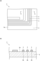
- FIG. 1(a) is a schematic plan view showing a laminated member according to one embodiment of the present invention
- FIG. 1(b) is a schematic cross-sectional view of a portion taken along line AA in FIG. 1(a).
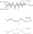
- FIG. 2 is a diagram showing an example of a contour curve in an uneven region of a substrate.
- FIG. 3 is a diagram showing an example of a contour curve in an uneven region of a substrate according to a modified example.
- FIG. 4 is a schematic cross-sectional view showing a base material for lamination according to one embodiment of the present invention.
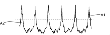
- FIG. 5 is a diagram showing an example of a contour curve in an uneven region of a base material of a comparative example.
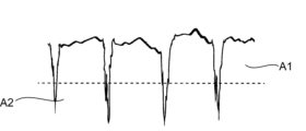
- FIG. 6 is a diagram showing another example of a contour curve in an uneven region of a base material of a comparative example.
- FIG. 1(a) is a schematic plan view showing a laminated member according to an embodiment of the present invention
- Fig. 1(b) is a schematic cross-sectional view of a portion taken along line AA in Fig. 1(a).
- the laminated member 1 includes a base material 2 and an inorganic-containing member 3.
- the inorganic-containing member 3 is provided on the surface 2a of the base material 2.
- the substrate 2 is not particularly limited, and may be, for example, a transparent material.
- transparent materials include glass materials, ceramic materials, and resin materials.
- the substrate 2 is a glass material such as a glass substrate.
- the material of the glass member is not particularly limited, and examples thereof include quartz glass, soda-lime glass, alkali-free glass, aluminosilicate glass, borosilicate glass, fluoride glass, and chalcogenide glass.
- quartz glass soda-lime glass
- alkali-free glass alkali-free glass
- aluminosilicate glass borosilicate glass
- fluoride glass fluoride glass
- chalcogenide glass chalcogenide glass.
- One of these glasses may be used alone, or multiple types may be used in combination.
- the shape of the substrate 2 is not particularly limited, and can be any suitable shape, such as a rectangular plate.
- the thickness of the substrate 2 is not particularly limited, and is preferably 30 ⁇ m or more, more preferably 100 ⁇ m or more, and even more preferably 300 ⁇ m or more, and is preferably 100 mm or less, more preferably 50 mm or less, and even more preferably 20 mm or less.
- the surface 2a of the substrate 2 has an uneven region 2b.
- An inorganic-containing member 3 is laminated on the uneven region 2b of the substrate 2.
- the inorganic-containing member 3 is a metal wiring.
- the inorganic-containing member 3 may be an inorganic-containing member other than a metal wiring, and is not particularly limited.
- the inorganic-containing member 3 may be, for example, a ceramic film such as an oxide film, a nitride film, or a carbide film, or may be a thin metal film such as an electrode film or a magnetic film.
- the electrode film may be, for example, a transparent conductive film such as an ITO film.
- the inorganic-containing member 3 may also form a circuit pattern.
- the inorganic-containing member 3 may also be a paste containing a metal, such as a silver paste.
- the material of the inorganic-containing member 3 is not particularly limited, and may be, for example, a metal, a metal oxide, or a carbon material.
- metals that may be used include aluminum, titanium, gold, silver, copper, chromium, nickel, niobium, tungsten, platinum, and palladium.
- metal oxides that may be used include indium tin oxide (ITO), indium zinc oxide (IZO), and indium gallium zinc oxide (IGZO).
- Examples of carbon materials that may be used include diamond-like carbon (DLC), graphite, and graphene.
- the inorganic-containing member 3 may be a single layer film or a laminated film containing the above materials.
- the inorganic-containing member 3 is provided on a portion of the surface 2a of the substrate 2.
- the area of the inorganic-containing member 3 in a plan view can be in various ranges depending on the desired form, but can be, for example, 5% or more and 90% or less of the total area of the surface 2a of the substrate 2.
- the area of the inorganic-containing member 3 in a plan view is preferably 10% or more, more preferably 20% or more, and even more preferably 30% or more of the total area of the surface 2a of the substrate 2, and is preferably 80% or less, more preferably 70% or less, and even more preferably 60% or less.
- the inorganic-containing member 3 may be provided on the entire surface 2a of the substrate 2.
- the inorganic-containing member 3 is provided on the uneven region 2b of the substrate 2. It is preferable that the inorganic-containing member 3 is selectively provided on the uneven region 2b of the substrate 2. However, a portion of the inorganic-containing member 3 may be provided on an area other than the uneven region 2b. Alternatively, the uneven region 2b may be provided on the entire surface 2a of the substrate 2 or at least a portion thereof, and the inorganic-containing member 3 may be provided on a portion of the uneven region 2b.
- the uneven region 2b is provided only in the region on the surface 2a of the substrate 2 where the inorganic-containing member 3 is laminated.
- the uneven region 2b is provided in a region other than the functional region.
- An example of the functional region is a display region for displaying an image.
- the uneven region 2b is provided only in the region on the surface 2a of the substrate 2 where the inorganic-containing member 3 is laminated.
- the region on the surface 2a of the substrate 2 where the inorganic-containing member 3 is laminated is provided with the uneven region 2b in 90% or more.
- the region on the surface 2a of the substrate 2 where the inorganic-containing member 3 is laminated is provided with the uneven region 2b, preferably 91% or more, more preferably 92% or more, even more preferably 95% or more, and particularly preferably 98% or more.
- the thickness of the inorganic-containing member 3 is not particularly limited and can be, for example, 1 nm or more and 100 ⁇ m or less, preferably 5 nm or more, more preferably 10 nm or more, and preferably 50 ⁇ m or less, more preferably 10 ⁇ m or less.
- the uneven region 2b of the substrate 2 has unevenness in which the average length RSmA of the elements in the contour curve A is 60 nm or more and 1000 nm or less.
- the "average length RSmA of the elements in the contour curve A" is the average length RSmA of the elements in the contour curve A when the measurement length is 5 ⁇ m and the cutoff value of the high-pass filter ⁇ c is set to 2.5 ⁇ m.
- the "average length RSmA of elements in contour curve A” is a parameter defined by JIS B0601:2001, and is a parameter that represents the average distance between adjacent concaves or convexities in contour curve A, which shows the cross-sectional shape of the concaves and convexities.
- the "average length RSmA of elements in contour curve A” is the average of each periodic length of the concaves and convexities in a specified reference length.
- the periodic length of the concaves and convexities is, for example, the length of the part indicated by X in the example of contour curve A shown in Figure 2. Note that hereinafter, the "average length RSmA of elements in contour curve A" may be referred to as the "average length RSmA".
- the inventors focused on the average length RSmA of the contour curve A of the substrate 2 and discovered that by setting the average length RSmA of the contour curve A of the substrate 2 to 60 nm or more and 1000 nm or less, the adhesion between the surface 2a of the substrate 2 and the inorganic-containing member 3 can be increased, thereby suppressing peeling of the inorganic-containing member 3 from the substrate 2.
- the average length RSmA in the contour curve A of the substrate 2 is too small, the contact area between the surface 2a of the substrate 2 and the inorganic-containing member 3 is insufficient, and adhesion is reduced. Also, if the average length RSmA in the contour curve A of the substrate 2 is too large, the recesses in the surface 2a of the substrate 2 will have a shape that spreads horizontally, and the inorganic-containing member 3 will be easily peeled off from the surface 2a of the substrate 2 due to a horizontal force such as scratching.
- the average length RSmA in the contour curve A of the substrate 2 is set to be within the above specific range, it is possible to increase the adhesion between the surface 2a of the substrate 2 and the inorganic-containing member 3, and to suppress peeling of the inorganic-containing member 3 from the substrate 2.
- the average length RSmA in the contour curve A of the substrate 2 is preferably 80 nm or more, more preferably 100 nm or more, even more preferably 120 nm or more, particularly preferably 140 nm or more, and is preferably 900 nm or less, more preferably 800 nm or less, even more preferably 600 nm or less, particularly preferably 500 nm or less.
- the average length RSmA in the contour curve A of the substrate 2 is equal to or greater than the lower limit, the contact area between the surface 2a of the substrate 2 and the inorganic-containing member 3 can be increased, and the adhesion can be further improved.
- the recesses in the surface 2a of the substrate 2 can be made less likely to spread in the horizontal direction, and peeling of the inorganic-containing member 3 due to a horizontal force such as scratching can be made even less likely to occur.
- the maximum valley depth RvA in the contour curve A of the substrate 2 is preferably 10 nm or more, and preferably 500 nm or less.
- maximum valley depth RvA of contour curve A is the maximum valley depth RvA in contour curve A when the measurement length is 5 ⁇ m and the cutoff value of the high-pass filter ⁇ c is set to 2.5 ⁇ m.
- the “maximum valley depth RvA of the contour curve A” is a parameter defined by JIS B0601:2001, and represents the depth of the deepest valley relative to the average line in the contour curve A of the substrate 2.
- the above “average line” is a line obtained by replacing the curve representing the long wavelength components blocked by the high pass filter ⁇ c with a straight line using the least squares method.
- the maximum valley depth RvA in the contour curve A of the substrate 2 is too small, the contact area between the surface 2a of the substrate 2 and the inorganic-containing member 3 that penetrates into the recesses in the surface 2a of the substrate 2 will be small, reducing the anchor effect and making it difficult to obtain sufficient adhesion. Also, if the maximum valley depth RvA in the contour curve A of the substrate 2 is too large, transparency may decrease due to light scattering. Therefore, by setting the maximum valley depth RvA in the contour curve A of the substrate 2 within the above specific range, it is possible to increase the transparency of the laminated member 1 while further suppressing peeling of the inorganic-containing member 3 from the surface 2a of the substrate 2.
- the maximum valley depth RvA in the contour curve A of the substrate 2 is preferably 10 nm or more, more preferably 20 nm or more, even more preferably 30 nm or more, particularly preferably 40 nm or more, and most preferably 50 nm or more, and is preferably 400 nm or less, more preferably 300 nm or less, even more preferably 200 nm or less, and particularly preferably 100 nm or less.
- the maximum valley depth RvA in the contour curve A of the substrate 2 is equal to or greater than the above lower limit, the contact area between the surface 2a of the substrate 2 and the inorganic-containing member 3 can be increased, and the adhesion can be further improved.
- the maximum valley depth RvA is equal to or less than the above upper limit, the transparency of the laminate member 1 can be further improved.
- the ratio (A1/A2) of the upper peak cross-sectional area A1 to the lower valley cross-sectional area A2 of the contour curve A of the substrate 2 from the midline between the highest peak height position and the lowest valley height position is 1.5 or more and 50.0 or less.
- the upper peak cross-sectional area A1 refers to the sum of the cross-sectional areas of all peaks above the midpoint between the highest peak height and the lowest valley height in the profile curve A in the measurement range.
- the lower valley cross-sectional area A2 refers to the sum of the cross-sectional areas of all valleys below the midpoint between the highest peak height and the lowest valley height in the profile curve A in the measurement range.
- the midpoint between the highest peak height and the lowest valley height in the profile curve A is located (RpA-RvA)/2 higher than the average line in the profile curve A (or lower than the average line if (RpA-RvA)/2 is a negative value).
- RpA is the maximum peak height in the profile curve A of the substrate 2, as described below.
- the recesses will be wide and shallow as shown in FIG. 5, the anchor effect will be reduced, and sufficient adhesion may not be obtained.
- the ratio (A1/A2) of the upper peak cross-sectional area A1 to the lower valley cross-sectional area A2 is too large, the region of the recesses will be small as shown in FIG. 6, and sufficient contact area between the surface 2a of the substrate 2 and the inorganic-containing member 3 may not be obtained, and adhesion between the surface 2a of the substrate 2 and the inorganic-containing member 3 may be reduced.
- the ratio (A1/A2) of the upper peak cross-sectional area A1 to the lower valley cross-sectional area A2 is preferably 1.6 or more, more preferably 1.7 or more, even more preferably 1.9 or more, and particularly preferably 2.1 or more, and is preferably 40.0 or less, more preferably 30.0 or less, even more preferably 20.0 or less, and particularly preferably 15.0 or less.
- the ratio (A1/A2) in the contour curve A of the substrate 2 is within the above range, the adhesion between the surface 2a of the substrate 2 and the inorganic-containing member 3 can be further increased, and peeling of the inorganic-containing member 3 from the surface 2a of the substrate 2 can be further suppressed.
- the maximum peak height RpA in the contour curve A of the substrate 2 is preferably 5 nm or more, more preferably 10 nm or more, even more preferably 15 nm or more, and particularly preferably 20 nm or more, and is preferably 400 nm or less, more preferably 300 nm or less, even more preferably 200 nm or less, and particularly preferably 100 nm or less.
- the maximum peak height RpA in the contour curve A of the substrate 2 is within the above range, the adhesion between the surface 2a of the substrate 2 and the inorganic-containing member 3 can be further increased, and peeling of the inorganic-containing member 3 from the surface 2a of the substrate 2 can be further suppressed.
- maximum peak height RpA of profile curve A is the maximum peak height RpA of profile curve A when the measurement length is set to 5 ⁇ m and the cutoff value of the high-pass filter ⁇ c is set to 2.5 ⁇ m, just like the "maximum valley depth RvA of profile curve A.”
- the "maximum peak height RpA of the contour curve A” is a parameter defined by JIS B0601:2001, and represents the height of the highest peak relative to the average line of the contour curve A of the substrate 2.
- the haze of the substrate 2 is not particularly limited and can be selected arbitrarily depending on the desired characteristics and purpose.
- the haze of the substrate 2 is preferably 10% or more, more preferably 15% or more, and even more preferably 20% or more in the wavelength range of 380 nm to 780 nm, and is preferably 95% or less, more preferably 90% or less, and even more preferably 85% or less.
- the haze of the substrate 2 is preferably 0.1% or more, more preferably 0.3% or more, even more preferably 0.5% or more, even more preferably 1% or more in the wavelength range of 380 nm to 780 nm, and is preferably 20% or less, more preferably 15% or less, and even more preferably 10% or less.
- the haze of the substrate 2 is equal to or greater than the above lower limit, the adhesion between the substrate 2 and the inorganic-containing member 3 can be improved more reliably.
- the haze of the substrate 2 is equal to or less than the above upper limit, the transparency of the substrate 2 and therefore the laminate member 1 can be ensured more reliably.
- the inorganic-containing member 3 is less likely to peel off from the surface 2a of the substrate 2.
- Such a laminated member 1 can be suitably used for applications such as touch panel displays, transparent heaters, transparent antennas, and photomasks.
- an original substrate is prepared.
- the unevenness on the surface 2a of the substrate 2 can be formed, for example, by performing a surface treatment such as blasting on the surface on one side of the original substrate.
- Blast treatments such as wet blast treatment and dry sand blast treatment are more suitable for forming fine metal thin films or metal wiring on a substrate 2 such as a glass substrate, since they are easier to treat only the desired areas compared to chemical etching treatments. This allows the transparency of the substrate 2 to be maintained in the required areas by leaving the areas not subjected to surface treatment as untreated areas, for example.
- blasting is a method that makes it easier to increase the maximum valley depth RvA in the contour curve A of the substrate 2.
- the contact area between the substrate 2 and the inorganic-containing member 3 that penetrates into the recesses in the surface 2a of the substrate 2 increases, making it easier to enjoy the anchor effect, and therefore making it easier to improve the adhesion between the substrate 2 and the inorganic-containing member 3.
- the unevenness on the surface 2a of the substrate 2 is preferably formed by performing a surface treatment of wet blasting on one side of the original substrate.
- wet blasting when the slurry is sprayed onto the workpiece, the liquid carries the abrasive grains to the workpiece, making it easier to use finer abrasive grains than in dry sandblasting, and the impact when the abrasive grains collide with the workpiece is smaller, making it possible to perform precise machining.
- wet blasting with a nozzle with a small nozzle area results in less variation during spraying, and is less likely to cause unevenness in the unevenness formed on the substrate 2 compared to dry blasting or chemical etching, making it possible to obtain uniform adhesion with the inorganic-containing member 3.
- Wet blasting is a process in which abrasive grains made of solid particles such as alumina are mixed with liquid such as water to form a slurry, which is then sprayed at high speed from a spray nozzle using compressed air onto the workpiece, which is made of the original base material, to form fine irregularities on the workpiece.
- the abrasive grains sprayed onto the workpiece and the pieces of the workpiece that have been scraped off by the abrasive grains are washed away by the liquid sprayed onto the workpiece, so fewer particles remain on the workpiece.
- the grain size of the abrasive grains can be, for example, an average grain size of 0.3 ⁇ m or more and 60.0 ⁇ m or less.
- the scanning pitch of the nozzle can be, for example, 50 ⁇ m or more and 3000 ⁇ m or less.
- the number of nozzle scans (number of times the same location is scanned) can be, for example, 1 time or more and 10 times or less.
- the ejection pressure of the slurry (processing pressure) can be, for example, 0.10 MPa or more and 0.50 MPa or less.
- the movement speed of the nozzle (processing speed) can be, for example, 0.1 mm/s or more and 100 mm/s or less.
- the average length RSmA, maximum valley depth RvA, and maximum peak height RpA of the elements in the contour curve A of the substrate 2 can be increased.
- the ratio (A1/A2) of the cross-sectional area A1 of the upper peak to the cross-sectional area A2 of the lower valley in the contour curve A of the substrate 2 can be increased.
- the unevenness (uneven region 2b) may be formed on at least a portion of the surface 2a of the substrate 2. It is preferable that the unevenness (uneven region 2b) is formed only on the region of the surface 2a of the substrate 2 where the inorganic-containing member 3 is laminated. By forming the uneven region 2b only on the region where the inorganic-containing member 3 is laminated, unnecessary scattering is less likely to occur in other areas, and transmitted light can be used more effectively. From a similar perspective, if the surface 2a of the substrate 2 has a functional region, it is preferable that the unevenness (uneven region 2b) is formed in a region other than the functional region.
- An example of a functional region is a display region for displaying an image.
- the inorganic-containing member 3 is formed on the uneven region 2b on the surface 2a of the substrate 2.
- Methods for forming the inorganic-containing member 3 include, for example, deposition, ion plating, sputtering, CVD (chemical vapor deposition), screen printing, plating (electroplating, electroless plating, hot-dip plating, thermal spraying), sol-gel, ALD, etc.
- the inorganic-containing member 3 is patterned.
- the inorganic-containing member 3 can be patterned by, for example, photolithography. Specifically, first, a photoresist (hereinafter also simply referred to as resist) is applied onto the inorganic-containing member 3.
- the resist can be applied by, for example, a spin coating method.
- the resist is prebaked to evaporate the solvent and solidify the resist.
- a patterned photomask is placed on the inorganic-containing member 3. For example, a glass mask can be used as the photomask.
- light is irradiated onto the resist through the photomask (exposure process).
- unnecessary resist is removed with a developer to develop the pattern.
- the resist may be negative or positive.
- the inorganic-containing member 3 is patterned by etching using the resist as a mask.
- the etching solution include an aqueous solution of ferric chloride, hydrochloric acid, nitric acid, or an aqueous solution of sodium hydroxide. These etching solutions may be used alone or in combination.
- the resist mask is removed.
- the resist can be removed using an organic solvent such as N-methyl-2-pyrrolidone. In this way, a pattern such as a wiring pattern of the inorganic-containing member 3 is formed.
- a lithography process for forming a resist may be performed first, and then the inorganic-containing member 3 may be laminated to form a pattern such as a wiring pattern of the inorganic-containing member 3.
- a pattern such as a wiring pattern may be directly formed by printing an inorganic-containing member 3 on the uneven region 2b on the surface 2a of the substrate 2 by screen printing, inkjet printing, or the like.
- the inorganic-containing member 3 used for printing include copper paste, silver paste, and gold paste.
- the uneven region 2b of the substrate 2 may further have a second unevenness having an average length RSm of the elements in the contour curve greater than that of the first unevenness, when the unevenness constituting the contour curve A is defined as a first unevenness. More specifically, as shown in Fig. 3, the uneven region 2b of the substrate 2 may have a first unevenness which is a minute unevenness and a second unevenness which is a large unevenness. In this case, the adhesion between the surface 2a of the substrate 2 and the inorganic-containing member 3 can be further increased, and thus peeling of the inorganic-containing member 3 from the substrate 2 can be further suppressed.
- the second irregularity of the substrate 2 has an average element length RSmB in the contour curve B of 3 ⁇ m or more and 50 ⁇ m or less.
- average length RSmB of elements in contour curve B is the average length RSmB of elements in contour curve B when the measured length is 95 ⁇ m, the cutoff value of the high-pass filter ⁇ c is 50 ⁇ m, and the cutoff value of the low-pass filter ⁇ s is 0.8 ⁇ m.
- average length RSmB of elements in contour curve B is a parameter defined by JIS B0601:2001, and is a parameter that represents the average pitch between adjacent concave and convex portions in contour curve B, which shows the cross-sectional shape of the concave and convex portions.
- Average length RSmB of elements in contour curve B is the average of each periodic length of the concave and convex portions in a specified reference length. Each periodic length of the concave and convex portions is, for example, the length of the portion indicated by X2 in the example of contour curve B shown in Figure 3. Note that hereinafter, "average length RSmB of elements in contour curve B" may be referred to as "average length RSmB".
- the average length RSmB of the elements on the contour curve B of the second unevenness of the substrate 2 is too small, the difference with the first unevenness, which is a minute unevenness, becomes small, and the effect of the second unevenness may not be obtained. Also, if the average length RSmB of the elements on the contour curve B of the second unevenness of the substrate 2 is too large, it is difficult to increase the contact area between the surface 2a of the substrate 2 and the inorganic-containing member 3, and adhesion may not be sufficiently improved. Therefore, by setting the average length RSmB of the elements on the contour curve B of the second unevenness of the substrate 2 to be within the above specific range, peeling of the inorganic-containing member 3 from the surface 2a of the substrate 2 can be further suppressed.
- the average length RSmB of the elements on the contour curve B of the second unevenness of the substrate 2 is preferably 3.2 ⁇ m or more, more preferably 3.5 ⁇ m or more, even more preferably 3.7 ⁇ m or more, particularly preferably 4.0 ⁇ m or more, and is preferably 40.0 ⁇ m or less, more preferably 35.0 ⁇ m or less, even more preferably 30.0 ⁇ m or less, particularly preferably 25.0 ⁇ m or less.
- peeling of the inorganic-containing member 3 from the surface 2a of the substrate 2 can be further suppressed.
- the arithmetic mean roughness RaB of the contour curve B of the second irregularity of the substrate 2 is preferably 10 nm or more, and preferably 1000 nm or less.
- the "arithmetic mean roughness RaB of the elements on the contour curve B" is the arithmetic mean roughness RaB on the contour curve B when the measurement length is 95 ⁇ m, the cutoff value of the high-pass filter ⁇ c is 50 ⁇ m, and the cutoff value of the low-pass filter ⁇ s is 0.8 ⁇ m.
- the arithmetic mean roughness RaB on the contour curve B of the second unevenness of the substrate 2 is too small, it is difficult to increase the contact area between the surface 2a of the substrate 2 and the inorganic-containing member 3, and adhesion may not be sufficiently improved. Furthermore, if the arithmetic mean roughness RaB on the contour curve B of the second unevenness of the substrate 2 is too large, transparency may be lost due to scattering. Therefore, by setting the arithmetic mean roughness RaB on the contour curve B of the second unevenness of the substrate 2 within the above specific range, it is possible to further suppress peeling of the inorganic-containing member 3 from the surface 2a of the substrate 2 while maintaining transparency.
- the arithmetic mean roughness RaB on the contour curve B of the second unevenness of the substrate 2 is preferably 10 nm or more, more preferably 15 nm or more, even more preferably 20 nm or more, and particularly preferably 30 nm or more, and is preferably 800 nm or less, more preferably 600 nm or less, even more preferably 400 nm or less, and particularly preferably 200 nm or less.
- peeling of the inorganic-containing member 3 from the surface 2a of the substrate 2 can be further suppressed while maintaining transparency.
- the first and second irregularities in the modified example can be formed by a method including, for example, a first step of forming large preliminary irregularities by subjecting the surface of the original substrate to wet blasting or sand blasting, a second step of subjecting the surface of the original substrate to chemical etching to form second irregularities in the areas where the preliminary irregularities will be provided, and a third step of further subjecting the surface of the original substrate to wet blasting to form minute first irregularities.
- the grain size of the abrasive grains can be, for example, an average grain size of 0.3 ⁇ m or more and 60.0 ⁇ m or less.
- the scanning pitch of the nozzle can be, for example, 50 ⁇ m or more and 3000 ⁇ m or less.
- the number of times the nozzle scans can be, for example, 1 time or more and 10 times or less.
- the ejection pressure of the slurry can be, for example, 0.10 MPa or more and 0.50 MPa or less.
- the movement speed of the nozzle (processing speed) can be, for example, 0.1 mm/s or more and 100 mm/s or less.
- the chemical etching process in the second step can be performed, for example, by immersing the original substrate in hydrofluoric acid or a solution containing hydrofluoric acid and another acid.
- hydrofluoric acid or a solution containing hydrofluoric acid and another acid.
- acids include sulfuric acid, nitric acid, and hydrochloric acid.
- a chelating agent such as citric acid can also be used.
- the content of hydrofluoric acid in the etching solution can be, for example, 0.1% by mass or more and 46% by mass or less.
- the content of sulfuric acid in the etching solution can be, for example, 1% by mass or more and 80% by mass or less.
- the content of water in the etching solution can be, for example, 10% by mass or more and 99.9% by mass or less.
- the temperature of the etching solution can be, for example, 5°C or higher and 80°C or lower.
- the immersion time in the etching solution can be, for example, 10 seconds or higher and 3 hours or lower.
- the etching process may also be performed using hydrogen fluoride gas (HF).
- HF hydrogen fluoride gas
- the grain size of the abrasive grains can be, for example, an average grain size of 0.3 ⁇ m or more and 60.0 ⁇ m or less.
- the scanning pitch of the nozzle can be, for example, 50 ⁇ m or more and 3000 ⁇ m or less.
- the number of times the nozzle scans can be, for example, 1 time or more and 10 times or less.
- the ejection pressure of the slurry can be, for example, 0.10 MPa or more and 0.50 MPa or less.
- the movement speed of the nozzle (processing speed) can be, for example, 0.1 mm/s or more and 100 mm/s or less.
- the average length RSmB and arithmetic mean roughness RaB of the elements in the contour curve B of the second irregularity can be increased by increasing the grain size of the abrasive grains in the wet blasting process in the first step, increasing the processing pressure, or slowing down the nozzle movement speed (processing speed).
- the arithmetic mean roughness RaB of the contour curve B of the second unevenness can be suppressed.
- the immersion time in the etching solution by increasing the immersion time in the etching solution, the average element length RSmB and the arithmetic mean roughness RaB of the contour curve B of the second unevenness can be increased.
- the ratio (A1/A2) of the cross-sectional area A1 of the upper peak to the cross-sectional area A2 of the lower valley in the contour curve A of the first unevenness can be increased.
- FIG. 4 is a schematic cross-sectional view showing a base material for lamination according to one embodiment of the present invention.
- the lamination substrate 10 is a substrate for laminating the inorganic-containing member 3.
- the lamination substrate 10 has the same configuration as the substrate 2 shown in FIG. 1. Therefore, the lamination substrate 10 has an uneven region 2b on the surface 2a, and the uneven region 2b has unevenness in which the average length RSmA of the elements in the contour curve A when the measurement length is 5 ⁇ m and the cutoff value of the high-pass filter ⁇ c is 2.5 ⁇ m is 60 nm or more and 1000 nm or less.
- the surface 2a of the lamination substrate 10 can increase the adhesion with the inorganic-containing member 3, and when the inorganic-containing member 3 is laminated, peeling of the inorganic-containing member 3 from the lamination substrate 10 can be suppressed.
- the uneven region 2b of the lamination substrate 10 may be the region where the inorganic-containing member 3 is provided, and the region 2c on the surface 2a of the lamination substrate 10 other than the uneven region 2b may be the region where the inorganic-containing member 3 is not provided.
- the uneven region 2b of the lamination substrate 10 has the average length RSmA of the elements in the contour curve A described above, so that the adhesion with the inorganic-containing member 3 can be increased, and when the inorganic-containing member 3 is laminated, peeling of the inorganic-containing member 3 from the lamination substrate 10 can be suppressed.
- the surface roughness of the region 2c other than the uneven region 2b of the lamination substrate 10 can be selected arbitrarily depending on the desired characteristics and purpose.
- the lamination substrate 10 may also be a substrate used in photolithography.
- the uneven region 2b of the lamination substrate 10 may be the region where the inorganic-containing member 3 is provided, and the region 2c on the surface 2a of the lamination substrate 10 other than the uneven region 2b may be the region where the inorganic-containing member 3 is removed.
- the uneven region 2b of the lamination substrate 10 has the average element length RSmA in the contour curve A described above, so that the adhesion with the inorganic-containing member 3 can be increased, and when the inorganic-containing member 3 is laminated, the peeling of the inorganic-containing member 3 from the lamination substrate 10 can be suppressed.
- the region 2c other than the uneven region 2b of the lamination substrate 10 does not have the average element length RSmA in the contour curve A described above, so that even when the inorganic-containing member 3 is laminated in the manufacturing process, the inorganic-containing member 3 can be easily removed.
- the lamination substrate 10 may be a substrate used for printing such as screen printing, gravure printing, offset printing, flexographic printing, and inkjet printing.
- the uneven region 2b of the lamination substrate 10 may be the region where the inorganic-containing member 3 is provided, and the region 2c other than the uneven region 2b on the surface 2a of the lamination substrate 10 may be the region where the inorganic-containing member 3 is not provided. Since the uneven region 2b of the lamination substrate 10 has the average length RSmA of the elements in the contour curve A described above, it is possible to increase the adhesion with the inorganic-containing member 3, and when the inorganic-containing member 3 is laminated, it is possible to suppress peeling of the inorganic-containing member 3 from the lamination substrate 10.
- the region 2c other than the uneven region 2b of the lamination substrate 10 the surface roughness can be selected arbitrarily depending on the required characteristics and purpose.
- the uneven region 2b of the lamination substrate 10 is wider than the region in which the inorganic-containing member 3 is provided. In this case, even if the location where the inorganic-containing member 3 is to be provided is slightly shifted during the manufacturing process, the uneven region 2b of the lamination substrate 10 has the average length RSmA of the elements in the contour curve A described above, so that the adhesion with the inorganic-containing member 3 can be increased.
- a region 2c other than the uneven region 2b on the surface 2a of the lamination substrate 10 may have unevenness in which the maximum valley depth RvA in the contour curve A when the measurement length is 5 ⁇ m and the cutoff value of the high-pass filter ⁇ c is 2.5 ⁇ m is 0.1 nm or more and less than 10 nm.
- the area 2c on the surface 2a of the lamination substrate 10 other than the uneven area 2b preferably has unevenness such that the average length RSmA of the elements in the contour curve A when the measurement length is 5 ⁇ m and the cutoff value of the high-pass filter ⁇ c is 2.5 ⁇ m is 0.1 nm or more and less than 60 nm. In this case, even if the inorganic-containing member 3 is laminated in the area 2c other than the uneven area 2b in the manufacturing process, the inorganic-containing member 3 can be removed more easily.
- Examples 1 to 7 First, a rectangular glass plate (aluminosilicate glass, Nippon Electric Glass Co., Ltd., product name "T2X-1") having a thickness of 1.1 mm and obtained by an overflow method was prepared as a substrate material.
- a rectangular glass plate aluminosilicate glass, Nippon Electric Glass Co., Ltd., product name "T2X-1" having a thickness of 1.1 mm and obtained by an overflow method was prepared as a substrate material.
- a slurry was prepared by uniformly stirring 6 wt% abrasive grains and 94 wt% water using alumina abrasive grains with an average particle size of 1.2 ⁇ m, 3.0 ⁇ m, or 4.0 ⁇ m.
- a wet blasting treatment was performed on one of the main surfaces of the glass plate, in which a nozzle with a 1 mm x 1 mm nozzle was moved at 500 ⁇ m intervals to scan the entire surface in a balanced manner at a scanning speed (processing speed) of 20 mm/s, and the processing air pressure was set to 0.1 MPa to 0.3 MPa, and the prepared slurry was sprayed from the nozzle, to produce a substrate.
- the conditions for the wet blasting treatment in Examples 1 to 7 are as shown in Table 1 below.
- Example 8 to 10 In Examples 8 to 10, a preliminary unevenness was imparted to the entire main surface on one side of a glass plate prepared in the same manner as in Example 1 by performing a wet blasting treatment (first wet blasting treatment) and then a chemical etching treatment was performed. Next, a wet blasting treatment (second wet blasting treatment) was performed on the entire main surface on one side of the glass plate after the chemical etching treatment to prepare a substrate.
- first wet blasting treatment first wet blasting treatment
- second wet blasting treatment was performed on the entire main surface on one side of the glass plate after the chemical etching treatment to prepare a substrate.
- a slurry was prepared by uniformly mixing 6 wt% abrasive grains and 94 wt% water using alumina abrasive grains with an average grain size of 1.2 ⁇ m, 6.9 ⁇ m, or 41.1 ⁇ m.
- a wet blasting process was performed in which a nozzle with a 1 mm x 1 mm nozzle was moved and scanned over the entire main surface of one side of the glass plate at a processing speed of 5 mm/s to 50 mm/s, and the processing air pressure was set to 0.15 MPa to 0.32 MPa, and the prepared slurry was sprayed from the nozzle, forming preliminary irregularities with large projections and recesses.
- a slurry was prepared by uniformly mixing 6 wt% abrasive grains and 94 wt% water using alumina abrasive grains with an average grain size of 1.2 ⁇ m.
- a nozzle with a 1 mm x 1 mm nozzle was moved at 500 ⁇ m intervals at a processing speed of 20 mm/s over the entire main surface of the glass plate on which the second irregularities were formed, and the prepared slurry was sprayed from the nozzle at a processing air pressure of 0.2 MPa to 0.3 MPa to form the first irregularities and produce the substrate.
- the conditions for the wet blasting treatment in Examples 8 to 10 are as shown in Table 2 below.
- Comparative Example 1 The glass plate prepared in Example 1 was used as the substrate as it was. Therefore, the substrate in Comparative Example 1 was not subjected to any surface treatment.
- Example 3 A substrate was prepared in the same manner as in Example 9, except that the second wet blasting treatment was not carried out.
- the average length RSmA of the elements in the contour curve A, the maximum valley depth RvA, and the maximum peak height RpA were measured as parameters of the surface roughness to be measured using an atomic force microscope (manufactured by Bruker, product name (SPM unit): Dimension Icon (SPM unit), product name (Controller unit): Nano Scope V (Controller unit)).
- the ratio (A1/A2) of the upper peak cross-sectional area A1 to the lower valley cross-sectional area A2 was calculated from the midline between the highest peak height position and the lowest valley height position in the contour curve A of the substrate.
- the average length RSmB of the elements in the contour curve B and the arithmetic mean roughness RaB were measured as the surface roughness parameters to be measured using a laser microscope (Keyence Corporation, "VK-X250").
- the surface roughness parameters were measured in accordance with JIS B0601:2001.
- the cross section of the laminated member may be observed and the contour curves A and B may be calculated.
- a scanning electron microscope (SEM) or the like may be used after the laminated member is broken.
- Evaluation under condition A was performed using tapping mode, with a measurement area of 5 ⁇ m x 5 ⁇ m, a scan rate of 1 Hz, and 512 x 512 data points.
- the evaluation under condition A was performed by measuring the average length RSmA, maximum valley depth RvA, and maximum peak height RpA of the elements in the profile curve A when the measurement length was set to 5 ⁇ m and the cutoff value of the high-pass filter ⁇ c was set to 2.5 ⁇ m.
- the evaluation under condition B was performed using a 150x objective lens, with the measurement area being 96 ⁇ m x 72 ⁇ m, so that the number of data points acquired was 2048 x 1536.
- the height cut level threshold was set to 50 to remove noise in the height direction, and then analysis was performed.
- the haze was evaluated for the substrates of Examples 1 to 10 and Comparative Examples 1 to 4. The haze was evaluated in the wavelength range of 380 nm to 780 nm. The haze was measured using an ultraviolet-visible-near infrared analyzer photometer (Shimadzu Corporation, product number UV-3100PC) in accordance with JIS K7361-1-1997.
- Example 11 As Example 11, as shown in Table 5, 10% of the area on the surface of the substrate was treated as the uneven area (first area) under the same conditions as the uneven area of Example 3, and the remaining area was treated as the area other than the uneven area of the substrate (second area) in the same manner as in Comparative Example 1. Thereafter, a metal aluminum film was formed on the entire substrate surface with a thickness of 0.3 ⁇ m by a vacuum deposition method. In addition, as Examples 12 to 13, in the combinations shown in Table 5, 10% of the area on the substrate surface was treated as the uneven area (first area) of the substrate surface, and the remaining area was treated as the area other than the uneven area of the substrate surface (second area).
- the maximum valley depth RvA in the contour curve A of the substrate was less than 10 nm and/or the average length RSmA of the elements in the contour curve A of the unevenness of the substrate was less than 60 nm, so the results of the "tape test” and “pencil test” were poor, and the metal aluminum film was easily peeled off from the substrate.
Landscapes
- Laminated Bodies (AREA)
- Surface Treatment Of Glass (AREA)
Priority Applications (2)
| Application Number | Priority Date | Filing Date | Title |
|---|---|---|---|
| JP2025506865A JPWO2024190771A1 (https=) | 2023-03-16 | 2024-03-12 | |
| CN202480007550.8A CN120513167A (zh) | 2023-03-16 | 2024-03-12 | 叠层部件及其制造方法、以及叠层用基材 |
Applications Claiming Priority (2)
| Application Number | Priority Date | Filing Date | Title |
|---|---|---|---|
| JP2023041824 | 2023-03-16 | ||
| JP2023-041824 | 2023-03-16 |
Publications (1)
| Publication Number | Publication Date |
|---|---|
| WO2024190771A1 true WO2024190771A1 (ja) | 2024-09-19 |
Family
ID=92755226
Family Applications (1)
| Application Number | Title | Priority Date | Filing Date |
|---|---|---|---|
| PCT/JP2024/009532 Ceased WO2024190771A1 (ja) | 2023-03-16 | 2024-03-12 | 積層部材及びその製造方法、並びに積層用基材 |
Country Status (3)
| Country | Link |
|---|---|
| JP (1) | JPWO2024190771A1 (https=) |
| CN (1) | CN120513167A (https=) |
| WO (1) | WO2024190771A1 (https=) |
Cited By (1)
| Publication number | Priority date | Publication date | Assignee | Title |
|---|---|---|---|---|
| WO2026070433A1 (ja) * | 2024-09-26 | 2026-04-02 | 日本電気硝子株式会社 | 撥水性部材 |
Citations (6)
| Publication number | Priority date | Publication date | Assignee | Title |
|---|---|---|---|---|
| JPH06302936A (ja) * | 1993-04-14 | 1994-10-28 | Oki Electric Ind Co Ltd | ガラス基板の導体パターン形成方法 |
| JPH0915570A (ja) * | 1995-06-29 | 1997-01-17 | Sharp Corp | 薄膜付ガラス基板 |
| WO2007074610A1 (ja) * | 2005-12-26 | 2007-07-05 | Nippon Electric Glass Co., Ltd. | フラットディスプレイ用ガラス基板 |
| WO2014188918A1 (ja) * | 2013-05-24 | 2014-11-27 | 富士フイルム株式会社 | 透明導電膜及び透明導電膜の製造方法 |
| JP2017199654A (ja) * | 2016-03-15 | 2017-11-02 | パナソニックIpマネジメント株式会社 | 導電性フィルム並びにそれを用いたタッチパネル、ディスプレイ、タッチセンサ及び太陽電池 |
| WO2018047493A1 (ja) * | 2016-09-12 | 2018-03-15 | 富士フイルム株式会社 | 導電性フィルム、タッチパネルセンサー、および、タッチパネル |
-
2024
- 2024-03-12 JP JP2025506865A patent/JPWO2024190771A1/ja active Pending
- 2024-03-12 WO PCT/JP2024/009532 patent/WO2024190771A1/ja not_active Ceased
- 2024-03-12 CN CN202480007550.8A patent/CN120513167A/zh active Pending
Patent Citations (6)
| Publication number | Priority date | Publication date | Assignee | Title |
|---|---|---|---|---|
| JPH06302936A (ja) * | 1993-04-14 | 1994-10-28 | Oki Electric Ind Co Ltd | ガラス基板の導体パターン形成方法 |
| JPH0915570A (ja) * | 1995-06-29 | 1997-01-17 | Sharp Corp | 薄膜付ガラス基板 |
| WO2007074610A1 (ja) * | 2005-12-26 | 2007-07-05 | Nippon Electric Glass Co., Ltd. | フラットディスプレイ用ガラス基板 |
| WO2014188918A1 (ja) * | 2013-05-24 | 2014-11-27 | 富士フイルム株式会社 | 透明導電膜及び透明導電膜の製造方法 |
| JP2017199654A (ja) * | 2016-03-15 | 2017-11-02 | パナソニックIpマネジメント株式会社 | 導電性フィルム並びにそれを用いたタッチパネル、ディスプレイ、タッチセンサ及び太陽電池 |
| WO2018047493A1 (ja) * | 2016-09-12 | 2018-03-15 | 富士フイルム株式会社 | 導電性フィルム、タッチパネルセンサー、および、タッチパネル |
Cited By (1)
| Publication number | Priority date | Publication date | Assignee | Title |
|---|---|---|---|---|
| WO2026070433A1 (ja) * | 2024-09-26 | 2026-04-02 | 日本電気硝子株式会社 | 撥水性部材 |
Also Published As
| Publication number | Publication date |
|---|---|
| CN120513167A (zh) | 2025-08-19 |
| JPWO2024190771A1 (https=) | 2024-09-19 |
Similar Documents
| Publication | Publication Date | Title |
|---|---|---|
| US9279912B2 (en) | Anti-glare glass article and display system | |
| JP5814346B2 (ja) | 防眩表面処理方法およびその物品 | |
| JP5270810B1 (ja) | 電子機器用カバーガラス及びその製造方法、並びにタッチセンサモジュールの製造方法 | |
| JP2013242725A (ja) | トラックパッド用カバーガラス及びその製造方法 | |
| JP7026785B2 (ja) | 高強度指紋防止ガラス、その製造方法、高強度指紋防止ガラスの外装部品およびその製造方法 | |
| CN112125531A (zh) | 玻璃盖板及其制备方法 | |
| CN116400438A (zh) | 玻璃层叠体、显示器用前面板以及显示装置 | |
| CN110712399A (zh) | 玻璃层叠体、显示器用前面板、显示装置和玻璃层叠体的制造方法 | |
| WO2012074811A1 (en) | Anti-glare surface treatment method and articles thereof | |
| JP2003066203A (ja) | 微細凹凸構造の形成方法及び当該凹凸を有する部材 | |
| WO2024190771A1 (ja) | 積層部材及びその製造方法、並びに積層用基材 | |
| CN112250312A (zh) | 微结构的生成方法及表面具有微结构的产品 | |
| JP2013176953A (ja) | 防眩フィルム作製のための金型およびその製造方法 | |
| KR20180069798A (ko) | 디스플레이용 유리 기판 및 그의 제조 방법 | |
| CN111606573A (zh) | 带有凹凸形状的玻璃基体及其制造方法 | |
| WO2020009081A1 (ja) | ガラス板、反射防止層付きガラス板、およびガラス板の製造方法 | |
| TW202006187A (zh) | 附凹凸結構之基體之製造方法 | |
| EP3109211B1 (en) | Surface having properties that reduce light scattering by water condensation and method for the production thereof | |
| JP2003151364A (ja) | 導電膜および導電膜の製造方法 | |
| WO2024095881A1 (ja) | ガラス部材 | |
| KR20240054599A (ko) | 유리소재 회로기판의 디스플레이 모듈 제조방법 | |
| US11994651B2 (en) | Anti-reflective transparent oleophobic surfaces and methods of manufacturing thereof | |
| JP2000258923A (ja) | 酸化錫導電性パタ−ンを形成させる方法 | |
| WO2026070433A1 (ja) | 撥水性部材 | |
| WO2023026971A1 (ja) | 撥水性ガラス部材及びその製造方法、レンズ部材、カバー部材、並びにウインドウパネル部材 |
Legal Events
| Date | Code | Title | Description |
|---|---|---|---|
| 121 | Ep: the epo has been informed by wipo that ep was designated in this application |
Ref document number: 24770876 Country of ref document: EP Kind code of ref document: A1 |
|
| WWE | Wipo information: entry into national phase |
Ref document number: 2025506865 Country of ref document: JP |
|
| WWE | Wipo information: entry into national phase |
Ref document number: 202480007550.8 Country of ref document: CN |
|
| WWP | Wipo information: published in national office |
Ref document number: 202480007550.8 Country of ref document: CN |
|
| NENP | Non-entry into the national phase |
Ref country code: DE |
|
| 122 | Ep: pct application non-entry in european phase |
Ref document number: 24770876 Country of ref document: EP Kind code of ref document: A1 |