WO2024190064A1 - 光検出装置、および、測距システム - Google Patents
光検出装置、および、測距システム Download PDFInfo
- Publication number
- WO2024190064A1 WO2024190064A1 PCT/JP2024/001077 JP2024001077W WO2024190064A1 WO 2024190064 A1 WO2024190064 A1 WO 2024190064A1 JP 2024001077 W JP2024001077 W JP 2024001077W WO 2024190064 A1 WO2024190064 A1 WO 2024190064A1
- Authority
- WO
- WIPO (PCT)
- Prior art keywords
- photodiode
- cathode
- clip
- terminal
- diode
- Prior art date
- Legal status (The legal status is an assumption and is not a legal conclusion. Google has not performed a legal analysis and makes no representation as to the accuracy of the status listed.)
- Ceased
Links
Images












Classifications
-
- G—PHYSICS
- G01—MEASURING; TESTING
- G01J—MEASUREMENT OF INTENSITY, VELOCITY, SPECTRAL CONTENT, POLARISATION, PHASE OR PULSE CHARACTERISTICS OF INFRARED, VISIBLE OR ULTRAVIOLET LIGHT; COLORIMETRY; RADIATION PYROMETRY
- G01J1/00—Photometry, e.g. photographic exposure meter
- G01J1/42—Photometry, e.g. photographic exposure meter using electric radiation detectors
-
- G—PHYSICS
- G01—MEASURING; TESTING
- G01J—MEASUREMENT OF INTENSITY, VELOCITY, SPECTRAL CONTENT, POLARISATION, PHASE OR PULSE CHARACTERISTICS OF INFRARED, VISIBLE OR ULTRAVIOLET LIGHT; COLORIMETRY; RADIATION PYROMETRY
- G01J1/00—Photometry, e.g. photographic exposure meter
- G01J1/42—Photometry, e.g. photographic exposure meter using electric radiation detectors
- G01J1/44—Electric circuits
-
- G—PHYSICS
- G01—MEASURING; TESTING
- G01S—RADIO DIRECTION-FINDING; RADIO NAVIGATION; DETERMINING DISTANCE OR VELOCITY BY USE OF RADIO WAVES; LOCATING OR PRESENCE-DETECTING BY USE OF THE REFLECTION OR RERADIATION OF RADIO WAVES; ANALOGOUS ARRANGEMENTS USING OTHER WAVES
- G01S7/00—Details of systems according to groups G01S13/00, G01S15/00, G01S17/00
- G01S7/48—Details of systems according to groups G01S13/00, G01S15/00, G01S17/00 of systems according to group G01S17/00
- G01S7/483—Details of pulse systems
- G01S7/486—Receivers
- G01S7/4861—Circuits for detection, sampling, integration or read-out
- G01S7/4863—Detector arrays, e.g. charge-transfer gates
-
- H—ELECTRICITY
- H04—ELECTRIC COMMUNICATION TECHNIQUE
- H04N—PICTORIAL COMMUNICATION, e.g. TELEVISION
- H04N25/00—Circuitry of solid-state image sensors [SSIS]; Control thereof
- H04N25/70—SSIS architectures; Circuits associated therewith
-
- H—ELECTRICITY
- H10—SEMICONDUCTOR DEVICES; ELECTRIC SOLID-STATE DEVICES NOT OTHERWISE PROVIDED FOR
- H10F—INORGANIC SEMICONDUCTOR DEVICES SENSITIVE TO INFRARED RADIATION, LIGHT, ELECTROMAGNETIC RADIATION OF SHORTER WAVELENGTH OR CORPUSCULAR RADIATION
- H10F39/00—Integrated devices, or assemblies of multiple devices, comprising at least one element covered by group H10F30/00, e.g. radiation detectors comprising photodiode arrays
- H10F39/10—Integrated devices
- H10F39/12—Image sensors
Definitions
- This technology relates to a photodetector. More specifically, it relates to a photodetector that detects photons and a distance measuring system.
- SPADs Single-Photon Avalanche Diodes
- dToF Direct Time of Flight
- a readout circuit needs to be placed near the SPAD to measure the timing of the start of avalanche multiplication, and the area of the SPAD is limited by the area of the readout circuit.
- the dToF method requires a larger pixel size compared to sensors that detect RGB (Red Green Blue). For these reasons, it is difficult to achieve high resolution with the dToF method. Therefore, a photodetection device has been proposed in which multiple SPADs share a single readout circuit including a recharge transistor and an amplifier (see, for example, Patent Document 1).
- the readout circuit is shared by multiple SPADs to achieve high resolution.
- the multiple SPADs in the shared structure receives light and the cathode voltage drops, current may flow from the SPAD that is not receiving light to the shared node, causing its cathode voltage to also drop. This drop in the cathode voltage of the SPAD that is not receiving light may lengthen the period until recharging is complete, which may result in increased power consumption.
- This technology was developed in light of these circumstances, and aims to reduce power consumption in photodetection devices in which multiple pixels share a circuit.
- This technology has been made to solve the above problems, and its first aspect is a photodetector device including a first photodiode, a second photodiode, a readout circuit that generates a pulse signal in response to a voltage drop at a specified shared node, a first isolation diode inserted between one of the anode and cathode terminals of the first photodiode and the shared node, with a terminal having the same polarity as the one terminal connected to the one terminal, and a second isolation diode inserted between one of the anode and cathode terminals of the second photodiode and the shared node, with a terminal having the same polarity as the one terminal connected to the one terminal.
- This provides the effect of reducing power consumption.
- the first and second photodiodes may be disposed in a light receiving layer in a predetermined pixel substrate, and the readout circuit may be disposed on a first circuit substrate. This provides the effect of facilitating miniaturization of pixels.
- a signal processing unit may be further provided that is disposed on the second circuit board. This has the effect of facilitating miniaturization of pixels.
- the first and second isolation diodes may be disposed on the first circuit board. This provides the effect of facilitating miniaturization of pixels.
- the first and second isolation diodes may be disposed in a wiring layer within the pixel substrate. This has the effect of facilitating miniaturization of pixels.
- a first selection transistor that opens and closes a path between the first isolation diode and the shared node, and a second selection transistor that opens and closes a path between the second isolation diode and the shared node may be further provided. This provides the effect of improving spatial resolution.
- a first clipping circuit that fixes the cathode voltage of the first photodiode and a second clipping circuit that fixes the cathode voltage of the second photodiode may be further provided. This provides the effect of suppressing the decrease in the cathode voltage of non-selected pixels.
- the first clipping circuit may include a first clipping diode
- the second clipping circuit may include a second clipping diode. This provides the effect of suppressing a drop in the cathode voltage of non-selected pixels.
- the first and second clip diodes may be disposed in a wiring layer within the pixel substrate. This has the effect of facilitating miniaturization of pixels.
- the first and second clip diodes may be disposed on the first circuit board. This provides the effect of facilitating miniaturization of pixels.
- the first clip circuit may include a first clip transistor
- the second clip circuit may include a second clip transistor. This has the effect of suppressing a drop in the cathode voltage of non-selected pixels.
- each of the first and second clip transistors may be diode-connected. This has the effect of suppressing a drop in the cathode voltage of non-selected pixels.
- the first clip transistor may fix the cathode voltage of the first photodiode in accordance with a first control signal, and the first clip transistor may fix the cathode voltage of the second photodiode in accordance with a second control signal. This provides the effect of suppressing a decrease in the cathode voltage of non-selected pixels.
- the first and second clip transistors may be disposed in the light receiving layer. This has the effect of facilitating miniaturization of pixels.
- the first and second clip transistors may be disposed on the circuit board. This has the effect of facilitating miniaturization of pixels.
- the cathode of the first photodiode and the cathode of the first isolation diode may be connected, and the cathode of the first photodiode and the cathode of the first isolation diode may be connected. This provides the effect of suppressing the forward current of the photodiode.
- the anode of the first photodiode and the anode of the first isolation diode may be connected, and the anode of the first photodiode and the anode of the first isolation diode may be connected. This provides the effect of suppressing the forward current of the photodiode.
- the second aspect of the present technology is a distance measurement system including a light source that emits an irradiated light, a first photodiode that receives reflected light from the irradiated light, a second photodiode that receives reflected light from the irradiated light, a readout circuit that generates a pulse signal according to a voltage drop at a predetermined shared node, a first isolation diode that is inserted between one of the anode and cathode terminals of the first photodiode and the shared node, with a terminal having the same polarity as the one terminal connected to the one terminal, and a second isolation diode that is inserted between one of the anode and cathode terminals of the second photodiode and the shared node, with a terminal having the same polarity as the one terminal connected to the one terminal.
- This provides the effect of reducing the power consumption of the distance measurement system.
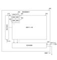
- FIG. 1 is a block diagram showing a configuration example of a distance measuring system according to a first embodiment of the present technology
- 1 is a block diagram showing a configuration example of a solid-state imaging element according to a first embodiment of the present technology
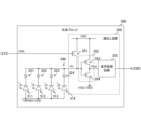
- 3 is a circuit diagram showing a configuration example of a shared block according to the first embodiment of the present technology
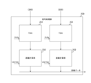
- FIG. 2 is a block diagram showing a configuration example of a signal processing unit according to the first embodiment of the present technology
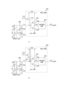
- FIG. FIG. 13 is a circuit diagram showing a configuration example of a shared block in a comparative example. 13 is a diagram for explaining the direction of a current in a shared block in the comparative example.
- FIG. 11 is a diagram for explaining the direction of a current in a shared block in the first embodiment
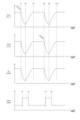
- FIG. 10 is a timing chart showing an example of an operation of a solid-state imaging device in a comparative example.
- 4 is a timing chart showing an example of an operation of the solid-state imaging element according to the first embodiment of the present technology.
- 11 is a circuit diagram of a shared block in which the connection destinations of the anode and cathode are changed according to the first embodiment of the present technology.
- FIG. 1 is a diagram showing an example of a stacked structure of a solid-state imaging element according to a first modified example of the first embodiment of the present technology; 13 is a diagram showing another example of a stacked structure of the solid-state imaging element in the first modified example of the first embodiment of the present technology;
- FIG. 1 is a diagram showing an example of a stacked structure of a solid-state imaging element according to a first modified example of the first embodiment of the present technology
- 13 is a diagram showing another example of a stacked structure of the solid-state imaging element in the first modified example of the first embodiment of the present technology
- FIG. 13 is a diagram showing an example of a stacked structure of a solid-state imaging element according to a second modified example of the first embodiment of the present technology
- FIG. 13 is a diagram showing another example of a stacked structure of a solid-state imaging element in the second modified example of the first embodiment of the present technology
- FIG. 13 is an example of a cross-sectional view of a solid-state imaging element according to a second modified example of the first embodiment of the present technology
- 13 is another example of a cross-sectional view of the solid-state imaging element according to the second modified example of the first embodiment of the present technology.
- FIG. 13 is a circuit diagram showing a configuration example of a shared block according to a second embodiment of the present technology.
- FIG. 13 is a timing chart showing an example of an operation of a solid-state imaging element according to a second embodiment of the present technology.
- FIG. 13 is a circuit diagram showing a configuration example of a shared block according to a third embodiment of the present technology.
- FIG. 13 is a circuit diagram illustrating a configuration example of a shared block in a modified example of the third embodiment of the present technology.
- 13 is an example of a cross-sectional view of a solid-state imaging element according to a modified example of the third embodiment of the present technology.
- FIG. 13 is an example of a cross-sectional view of a solid-state imaging element in a case where a clip diode is arranged on the light receiving side according to a modified example of the third embodiment of the present technology
- 13 is an example of a cross-sectional view of a solid-state imaging element in a case where a clip diode is arranged on a circuit board according to a modified example of the third embodiment of the present technology
- FIG. 13 is a circuit diagram showing a configuration example of a shared block according to a fourth embodiment of the present technology.
- 13 is an example of a cross-sectional view of a solid-state imaging element according to a modified example of the fourth embodiment of the present technology.
- FIG. 13 is another example of a cross-sectional view of a solid-state imaging element according to a modified example of the fourth embodiment of the present technology.
- FIG. 13 is a circuit diagram showing a configuration example of a shared block according to a fifth embodiment of the present technology.
- 1 is a block diagram showing a schematic configuration example of a vehicle control system;
- FIG. 4 is an explanatory diagram showing an example of an installation position of an imaging unit.
- First embodiment (example in which an isolation diode is inserted) 2.
- Second embodiment (an example in which an isolation diode is inserted and a selection transistor is added) 3.
- Third embodiment (an example in which an isolation diode is inserted and a clip diode is added) 4.
- Fourth embodiment (an example in which an isolation diode is inserted and a clip transistor is added) 5.
- Fifth embodiment (an example in which an isolation diode is inserted and a clip transistor is added for individual control) 6. Examples of applications to moving objects
- First embodiment [Example of distance measurement system configuration] 1 is a block diagram showing an example of a configuration of a distance measuring system 100 according to a first embodiment of the present technology.
- the distance measuring system 100 measures the distance to an object, and includes a light source 110, a timing generating unit 120, and a solid-state imaging element 200.
- the distance measuring system 100 is mounted on a smartphone, a personal computer, an in-vehicle device, or the like, and is used to measure distances.
- the timing generation unit 120 generates a timing signal for synchronously operating the light source 110 and the solid-state imaging element 200.
- the timing generation unit 120 generates a clock signal CLKp of a predetermined frequency (e.g., 100 megahertz to 10 gigahertz) as a timing signal, and supplies it to the solid-state imaging element 200 via a signal line 129.
- the timing generation unit 120 also supplies a clock signal CLKd, which is generated in synchronization with the clock signal CLKp, to the light source 110 via a signal line 128.
- the frequency of the clock signal CLKd is 1/P (P is an integer) of the clock signal CLKp.
- the light source 110 supplies intermittent light as irradiation light in synchronization with the clock signal CLKd from the timing generation unit 120.
- intermittent light for example, near-infrared light is used as the irradiation light.
- the solid-state imaging element 200 receives reflected light from the irradiated light and measures the round-trip time from the emission timing indicated by the clock signal CLKd to the timing of receiving the reflected light. This solid-state imaging element 200 calculates the distance to the object from the round-trip time, and generates and outputs distance data indicating that distance.
- the solid-state imaging element 200 is an example of a light detection device as described in the claims.
- solid-state imaging element 200 is provided in the distance measurement system 100, the present invention is not limited to this configuration.
- the solid-state imaging element 200 can also be provided in an imaging device or the like and used to capture image data.
- Example of the configuration of a solid-state imaging element 2 is a block diagram showing an example of a configuration of a solid-state imaging element 200 according to the first embodiment of the present technology.
- the solid-state imaging element 200 includes a control circuit 210, a pixel array unit 220, and a signal processing unit 230.
- the circuits and elements in the solid-state imaging element 200 are arranged on, for example, a single semiconductor substrate.
- shared blocks 300 are arranged in L rows and M columns.
- L is an integer equal to or greater than 1
- M is an integer equal to or greater than 2.
- N pixels N is an integer equal to or greater than 2 that share a portion of the circuit are arranged.
- four pixels, pixels 301, 302, 303, and 304, are arranged in shared block 300 in 2 rows and 2 columns.
- the control circuit 210 controls each of the pixels in the pixel array section 220 based on the clock signal CLKp from the timing generation section 120.
- the signal processing unit 230 measures the round trip time for each pixel based on the signal from the pixel and the clock signal CLKp, and calculates the distance. This signal processing unit 230 generates distance data indicating the distance for each pixel group corresponding to the ranging point, and outputs this data to the outside. Note that the signal processing unit 230 may be disposed inside the pixel array unit 220, or may be disposed outside the pixel array unit 220.
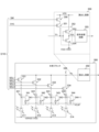
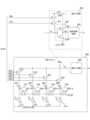
- FIG. 3 is a circuit diagram showing an example of a configuration of a shared block 300 according to the first embodiment of the present technology.
- the shared block 300 includes SPADs 311, 312, 313, and 314, isolation diodes 321, 322, 323, and 324, and a read circuit 350.
- the SPADs 311 to 314 generate electric charges (such as electrons) by photoelectric conversion of incident light, avalanche multiply them, and output them from the cathode.
- a reverse bias with an absolute value greater than the breakdown voltage at the time of avalanche breakdown is applied between the anode and cathode of each of these SPADs.
- a reverse bias voltage VSPAD is applied to the anode of each of the SPADs 311 to 314.
- SPAD311 is an example of a first photodiode as described in the claims
- SPAD312 is an example of a second photodiode as described in the claims.
- Isolation diode 321 is a diode inserted between the cathode of SPAD311 and shared node 349. The cathode of this isolation diode 321 is connected to the cathode of SPAD311. Isolation diode 322 is a diode inserted between the cathode of SPAD312 and shared node 349. The cathode of this isolation diode 322 is connected to the cathode of SPAD312.
- the isolation diode 323 is a diode inserted between the cathode of the SPAD313 and the shared node 349.
- the cathode of this isolation diode 323 is connected to the cathode of the SPAD313.
- the isolation diode 324 is a diode inserted between the cathode of the SPAD314 and the shared node 349.
- the cathode of this isolation diode 324 is connected to the cathode of the SPAD314.
- isolation diode 321 is an example of a first isolation diode described in the claims
- isolation diode 322 is an example of a second isolation diode described in the claims.
- the read circuit 350 generates a pulse signal in response to a voltage drop at the shared node 349.
- This read circuit 350 includes a recharge transistor 351, an amplifier 352, and a signal processing circuit 355.
- the recharge transistor 351 supplies a charging current to each of the SPADs 311 to 314 in accordance with a control signal CHG from the control circuit 210.
- This recharge transistor 351 is inserted between the power supply voltage VDD and the shared node.
- a pMOS (p-channel Metal Oxide Semiconductor) transistor is used as the recharge transistor 351.
- the amplifier 352 amplifies the voltage Vin of the shared node.
- an inverter consisting of a pMOS transistor 353 and an nMOS (n-channel MOS) transistor 354 is used as this amplifier 352. These transistors are inserted in series between the power supply voltage VDD and the reference voltage VSS.
- the amplifier 352 also supplies the voltage Vout, which is obtained by inverting and amplifying Vin, to the signal processing circuit 355.
- the reference voltage VSS is set to a value lower than the power supply voltage VDD.
- the reverse bias voltage VSPAD is set to a value lower than the reference voltage VSS.
- the signal processing circuit 355 adjusts the waveform of the voltage Vout signal to generate a pulse signal. This signal processing circuit 355 supplies the pulse signal to the signal processing unit 230.
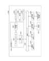
- [Configuration example of signal processing unit] 4 is a block diagram showing an example of a configuration of the signal processing unit 230 according to the first embodiment of the present technology.
- the signal processing unit 230 includes a time-to-digital converter (TDC) 231 and a distance calculation unit 232 for each column of the shared blocks 300 or for each predetermined number of the shared blocks 300.
- TDC time-to-digital converter
- the TDC 231 measures the time from the light emission timing indicated by the clock signal CLKp to the rising edge of the pulse signal from the corresponding column (i.e., the light reception timing). This TDC 231 supplies a digital signal indicating the measured time to the distance calculation unit 232.
- the signal processing unit 230 can also be arranged inside the pixel array unit 220.
- a TDC 231 is arranged below each of a predetermined number of shared blocks 300.
- Example of shared block configuration is a circuit diagram showing a configuration example of a shared block 300 in a comparative example.
- a quench resistor is inserted between the cathode of each of the SPADs 311 to 314 and the shared node 349.
- FIG. 6 is a diagram for explaining the direction of current in the shared block in the comparative example.
- SPADs 313 and 314 and the two corresponding quench resistors are omitted in a and b of the figure.
- a shows an example of the direction of current from the start of avalanche multiplication (in other words, ignition) to quenching.
- a assumes that photons are incident on SPAD312, while no photons are incident on SPAD311.
- SPAD312 ignites, current flows in the reverse bias direction from its cathode to its anode, and the cathode voltage of SPAD312 drops due to the quench resistance. Then, when the reverse bias reaches the breakdown voltage, the avalanche multiplication of SPAD312 stops (in other words, quenches).
- the cathode voltage of SPAD311, where no photons are incident does not initially drop and remains at the initial state of VDD. Therefore, the potential difference between the cathode of SPAD311 and the cathode of SPAD312 causes a forward current to flow from SPAD311 to the shared node 349. This current causes the cathode voltage of the non-firing SPAD311 to drop, dragged along by the firing of SPAD312.
- the hollow arrow marked a in the figure indicates the direction of the current.
- b indicates the direction of the current from immediately after quenching until recharging is complete.
- a pulse signal rises in response to the drop in the cathode voltage, and in response to this rise, control circuit 210 (not shown) transitions control signal CHG from high to low. This causes recharge transistor 351 to transition to the on state, and the supply of charging current from VDD to SPADs 311 and 312, i.e., recharging, begins.
- the white arrows in b in the figure indicate the direction of the current.
- the cathode voltages of SPADs 311 and 312 rise as a result of recharging, and recharging is completed when they reach the original VDD.
- the ignition of SPAD312 causes the cathode voltage of the non-ignited SPAD311 to drop, and the stored charge is discharged from the cathode.
- the recharge time from quench to completion of recharge is longer than in the case where the cathode voltage of SPAD311 does not drop, and power consumption increases accordingly.
- FIG. 7 is a diagram for explaining the direction of current in the shared block 300 in the first embodiment.
- SPADs 313 and 314 and isolation diodes 323 and 324 are omitted in a and b of the figure.
- “a” shows an example of the direction of current flow from ignition to quenching.
- SPAD312 ignites, current flows in the reverse bias direction, as in the comparative example.
- the rectification action of isolation diode 322 between the cathode of SPAD312 and shared node 349 suppresses the forward current from SPAD311 to shared node 349. This suppresses the voltage drop at the cathode of SPAD311 that is not ignited.
- b indicates the direction of the current from immediately after quenching until recharging is completed.
- charging current is supplied from VDD to SPAD 311 and 312.
- the voltage drop at the cathode of the non-ignited SPAD 311 is suppressed, so the recharge time is shorter and power consumption is reduced compared to the comparative example in which the cathode voltage of such a SPAD drops.
- the current flowing through the ignited SPAD and the charging current are not blocked because they are in the forward direction of the isolation diode 321, etc.
- the current flowing from the non-ignited SPAD is in the reverse direction and is therefore blocked by the isolation diode 321, etc.
- [Example of operation of solid-state imaging device] 8 is a timing chart showing an example of the operation of the solid-state imaging device 200 in the comparative example.
- Vca1 indicates the cathode voltage of the SPAD 311
- Vca2 indicates the cathode voltage of the SPAD 312.
- Vin indicates the voltage of the shared node 349 (in other words, the input node of the amplifier 352)
- Vout indicates the voltage of the output node of the amplifier 352. The same applies hereinafter.
- the cathode voltage Vca1 drops due to avalanche multiplication of SPAD311, and is quenched at timing T3. Also, in the comparative example, as described above, the cathode voltage Vca2 of the non-firing SPAD312 also drops due to being pulled down by the ignited SPAD311.
- the voltage Vin of the shared node 349 also drops, and in response to this drop, the voltage Vout output by the amplifier 352 rises at timing T2.
- the voltage Vin also drops, and in response to this drop, the voltage Vout rises at timing T7.
- FIG. 9 is a timing chart showing an example of the operation of the solid-state imaging element 200 in the first embodiment of the present technology.
- the isolation diode 322 suppresses the drop in the cathode voltage Vca2 of the non-ignited SPAD312.
- the cathode voltage Vca1 rises due to recharging, and recharging is completed at timing T5'.
- the voltage Vin also rises, and in response to this rise, the voltage Vout falls at timing T4'.
- the isolation diode 321 suppresses the drop in the cathode voltage Vca1 of the unfired SPAD311.
- the cathode voltage Vca2 rises due to recharging, and recharging is completed at timing T10'.
- the voltage Vin also rises, and in response to this rise, the voltage Vout falls at timing T9'.
- pixels are isolated by isolation diodes 321 and the like, and the drop in the cathode voltage of non-firing SPADs is suppressed, resulting in a shorter recharge time than in the comparative example.
- the recharge time from timing T3 to T5' and the recharge time from timing T8 to T10' are shorter than in the comparative example shown in FIG. 8. This makes it possible to reduce power consumption compared to the comparative example.
- the anode and cathode of the SPADs can be connected inversely.
- isolation diodes 321 to 324 are inserted between the anodes of the SPADs 311 to 314 and the shared node 349, and the anodes of the SPADs 311, etc. and the isolation diodes 321, etc. are connected.
- the nMOS transistor 354 is connected to the VDD side, and the recharge transistor 351 and the pMOS transistor 353 are connected to the VSS side.
- the cathode of the isolation diode 321 etc. is connected to the cathode of the SPAD 311 etc., it is possible to suppress the drop in the cathode voltage of the SPAD that is not ignited. This makes it possible to reduce power consumption.
- the circuits and elements of the solid-state imaging device 200 are arranged on a single semiconductor substrate, but this configuration may make it difficult to miniaturize the pixels.
- the solid-state imaging device 200 in the first modified example of the first embodiment differs from the first embodiment in that the circuits and elements are arranged on two stacked substrates.
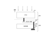
- FIG. 11 is a diagram showing an example of a layered structure of a solid-state imaging element 200 in a first modified example of the first embodiment of the present technology.
- the solid-state imaging element 200 in the first modified example of the first embodiment includes a pixel substrate 201 and a circuit substrate 202 which are layered together.
- the direction from the circuit substrate 202 to the pixel substrate 201 is referred to as the "up" direction.
- the pixel substrate 201 and the circuit substrate 202 are electrically connected by Cu-Cu connections or Au microbumps.
- the pixel substrate 201 includes a light receiving layer 205 in which a plurality of SPADs, such as SPAD 311, are arranged.
- a wiring layer 206 such as a polysilicon layer, is formed below the light receiving layer 205.
- the wiring layer 206 includes a diode layer 207.
- a plurality of isolation diodes, such as isolation diode 321, are arranged in this diode layer 207.
- the circuit board 202 is provided with a subsequent circuit 208, such as a readout circuit 350, a TDC 231, and a distance calculation unit 232 that generates a histogram.
- the diode layer 207 is electrically connected to the subsequent circuit 208 by, for example, a through via 361.
- a counter that counts photons is provided in the subsequent circuit 208.
- the diode layer 207 can also be disposed on the circuit board 202.
- circuits and elements are arranged on the stacked pixel substrate 201 and circuit substrate 202, it is easier to miniaturize pixels than in the first embodiment.
- the circuits and elements of the solid-state imaging device 200 are arranged on a single semiconductor substrate, but this configuration may make it difficult to miniaturize the pixels.
- the solid-state imaging device 200 in the second modified example of the first embodiment differs from the first embodiment in that the circuits and elements are arranged on three stacked substrates.
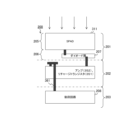
- FIG. 13 is a diagram showing an example of a layered structure of a solid-state imaging element 200 in a second modified example of the first embodiment of the present technology.
- the solid-state imaging element 200 in the second modified example of the first embodiment includes a pixel substrate 201, a circuit substrate 202, and a circuit substrate 203, which are layered.
- the circuit substrate 203 is disposed below the circuit substrate 202. Furthermore, these three substrates are electrically connected by Cu-Cu connections or Au microbumps.
- circuit board 202 is an example of a first circuit board as described in the claims
- circuit board 203 is an example of a second circuit board as described in the claims.
- a plurality of SPADs such as SPAD 311, are arranged in the light receiving layer 205 of the pixel substrate 201.
- a diode layer 207 is disposed in the wiring layer 206 of the pixel substrate 201.
- the amplifier 352 and recharge transistor 351 of the read circuit 350 are arranged on the circuit board 202.
- the diode layer 207 is connected to the amplifier 352 and recharge transistor 351 by a through via 361.
- circuits such as the TDC 231 downstream of the amplifier 352 and the recharge transistor 351 are arranged as the downstream circuit 208.
- the amplifier 352 and the recharge transistor 351 can also be connected to the downstream circuit 208 by a through via 361.
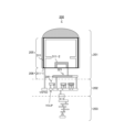
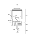
- FIG. 15 is an example of a cross-sectional view of a solid-state imaging element 200 in a second modified example of the first embodiment of the present technology. This figure shows a cross-sectional view of the structure illustrated in FIG. 13.
- the part enclosed in a thick frame in FIG. 15 indicates SPAD311.
- the cathode 311-2 of this SPAD311 is connected to the cathode of the isolation diode 321 in the wiring layer 206.
- a node for the reverse bias voltage VSPAD is provided on the circuit board 202, and the anode 311-1 of SPAD311 is connected to the reverse bias voltage VSPAD.
- isolation diodes such as isolation diode 321 can also be arranged on circuit board 202.
- circuits and elements are arranged on the stacked pixel substrate 201, circuit substrate 202, and circuit substrate 203, it is easier to miniaturize pixels than in the first embodiment.
- Second embodiment In the first embodiment described above, when one or more of the four pixels sharing the readout circuit 350 by a wired-OR connection receive a photon, the readout circuit 350 generates a pulse signal, but this configuration may result in insufficient spatial resolution.
- the solid-state imaging device 200 in this second embodiment differs from the first embodiment in that the path between the shared node 349 and each SPAD is opened and closed individually.
- FIG. 17 is a circuit diagram showing an example of the configuration of a shared block 300 in a second embodiment of the present technology.
- the shared block 300 in this second embodiment differs from the first embodiment in that it further includes selection transistors 331, 332, 333, and 334, and a switch transistor 356.
- selection transistors 331, 332, 333, and 334 selection transistors 331, 332, 333, and 334, and a switch transistor 356.
- pMOS transistors are used as these transistors.
- the selection transistor 331 opens and closes the path between the isolation diode 321 and the shared node 349 in accordance with a selection signal SEL1 from the control circuit 210.
- the selection transistor 332 opens and closes the path between the isolation diode 322 and the shared node 349 in accordance with a selection signal SEL2 from the control circuit 210.
- the selection transistor 333 opens and closes the path between the isolation diode 323 and the shared node 349 in accordance with a selection signal SEL3 from the control circuit 210.
- the selection transistor 334 opens and closes the path between the isolation diode 324 and the shared node 349 in accordance with a selection signal SEL4 from the control circuit 210.
- the switch transistor 356 opens and closes the path between the recharge transistor 351 and the power supply voltage VDD in accordance with a control signal SW from the control circuit 210.
- the control circuit 210 can individually turn on and off each of the selection transistors 331 to 334 using control signals SEL1 to SEL4.
- pixels whose corresponding selection transistors are on are called selected pixels or valid pixels.
- pixels whose corresponding selection transistors are off are called unselected pixels or invalid pixels.
- the readout circuit 350 When some of the four pixels are selected, the readout circuit 350 generates a pulse signal in response to a drop in the cathode voltage of the selected (i.e., active) pixel. On the other hand, even if the cathode voltage of an unselected (i.e., inactive) pixel drops, no pulse signal is generated unless the cathode voltage of the selected pixel drops.
- control circuit 210 can disable the entire shared block 300 and cut off the charging current by controlling the switch transistor 356 to the off state.
- FIG. 18 is a timing chart showing an example of the operation of the solid-state imaging device 200 in the second embodiment of the present technology.
- “a” indicates the fluctuation of the light receiving power and the selection signal.
- “b” indicates valid pixels and invalid pixels.
- the control circuit 210 sets only the selection signal SEL1 of the selection signals SEL1 to SEL4 to a low level.
- the light source 110 (not shown) emits intermittent light as the irradiation light, and the SPADs 311 to 314 receive the reflected light of the irradiation light.
- control circuit 210 sets only the selection signal SEL2 to a low level.
- control circuit 210 sets only the selection signal SEL3 to a low level.
- control circuit 210 sets only the selection signal SEL4 to a low level.
- pixels 301 to 304 are similarly selected one by one in turn.
- control circuit 210 enables one pixel out of four, but it can also enable two or three pixels at the same time, or all four pixels. By enabling some of the four pixels, the spatial resolution of the distance data can be improved compared to when all four pixels are enabled.
- the stacked structures of the first and second variants of the first embodiment can be applied to the second embodiment.
- the selection transistors 331 to 334 are inserted between the shared node 349 and the SPADs 311 to 314, so that some pixels can be enabled to improve the spatial resolution.
- the control circuit 210 individually enables each pixel, but when some of the four pixels are enabled, photons may be incident on an inactive pixel, causing a drop in the cathode voltage due to photoelectric conversion. In this case, the cathode voltage of the inactive pixel continues to drop, and may exceed the withstand voltage of the recharge transistor 351, amplifier 352, and switch transistor 356 in the readout circuit 350, resulting in the element being destroyed.
- the solid-state imaging element 200 in this third embodiment differs from the second embodiment in that the cathode voltage of the inactive pixel is fixed by a clip circuit.
- FIG. 19 is a circuit diagram showing an example of the configuration of the shared block 300 in the third embodiment of the present technology.
- the shared block 300 in the third embodiment differs from the second embodiment in that it further includes clip circuits 341, 342, 343, and 344.
- Clip circuit 341 fixes the cathode voltage of SPAD311.
- Clip circuit 342 fixes the cathode voltage of SPAD312.
- Clip circuit 343 fixes the cathode voltage of SPAD313.
- Clip circuit 344 fixes the cathode voltage of SPAD314.
- Clip circuit 341 for example, includes clip diode 341-1, the cathode of which is connected to the cathode of SPAD311.
- Clip circuit 344 for example, includes clip diode 344-1, the cathode of which is connected to the cathode of SPAD314.
- a clip voltage VCLIP is applied to the anode of each of these clip diodes 341-1 to 344-1.
- the clip voltage VCLIP is set to a voltage that does not exceed the breakdown voltage of the transistors in the shared block 300. For example, it is set to a value that is higher than the reverse bias voltage VSPAD and lower than the power supply voltage VDD.
- the magnitude relationship between the clip voltage VCLIP and the reference voltage VSS is arbitrary.
- clip circuit 341 is an example of a first clip circuit described in the claims
- clip circuit 342 is an example of a second clip circuit described in the claims.
- Clip diode 341-1 is an example of a first clip diode described in the claims
- clip diode 342-1 is an example of a second clip diode described in the claims.
- the clip circuit 341 fixes the cathode voltage of the SPAD 311 to the clip voltage VCLIP. Therefore, even if a photon is incident on an disabled pixel, the drop in the cathode voltage of that pixel can be suppressed. This prevents destruction of elements such as the recharge transistor 351, amplifier 352, and switch transistor 356 in the readout circuit 350, and suppresses defects due to element destruction. The same applies to the other pixels.
- the clip diode 341-1 etc. fixes the corresponding cathode voltage, thereby preventing destruction of the element.
- the circuits and elements of the solid-state imaging device 200 are arranged on a single semiconductor substrate, but this configuration may make it difficult to miniaturize the pixels.
- the solid-state imaging device 200 in this modified example of the third embodiment differs from the third embodiment in that the circuits and elements are arranged on multiple stacked substrates.
- FIG. 20 is a circuit diagram showing an example of the configuration of a shared block 300 in a modified example of the third embodiment of the present technology.
- the solid-state imaging element 200 in the modified example of the third embodiment includes, for example, a pixel substrate 201 and a circuit substrate 202 that are stacked together.
- the SPADs 311 to 314, the isolation diodes 321 to 324, and the clip diodes 341-1 to 344-1 are arranged on the pixel substrate 201.
- the selection transistors 331 to 334 and the circuits following the readout circuit 350 are arranged on the circuit substrate 202.
- circuits and elements can also be arranged on the stacked pixel substrate 201, circuit substrate 202, and circuit substrate 203.
- a plurality of isolation diodes such as isolation diode 321 and a plurality of clip diodes such as clip diode 341-1 can be arranged in wiring layer 206.
- the n-type semiconductor connected to the cathode of the SPAD can be shared by the isolation diode and the clip diode, and can be used as the cathode of each.
- multiple isolation diodes such as isolation diode 321 can be arranged in the wiring layer 206, and multiple clip diodes such as clip diode 341-1 can be arranged in the light receiving layer 205.
- multiple isolation diodes such as isolation diode 321 can be arranged on the wiring layer 206, and multiple clip diodes such as clip diode 341-1 can be arranged on the circuit board 202.
- the circuit board 203 can be eliminated, and the circuits and elements can be arranged on two boards. Furthermore, in each of Figs. 21 to 23, the amplifier 352 and the recharge transistor 351 can be arranged, for example, on the circuit board 202.
- circuits and elements are arranged on multiple stacked substrates, making it easier to miniaturize pixels.
- the cathode voltage is fixed by a clip diode, but a transistor can be used instead of the clip diode.
- the solid-state imaging device 200 in the fourth embodiment differs from the third embodiment in that the cathode voltage is fixed by a transistor.
- FIG. 24 is a circuit diagram showing an example of a configuration of a shared block 300 in a fourth embodiment of the present technology.
- the shared block 300 in this fourth embodiment differs from the third embodiment in that the clip circuits 341 to 344 each include clip transistors 341-2 to 344-2 instead of clip diodes.
- clip transistor 341-2 The source of clip transistor 341-2 is connected to the cathode of SPAD311, and clip voltage VCLIP is applied to the drain. In addition, the gate and drain of clip transistor 341-2 are shorted. In other words, clip transistor 341-2 is diode-connected. The same is true for clip transistors 342-2, 343-2, and 344-2.
- the clip transistor 341-2 etc. fixes the corresponding cathode voltage, thereby preventing destruction of the element.
- the circuits and elements of the solid-state imaging device 200 are arranged on a single semiconductor substrate, but this configuration may make it difficult to miniaturize the pixels.
- the solid-state imaging device 200 in this modified example of the fourth embodiment differs from the fourth embodiment in that the circuits and elements are arranged on multiple stacked substrates.
- FIG. 25 is an example of a cross-sectional view of a solid-state imaging element 200 in a modification of the fourth embodiment of the present technology.
- the solid-state imaging element 200 in the modification of the fourth embodiment includes, for example, a pixel substrate 201, a circuit substrate 202, and a circuit substrate 203, which are stacked together.
- multiple isolation diodes such as isolation diode 321 can be arranged in the wiring layer 206, and multiple clip transistors such as clip transistor 341-2 can be arranged in the light receiving layer 205.
- multiple isolation diodes such as isolation diode 321 can be arranged on wiring layer 206, and multiple clip transistors such as clip transistor 341-2 can be arranged on circuit board 202.
- circuits and elements are arranged on multiple stacked substrates, making it easier to miniaturize pixels.
- the clip transistors 341-2 and the like are diode-connected, but these transistors can also be controlled individually.
- the solid-state imaging device 200 in the fifth embodiment differs from the fourth embodiment in that a control signal is supplied to each gate of the clip transistors 341-2 and the like.
- FIG. 27 is a circuit diagram showing an example of the configuration of a shared block 300 in a fifth embodiment of the present technology.
- the shared block 300 in the fifth embodiment differs from the fourth embodiment in that control signals CLP1 to CLP4 from the control circuit 210 are input to the gates of the clip transistors 341-2 to 344-2, respectively.
- Each of the control signals CLP1 to CLP4 is set to either the clip voltage VCLIP or a predetermined on-voltage that turns the corresponding clip transistor on.
- the control circuit 210 turns off one or more of the selection transistors 331 to 334, the control signal of the clip transistor corresponding to the off-state selection transistor is set to the clip voltage VCLIP.
- the control signal of the clip transistor corresponding to the on-state selection transistor is controlled to a predetermined on-voltage. This fixes the cathode voltage of the SPAD corresponding to the off-state selection transistor, making it possible to suppress an increase in the cathode voltage of an invalid pixel due to leakage current of the selection transistor 331, etc.
- the SPAD of an invalid pixel fires, current flows to the VSPAD side, increasing power consumption, but by preventing the cathode of the invalid pixel from being charged by leakage current, it is possible to suppress the increase in power consumption.
- control circuit 210 supplies a control signal to each of the clip transistors 341-2, etc., so that the cathode voltage of the ineffective pixels can be fixed individually.
- the technology according to the present disclosure can be applied to various products.
- the technology according to the present disclosure may be realized as a device mounted on any type of moving body such as an automobile, an electric vehicle, a hybrid electric vehicle, a motorcycle, a bicycle, a personal mobility device, an airplane, a drone, a ship, or a robot.
- FIG. 28 is a block diagram showing a schematic configuration example of a vehicle control system, which is an example of a mobile object control system to which the technology disclosed herein can be applied.
- the vehicle control system 12000 includes a plurality of electronic control units connected via a communication network 12001.
- the vehicle control system 12000 includes a drive system control unit 12010, a body system control unit 12020, an outside vehicle information detection unit 12030, an inside vehicle information detection unit 12040, and an integrated control unit 12050.
- Also shown as functional components of the integrated control unit 12050 are a microcomputer 12051, an audio/video output unit 12052, and an in-vehicle network I/F (interface) 12053.
- the drive system control unit 12010 controls the operation of devices related to the drive system of the vehicle according to various programs.
- the drive system control unit 12010 functions as a control device for a drive force generating device for generating the drive force of the vehicle, such as an internal combustion engine or a drive motor, a drive force transmission mechanism for transmitting the drive force to the wheels, a steering mechanism for adjusting the steering angle of the vehicle, and a braking device for generating a braking force for the vehicle.
- the body system control unit 12020 controls the operation of various devices installed in the vehicle body according to various programs.
- the body system control unit 12020 functions as a control device for a keyless entry system, a smart key system, a power window device, or various lamps such as headlamps, tail lamps, brake lamps, turn signals, and fog lamps.
- radio waves or signals from various switches transmitted from a portable device that replaces a key can be input to the body system control unit 12020.
- the body system control unit 12020 accepts the input of these radio waves or signals and controls the vehicle's door lock device, power window device, lamps, etc.
- the outside-vehicle information detection unit 12030 detects information outside the vehicle equipped with the vehicle control system 12000.
- the image capturing unit 12031 is connected to the outside-vehicle information detection unit 12030.
- the outside-vehicle information detection unit 12030 causes the image capturing unit 12031 to capture images outside the vehicle, and receives the captured images.
- the outside-vehicle information detection unit 12030 may perform object detection processing or distance detection processing for people, cars, obstacles, signs, or characters on the road surface, based on the received images.
- the imaging unit 12031 is an optical sensor that receives light and outputs an electrical signal according to the amount of light received.
- the imaging unit 12031 can output the electrical signal as an image, or as distance measurement information.
- the light received by the imaging unit 12031 may be visible light, or may be invisible light such as infrared light.
- the in-vehicle information detection unit 12040 detects information inside the vehicle.
- a driver state detection unit 12041 that detects the state of the driver is connected.
- the driver state detection unit 12041 includes, for example, a camera that captures an image of the driver, and the in-vehicle information detection unit 12040 may calculate the driver's degree of fatigue or concentration based on the detection information input from the driver state detection unit 12041, or may determine whether the driver is dozing off.
- the microcomputer 12051 can calculate control target values for the driving force generating device, steering mechanism, or braking device based on information inside and outside the vehicle acquired by the outside vehicle information detection unit 12030 or the inside vehicle information detection unit 12040, and output control commands to the drive system control unit 12010.
- the microcomputer 12051 can perform cooperative control aimed at realizing the functions of an Advanced Driver Assistance System (ADAS), including vehicle collision avoidance or impact mitigation, following driving based on the distance between vehicles, maintaining vehicle speed, vehicle collision warning, or vehicle lane departure warning.
- ADAS Advanced Driver Assistance System
- the microcomputer 12051 can also perform cooperative control for the purpose of autonomous driving, which allows the vehicle to travel autonomously without relying on the driver's operation, by controlling the driving force generating device, steering mechanism, braking device, etc. based on information about the surroundings of the vehicle acquired by the outside vehicle information detection unit 12030 or the inside vehicle information detection unit 12040.
- the microcomputer 12051 can also output control commands to the body system control unit 12020 based on information outside the vehicle acquired by the outside-vehicle information detection unit 12030. For example, the microcomputer 12051 can control the headlamps according to the position of a preceding vehicle or an oncoming vehicle detected by the outside-vehicle information detection unit 12030, and perform cooperative control aimed at preventing glare, such as switching high beams to low beams.
- the audio/image output unit 12052 transmits at least one output signal of audio and image to an output device capable of visually or audibly notifying the occupants of the vehicle or the outside of the vehicle of information.
- an audio speaker 12061, a display unit 12062, and an instrument panel 12063 are exemplified as output devices.
- the display unit 12062 may include, for example, at least one of an on-board display and a head-up display.
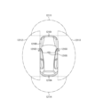
- FIG. 29 shows an example of the installation position of the imaging unit 12031.
- the imaging unit 12031 includes imaging units 12101, 12102, 12103, 12104, and 12105.
- the imaging units 12101, 12102, 12103, 12104, and 12105 are provided, for example, at the front nose, side mirrors, rear bumper, back door, and upper part of the windshield inside the vehicle cabin of the vehicle 12100.
- the imaging unit 12101 provided at the front nose and the imaging unit 12105 provided at the upper part of the windshield inside the vehicle cabin mainly acquire images of the front of the vehicle 12100.
- the imaging units 12102 and 12103 provided at the side mirrors mainly acquire images of the sides of the vehicle 12100.
- the imaging unit 12104 provided at the rear bumper or back door mainly acquires images of the rear of the vehicle 12100.
- the imaging unit 12105 provided at the upper part of the windshield inside the vehicle cabin is mainly used to detect leading vehicles, pedestrians, obstacles, traffic lights, traffic signs, lanes, etc.
- FIG. 29 shows an example of the imaging ranges of the imaging units 12101 to 12104.
- Imaging range 12111 indicates the imaging range of the imaging unit 12101 provided on the front nose
- imaging ranges 12112 and 12113 indicate the imaging ranges of the imaging units 12102 and 12103 provided on the side mirrors, respectively
- imaging range 12114 indicates the imaging range of the imaging unit 12104 provided on the rear bumper or back door.
- an overhead image of the vehicle 12100 viewed from above is obtained by superimposing the image data captured by the imaging units 12101 to 12104.
- At least one of the imaging units 12101 to 12104 may have a function of acquiring distance information.
- at least one of the imaging units 12101 to 12104 may be a stereo camera consisting of multiple imaging elements, or an imaging element having pixels for phase difference detection.
- the microcomputer 12051 can obtain the distance to each solid object within the imaging ranges 12111 to 12114 and the change in this distance over time (relative speed with respect to the vehicle 12100) based on the distance information obtained from the imaging units 12101 to 12104, and can extract as a preceding vehicle, in particular, the closest solid object on the path of the vehicle 12100 that is traveling in approximately the same direction as the vehicle 12100 at a predetermined speed (e.g., 0 km/h or faster). Furthermore, the microcomputer 12051 can set the inter-vehicle distance that should be maintained in advance in front of the preceding vehicle, and perform automatic braking control (including follow-up stop control) and automatic acceleration control (including follow-up start control). In this way, cooperative control can be performed for the purpose of automatic driving, which runs autonomously without relying on the driver's operation.
- automatic braking control including follow-up stop control
- automatic acceleration control including follow-up start control
- the microcomputer 12051 classifies and extracts three-dimensional object data on three-dimensional objects, such as two-wheeled vehicles, ordinary vehicles, large vehicles, pedestrians, utility poles, and other three-dimensional objects, based on the distance information obtained from the imaging units 12101 to 12104, and can use the data to automatically avoid obstacles.
- the microcomputer 12051 distinguishes obstacles around the vehicle 12100 into obstacles that are visible to the driver of the vehicle 12100 and obstacles that are difficult to see.
- the microcomputer 12051 determines the collision risk, which indicates the risk of collision with each obstacle, and when the collision risk is equal to or exceeds a set value and there is a possibility of a collision, it can provide driving assistance for collision avoidance by outputting an alarm to the driver via the audio speaker 12061 or the display unit 12062, or by forcibly decelerating or steering to avoid a collision via the drive system control unit 12010.
- At least one of the imaging units 12101 to 12104 may be an infrared camera that detects infrared rays.
- the microcomputer 12051 can recognize a pedestrian by determining whether or not a pedestrian is present in the image captured by the imaging units 12101 to 12104. The recognition of such a pedestrian is performed, for example, by a procedure of extracting feature points in the image captured by the imaging units 12101 to 12104 as infrared cameras, and a procedure of performing pattern matching processing on a series of feature points that indicate the contour of an object to determine whether or not it is a pedestrian.
- the audio/image output unit 12052 controls the display unit 12062 to superimpose a rectangular contour line for emphasis on the recognized pedestrian.
- the audio/image output unit 12052 may also control the display unit 12062 to display an icon or the like indicating a pedestrian at a desired position.
- the technology of the present disclosure can be applied to the imaging unit 12031.
- the solid-state imaging element 200 of FIG. 2 can be applied to the imaging unit 12031.
- the present technology can also be configured as follows. (1) a first photodiode; A second photodiode; and a read circuit that generates a pulse signal in response to a voltage drop at a predetermined shared node; a first isolation diode inserted between one of an anode and a cathode of the first photodiode and the shared node, the first isolation diode having a terminal having the same polarity as the one terminal connected to the one terminal; a second isolation diode inserted between one of the anode and cathode terminals of the second photodiode and the shared node, the second isolation diode having a terminal having the same polarity as the one terminal connected to the one terminal.
- the first and second photodiodes are disposed in a light receiving layer in a predetermined pixel substrate;
- the photodetector according to (1) wherein the readout circuit is disposed on a first circuit board.
- a first selection transistor that opens and closes a path between the first isolation diode and the shared node;
- a first clipping circuit that fixes a cathode voltage of the first photodiode;
- the first clipping circuit comprises a first clipping diode;
- the first clip transistor fixes a cathode voltage of the first photodiode according to a first control signal; The photodetector device according to (12), wherein the first clip transistor fixes the cathode voltage of the second photodiode in accordance with a second control signal.
- a cathode of the first photodiode and a cathode of the first isolation diode are connected; The photodetector according to any one of (1) to (16), wherein the cathode of the first photodiode and the cathode of the first isolation diode are connected.
- An anode of the first photodiode and an anode of the first isolation diode are connected; The photodetector according to any one of (1) to (16), wherein the anode of the first photodiode and the anode of the first isolation diode are connected.
- a light source that emits irradiation light; a first photodiode that receives reflected light of the irradiated light; a second photodiode that receives reflected light of the irradiated light; a read circuit that generates a pulse signal in response to a voltage drop at a predetermined shared node; a first isolation diode inserted between one of an anode and a cathode of the first photodiode and the shared node, the first isolation diode having a terminal having the same polarity as the one terminal connected to the one terminal; a second isolation diode inserted between one of the anode and cathode terminals of the second photodiode and the shared node, the second isolation diode having a terminal having the same polarity as the one terminal connected to the one terminal.
- REFERENCE SIGNS LIST 100 Distance measuring system 110 Light emitting source 120 Timing generating section 200 Solid-state imaging element 201 Pixel substrate 202, 203 Circuit substrate 205 Light receiving layer 206 Wiring layer 207 Diode layer 208 Subsequent circuit 210 Control circuit 220 Pixel array section 230 Signal processing section 231 TDC 232 Distance calculation unit 300 Shared block 301 to 304 Pixels 311 to 314 SPAD 311-1 Anode 311-2 Cathode 321 to 324 Isolation diodes 331 to 334 Selection transistors 341 to 344 Clipping circuits 341-1, 342-1, 343-1, 344-1 Clipping diodes 341-2, 342-2, 343-2, 344-2 Clipping transistors 350 Readout circuit 351 Recharge transistor 352 Amplifier 353 pMOS transistor 354 nMOS transistor 355 Signal processing circuit 356 Switching transistor 361 Through via 12031 Imaging section
Landscapes
- General Physics & Mathematics (AREA)
- Engineering & Computer Science (AREA)
- Physics & Mathematics (AREA)
- Spectroscopy & Molecular Physics (AREA)
- Computer Networks & Wireless Communication (AREA)
- Signal Processing (AREA)
- Multimedia (AREA)
- Radar, Positioning & Navigation (AREA)
- Remote Sensing (AREA)
- Solid State Image Pick-Up Elements (AREA)
- Optical Radar Systems And Details Thereof (AREA)
- Photometry And Measurement Of Optical Pulse Characteristics (AREA)
- Transforming Light Signals Into Electric Signals (AREA)
Abstract
複数の画素が回路を共有する光検出装置において、消費電力を低減する。 読出し回路は、所定の共有ノードの電圧降下に応じてパルス信号を生成する。第1のフォトダイオードのアノードおよびカソードのうち一方の端子と共有ノードとの間に第1の分離ダイオードが挿入される。第1のフォトダイオードの一方の端子と極性が同一の第1の分離ダイオードの端子がその一方の端子に接続される。第2のフォトダイオードのアノードおよびカソードのうち一方の端子と共有ノードとの間に第2の分離ダイオードが挿入される。第2のフォトダイオードの一方の端子と極性が同一の第2の分離ダイオードの端子がその一方の端子に接続される。
Description
本技術は、光検出装置に関する。詳しくは、光子を検出する光検出装置、および、測距システムに関する。
従来より、測距や撮像を行う装置において、光子を検出するために、SPAD(Single-Photon Avalanche Diode)が利用されている。dToF(direct Time of Flight)方式でSPADを利用する場合、アバランシェ増倍開始のタイミングを測定するためにSPADの近傍に読出し回路を配置する必要があり、その読出し回路の面積によりSPADの面積が律速される。その一方で、dToF方式では、RGB(Red Green Blue)を検知するセンサーと比較して大きな画素サイズが要求される。これらの事情によりdToF方式では高解像度化が困難である。そこで、リチャージトランジスタおよびアンプを含む1つの読出し回路を複数のSPADで共有する光検出装置が提案されている(例えば、特許文献1参照。)。
上述の従来技術では、読出し回路を複数のSPADで共有することにより、高解像度化を図っている。しかしながら、共有構造の複数のSPADのいずれかが光を受光してカソード電圧が降下した場合、受光していないSPADから共有ノードへ電流が流れ、そのカソード電圧も低下してしまうことがある。この受光していないSPADのカソード電圧の低下により、リチャージが完了するまでの期間が長くなり、その分、消費電力が増大するおそれがある。
本技術はこのような状況に鑑みて生み出されたものであり、複数の画素が回路を共有する光検出装置において、消費電力を低減することを目的とする。
本技術は、上述の問題点を解消するためになされたものであり、その第1の側面は、第1のフォトダイオードと、第2のフォトダイオードと、所定の共有ノードの電圧降下に応じてパルス信号を生成する読出し回路と、上記第1のフォトダイオードのアノードおよびカソードのうち一方の端子と上記共有ノードとの間に挿入され、上記一方の端子と極性が同一の端子が上記一方の端子に接続された第1の分離ダイオードと、上記第2のフォトダイオードのアノードおよびカソードのうち一方の端子と上記共有ノードとの間に挿入され、上記一方の端子と極性が同一の端子が上記一方の端子に接続された第2の分離ダイオードとを具備する光検出装置である。これにより、消費電力が低減するという作用をもたらす。
また、この第1の側面において、上記第1および第2のフォトダイオードは所定の画素基板内の受光層に配置され、上記読出し回路は、第1の回路基板に配置されてもよい。これにより、画素の微細化が容易になるという作用をもたらす。
また、この第1の側面において、第2の回路基板に配置された信号処理部をさらに具備してもよい。これにより、画素の微細化が容易になるという作用をもたらす。
また、この第1の側面において、上記第1および第2の分離ダイオードは、上記第1の回路基板に配置されてもよい。これにより、画素の微細化が容易になるという作用をもたらす。
また、この第1の側面において、上記第1および第2の分離ダイオードは上記画素基板内の配線層に配置されてもよい。これにより、画素の微細化が容易になるという作用をもたらす。
また、この第1の側面において、上記第1の分離ダイオードと上記共有ノードとの間の経路を開閉する第1の選択トランジスタと、上記第2の分離ダイオードと上記共有ノードとの間の経路を開閉する第2の選択トランジスタとをさらに具備してもよい。これにより、空間解像度が向上するという作用をもたらす。
また、この第1の側面において、第1のフォトダイオードのカソード電圧を固定する第1のクリップ回路と、上記第2のフォトダイオードのカソード電圧を固定する第2のクリップ回路とをさらに具備してもよい。これにより、非選択の画素のカソード電圧の低下が抑制されるという作用をもたらす。
また、この第1の側面において、上記第1のクリップ回路は第1のクリップダイオードを備え、上記第2のクリップ回路は第2のクリップダイオードを備えてもよい。これにより、非選択の画素のカソード電圧の低下が抑制されるという作用をもたらす。
また、この第1の側面において、上記第1および第2のクリップダイオードは上記画素基板内の配線層に配置されてもよい。これにより、画素の微細化が容易になるという作用をもたらす。
また、この第1の側面において、上記第1および第2のクリップダイオードは上記受光層に配置されてもよい。これにより、画素の微細化が容易になるという作用をもたらす。
また、この第1の側面において、上記第1および第2のクリップダイオードは上記第1の回路基板に配置されてもよい。これにより、画素の微細化が容易になるという作用をもたらす。
また、この第1の側面において、上記第1のクリップ回路は第1のクリップトランジスタを備え、上記第2のクリップ回路は第2のクリップトランジスタを備えてもよい。これにより、非選択の画素のカソード電圧の低下が抑制されるという作用をもたらす。
また、この第1の側面において、上記第1および第2のクリップトランジスタのそれぞれは、ダイオード接続されてもよい。これにより、非選択の画素のカソード電圧の低下が抑制されるという作用をもたらす。
また、この第1の側面において、上記第1のクリップトランジスタは、第1の制御信号に従って上記第1のフォトダイオードのカソード電圧を固定し、上記第1のクリップトランジスタは、第2の制御信号に従って上記第2のフォトダイオードのカソード電圧を固定してもよい。これにより、非選択の画素のカソード電圧の低下が抑制されるという作用をもたらす。
また、この第1の側面において、上記第1および第2のクリップトランジスタは上記受光層に配置されてもよい。これにより、画素の微細化が容易になるという作用をもたらす。
また、この第1の側面において、上記第1および第2のクリップトランジスタは上記回路基板に配置されてもよい。これにより、画素の微細化が容易になるという作用をもたらす。
また、この第1の側面において、上記第1のフォトダイオードのカソードと上記第1の分離ダイオードのカソードとが接続され、上記第1のフォトダイオードのカソードと上記第1の分離ダイオードのカソードとが接続されてもよい。これにより、フォトダイオードの順方向の電流が抑制されるという作用をもたらす。
また、この第1の側面において、上記第1のフォトダイオードのアノードと上記第1の分離ダイオードのアノードとが接続され、上記第1のフォトダイオードのアノードと上記第1の分離ダイオードのアノードとが接続されてもよい。これにより、フォトダイオードの順方向の電流が抑制されるという作用をもたらす。
また、本技術の第2の側面は、照射光を照射する光源と、上記照射光に対する反射光を受光する第1のフォトダイオードと、上記照射光に対する反射光を受光する第2のフォトダイオードと、所定の共有ノードの電圧降下に応じてパルス信号を生成する読出し回路と、上記第1のフォトダイオードのアノードおよびカソードのうち一方の端子と上記共有ノードとの間に挿入され、上記一方の端子と極性が同一の端子が上記一方の端子に接続された第1の分離ダイオードと、上記第2のフォトダイオードのアノードおよびカソードのうち一方の端子と上記共有ノードとの間に挿入され、上記一方の端子と極性が同一の端子が上記一方の端子に接続された第2の分離ダイオードとを具備する測距システムである。これにより、測距システムの消費電力が低減するという作用をもたらす。
以下、本技術を実施するための形態(以下、実施の形態と称する)について説明する。説明は以下の順序により行う。
1.第1の実施の形態(分離ダイオードを挿入した例)
2.第2の実施の形態(分離ダイオードを挿入し、選択トランジスタを追加した例)
3.第3の実施の形態(分離ダイオードを挿入し、クリップダイオードを追加した例)
4.第4の実施の形態(分離ダイオードを挿入し、クリップトランジスタを追加した例)
5.第5の実施の形態(分離ダイオードを挿入し、クリップトランジスタを追加して個別に制御する例)
6.移動体への応用例
1.第1の実施の形態(分離ダイオードを挿入した例)
2.第2の実施の形態(分離ダイオードを挿入し、選択トランジスタを追加した例)
3.第3の実施の形態(分離ダイオードを挿入し、クリップダイオードを追加した例)
4.第4の実施の形態(分離ダイオードを挿入し、クリップトランジスタを追加した例)
5.第5の実施の形態(分離ダイオードを挿入し、クリップトランジスタを追加して個別に制御する例)
6.移動体への応用例
<1.第1の実施の形態>
[測距システムの構成例]
図1は、本技術の第1の実施の形態における測距システム100の一構成例を示すブロック図である。この測距システム100は、物体までの距離を測定するものであり、発光源110、タイミング生成部120および固体撮像素子200を備える。測距システム100は、スマートフォン、パーソナルコンピュータや車載機器などに搭載され、距離を測定するために用いられる。
[測距システムの構成例]
図1は、本技術の第1の実施の形態における測距システム100の一構成例を示すブロック図である。この測距システム100は、物体までの距離を測定するものであり、発光源110、タイミング生成部120および固体撮像素子200を備える。測距システム100は、スマートフォン、パーソナルコンピュータや車載機器などに搭載され、距離を測定するために用いられる。
タイミング生成部120は、発光源110および固体撮像素子200を同期して動作させるためのタイミング信号を生成するものである。このタイミング生成部120は、タイミング信号として、所定周波数(100メガヘルツ乃至10ギガヘルツなど)のクロック信号CLKpを生成し、固体撮像素子200に信号線129を介して供給する。また、タイミング生成部120は、クロック信号CLKpと同期して生成されたクロック信号CLKdを発光源110に信号線128を介して供給する。クロック信号CLKdの周波数は、クロック信号CLKpの1/P(Pは、整数)である。
発光源110は、タイミング生成部120からのクロック信号CLKdに同期して間欠光を照射光として供給するものである。例えば、照射光として近赤外光などが用いられる。
固体撮像素子200は、照射光に対する反射光を受光し、クロック信号CLKdの示す発光タイミングから反射光を受光したタイミングまでの往復時間を測定するものである。この固体撮像素子200は、物体までの距離を往復時間から算出し、その距離を示す距離データを生成して出力する。なお、固体撮像素子200は、特許請求の範囲に記載の光検出装置の一例である。
なお、固体撮像素子200を測距システム100に設けているが、この構成に限定されない。固体撮像素子200を撮像装置などに設けて、画像データの撮像に用いることもできる。
[固体撮像素子の構成例]
図2は、本技術の第1の実施の形態における固体撮像素子200の一構成例を示すブロック図である。この固体撮像素子200は、制御回路210、画素アレイ部220および信号処理部230を備える。固体撮像素子200内の回路や素子は、例えば、単一の半導体基板に配置される。
図2は、本技術の第1の実施の形態における固体撮像素子200の一構成例を示すブロック図である。この固体撮像素子200は、制御回路210、画素アレイ部220および信号処理部230を備える。固体撮像素子200内の回路や素子は、例えば、単一の半導体基板に配置される。
画素アレイ部220には、L行×M列の共有ブロック300が配列される。ここで、Lは、1以上の整数であり、Mは2以上の整数である。共有ブロック300のそれぞれには、一部の回路を共有するN(Nは、2以上の整数)個の画素が配列される。例えば、画素301、302、303および304の4画素が2行×2列で共有ブロック300に配列される。
制御回路210は、タイミング生成部120からのクロック信号CLKpに基づいて画素アレイ部220内の画素のそれぞれを制御するものである。
信号処理部230は、画素からの信号とクロック信号CLKpとに基づいて画素ごとに往復時間を測定し、距離を算出するものである。この信号処理部230は、距離を示す距離データを測距点に対応する画素群ごとに生成し、それらを外部に出力する。なお、信号処理部230は、画素アレイ部220内に配置されても構わないし、画素アレイ部220の外に配置されても構わない。
[共有ブロックの構成例]
図3は、本技術の第1の実施の形態における共有ブロック300の一構成例を示す回路図である。この共有ブロック300は、SPAD311、312、313および314と、分離ダイオード321、322、323および324と、読出し回路350とを備える。
図3は、本技術の第1の実施の形態における共有ブロック300の一構成例を示す回路図である。この共有ブロック300は、SPAD311、312、313および314と、分離ダイオード321、322、323および324と、読出し回路350とを備える。
SPAD311乃至314は、入射光に対する光電変換により電荷(電子など)を生成し、アバランシェ増倍してカソードから出力するものである。これらのSPADのそれぞれのアノードとカソードとの間には、アバランシェ降伏するときの降伏電圧よりも絶対値が大きな逆バイアスが印加されている。また、SPAD311乃至314のそれぞれのアノードには、逆バイアス電圧VSPADが印加される。
なお、SPAD311は、特許請求の範囲に記載の第1のフォトダイオードの一例であり、SPAD312は、特許請求の範囲に記載の第2のフォトダイオードの一例である。
分離ダイオード321は、SPAD311のカソードと共有ノード349との間に挿入されるダイオードである。この分離ダイオード321のカソードは、SPAD311のカソードと接続される。分離ダイオード322は、SPAD312のカソードと共有ノード349との間に挿入されるダイオードである。この分離ダイオード322のカソードは、SPAD312のカソードと接続される。
分離ダイオード323は、SPAD313のカソードと共有ノード349との間に挿入されるダイオードである。この分離ダイオード323のカソードは、SPAD313のカソードと接続される。分離ダイオード324は、SPAD314のカソードと共有ノード349との間に挿入されるダイオードである。この分離ダイオード324のカソードは、SPAD314のカソードと接続される。
なお、分離ダイオード321は、特許請求の範囲に記載の第1の分離ダイオードの一例であり、分離ダイオード322は、特許請求の範囲に記載の第2の分離ダイオードの一例である。
読出し回路350は、共有ノード349の電圧降下に応じてパルス信号を生成するものである。この読出し回路350は、リチャージトランジスタ351、アンプ352および信号処理回路355を備える。
リチャージトランジスタ351は、制御回路210からの制御信号CHGに従って、SPAD311から314のそれぞれに充電電流を供給するものである。このリチャージトランジスタ351は、電源電圧VDDと共有ノードとの間に挿入される。また、リチャージトランジスタ351として、例えば、pMOS(p-channel Metal Oxide Semiconductor)トランジスタが用いられる。
アンプ352は、共有ノードの電圧Vinを増幅するものである。このアンプ352として、例えば、pMOSトランジスタ353およびnMOS(n-channel MOS)トランジスタ354からなるインバータが用いられる。これらのトランジスタは、電源電圧VDDと基準電圧VSSとの間に直列に挿入される。また、アンプ352は、Vinを反転増幅した電圧Voutを信号処理回路355に供給する。
基準電圧VSSには、電源電圧VDDより低い値が設定される。また、逆バイアス電圧VSPADには、基準電圧VSSより低い値が設定される。
信号処理回路355は、電圧Voutの信号の波形を調整して、パルス信号を生成するものである。この信号処理回路355は、パルス信号を信号処理部230に供給する。
[信号処理部の構成例]
図4は、本技術の第1の実施の形態における信号処理部230の一構成例を示すブロック図である。この信号処理部230は、共有ブロック300の列ごと、または、所定数の共有ブロック300毎にTDC(Time-to-Digital Converter)231および距離計算部232を備える。
図4は、本技術の第1の実施の形態における信号処理部230の一構成例を示すブロック図である。この信号処理部230は、共有ブロック300の列ごと、または、所定数の共有ブロック300毎にTDC(Time-to-Digital Converter)231および距離計算部232を備える。
TDC231は、クロック信号CLKpの示す発光タイミングから、対応する列からのパルス信号の立上り(すなわち、受光タイミング)までの時間を計測するものである。このTDC231は、測定した時間を示すデジタル信号を距離計算部232に供給する。
距離計算部232は、TDCの結果毎にヒストグラムを蓄積するものである。この距離計算部232は、クロック信号CLKpよりも低い周波数の周期ごとに、その周期内でTDC231により計測されたヒストグラムを出力する。なお、距離計算部232は、次の式を用いて距離Dを算出し、その距離Dを示す距離データを出力することもある。
D=(c×dt0)/2
上式において、cは光速であり、単位は、メートル毎秒(m/s)である。また、距離Dの単位は、例えば、メートル(m)であり、往復時間dt0の単位は、例えば、秒(s)である。
D=(c×dt0)/2
上式において、cは光速であり、単位は、メートル毎秒(m/s)である。また、距離Dの単位は、例えば、メートル(m)であり、往復時間dt0の単位は、例えば、秒(s)である。
なお、画素アレイ部220内に信号処理部230を配置することもできる。この場合には、所定数の共有ブロック300ごとに、その下部にTDC231が配置される。
ここで、分離ダイオード321から324の代わりに、クウェンチ抵抗を挿入した構成を比較例として想定する。
[共有ブロックの構成例]
図5は、比較例における共有ブロック300の一構成例を示す回路図である。この比較例の共有ブロック300においては、SPAD311から314のそれぞれのカソードと、共有ノード349との間に、クウェンチ抵抗が挿入される。
図5は、比較例における共有ブロック300の一構成例を示す回路図である。この比較例の共有ブロック300においては、SPAD311から314のそれぞれのカソードと、共有ノード349との間に、クウェンチ抵抗が挿入される。
図6は、比較例における共有ブロック内の電流の方向を説明するための図である。同図におけるaおよびbでは、説明の便宜上、SPAD313および314と、対応する2つのクウェンチ抵抗とを省略している。
同図におけるaは、アバランシェ増倍の開始(言い換えれば、発火)からクウェンチまでの間の電流の方向の一例を示す。同図におけるaにおいて、SPAD312に光子が入射し、その一方でSPAD311には光子が入射していないものとする。このとき、SPAD312は発火し、そのカソードからアノードへの逆バイアス方向に電流が流れ、クウェンチ抵抗によりSPAD312のカソード電圧が降下する。そして、逆バイアスがブレークダウン電圧に達すると、SPAD312のアバランシェ増倍が停止(言い換えれば、クウェンチ)する。
一方、光子が入射しないSPAD311のカソード電圧は、当初は降下しておらず、初期状態のVDDのままである。このため、SPAD311のカソードと、SPAD312のカソードとの間の電位差により、SPAD311から共有ノード349へ順方向に電流が流れてしまう。この電流により、SPAD312の発火に引きずられて、発火していないSPAD311のカソード電圧も降下してしまう。同図におけるaの白抜きの矢印は、電流の方向を示す。
同図におけるbは、クウェンチ直後からリチャージ完了までの間の電流の方向を示す。カソード電圧の降下に応じてパルス信号が立ち上がり、その立ち上がりに応じて制御回路210(不図示)は、制御信号CHGをハイレベルからローレベルに遷移させる。これにより、リチャージトランジスタ351がオン状態に移行して、VDDからSPAD311および312への充電電流の供給、すなわちリチャージが開始される。同図におけるbの白抜きの矢印は、電流の方向を示す。リチャージによりSPAD311および312のそれぞれのカソード電圧は上昇し、元のVDDに達した時点でリチャージが完了する。
上述したように、比較例ではSPAD312の発火に引きずられて、発火していないSPAD311のカソード電圧も降下し、そのカソードから、充電された電荷が放電してしまう。このため、SPAD311のカソード電圧が降下しない場合と比較して、クウェンチからリチャージ完了までのリチャージ時間が長くなり、その分だけ消費電力が増大してしまう。
図7は、第1の実施の形態における共有ブロック300内の電流の方向を説明するための図である。同図におけるaおよびbでは、説明の便宜上、SPAD313および314と、分離ダイオード323および324とを省略している。
同図におけるaは、発火からクウェンチまでの間の電流の方向の一例を示す。SPAD312が発火すると、比較例と同様に逆バイアス方向に電流が流れる。一方、SPAD312のカソードと、共有ノード349との間の分離ダイオード322の整流作用により、SPAD311から共有ノード349への順方向の電流が抑制される。このため、発火していないSPAD311のカソードの電圧降下が抑制される。
同図におけるbは、クウェンチ直後からリチャージ完了までの間の電流の方向を示す。第1の実施の形態においても比較例と同様にVDDからSPAD311および312への充電電流が供給される。
第1の実施の形態では、発火していないSPAD311のカソードの電圧降下が抑制されるため、そのようなSPADのカソード電圧が降下してしまう比較例よりもリチャージ時間が短くなり、消費電力が低減する。
また、同図に例示するように、発火したSPADに流れる電流、および、充電電流は、分離ダイオード321等の順方向であるため、妨げられない。一方で、発火していないSPADから流れる電流は逆方向であるため、分離ダイオード321等により遮断される。
[固体撮像素子の動作例]
図8は、比較例における固体撮像素子200の動作の一例を示すタイミングチャートである。同図においてVca1は、SPAD311のカソード電圧を示し、Vca2は、SPAD312のカソード電圧を示す。Vinは、共有ノード349(言い換えれば、アンプ352の入力ノード)の電圧を示し、Voutは、アンプ352の出力ノードの電圧を示す。以降においても同様である。
図8は、比較例における固体撮像素子200の動作の一例を示すタイミングチャートである。同図においてVca1は、SPAD311のカソード電圧を示し、Vca2は、SPAD312のカソード電圧を示す。Vinは、共有ノード349(言い換えれば、アンプ352の入力ノード)の電圧を示し、Voutは、アンプ352の出力ノードの電圧を示す。以降においても同様である。
タイミングT1において、SPAD311に光子が入射し、その時点でSPAD312には入射していないものとする。このとき、SPAD311のアバランシェ増倍により、カソード電圧Vca1が降下し、タイミングT3でクウェンチする。また、比較例では、上述したように発火したSPAD311に引きずられて、発火していないSPAD312のカソード電圧Vca2も降下してしまう。
また、共有ノード349の電圧Vinも同様に降下し、その降下に応じてタイミングT2でアンプ352の出力する電圧Voutが立ち上がる。
そして、リチャージによりカソード電圧Vca1およびVca2が上昇し、タイミングT5でリチャージが完了する。また、電圧Vinも同様に上昇し、その上昇に応じてタイミングT4で電圧Voutが立ち下がる。
次に、タイミングT6において、SPAD312に光子が入射し、その時点でSPAD311には入射していないものとする。このとき、SPAD312のアバランシェ増倍により、カソード電圧Vca2が降下し、タイミングT8でクウェンチする。また、発火したSPAD312に引きずられて、発火していないSPAD311のカソード電圧Vca1も降下してしまう。
また、電圧Vinも同様に降下し、その降下に応じてタイミングT7で電圧Voutが立ち上がる。
そして、リチャージによりカソード電圧Vca1およびVca2が上昇し、タイミングT10でリチャージが完了する。また、電圧Vinも同様に上昇し、その上昇に応じてタイミングT9で電圧Voutが立ち下がる。
図9は、本技術の第1の実施の形態における固体撮像素子200の動作の一例を示すタイミングチャートである。
タイミングT1において、SPAD311に光子が入射し、その時点でSPAD312には入射していないものとする。このとき、SPAD311のアバランシェ増倍により、カソード電圧Vca1が降下し、タイミングT3でクウェンチする。一方、第1の実施の形態では、分離ダイオード322により、発火していないSPAD312のカソード電圧Vca2の降下が抑制される。
また、カソード電圧Vca1の降下に伴って共有ノード349の電圧Vinが降下し、その降下に応じてタイミングT2で電圧Voutが立ち上がる。
そして、リチャージによりカソード電圧Vca1が上昇し、タイミングT5'でリチャージが完了する。また、電圧Vinも同様に上昇し、その上昇に応じてタイミングT4'で電圧Voutが立ち下がる。
次に、タイミングT6において、SPAD312に光子が入射し、その時点でSPAD311には入射していないものとする。このとき、SPAD312のアバランシェ増倍により、カソード電圧Vca2が降下し、タイミングT8でクウェンチする。一方、第1の実施の形態では、分離ダイオード321により、発火していないSPAD311のカソード電圧Vca1の降下が抑制される。
また、カソード電圧Vca2の降下に伴って共有ノード349の電圧Vinが降下し、その降下に応じてタイミングT7で電圧Voutが立ち上がる。
そして、リチャージによりカソード電圧Vca2が上昇し、タイミングT10'でリチャージが完了する。また、電圧Vinも同様に上昇し、その上昇に応じてタイミングT9'で電圧Voutが立ち下がる。
同図に例示したように、第1の実施の形態では、分離ダイオード321等により画素が分離され、発火していないSPADのカソード電圧の降下が抑制されるため、比較例よりもリチャージ時間が短くなる。同図においては、タイミングT3からT5'までのリチャージ時間と、タイミングT8からT10'のリチャージ時間とが図8に例示した比較例よりも短くなる。これにより、比較例と比較して消費電力を低減することができる。
なお、図10に例示するように、SPADのアノード、カソードの接続先を逆にすることもできる。同図においては、SPAD311から314のそれぞれのアノードと共有ノード349との間に、分離ダイオード321から324が挿入され、SPAD311等のアノードと、分離ダイオード321等のアノードとが接続される。また、nMOSトランジスタ354は、VDD側に接続され、リチャージトランジスタ351およびpMOSトランジスタ353は、VSS側に接続される。
このように、本技術の第1の実施の形態によれば、SPAD311等のカソードに分離ダイオード321等のカソードを接続したため、発火していないSPADのカソード電圧の降下を抑制することができる。これにより、消費電力を低減することができる。
[第1の変形例]
上述の第1の実施の形態では、固体撮像素子200の回路や素子を単一の半導体基板に配置していたが、この構成では画素の微細化が困難になるおそれがある。この第1の実施の形態の第1の変形例における固体撮像素子200は、積層した2枚の基板に回路や素子を配置する点において第1の実施の形態と異なる。
上述の第1の実施の形態では、固体撮像素子200の回路や素子を単一の半導体基板に配置していたが、この構成では画素の微細化が困難になるおそれがある。この第1の実施の形態の第1の変形例における固体撮像素子200は、積層した2枚の基板に回路や素子を配置する点において第1の実施の形態と異なる。
図11は、本技術の第1の実施の形態の第1の変形例における固体撮像素子200の積層構造の一例を示す図である。この第1の実施の形態の第1の変形例における固体撮像素子200は、積層された画素基板201および回路基板202を備える。以下、回路基板202から画素基板201への方向を「上」の方向とする。また、画素基板201および回路基板202は、Cu-Cu接続やAuマイクロバンプにより電気的に接続される。
画素基板201は、SPAD311などの複数のSPADが配列された受光層205を含む。画素基板201において、受光層205の下側には、ポリシリコン層などの配線層206が形成される。配線層206は、ダイオード層207を含む。このダイオード層207に、分離ダイオード321などの複数の分離ダイオードが配置される。
また、回路基板202には、読出し回路350、TDC231や、ヒストグラムを生成する距離計算部232などの後段回路208が配置される。ダイオード層207は、例えば、貫通ビア361により、後段回路208と電気的に接続される。なお、固体撮像素子200を撮像に用いる場合には、後段回路208内に、光子を計数するカウンタなどが配置される。
同図に例示するように、積層した2枚の基板に回路や素子を分散して配置することにより、画素の微細化が容易になる。
なお、図12に例示するように、ダイオード層207を回路基板202に配置することもできる。
このように、本技術の第1の実施の形態の第1の変形例によれば、積層した画素基板201および回路基板202に回路や素子を配置したため、第1の実施の形態よりも画素の微細化が容易になる。
[第2の変形例]
上述の第1の実施の形態では、固体撮像素子200の回路や素子を単一の半導体基板に配置していたが、この構成では画素の微細化が困難になるおそれがある。この第1の実施の形態の第2の変形例における固体撮像素子200は、積層した3枚の基板に回路や素子を配置する点において第1の実施の形態と異なる。
上述の第1の実施の形態では、固体撮像素子200の回路や素子を単一の半導体基板に配置していたが、この構成では画素の微細化が困難になるおそれがある。この第1の実施の形態の第2の変形例における固体撮像素子200は、積層した3枚の基板に回路や素子を配置する点において第1の実施の形態と異なる。
図13は、本技術の第1の実施の形態の第2の変形例における固体撮像素子200の積層構造の一例を示す図である。この第1の実施の形態の第2の変形例における固体撮像素子200は、積層された画素基板201、回路基板202および回路基板203を備える。回路基板203は、回路基板202の下側に配置される。また、これらの3枚の基板は、Cu-Cu接続やAuマイクロバンプにより電気的に接続される。
なお、回路基板202は、特許請求の範囲に記載の第1の回路基板の一例であり、回路基板203は、特許請求の範囲に記載の第2の回路基板の一例である。
画素基板201の受光層205には、SPAD311などの複数のSPADが配列される。また、画素基板201の配線層206には、ダイオード層207が配置される。
回路基板202には、読出し回路350のうち、アンプ352およびリチャージトランジスタ351が配置される。ダイオード層207は、貫通ビア361により、アンプ352およびリチャージトランジスタ351と接続される。回路基板203には、アンプ352およびリチャージトランジスタ351の後段のTDC231などの回路が後段回路208として配置される。
同図に例示するように、積層した3枚の基板に回路や素子を分散して配置することにより、画素の微細化が容易になる。
なお、図14に例示するように、アンプ352およびリチャージトランジスタ351を、貫通ビア361により後段回路208と接続することもできる。
図15は、本技術の第1の実施の形態の第2の変形例における固体撮像素子200の断面図の一例である。同図は、図13に例示した構造の断面図を示す。
図15の太枠で囲った部分は、SPAD311を示す。このSPAD311のカソード311-2が配線層206内の分離ダイオード321のカソードと接続される。また、逆バイアス電圧VSPADのノードは、回路基板202に設けられ、その逆バイアス電圧VSPADにSPAD311のアノード311-1が接続される。
なお、図16に例示するように、分離ダイオード321などの複数の分離ダイオードを回路基板202に配置することもできる。
このように、本技術の第1の実施の形態の第2の変形例によれば、積層した画素基板201、回路基板202および回路基板203に回路や素子を配置したため、第1の実施の形態よりも画素の微細化が容易になる。
<2.第2の実施の形態>
上述の第1の実施の形態では、ワイヤードORの接続により読出し回路350を共有する4画素のうち1つ以上が光子を受光した場合に、読出し回路350がパルス信号を生成していたが、この構成では、空間解像度が不足することがある。この第2の実施の形態における固体撮像素子200は、共有ノード349と各SPADとの間の経路を個別に開閉する点において第1の実施の形態と異なる。
上述の第1の実施の形態では、ワイヤードORの接続により読出し回路350を共有する4画素のうち1つ以上が光子を受光した場合に、読出し回路350がパルス信号を生成していたが、この構成では、空間解像度が不足することがある。この第2の実施の形態における固体撮像素子200は、共有ノード349と各SPADとの間の経路を個別に開閉する点において第1の実施の形態と異なる。
図17は、本技術の第2の実施の形態における共有ブロック300の一構成例を示す回路図である。この第2の実施の形態における共有ブロック300は、選択トランジスタ331、332、333および334と、スイッチトランジスタ356とをさらに備える点において第1の実施の形態と異なる。これらのトランジスタとして、例えば、pMOSトランジスタが用いられる。
選択トランジスタ331は、制御回路210からの選択信号SEL1に従って、分離ダイオード321と共有ノード349との間の経路を開閉するものである。選択トランジスタ332は、制御回路210からの選択信号SEL2に従って、分離ダイオード322と共有ノード349との間の経路を開閉するものである。選択トランジスタ333は、制御回路210からの選択信号SEL3に従って、分離ダイオード323と共有ノード349との間の経路を開閉するものである。選択トランジスタ334は、制御回路210からの選択信号SEL4に従って、分離ダイオード324と共有ノード349との間の経路を開閉するものである。
スイッチトランジスタ356は、制御回路210からの制御信号SWに従って、リチャージトランジスタ351と電源電圧VDDとの間の経路を開閉するものである。
制御回路210は、選択トランジスタ331乃至334のそれぞれを制御信号SEL1乃至SEL4により個別にオンオフすることができる。共有ブロック300内の4画素のうち、対応する選択トランジスタがオン状態(言い換えれば、閉状態)の画素を、選択された画素、あるいは、有効な画素と称する。一方、対応する選択トランジスタがオフ状態(言い換えれば、開状態)の画素を、非選択の画素、あるいは、無効な画素と称する。
4画素の一部が選択された場合、その選択された(すなわち、有効な)画素のカソード電圧の降下に応じて読出し回路350がパルス信号を生成する。一方、非選択の(すなわち、無効な)画素のカソード電圧が降下しても、選択された画素のカソード電圧が降下しない限りは、パルス信号が生成されない。
また、制御回路210は、スイッチトランジスタ356をオフ状態に制御することにより、共有ブロック300全体を無効にするとともに充電電流を遮断することができる。
図18は、本技術の第2の実施の形態における固体撮像素子200の動作の一例を示すタイミングチャートである。同図におけるaは、受光パワーおよび選択信号の変動を示す。同図におけるbは、有効な画素と無効な画素とを示す。
同図におけるaに例示するように、タイミングT11からT12までの期間内に制御回路210は、選択信号SEL1乃至SEL4のうち選択信号SEL1のみをローレベルにする。また、この期間内に発光源110(不図示)は、間欠光を照射光として照射し、SPAD311乃至314は、その照射光に対する反射光を受光する。
また、同図におけるbに例示するように、タイミングT11からT12までの期間内に4画素のうち画素301のみが有効になる。
続いて、同図におけるaに例示するように、タイミングT13からT14までの期間内に制御回路210は、選択信号SEL2のみをローレベルにする。
同図におけるbに例示するように、タイミングT13からT14までの期間内に画素302のみが有効になる。
続いて、同図におけるaに例示するように、タイミングT15からT16までの期間内に制御回路210は、選択信号SEL3のみをローレベルにする。
同図におけるbに例示するように、タイミングT15からT16までの期間内に画素303のみが有効になる。
続いて、同図におけるaに例示するように、タイミングT17からT18までの期間内に制御回路210は、選択信号SEL4のみをローレベルにする。
同図におけるbに例示するように、タイミングT17からT18までの期間内に画素304のみが有効になる。以降も同様に、画素301乃至304が1つずつ順に選択される。
なお、同図では、制御回路210は、4画素のうち1画素を有効にしているが、同時に2画素や3画素を有効にすることもできるし、4画素全体を有効にすることもできる。4画素の一部を有効にすることにより、4画素全体を有効にした場合と比較して、距離データの空間解像度を向上させることができる。
また、第2の実施の形態に、第1の実施の形態の第1、第2の変形例の積層構造を適用することができる。
このように、本技術の第2の実施の形態によれば、共有ノード349とSPAD311乃至314との間に選択トランジスタ331乃至334を挿入したため、一部の画素を有効にして空間解像度を向上させることができる。
<3.第3の実施の形態>
上述の第2の実施の形態では、制御回路210が各画素を個別に有効にしていたが、4画素の一部を有効にした際に無効な画素に光子が入射して光電変換によりカソード電圧が低下することがある。この場合、その無効な画素のカソード電圧が下がり続け、読出し回路350内のリチャージトランジスタ351、アンプ352やスイッチトランジスタ356の耐圧を超えて素子が破壊されるおそれがある。この第3の実施の形態における固体撮像素子200は、クリップ回路により無効な画素のカソード電圧を固定する点において第2の実施の形態と異なる。
上述の第2の実施の形態では、制御回路210が各画素を個別に有効にしていたが、4画素の一部を有効にした際に無効な画素に光子が入射して光電変換によりカソード電圧が低下することがある。この場合、その無効な画素のカソード電圧が下がり続け、読出し回路350内のリチャージトランジスタ351、アンプ352やスイッチトランジスタ356の耐圧を超えて素子が破壊されるおそれがある。この第3の実施の形態における固体撮像素子200は、クリップ回路により無効な画素のカソード電圧を固定する点において第2の実施の形態と異なる。
図19は、本技術の第3の実施の形態における共有ブロック300の一構成例を示す回路図である。この第3の実施の形態における共有ブロック300は、クリップ回路341、342、343および344をさらに備える点において第2の実施の形態と異なる。
クリップ回路341は、SPAD311のカソード電圧を固定するものである。クリップ回路342は、SPAD312のカソード電圧を固定するものである。クリップ回路343は、SPAD313のカソード電圧を固定するものである。クリップ回路344は、SPAD314のカソード電圧を固定するものである。
クリップ回路341は、例えば、SPAD311のカソードにカソードが接続されたクリップダイオード341-1を備える。クリップ回路342は、例えば、SPAD312のカソードにカソードが接続されたクリップダイオード342-1を備える。クリップ回路343は、例えば、SPAD313のカソードにカソードが接続されたクリップダイオード343-1を備える。クリップ回路344は、例えば、SPAD314のカソードにカソードが接続されたクリップダイオード344-1を備える。
これらのクリップダイオード341-1から344-1のそれぞれのアノードには、クリップ電圧VCLIPが印加される。クリップ電圧VCLIPには、共有ブロック300内のトランジスタに、その耐圧を超える電圧が印加されない程度の電圧が設定される。例えば、逆バイアス電圧VSPADより高く、電源電圧VDDより低い値が設定される。クリップ電圧VCLIPと基準電圧VSSとの間の大小関係は任意である。
なお、クリップ回路341は、特許請求の範囲に記載の第1のクリップ回路の一例であり、クリップ回路342は、特許請求の範囲に記載の第2のクリップ回路の一例である。クリップダイオード341-1は、特許請求の範囲に記載の第1のクリップダイオードの一例であり、クリップダイオード342-1は、特許請求の範囲に記載の第2のクリップダイオードの一例である。
選択トランジスタ331がオフ状態(言い換えれば、画素301が無効)であっても、クリップ回路341がSPAD311のカソード電圧をクリップ電圧VCLIPに固定する。このため、光子が無効な画素に入射しても、その画素のカソード電圧の降下を抑制することができる。これにより、読出し回路350内のリチャージトランジスタ351、アンプ352やスイッチトランジスタ356などの素子の破壊を防止し、素子の破壊による不良を抑制することができる。他の画素についても同様である。
このように、本技術の第3の実施の形態によれば、クリップダイオード341-1等が対応するカソード電圧を固定するため、素子の破壊を防止することができる。
[変形例]
上述の第3の実施の形態では、固体撮像素子200の回路や素子を単一の半導体基板に配置していたが、この構成では画素の微細化が困難になるおそれがある。この第3の実施の形態の変形例における固体撮像素子200は、積層した複数の基板に回路や素子を配置する点において第3の実施の形態と異なる。
上述の第3の実施の形態では、固体撮像素子200の回路や素子を単一の半導体基板に配置していたが、この構成では画素の微細化が困難になるおそれがある。この第3の実施の形態の変形例における固体撮像素子200は、積層した複数の基板に回路や素子を配置する点において第3の実施の形態と異なる。
図20は、本技術の第3の実施の形態の変形例における共有ブロック300の一構成例を示す回路図である。この第3の実施の形態の変形例の固体撮像素子200は、例えば、積層された画素基板201および回路基板202を備える。
SPAD311乃至314と、分離ダイオード321乃至324と、クリップダイオード341-1乃至344-1とは、画素基板201に配置される。また、選択トランジスタ331乃至334と、読出し回路350以降の回路は回路基板202に配置される。
なお、積層された画素基板201、回路基板202および回路基板203に回路や素子を配置することもできる。
その際、図21に例示するように、分離ダイオード321などの複数の分離ダイオードと、クリップダイオード341-1などの複数のクリップダイオードとを配線層206に配置することができる。この場合、SPADのカソードに接続されたn型半導体を分離ダイオードおよびクリップダイオードで共有し、それぞれのカソードとして用いることができる。
あるいは、図22に例示するように、分離ダイオード321などの複数の分離ダイオードを配線層206に配置し、クリップダイオード341-1などの複数のクリップダイオードを受光層205に配置することもできる。
もしくは、図23に例示するように、分離ダイオード321などの複数の分離ダイオードを配線層206に配置し、クリップダイオード341-1などの複数のクリップダイオードを回路基板202に配置することもできる。
また、上述の図21から図23のそれぞれにおいて、回路基板203を削減し、2枚の基板に回路や素子を配置することもできる。また、図21から図23のそれぞれにおいて、アンプ352およびリチャージトランジスタ351は、例えば、回路基板202に配置される。
このように、本技術の第3の実施の形態の変形例によれば、積層した複数の基板に回路や素子を配置したため、画素の微細化が容易になる。
<4.第4の実施の形態>
上述の第3の実施の形態では、クリップダイオードによりカソード電圧を固定していたが、クリップダイオードの代わりにトランジスタを用いることもできる。この第4の実施の形態における固体撮像素子200は、トランジスタによりカソード電圧を固定する点において第3の実施の形態と異なる。
上述の第3の実施の形態では、クリップダイオードによりカソード電圧を固定していたが、クリップダイオードの代わりにトランジスタを用いることもできる。この第4の実施の形態における固体撮像素子200は、トランジスタによりカソード電圧を固定する点において第3の実施の形態と異なる。
図24は、本技術の第4の実施の形態における共有ブロック300の一構成例を示す回路図である。この第4の実施の形態における共有ブロック300は、クリップ回路341乃至344のそれぞれが、クリップダイオードの代わりに、クリップトランジスタ341-2乃至344-2を備える点において第3の実施の形態と異なる。
クリップトランジスタ341-2のソースは、SPAD311のカソードに接続され、ドレインにはクリップ電圧VCLIPが印加される。また、クリップトランジスタ341-2のゲートおよびドレインが短絡される。すなわち、クリップトランジスタ341-2は、ダイオード接続される。クリップトランジスタ342-2、343-2および344-2についても同様である。
このように、本技術の第4の実施の形態によれば、クリップトランジスタ341-2等が対応するカソード電圧を固定するため、素子の破壊を防止することができる。
[変形例]
上述の第4の実施の形態では、固体撮像素子200の回路や素子を単一の半導体基板に配置していたが、この構成では画素の微細化が困難になるおそれがある。この第4の実施の形態の変形例における固体撮像素子200は、積層した複数の基板に回路や素子を配置する点において第4の実施の形態と異なる。
上述の第4の実施の形態では、固体撮像素子200の回路や素子を単一の半導体基板に配置していたが、この構成では画素の微細化が困難になるおそれがある。この第4の実施の形態の変形例における固体撮像素子200は、積層した複数の基板に回路や素子を配置する点において第4の実施の形態と異なる。
図25は、本技術の第4の実施の形態の変形例における固体撮像素子200の断面図の一例である。この第4の実施の形態の変形例の固体撮像素子200は、例えば、積層された画素基板201、回路基板202および回路基板203を備える。
例えば、同図に例示するように、分離ダイオード321などの複数の分離ダイオードを配線層206に配置し、クリップトランジスタ341-2などの複数のクリップトランジスタを受光層205に配置することができる。
あるいは、図26に例示するように、分離ダイオード321などの複数の分離ダイオードを配線層206に配置し、クリップトランジスタ341-2などの複数のクリップトランジスタを回路基板202に配置することもできる。
なお、上述の図25および図26のそれぞれにおいて、回路基板203を削減し、2枚の基板に回路や素子を配置することもできる。
このように、本技術の第4の実施の形態の変形例によれば、積層した複数の基板に回路や素子を配置したため、画素の微細化が容易になる。
<5.第5の実施の形態>
上述の第4の実施の形態では、クリップトランジスタ341-2等をダイオード接続していたが、これらのトランジスタを個別に制御することもできる。この第5の実施の形態における固体撮像素子200は、クリップトランジスタ341-2等のそれぞれのゲートに制御信号を供給する点において第4の実施の形態と異なる。
上述の第4の実施の形態では、クリップトランジスタ341-2等をダイオード接続していたが、これらのトランジスタを個別に制御することもできる。この第5の実施の形態における固体撮像素子200は、クリップトランジスタ341-2等のそれぞれのゲートに制御信号を供給する点において第4の実施の形態と異なる。
図27は、本技術の第5の実施の形態における共有ブロック300の一構成例を示す回路図である。この第5の実施の形態における共有ブロック300は、クリップトランジスタ341-2乃至344-2のそれぞれのゲートに、制御回路210からの制御信号CLP1乃至CLP4が入力される点において第4の実施の形態と異なる。
制御信号CLP1乃至CLP4のそれぞれには、クリップ電圧VCLIPと、対応するクリップトランジスタをオン状態にする所定のオン電圧とのいずれかが設定される。制御回路210は、選択トランジスタ331乃至334のいずれか1つ以上をオフ状態にした場合、オフ状態の選択トランジスタに対応するクリップトランジスタの制御信号をクリップ電圧VCLIPにする。オン状態の選択トランジスタに対応するクリップトランジスタの制御信号は、所定のオン電圧に制御される。これにより、オフ状態の選択トランジスタに対応するSPADのカソード電圧が固定され、選択トランジスタ331等のリーク電流による無効な画素のカソード電圧の上昇を抑制することができる。無効な画素のSPADが発火すると、電流はVSPAD側に流れるために消費電力が増大してしまうが、リーク電流による無効な画素のカソードの充電を防止することにより、消費電力の増大を抑制することができる。
なお、第5の実施の形態に、第4の実施の形態の変形例を適用することができる。
このように、本技術の第5の実施の形態によれば、制御回路210がクリップトランジスタ341-2等のそれぞれに制御信号を供給するため、無効な画素のカソード電圧を個別に固定することができる。
<5.移動体への応用例>
本開示に係る技術(本技術)は、様々な製品へ応用することができる。例えば、本開示に係る技術は、自動車、電気自動車、ハイブリッド電気自動車、自動二輪車、自転車、パーソナルモビリティ、飛行機、ドローン、船舶、ロボット等のいずれかの種類の移動体に搭載される装置として実現されてもよい。
本開示に係る技術(本技術)は、様々な製品へ応用することができる。例えば、本開示に係る技術は、自動車、電気自動車、ハイブリッド電気自動車、自動二輪車、自転車、パーソナルモビリティ、飛行機、ドローン、船舶、ロボット等のいずれかの種類の移動体に搭載される装置として実現されてもよい。
図28は、本開示に係る技術が適用され得る移動体制御システムの一例である車両制御システムの概略的な構成例を示すブロック図である。
車両制御システム12000は、通信ネットワーク12001を介して接続された複数の電子制御ユニットを備える。図28に示した例では、車両制御システム12000は、駆動系制御ユニット12010、ボディ系制御ユニット12020、車外情報検出ユニット12030、車内情報検出ユニット12040、及び統合制御ユニット12050を備える。また、統合制御ユニット12050の機能構成として、マイクロコンピュータ12051、音声画像出力部12052、及び車載ネットワークI/F(interface)12053が図示されている。
駆動系制御ユニット12010は、各種プログラムにしたがって車両の駆動系に関連する装置の動作を制御する。例えば、駆動系制御ユニット12010は、内燃機関又は駆動用モータ等の車両の駆動力を発生させるための駆動力発生装置、駆動力を車輪に伝達するための駆動力伝達機構、車両の舵角を調節するステアリング機構、及び、車両の制動力を発生させる制動装置等の制御装置として機能する。
ボディ系制御ユニット12020は、各種プログラムにしたがって車体に装備された各種装置の動作を制御する。例えば、ボディ系制御ユニット12020は、キーレスエントリシステム、スマートキーシステム、パワーウィンドウ装置、あるいは、ヘッドランプ、バックランプ、ブレーキランプ、ウィンカー又はフォグランプ等の各種ランプの制御装置として機能する。この場合、ボディ系制御ユニット12020には、鍵を代替する携帯機から発信される電波又は各種スイッチの信号が入力され得る。ボディ系制御ユニット12020は、これらの電波又は信号の入力を受け付け、車両のドアロック装置、パワーウィンドウ装置、ランプ等を制御する。
車外情報検出ユニット12030は、車両制御システム12000を搭載した車両の外部の情報を検出する。例えば、車外情報検出ユニット12030には、撮像部12031が接続される。車外情報検出ユニット12030は、撮像部12031に車外の画像を撮像させるとともに、撮像された画像を受信する。車外情報検出ユニット12030は、受信した画像に基づいて、人、車、障害物、標識又は路面上の文字等の物体検出処理又は距離検出処理を行ってもよい。
撮像部12031は、光を受光し、その光の受光量に応じた電気信号を出力する光センサである。撮像部12031は、電気信号を画像として出力することもできるし、測距の情報として出力することもできる。また、撮像部12031が受光する光は、可視光であっても良いし、赤外線等の非可視光であっても良い。
車内情報検出ユニット12040は、車内の情報を検出する。車内情報検出ユニット12040には、例えば、運転者の状態を検出する運転者状態検出部12041が接続される。運転者状態検出部12041は、例えば運転者を撮像するカメラを含み、車内情報検出ユニット12040は、運転者状態検出部12041から入力される検出情報に基づいて、運転者の疲労度合い又は集中度合いを算出してもよいし、運転者が居眠りをしていないかを判別してもよい。
マイクロコンピュータ12051は、車外情報検出ユニット12030又は車内情報検出ユニット12040で取得される車内外の情報に基づいて、駆動力発生装置、ステアリング機構又は制動装置の制御目標値を演算し、駆動系制御ユニット12010に対して制御指令を出力することができる。例えば、マイクロコンピュータ12051は、車両の衝突回避あるいは衝撃緩和、車間距離に基づく追従走行、車速維持走行、車両の衝突警告、又は車両のレーン逸脱警告等を含むADAS(Advanced Driver Assistance System)の機能実現を目的とした協調制御を行うことができる。
また、マイクロコンピュータ12051は、車外情報検出ユニット12030又は車内情報検出ユニット12040で取得される車両の周囲の情報に基づいて駆動力発生装置、ステアリング機構又は制動装置等を制御することにより、運転者の操作に拠らずに自律的に走行する自動運転等を目的とした協調制御を行うことができる。
また、マイクロコンピュータ12051は、車外情報検出ユニット12030で取得される車外の情報に基づいて、ボディ系制御ユニット12020に対して制御指令を出力することができる。例えば、マイクロコンピュータ12051は、車外情報検出ユニット12030で検知した先行車又は対向車の位置に応じてヘッドランプを制御し、ハイビームをロービームに切り替える等の防眩を図ることを目的とした協調制御を行うことができる。
音声画像出力部12052は、車両の搭乗者又は車外に対して、視覚的又は聴覚的に情報を通知することが可能な出力装置へ音声及び画像のうちの少なくとも一方の出力信号を送信する。図28の例では、出力装置として、オーディオスピーカ12061、表示部12062及びインストルメントパネル12063が例示されている。表示部12062は、例えば、オンボードディスプレイ及びヘッドアップディスプレイの少なくとも一つを含んでいてもよい。
図29は、撮像部12031の設置位置の例を示す図である。
図29では、撮像部12031として、撮像部12101,12102,12103,12104,12105を有する。
撮像部12101,12102,12103,12104,12105は、例えば、車両12100のフロントノーズ、サイドミラー、リアバンパ、バックドア及び車室内のフロントガラスの上部等の位置に設けられる。フロントノーズに備えられる撮像部12101及び車室内のフロントガラスの上部に備えられる撮像部12105は、主として車両12100の前方の画像を取得する。サイドミラーに備えられる撮像部12102,12103は、主として車両12100の側方の画像を取得する。リアバンパ又はバックドアに備えられる撮像部12104は、主として車両12100の後方の画像を取得する。車室内のフロントガラスの上部に備えられる撮像部12105は、主として先行車両又は、歩行者、障害物、信号機、交通標識又は車線等の検出に用いられる。
なお、図29には、撮像部12101ないし12104の撮影範囲の一例が示されている。撮像範囲12111は、フロントノーズに設けられた撮像部12101の撮像範囲を示し、撮像範囲12112,12113は、それぞれサイドミラーに設けられた撮像部12102,12103の撮像範囲を示し、撮像範囲12114は、リアバンパ又はバックドアに設けられた撮像部12104の撮像範囲を示す。例えば、撮像部12101ないし12104で撮像された画像データが重ね合わせられることにより、車両12100を上方から見た俯瞰画像が得られる。
撮像部12101ないし12104の少なくとも1つは、距離情報を取得する機能を有していてもよい。例えば、撮像部12101ないし12104の少なくとも1つは、複数の撮像素子からなるステレオカメラであってもよいし、位相差検出用の画素を有する撮像素子であってもよい。
例えば、マイクロコンピュータ12051は、撮像部12101ないし12104から得られた距離情報を基に、撮像範囲12111ないし12114内における各立体物までの距離と、この距離の時間的変化(車両12100に対する相対速度)を求めることにより、特に車両12100の進行路上にある最も近い立体物で、車両12100と略同じ方向に所定の速度(例えば、0km/h以上)で走行する立体物を先行車として抽出することができる。さらに、マイクロコンピュータ12051は、先行車の手前に予め確保すべき車間距離を設定し、自動ブレーキ制御(追従停止制御も含む)や自動加速制御(追従発進制御も含む)等を行うことができる。このように運転者の操作に拠らずに自律的に走行する自動運転等を目的とした協調制御を行うことができる。
例えば、マイクロコンピュータ12051は、撮像部12101ないし12104から得られた距離情報を元に、立体物に関する立体物データを、2輪車、普通車両、大型車両、歩行者、電柱等その他の立体物に分類して抽出し、障害物の自動回避に用いることができる。例えば、マイクロコンピュータ12051は、車両12100の周辺の障害物を、車両12100のドライバが視認可能な障害物と視認困難な障害物とに識別する。そして、マイクロコンピュータ12051は、各障害物との衝突の危険度を示す衝突リスクを判断し、衝突リスクが設定値以上で衝突可能性がある状況であるときには、オーディオスピーカ12061や表示部12062を介してドライバに警報を出力することや、駆動系制御ユニット12010を介して強制減速や回避操舵を行うことで、衝突回避のための運転支援を行うことができる。
撮像部12101ないし12104の少なくとも1つは、赤外線を検出する赤外線カメラであってもよい。例えば、マイクロコンピュータ12051は、撮像部12101ないし12104の撮像画像中に歩行者が存在するか否かを判定することで歩行者を認識することができる。かかる歩行者の認識は、例えば赤外線カメラとしての撮像部12101ないし12104の撮像画像における特徴点を抽出する手順と、物体の輪郭を示す一連の特徴点にパターンマッチング処理を行って歩行者か否かを判別する手順によって行われる。マイクロコンピュータ12051が、撮像部12101ないし12104の撮像画像中に歩行者が存在すると判定し、歩行者を認識すると、音声画像出力部12052は、当該認識された歩行者に強調のための方形輪郭線を重畳表示するように、表示部12062を制御する。また、音声画像出力部12052は、歩行者を示すアイコン等を所望の位置に表示するように表示部12062を制御してもよい。
以上、本開示に係る技術が適用され得る車両制御システムの一例について説明した。本開示に係る技術は、以上説明した構成のうち、撮像部12031に適用され得る。具体的には、図2の固体撮像素子200は、撮像部12031に適用することができる。撮像部12031に本開示に係る技術を適用することにより、システムの消費電力を低減することができる。
なお、上述の実施の形態は本技術を具現化するための一例を示したものであり、実施の形態における事項と、特許請求の範囲における発明特定事項とはそれぞれ対応関係を有する。同様に、特許請求の範囲における発明特定事項と、これと同一名称を付した本技術の実施の形態における事項とはそれぞれ対応関係を有する。ただし、本技術は実施の形態に限定されるものではなく、その要旨を逸脱しない範囲において実施の形態に種々の変形を施すことにより具現化することができる。
なお、本明細書に記載された効果はあくまで例示であって、限定されるものではなく、また、他の効果があってもよい。
なお、本技術は以下のような構成もとることができる。
(1)第1のフォトダイオードと、
第2のフォトダイオードと、
所定の共有ノードの電圧降下に応じてパルス信号を生成する読出し回路と、
前記第1のフォトダイオードのアノードおよびカソードのうち一方の端子と前記共有ノードとの間に挿入され、前記一方の端子と極性が同一の端子が前記一方の端子に接続された第1の分離ダイオードと、
前記第2のフォトダイオードのアノードおよびカソードのうち一方の端子と前記共有ノードとの間に挿入され、前記一方の端子と極性が同一の端子が前記一方の端子に接続された第2の分離ダイオードと
を具備する光検出装置。
(2)前記第1および第2のフォトダイオードは所定の画素基板内の受光層に配置され、
前記読出し回路は、第1の回路基板に配置される
前記(1)記載の光検出装置。
(3)第2の回路基板に配置された信号処理部をさらに具備する
前記(2)記載の光検出装置。
(4)前記第1および第2の分離ダイオードは、前記第1の回路基板に配置される
前記(2)または(3)に記載の光検出装置。
(5)前記第1および第2の分離ダイオードは前記画素基板内の配線層に配置される
前記(2)または(3)に記載の光検出装置。
(6)前記第1の分離ダイオードと前記共有ノードとの間の経路を開閉する第1の選択トランジスタと、
前記第2の分離ダイオードと前記共有ノードとの間の経路を開閉する第2の選択トランジスタと
をさらに具備する前記(2)から(5)のいずれかに記載の光検出装置。
(7)前記第1のフォトダイオードのカソード電圧を固定する第1のクリップ回路と、
前記第2のフォトダイオードのカソード電圧を固定する第2のクリップ回路と
をさらに具備する前記(6)記載の光検出装置。
(8)前記第1のクリップ回路は第1のクリップダイオードを備え、
前記第2のクリップ回路は第2のクリップダイオードを備える
前記(7)記載の光検出装置。
(9)前記第1および第2のクリップダイオードは前記画素基板内の配線層に配置される
前記(8)記載の光検出装置。
(10)前記第1および第2のクリップダイオードは前記受光層に配置される
前記(8)記載の光検出装置。
(11)前記第1および第2のクリップダイオードは前記第1の回路基板に配置される
前記(8)記載の光検出装置。
(12)前記第1のクリップ回路は第1のクリップトランジスタを備え、
前記第2のクリップ回路は第2のクリップトランジスタを備える
前記(7)記載の光検出装置。
(13)前記第1および第2のクリップトランジスタのそれぞれは、ダイオード接続される
前記(12)記載の光検出装置。
(14)前記第1のクリップトランジスタは、第1の制御信号に従って前記第1のフォトダイオードのカソード電圧を固定し、
前記第1のクリップトランジスタは、第2の制御信号に従って前記第2のフォトダイオードのカソード電圧を固定する
前記(12)記載の光検出装置。
(15)前記第1および第2のクリップトランジスタは前記受光層に配置される
前記(12)から前記(14)のいずれかに記載の光検出装置。
(16)前記第1および第2のクリップトランジスタは前記回路基板に配置される
前記(12)から前記(14)のいずれか記載の光検出装置。
(17)前記第1のフォトダイオードのカソードと前記第1の分離ダイオードのカソードとが接続され、
前記第1のフォトダイオードのカソードと前記第1の分離ダイオードのカソードとが接続される
前記(1)から(16)のいずれかに記載の光検出装置。
(18)前記第1のフォトダイオードのアノードと前記第1の分離ダイオードのアノードとが接続され、
前記第1のフォトダイオードのアノードと前記第1の分離ダイオードのアノードとが接続される
前記(1)から(16)のいずれかに記載の光検出装置。
(19)照射光を照射する光源と、
前記照射光に対する反射光を受光する第1のフォトダイオードと、
前記照射光に対する反射光を受光する第2のフォトダイオードと、
所定の共有ノードの電圧降下に応じてパルス信号を生成する読出し回路と、
前記第1のフォトダイオードのアノードおよびカソードのうち一方の端子と前記共有ノードとの間に挿入され、前記一方の端子と極性が同一の端子が前記一方の端子に接続された第1の分離ダイオードと、
前記第2のフォトダイオードのアノードおよびカソードのうち一方の端子と前記共有ノードとの間に挿入され、前記一方の端子と極性が同一の端子が前記一方の端子に接続された第2の分離ダイオードと
を具備する測距システム。
(1)第1のフォトダイオードと、
第2のフォトダイオードと、
所定の共有ノードの電圧降下に応じてパルス信号を生成する読出し回路と、
前記第1のフォトダイオードのアノードおよびカソードのうち一方の端子と前記共有ノードとの間に挿入され、前記一方の端子と極性が同一の端子が前記一方の端子に接続された第1の分離ダイオードと、
前記第2のフォトダイオードのアノードおよびカソードのうち一方の端子と前記共有ノードとの間に挿入され、前記一方の端子と極性が同一の端子が前記一方の端子に接続された第2の分離ダイオードと
を具備する光検出装置。
(2)前記第1および第2のフォトダイオードは所定の画素基板内の受光層に配置され、
前記読出し回路は、第1の回路基板に配置される
前記(1)記載の光検出装置。
(3)第2の回路基板に配置された信号処理部をさらに具備する
前記(2)記載の光検出装置。
(4)前記第1および第2の分離ダイオードは、前記第1の回路基板に配置される
前記(2)または(3)に記載の光検出装置。
(5)前記第1および第2の分離ダイオードは前記画素基板内の配線層に配置される
前記(2)または(3)に記載の光検出装置。
(6)前記第1の分離ダイオードと前記共有ノードとの間の経路を開閉する第1の選択トランジスタと、
前記第2の分離ダイオードと前記共有ノードとの間の経路を開閉する第2の選択トランジスタと
をさらに具備する前記(2)から(5)のいずれかに記載の光検出装置。
(7)前記第1のフォトダイオードのカソード電圧を固定する第1のクリップ回路と、
前記第2のフォトダイオードのカソード電圧を固定する第2のクリップ回路と
をさらに具備する前記(6)記載の光検出装置。
(8)前記第1のクリップ回路は第1のクリップダイオードを備え、
前記第2のクリップ回路は第2のクリップダイオードを備える
前記(7)記載の光検出装置。
(9)前記第1および第2のクリップダイオードは前記画素基板内の配線層に配置される
前記(8)記載の光検出装置。
(10)前記第1および第2のクリップダイオードは前記受光層に配置される
前記(8)記載の光検出装置。
(11)前記第1および第2のクリップダイオードは前記第1の回路基板に配置される
前記(8)記載の光検出装置。
(12)前記第1のクリップ回路は第1のクリップトランジスタを備え、
前記第2のクリップ回路は第2のクリップトランジスタを備える
前記(7)記載の光検出装置。
(13)前記第1および第2のクリップトランジスタのそれぞれは、ダイオード接続される
前記(12)記載の光検出装置。
(14)前記第1のクリップトランジスタは、第1の制御信号に従って前記第1のフォトダイオードのカソード電圧を固定し、
前記第1のクリップトランジスタは、第2の制御信号に従って前記第2のフォトダイオードのカソード電圧を固定する
前記(12)記載の光検出装置。
(15)前記第1および第2のクリップトランジスタは前記受光層に配置される
前記(12)から前記(14)のいずれかに記載の光検出装置。
(16)前記第1および第2のクリップトランジスタは前記回路基板に配置される
前記(12)から前記(14)のいずれか記載の光検出装置。
(17)前記第1のフォトダイオードのカソードと前記第1の分離ダイオードのカソードとが接続され、
前記第1のフォトダイオードのカソードと前記第1の分離ダイオードのカソードとが接続される
前記(1)から(16)のいずれかに記載の光検出装置。
(18)前記第1のフォトダイオードのアノードと前記第1の分離ダイオードのアノードとが接続され、
前記第1のフォトダイオードのアノードと前記第1の分離ダイオードのアノードとが接続される
前記(1)から(16)のいずれかに記載の光検出装置。
(19)照射光を照射する光源と、
前記照射光に対する反射光を受光する第1のフォトダイオードと、
前記照射光に対する反射光を受光する第2のフォトダイオードと、
所定の共有ノードの電圧降下に応じてパルス信号を生成する読出し回路と、
前記第1のフォトダイオードのアノードおよびカソードのうち一方の端子と前記共有ノードとの間に挿入され、前記一方の端子と極性が同一の端子が前記一方の端子に接続された第1の分離ダイオードと、
前記第2のフォトダイオードのアノードおよびカソードのうち一方の端子と前記共有ノードとの間に挿入され、前記一方の端子と極性が同一の端子が前記一方の端子に接続された第2の分離ダイオードと
を具備する測距システム。
100 測距システム
110 発光源
120 タイミング生成部
200 固体撮像素子
201 画素基板
202、203 回路基板
205 受光層
206 配線層
207 ダイオード層
208 後段回路
210 制御回路
220 画素アレイ部
230 信号処理部
231 TDC
232 距離計算部
300 共有ブロック
301~304 画素
311~314 SPAD
311-1 アノード
311-2 カソード
321~324 分離ダイオード
331~334 選択トランジスタ
341~344 クリップ回路
341-1、342-1、343-1、344-1 クリップダイオード
341-2、342-2、343-2、344-2 クリップトランジスタ
350 読出し回路
351 リチャージトランジスタ
352 アンプ
353 pMOSトランジスタ
354 nMOSトランジスタ
355 信号処理回路
356 スイッチトランジスタ
361 貫通ビア
12031 撮像部
110 発光源
120 タイミング生成部
200 固体撮像素子
201 画素基板
202、203 回路基板
205 受光層
206 配線層
207 ダイオード層
208 後段回路
210 制御回路
220 画素アレイ部
230 信号処理部
231 TDC
232 距離計算部
300 共有ブロック
301~304 画素
311~314 SPAD
311-1 アノード
311-2 カソード
321~324 分離ダイオード
331~334 選択トランジスタ
341~344 クリップ回路
341-1、342-1、343-1、344-1 クリップダイオード
341-2、342-2、343-2、344-2 クリップトランジスタ
350 読出し回路
351 リチャージトランジスタ
352 アンプ
353 pMOSトランジスタ
354 nMOSトランジスタ
355 信号処理回路
356 スイッチトランジスタ
361 貫通ビア
12031 撮像部
Claims (19)
- 第1のフォトダイオードと、
第2のフォトダイオードと、
所定の共有ノードの電圧降下に応じてパルス信号を生成する読出し回路と、
前記第1のフォトダイオードのアノードおよびカソードのうち一方の端子と前記共有ノードとの間に挿入され、前記一方の端子と極性が同一の端子が前記一方の端子に接続された第1の分離ダイオードと、
前記第2のフォトダイオードのアノードおよびカソードのうち一方の端子と前記共有ノードとの間に挿入され、前記一方の端子と極性が同一の端子が前記一方の端子に接続された第2の分離ダイオードと
を具備する光検出装置。 - 前記第1および第2のフォトダイオードは所定の画素基板内の受光層に配置され、
前記読出し回路は、第1の回路基板に配置される
請求項1記載の光検出装置。 - 第2の回路基板に配置された信号処理部をさらに具備する
請求項2記載の光検出装置。 - 前記第1および第2の分離ダイオードは、前記第1の回路基板に配置される
請求項2記載の光検出装置。 - 前記第1および第2の分離ダイオードは前記画素基板内の配線層に配置される
請求項2記載の光検出装置。 - 前記第1の分離ダイオードと前記共有ノードとの間の経路を開閉する第1の選択トランジスタと、
前記第2の分離ダイオードと前記共有ノードとの間の経路を開閉する第2の選択トランジスタと
をさらに具備する請求項2記載の光検出装置。 - 前記第1のフォトダイオードのカソード電圧を固定する第1のクリップ回路と、
前記第2のフォトダイオードのカソード電圧を固定する第2のクリップ回路と
をさらに具備する請求項6記載の光検出装置。 - 前記第1のクリップ回路は第1のクリップダイオードを備え、
前記第2のクリップ回路は第2のクリップダイオードを備える
請求項7記載の光検出装置。 - 前記第1および第2のクリップダイオードは前記画素基板内の配線層に配置される
請求項8記載の光検出装置。 - 前記第1および第2のクリップダイオードは前記受光層に配置される
請求項8記載の光検出装置。 - 前記第1および第2のクリップダイオードは前記第1の回路基板に配置される
請求項8記載の光検出装置。 - 前記第1のクリップ回路は第1のクリップトランジスタを備え、
前記第2のクリップ回路は第2のクリップトランジスタを備える
請求項7記載の光検出装置。 - 前記第1および第2のクリップトランジスタのそれぞれは、ダイオード接続される
請求項12記載の光検出装置。 - 前記第1のクリップトランジスタは、第1の制御信号に従って前記第1のフォトダイオードのカソード電圧を固定し、
前記第1のクリップトランジスタは、第2の制御信号に従って前記第2のフォトダイオードのカソード電圧を固定する請求項12記載の光検出装置。 - 前記第1および第2のクリップトランジスタは前記受光層に配置される
請求項12記載の光検出装置。 - 前記第1および第2のクリップトランジスタは前記回路基板に配置される
請求項12記載の光検出装置。 - 前記第1のフォトダイオードのカソードと前記第1の分離ダイオードのカソードとが接続され、
前記第1のフォトダイオードのカソードと前記第1の分離ダイオードのカソードとが接続される
請求項1記載の光検出装置。 - 前記第1のフォトダイオードのアノードと前記第1の分離ダイオードのアノードとが接続され、
前記第1のフォトダイオードのアノードと前記第1の分離ダイオードのアノードとが接続される
請求項1記載の光検出装置。 - 照射光を照射する光源と、
前記照射光に対する反射光を受光する第1のフォトダイオードと、
前記照射光に対する反射光を受光する第2のフォトダイオードと、
所定の共有ノードの電圧降下に応じてパルス信号を生成する読出し回路と、
前記第1のフォトダイオードのアノードおよびカソードのうち一方の端子と前記共有ノードとの間に挿入され、前記一方の端子と極性が同一の端子が前記一方の端子に接続された第1の分離ダイオードと、
前記第2のフォトダイオードのアノードおよびカソードのうち一方の端子と前記共有ノードとの間に挿入され、前記一方の端子と極性が同一の端子が前記一方の端子に接続された第2の分離ダイオードと
を具備する測距システム。
Applications Claiming Priority (2)
| Application Number | Priority Date | Filing Date | Title |
|---|---|---|---|
| JP2023038276A JP2024129220A (ja) | 2023-03-13 | 2023-03-13 | 光検出装置 |
| JP2023-038276 | 2023-03-13 |
Publications (1)
| Publication Number | Publication Date |
|---|---|
| WO2024190064A1 true WO2024190064A1 (ja) | 2024-09-19 |
Family
ID=92754783
Family Applications (1)
| Application Number | Title | Priority Date | Filing Date |
|---|---|---|---|
| PCT/JP2024/001077 Ceased WO2024190064A1 (ja) | 2023-03-13 | 2024-01-17 | 光検出装置、および、測距システム |
Country Status (2)
| Country | Link |
|---|---|
| JP (1) | JP2024129220A (ja) |
| WO (1) | WO2024190064A1 (ja) |
Citations (5)
| Publication number | Priority date | Publication date | Assignee | Title |
|---|---|---|---|---|
| JPS61203668A (ja) * | 1985-03-06 | 1986-09-09 | Fujitsu Ltd | イメ−ジセンサ |
| WO2018131638A1 (ja) * | 2017-01-15 | 2018-07-19 | 一般財団法人 総合研究奨励会 | 光検出器アレイ |
| JP2021114741A (ja) * | 2020-01-21 | 2021-08-05 | 日本放送協会 | 信号処理回路及び固体撮像素子 |
| JP2022054553A (ja) * | 2020-09-28 | 2022-04-07 | ソニーセミコンダクタソリューションズ株式会社 | 固体撮像素子、および、撮像装置 |
| JP2022089606A (ja) * | 2020-12-04 | 2022-06-16 | ソニーセミコンダクタソリューションズ株式会社 | 光検出装置および光検出システム |
-
2023
- 2023-03-13 JP JP2023038276A patent/JP2024129220A/ja active Pending
-
2024
- 2024-01-17 WO PCT/JP2024/001077 patent/WO2024190064A1/ja not_active Ceased
Patent Citations (5)
| Publication number | Priority date | Publication date | Assignee | Title |
|---|---|---|---|---|
| JPS61203668A (ja) * | 1985-03-06 | 1986-09-09 | Fujitsu Ltd | イメ−ジセンサ |
| WO2018131638A1 (ja) * | 2017-01-15 | 2018-07-19 | 一般財団法人 総合研究奨励会 | 光検出器アレイ |
| JP2021114741A (ja) * | 2020-01-21 | 2021-08-05 | 日本放送協会 | 信号処理回路及び固体撮像素子 |
| JP2022054553A (ja) * | 2020-09-28 | 2022-04-07 | ソニーセミコンダクタソリューションズ株式会社 | 固体撮像素子、および、撮像装置 |
| JP2022089606A (ja) * | 2020-12-04 | 2022-06-16 | ソニーセミコンダクタソリューションズ株式会社 | 光検出装置および光検出システム |
Also Published As
| Publication number | Publication date |
|---|---|
| JP2024129220A (ja) | 2024-09-27 |
Similar Documents
| Publication | Publication Date | Title |
|---|---|---|
| JP7621961B2 (ja) | センシングデバイスおよび測距装置 | |
| US12164029B2 (en) | Time measurement device and time measurement apparatus | |
| US12231797B2 (en) | Light detection element and light detection device | |
| US12192657B2 (en) | Solid-state image sensor and imaging device | |
| US20230345151A1 (en) | Solid-state imaging element and imaging device | |
| CN111066248B (zh) | 电压转换电路、固体摄像元件及电压转换电路的控制方法 | |
| US20250240543A1 (en) | Imaging device and distance measurement system | |
| US11566939B2 (en) | Measurement device, distance measurement device, electronic device, and measurement method | |
| US12267609B2 (en) | Solid-state imaging device | |
| US20260122375A1 (en) | Photodetection device, distance measuring device, and method for controlling photodetection device | |
| JP7685533B2 (ja) | 光検出装置、および、測距システム | |
| WO2024190064A1 (ja) | 光検出装置、および、測距システム | |
| JP7583788B2 (ja) | 固体撮像素子、および、電子装置 | |
| US11711634B2 (en) | Electronic circuit, solid-state image sensor, and method of controlling electronic circuit | |
| US20240230856A1 (en) | Light receiving element, distance measurement module, distance measurement system, and method for controlling light receiving element | |
| WO2025062830A1 (ja) | 半導体装置、および、半導体装置の制御方法 | |
| WO2025204246A1 (ja) | 光検出装置および光検出システム | |
| WO2024236931A1 (ja) | 撮像装置 | |
| WO2025120830A1 (ja) | 光検出素子 | |
| WO2025004802A1 (ja) | 撮像装置 | |
| KR20260003001A (ko) | 촬상 장치 | |
| WO2024202651A1 (ja) | 光検出装置および測距システム |
Legal Events
| Date | Code | Title | Description |
|---|---|---|---|
| 121 | Ep: the epo has been informed by wipo that ep was designated in this application |
Ref document number: 24770186 Country of ref document: EP Kind code of ref document: A1 |
|
| NENP | Non-entry into the national phase |
Ref country code: DE |
|
| 122 | Ep: pct application non-entry in european phase |
Ref document number: 24770186 Country of ref document: EP Kind code of ref document: A1 |