WO2024185360A1 - 逆導通igbtおよび逆導通igbtの製造方法 - Google Patents
逆導通igbtおよび逆導通igbtの製造方法 Download PDFInfo
- Publication number
- WO2024185360A1 WO2024185360A1 PCT/JP2024/003624 JP2024003624W WO2024185360A1 WO 2024185360 A1 WO2024185360 A1 WO 2024185360A1 JP 2024003624 W JP2024003624 W JP 2024003624W WO 2024185360 A1 WO2024185360 A1 WO 2024185360A1
- Authority
- WO
- WIPO (PCT)
- Prior art keywords
- region
- contact hole
- igbt
- reverse conducting
- dimension
- Prior art date
- Legal status (The legal status is an assumption and is not a legal conclusion. Google has not performed a legal analysis and makes no representation as to the accuracy of the status listed.)
- Ceased
Links
Images


Classifications
-
- H—ELECTRICITY
- H10—SEMICONDUCTOR DEVICES; ELECTRIC SOLID-STATE DEVICES NOT OTHERWISE PROVIDED FOR
- H10D—INORGANIC ELECTRIC SEMICONDUCTOR DEVICES
- H10D12/00—Bipolar devices controlled by the field effect, e.g. insulated-gate bipolar transistors [IGBT]
-
- H—ELECTRICITY
- H10—SEMICONDUCTOR DEVICES; ELECTRIC SOLID-STATE DEVICES NOT OTHERWISE PROVIDED FOR
- H10D—INORGANIC ELECTRIC SEMICONDUCTOR DEVICES
- H10D30/00—Field-effect transistors [FET]
- H10D30/01—Manufacture or treatment
- H10D30/021—Manufacture or treatment of FETs having insulated gates [IGFET]
-
- H—ELECTRICITY
- H10—SEMICONDUCTOR DEVICES; ELECTRIC SOLID-STATE DEVICES NOT OTHERWISE PROVIDED FOR
- H10D—INORGANIC ELECTRIC SEMICONDUCTOR DEVICES
- H10D30/00—Field-effect transistors [FET]
- H10D30/60—Insulated-gate field-effect transistors [IGFET]
-
- H—ELECTRICITY
- H10—SEMICONDUCTOR DEVICES; ELECTRIC SOLID-STATE DEVICES NOT OTHERWISE PROVIDED FOR
- H10D—INORGANIC ELECTRIC SEMICONDUCTOR DEVICES
- H10D8/00—Diodes
- H10D8/50—PIN diodes
Definitions
- This disclosure relates to a reverse conducting IGBT and a method for manufacturing a reverse conducting IGBT.
- a reverse conducting insulated gate bipolar transistor is a single chip that combines an IGBT and a free wheel diode connected in inverse parallel to the IGBT.
- Patent Document 1 describes that the active area of an RC-IGBT includes an IGBT area and a diode area.
- the optimal carrier concentration may be different between the IGBT region and the diode region.
- at least two ion implantations under different conditions are required, which may increase manufacturing costs. Therefore, it would be beneficial to be able to control the carrier concentration in each of the IGBT region and the diode region without complicating the manufacturing process (e.g., without performing ion implantation into the IGBT region and the diode region separately).
- a reverse conducting IGBT including an IGBT region in which an IGBT is formed and a diode region in which a diode is formed comprises a semiconductor substrate having a first surface and a second surface opposite to the first surface, the semiconductor substrate including a first region of a first conductivity type and a second region of a second conductivity type formed on the first region, and a plurality of trenches formed in the semiconductor substrate, each of the plurality of trenches having an opening in the first surface of the semiconductor substrate and penetrating the second region to reach the first region, an insulating layer formed on the first surface of the semiconductor substrate, and a plurality of contact plugs electrically connected to the second region.
- the plurality of contact plugs are embedded in a plurality of contact holes, respectively.
- Each of the plurality of contact holes penetrates the insulating layer to expose the semiconductor substrate between two of the plurality of trenches adjacent to each other in the first direction.
- the plurality of contact holes include a first contact hole provided in the IGBT region and a second contact hole provided in the diode region.
- the second region includes a first doped region exposed by the first contact hole and a second doped region exposed by the second contact hole.
- the dimension of the first contact hole in the first direction is larger than the dimension of the second contact hole in the first direction.
- the carrier concentration of the second conductivity type of the first doped region is higher than the carrier concentration of the second conductivity type of the second doped region.
- a method for manufacturing a reverse conducting IGBT including an IGBT region in which an IGBT is formed and a diode region in which a diode is formed includes forming a plurality of trenches in a wafer, the wafer having a first surface and a second surface opposite to the first surface, each of the plurality of trenches having an opening in the first surface; forming a first region of a first conductivity type in the wafer and a second region of a second conductivity type formed on the first region; forming an insulating layer on the first surface of the wafer; forming a plurality of contact holes, each of which penetrates the insulating layer to expose the wafer between two of the plurality of trenches adjacent to each other in a first direction; and implanting ions into the wafer.
- the plurality of contact holes include a first contact hole provided in the IGBT region and a second contact hole provided in the diode region.
- the dimension of the first contact hole in the first direction is larger than the dimension of the second contact hole in the first direction.
- the ion implantation includes simultaneously forming, in the second region, a first doped region exposed by the first contact hole and a second doped region exposed by the second contact hole.
- the first doped region has a higher carrier concentration of the second conductivity type than the second doped region.
- the reverse conducting IGBT and the method of manufacturing the reverse conducting IGBT disclosed herein make it easy to control the carrier concentration in the IGBT region and the diode region.
- FIG. 1 is a schematic plan view of an exemplary reverse conducting IGBT according to one embodiment.
- FIG. 2 is a schematic plan view showing the layout of the IGBT region and the diode region of the reverse conducting IGBT shown in FIG.
- FIG. 3 is an enlarged view of a region F3 of the reverse conducting IGBT shown in FIG.
- FIG. 4 is a schematic cross-sectional view of the reverse conducting IGBT taken along line F4-F4 shown in FIG. 5A to 5C are schematic cross-sectional views showing exemplary manufacturing steps for a reverse conducting IGBT.
- FIG. 6 is a schematic cross-sectional view showing a manufacturing step subsequent to the step shown in FIG.
- FIG. 7 is a schematic cross-sectional view showing a manufacturing step subsequent to the step shown in FIG. FIG.
- FIG. 8 is a schematic cross-sectional view showing a manufacturing step subsequent to the step shown in FIG.
- FIG. 9 is a schematic cross-sectional view showing a manufacturing step subsequent to the step shown in FIG.
- FIG. 10 is a schematic cross-sectional view showing a manufacturing step subsequent to the step shown in FIG.
- FIG. 11 is a schematic cross-sectional view showing a manufacturing step subsequent to the step shown in FIG.
- FIG. 12 is a schematic cross-sectional view showing a manufacturing step subsequent to the step shown in FIG.
- FIG. 13 is a schematic cross-sectional view showing a manufacturing step subsequent to the step shown in FIG.
- FIG. 14 is a schematic cross-sectional view showing a manufacturing step subsequent to the step shown in FIG. FIG.
- FIG. 15 is a schematic cross-sectional view showing a manufacturing step subsequent to the step shown in FIG.
- FIG. 16 is a schematic cross-sectional view showing a manufacturing step subsequent to the step shown in FIG.
- FIG. 17 is a schematic cross-sectional view showing a manufacturing step subsequent to the step shown in FIG.
- FIG. 18 is a graph showing the relationship between the size of the contact hole and the impurity concentration of the contact region.
- FIG. 19 is a schematic plan view of an exemplary reverse conducting IGBT according to a modified example.
- FIG. 20 is a schematic cross-sectional view of an exemplary reverse conducting IGBT according to a modified example.
- FIG. 1 is a schematic plan view of an exemplary reverse conducting IGBT 10 according to one embodiment.
- the reverse conducting IGBT 10 includes an IGBT region 12 in which an IGBT (Insulated Gate Bipolar Transistor) 12A is formed, and a diode region 14 in which a diode 14A is formed.
- the diode 14A may be a freewheeling diode connected in anti-parallel to the IGBT 12A.
- the IGBT 12A and the diode 14A are mounted on the same chip.
- the reverse conducting IGBT 10 includes a semiconductor substrate 16.
- the semiconductor substrate 16 may be a silicon (Si) substrate.
- the Z-axis direction of the mutually orthogonal XYZ axes shown in FIG. 1 is a direction perpendicular to the first surface 16A (see FIG. 4) of the semiconductor substrate 16.
- the term "plan view" used in this specification refers to viewing the reverse conducting IGBT 10 from above along the Z-axis direction, unless otherwise explicitly stated.
- the thickness of the semiconductor substrate 16 corresponds to the dimension of the semiconductor substrate 16 in the Z-axis direction.
- the semiconductor substrate 16 may have a thickness of 50 ⁇ m or more and 400 ⁇ m or less.
- the semiconductor substrate 16 may have a rectangular shape in a plan view.
- the reverse conducting IGBT may further include an insulating layer 18 formed on the semiconductor substrate 16, a first electrode 20 formed on the insulating layer 18, and a pad electrode 22 formed on the insulating layer 18.
- the first electrode 20 may be arranged to overlap at least the IGBT region 12 and the diode region 14.
- the insulating layer 18 may include at least one of silicon oxide ( SiO2 ), silicon nitride (SiN), silicon oxynitride (SiON), and aluminum oxide ( Al2O3 ).
- the insulating layer 18 may consist of a single insulating layer or may include multiple different insulating layers.
- the first electrode 20 may include at least one of aluminum (Al), copper (Cu), an aluminum alloy, a copper alloy, tungsten (W), molybdenum (Mo), nickel (Ni), titanium (Ti), titanium nitride (TiN), tantalum (Ta), and tantalum nitride (TaN).
- the first electrode 20 may be composed of a single metal layer or may include multiple different metal layers. In one example, the first electrode 20 may have a thickness of 3 ⁇ m or more and 6 ⁇ m or less.
- the pad electrode 22 may include at least one of aluminum (Al), copper (Cu), an aluminum alloy, a copper alloy, tungsten (W), molybdenum (Mo), nickel (Ni), titanium (Ti), titanium nitride (TiN), tantalum (Ta), and tantalum nitride (TaN).
- the pad electrode 22 may be composed of a single metal layer, or may include multiple different metal layers. In one example, the pad electrode 22 may have a thickness of 3 ⁇ m or more and 6 ⁇ m or less.
- the reverse conducting IGBT 10 may further include a gate wiring 24 electrically connected to the pad electrode 22.
- the gate wiring 24 may be located above the semiconductor substrate 16 and below the first electrode 20.
- the gate wiring 24 may be insulated from the semiconductor substrate 16 and the first electrode 20 by an insulating layer 18.
- the gate wiring 24 may be made of conductive polysilicon. In another example, the gate wiring 24 may be made of other metallic materials.
- the gate wiring 24 may include a plurality of gate fingers 26. In the example of Fig. 1, the gate wiring 24 includes five gate fingers 26 each extending in the X-axis direction. The number of gate fingers 26 can be determined appropriately depending on the desired characteristics of the reverse conducting IGBT.
- the reverse conducting IGBT 10 may include a plurality of IGBT regions 12 and a plurality of diode regions 14.
- the plurality of IGBT regions 12 and the plurality of diode regions 14 may be arranged in an array without overlapping each other in a plan view.
- Each IGBT region 12 and each diode region 14 may be rectangular in a plan view.
- the plurality of IGBT regions 12 may be arranged at intervals in the X-axis direction and the Y-axis direction.
- the plurality of diode regions 14 may be arranged at intervals in the X-axis direction and the Y-axis direction.
- the X-axis direction and the Y-axis direction are also referred to as the "first direction” and the "second direction", respectively.
- Each IGBT region 12 may be arranged adjacent to some of the diode regions 14. In one example, some of the IGBT regions 12 may be arranged alternately with some of the diode regions 14 in the X-axis direction. In the example of FIG. 1, four IGBT regions 12 and three diode regions 14 are arranged alternately in the X-axis direction. A sub-region 28 including such alternately arranged IGBT regions 12 and diode regions 14 may be arranged adjacent to the aforementioned gate finger 26 (see FIG. 1).
- the reverse conducting IGBT 10 may include a plurality of sub-regions 28 arranged at intervals from each other. In the example of FIG. 2, the sub-regions 28 are arranged at intervals in the Y-axis direction. The number, size, and shape of the IGBT regions 12 and diode regions 14 included in the sub-region 28 can be appropriately determined according to the desired characteristics of the reverse conducting IGBT.
- a boundary region 30 can be provided between adjacent IGBT regions 12 and diode regions 14.
- the boundary region 30 will be described later with reference to Figs. 3 and 4.
- the layout of the reverse conducting IGBT 10 shown in Figures 1 and 2 is an example, and that different layouts may be adopted depending on the desired characteristics.
- the number of IGBT regions 12, the number of diode regions 14, and/or the number of sub-regions 28 may be more or less than the example shown in Figure 2.
- the shapes of the IGBT regions 12 and diode regions 14 do not necessarily have to be rectangular in plan view.
- the IGBT regions 12 and diode regions 14 may have any shape in plan view depending on the desired layout of the reverse conducting IGBT 10.
- FIG. 3 is an enlarged view of region F3 of the reverse conducting IGBT 10 shown in FIG. 2 (corresponding to a cross section taken along line F3-F3 shown in FIG. 4 described later).
- FIG. 3 shows the IGBT region 12 and the diode region 14 arranged close to each other.
- the reverse conducting IGBT 10 may further include a boundary region 30 located between the IGBT region 12 and the diode region 14.
- the boundary region 30 is a region that does not belong to either the IGBT region 12 or the diode region 14.
- the IGBT region 12, the diode region 14, and the boundary region 30 each have a different structure.
- the IGBT region 12, the boundary region 30, and the diode region 14 are arranged side by side in the X-axis direction.
- the reverse conducting IGBT 10 includes a plurality of trenches 32 formed in the semiconductor substrate 16.
- a plurality of trenches 32 each extending in the Y-axis direction are arranged in the X-axis direction across the IGBT region 12, the boundary region 30, and the diode region 14.
- the pitch P T of the plurality of trenches 32 in the X-axis direction may be constant.
- the dimension D T of each trench 32 in the X-axis direction may be the same in any of the IGBT region 12, the boundary region 30, and the diode region 14. In one example, the dimension D T of each trench 32 in the X-axis direction may be 0.5 ⁇ m or more and 3 ⁇ m or less.
- the reverse conducting IGBT 10 may further include a buried electrode 36 disposed in each trench 32.
- Each of the multiple trenches 32 is filled with the buried electrode 36 via the first insulating layer 34.
- Each of the multiple buried electrodes 36 may be electrically connected to the gate wiring 24 or the first electrode 20.
- the buried electrode 36 may be formed from conductive polysilicon.
- the first insulating layer 34 may be part of the insulating layer 18 shown in FIG. 1.
- the reverse conducting IGBT 10 further includes a plurality of contact plugs 40 embedded in the plurality of contact holes 38, respectively.
- Each contact plug 40 may include a first metal portion 42 and a second metal portion 44.
- Each contact hole 38 may be filled with the first metal portion 42 extending along the sidewall and bottom wall of each contact hole 38, and the second metal portion 44 provided adjacent to the first metal portion 42.
- the first metal portion 42 may include at least one of titanium (Ti), titanium nitride (TiN), tantalum (Ta), and tantalum nitride (TaN).
- the second metal portion 44 may include at least one of tungsten (W), molybdenum (Mo), nickel (Ni), aluminum (Al), copper (Cu), an aluminum alloy, and a copper alloy.
- Each of the contact holes 38 may be disposed between two of the trenches 32 that are adjacent to each other in the X-axis direction.
- the contact holes 38 include a first contact hole 46 provided in the IGBT region 12 and a second contact hole 48 provided in the diode region 14.
- a dimension D1 in the X-axis direction of the first contact hole 46 is larger than a dimension D2 in the X-axis direction of the second contact hole 48.
- the dimension D1 in the X-axis direction of the first contact hole 46 may be at least 1.2 times the dimension D2 in the X-axis direction of the second contact hole 48.
- the contact holes 38 may further include a third contact hole 50 provided in the boundary region 30.
- the dimension D3 in the X-axis direction of the third contact hole 50 may be the same as the dimension D2 in the X-axis direction of the second contact hole 48.
- the dimension D3 in the X-axis direction of the third contact hole 50 may be the same as the dimension D1 in the X-axis direction of the first contact hole 46.
- the dimension D3 of the third contact hole 50 may be between the dimension D2 of the second contact hole 48 and the dimension D3 of the third contact hole 50.
- Fig. 4 is a schematic cross-sectional view of the reverse conducting IGBT 10 taken along line F4-F4 shown in Fig. 3.
- the semiconductor substrate 16 has a first surface 16A and a second surface 16B opposite to the first surface 16A.
- a plurality of trenches 32 are formed in the semiconductor substrate 16.
- Each of the plurality of trenches 32 has an opening in the first surface 16A of the semiconductor substrate 16.
- the semiconductor substrate 16 includes a first region 52 of n-type and a second region 54 of p-type formed on the first region 52.
- the first region 52 and the second region 54 may extend across the IGBT region 12, the boundary region 30, and the diode region 14.
- Each of the plurality of trenches 32 penetrates the second region 54 to reach the first region 52.
- each trench 32 may have a depth of 1 ⁇ m or more and 10 ⁇ m or less.
- the sidewall 32A of each trench 32 may extend in the Z-axis direction or may be inclined with respect to the Z-axis direction.
- the bottom wall 32B of each trench 32 is adjacent to the first region 52.
- the n-type is also referred to as the first conductivity type
- the p-type is also referred to as the second conductivity type.
- the n-type impurity may be, for example, phosphorus (P), arsenic (As), etc.
- the p-type impurity may be, for example, boron (B), aluminum (Al), etc.
- the semiconductor substrate 16 may further include an n-type emitter region 56 adjacent to the second region 54.
- the emitter region 56 includes a part of the first surface 16A of the semiconductor substrate 16. That is, in the IGBT region 12, the emitter region 56 is located in a surface layer portion closer to the first surface 16A of the semiconductor substrate 16.
- the n-type impurity concentration of the emitter region 56 may be not less than 1 ⁇ 10 19 cm -3 and not more than 1 ⁇ 10 20 cm -3 .
- the second region 54 may include a base region 58 located in the IGBT region 12 and an anode region 60 located in the diode region 14.
- the base region 58 is adjacent to the emitter region 56.
- the anode region 60 includes a part of the first surface 16A of the semiconductor substrate 16. That is, in the diode region 14, the anode region 60 is located in a surface layer portion closer to the first surface 16A of the semiconductor substrate 16.
- the base region 58 and the anode region 60 are adjacent to the first region 52.
- the p-type impurity concentration of the base region 58 and the anode region 60 may be 1 ⁇ 10 15 cm ⁇ 3 or more and 1 ⁇ 10 18 cm ⁇ 3 or less.
- the p-type impurity concentration of the base region 58 may be the same as or different from the p-type impurity concentration of the anode region 60.
- the semiconductor substrate 16 may further include a p-type collector region 62 adjacent to the first region 52.
- the collector region 62 includes a part of the second surface 16B of the semiconductor substrate 16. That is, in the IGBT region 12, the collector region 62 is located in a surface layer portion closer to the second surface 16B of the semiconductor substrate 16.
- the p-type impurity concentration of the collector region 62 may be not less than 1 ⁇ 10 15 cm -3 and not more than 1 ⁇ 10 18 cm -3 .
- the semiconductor substrate 16 may further include an n-type cathode region 64 adjacent to the first region 52.
- the cathode region 64 includes a part of the second surface 16B of the semiconductor substrate 16. That is, in the diode region 14, the cathode region 64 is located in a surface layer portion closer to the second surface 16B of the semiconductor substrate 16.
- the n-type impurity concentration of the cathode region 64 may be not less than 1 ⁇ 10 19 cm -3 and not more than 1 ⁇ 10 20 cm -3 .
- the first region 52 may include a buffer region 66 adjacent to the collector region 62 and the cathode region 64, and a drift region 68 formed on the buffer region 66.
- the n-type impurity concentration of the buffer region 66 may be 1 ⁇ 10 15 cm ⁇ 3 or more and 1 ⁇ 10 17 cm ⁇ 3 or less.
- the n-type impurity concentration of the drift region 68 may be 1 ⁇ 10 13 cm ⁇ 3 or more and 1 ⁇ 10 15 cm ⁇ 3 or less.
- the drift region 68 has a lower n-type impurity concentration than the buffer region 66.
- the first region 52 may include a carrier storage region 70 having a higher n-type impurity concentration than the drift region 68.
- the carrier storage region 70 is located between the base region 58 and the drift region 68.
- the interface between the carrier storage region 70 and the drift region 68 may be located above the bottom wall 32B of the trench 32 in the Z-axis direction.
- the carrier storage region 70 spreads between two adjacent trenches 32 in the IGBT region 12.
- the n-type impurity concentration of the carrier storage region 70 may be 1 ⁇ 10 15 cm ⁇ 3 or more and 1 ⁇ 10 17 cm ⁇ 3 or less.
- the n-type impurity concentration of the carrier storage region 70 is lower than that of the emitter region 56.
- the carrier storage region 70 By providing the carrier storage region 70, the discharge of carriers (positive holes) into the base region 58 is suppressed, and the accumulation of carriers (positive holes) in the region directly below the trench 32 can be promoted. Therefore, the carrier storage region 70 can make it possible to reduce the on-resistance and on-voltage of the IGBT 12A.
- the insulating layer 18 is formed on the first surface 16A of the semiconductor substrate 16.
- the insulating layer 18 includes a first insulating layer 34 and a second insulating layer 72 formed on the first insulating layer 34.
- each of the trenches 32 is filled with the buried electrode 36 via the first insulating layer 34.
- the first insulating layer 34 covers the sidewall 32A and bottom wall 32B of the trench 32.
- the second insulating layer 72 is formed on the first insulating layer 34 and covers the upper surface of the buried electrode 36 in the trench 32.
- Each of the multiple contact holes 38 penetrates the insulating layer 18 to expose the semiconductor substrate 16 between two of the multiple trenches 32 that are adjacent to each other in the X-axis direction.
- the contact holes 38 located in the IGBT region 12 may penetrate the emitter region 56 to reach the second region 54.
- the contact plugs 40 embedded in the contact holes 38 are electrically connected to the second region 54.
- the second region 54 may include p-type contact regions 74 exposed by the contact holes 38. Each contact region 74 is formed along the bottom of the corresponding contact plug 40.
- the contact region 74 is located above the interface between the second region 54 and the first region 52 in the Z-axis direction.
- the contact region 74 is adjacent to the base region 58 in the IGBT region 12, while it is adjacent to the anode region 60 in the diode region 14.
- the p-type impurity concentration of the contact regions 74 may be 1 ⁇ 10 19 cm ⁇ 3 or more and 1 ⁇ 10 20 cm ⁇ 3 or less.
- the upper surfaces of the contact plugs 40 are covered by the first electrode 20 formed on the insulating layer 18. The contact plugs 40 are electrically connected to the first electrode 20.
- the contact holes 38 are formed to have different dimensions in the IGBT region 12 and the diode region 14. Specifically, of the multiple contact holes 38, the first contact hole 46 provided in the IGBT region 12 has a larger dimension in the X-axis direction than the second contact hole 48 provided in the diode region 14.
- the first contact hole 46 may include an upper portion 46A penetrating the insulating layer 18 and a bottom portion 46B exposing the semiconductor substrate 16.
- the second contact hole 48 may include an upper portion 48A penetrating the insulating layer 18 and a bottom portion 48B exposing the semiconductor substrate 16.
- the dimension D1 of the first contact hole 46 in the X-axis direction may be the dimension of the bottom portion 46B of the first contact hole 46 exposing the semiconductor substrate 16
- the dimension D2 of the second contact hole 48 in the X-axis direction may be the dimension of the bottom portion 48B of the second contact hole 48 exposing the semiconductor substrate 16. For example, as shown in FIG.
- the dimension D1 of the first contact hole 46 in the X-axis direction may be the dimension of the first contact hole 46 at the position of the first surface 16A of the semiconductor substrate 16
- the dimension D2 of the second contact hole 48 in the X-axis direction may be the dimension of the second contact hole 48 at the position of the first surface 16A of the semiconductor substrate 16.
- the X-axis dimension D1 of the first contact hole 46 may be the dimension of the first contact hole 46 at a position lower than the first surface 16A of the semiconductor substrate 16
- the X-axis dimension D2 of the second contact hole 48 may be the dimension of the second contact hole 48 at the position of the first surface 16A of the semiconductor substrate 16.
- the contact region 74 includes a first doped region 76 exposed by the first contact hole 46 and a second doped region 78 exposed by the second contact hole 48. That is, the second region 54 includes the first doped region 76 and the second doped region 78.
- the first doped region 76 may be formed along the bottom of the contact plug 40 disposed in the first contact hole 46.
- the first doped region 76 may be located between the bottom of the contact plug 40 and the base region 58.
- the base region 58 is adjacent to the first doped region 76.
- the first doped region 76 is a region having a higher concentration of p-type impurities than the base region 58.
- the first electrode 20 may be electrically connected to the first doped region 76 via the contact plug 40 embedded in the first contact hole 46.
- the second doped region 78 may be formed along the bottom of the contact plug 40 disposed in the second contact hole 48.
- the second doped region 78 may be located between the bottom of the contact plug 40 and the anode region 60.
- the anode region 60 is adjacent to the second doped region 78.
- the second doped region 78 is a region having a higher concentration of p-type impurities than the anode region 60.
- the first electrode 20 may be electrically connected to the second doped region 78 via the contact plug 40 embedded in the second contact hole 48.
- the first contact hole 46 provided in the IGBT region 12 has a larger dimension in the X-axis direction than the second contact hole 48 provided in the diode region 14.
- the dimension D1 in the X-axis direction of the first contact hole 46 may be at least 1.2 times the dimension D2 in the X-axis direction of the second contact hole 48. Due to the difference in the dimensions of the first contact hole 46 and the second contact hole 48, the p-type impurity concentration of the first doped region 76 can be higher than the p-type impurity concentration of the second doped region 78.
- the first doped region 76 may be formed wider in the X-axis direction and/or the Z-axis direction than the second doped region 78.
- the p-type carrier concentration of the first doped region 76 is higher than the p-type carrier concentration of the second doped region 78.
- the p-type carrier concentration of the first doped region 76 may be at least 5% higher than the p-type carrier concentration of the second doped region 78.
- the p-type carrier concentration of the first doped region 76 may be at least 10% higher than the p-type carrier concentration of the second doped region 78.
- the p-type carrier concentration of the first doped region 76 may be at least 15% higher than the p-type carrier concentration of the second doped region 78.
- the desired ratio of the dimension D1 to the dimension D2 can be appropriately determined so that the carrier concentration of the first doped region 76 can be higher than the carrier concentration of the second doped region 78 while taking into account process conditions.
- the ratio of the dimension D1 to the dimension D2 can depend on the conditions of ion implantation when forming the contact region 74.
- the ratio of the dimension D1 to the dimension D2 can be appropriately determined so that the carrier concentration of the first doped region 76 can be higher than the carrier concentration of the second doped region 78 under a predetermined ion implantation condition.
- the ratio of the dimension D1 to the dimension D2 can be appropriately determined to meet the needs of a particular application.
- the dimension D1 in the X-axis direction of the first contact hole 46 may be at least 1.5 times the dimension D2 in the X-axis direction of the second contact hole 48.
- the p-type carrier concentration of the first doped region 76 being higher than the p-type carrier concentration of the second doped region 78 may mean that the peak value of the p-type carrier concentration of the first doped region 76 is higher than the peak value of the p-type carrier concentration of the second doped region 78.
- the p-type carrier concentration of the first doped region 76 being higher than the p-type carrier concentration of the second doped region 78 may mean that the p-type carrier concentration of the first doped region 76 is higher than the p-type carrier concentration of the second doped region 78 when compared at the same distance from the first surface 16A of the semiconductor substrate 16.
- the carrier concentration distribution in the semiconductor substrate 16 can be measured, for example, by scanning capacitance microscopy (SCM).
- the reverse conducting IGBT 10 may further include a second electrode 80 formed on the second surface 16B of the semiconductor substrate 16.
- the second electrode 80 is adjacent to the collector region 62 in the IGBT region 12.
- the second electrode 80 is electrically connected to the collector region 62.
- the second electrode 80 forms an ohmic contact with the collector region 62.
- the second electrode 80 is adjacent to the cathode region 64 in the diode region 14.
- the second electrode 80 is electrically connected to the cathode region 64.
- the second electrode 80 forms an ohmic contact with the cathode region 64.
- the second electrode 80 may include at least one of titanium (Ti), nickel (Ni), palladium (Pd), gold (Au), silver (Ag), and aluminum (Al).
- the structure between the first electrode 20 and the second electrode 80 described above allows an IGBT 12A to be formed in the IGBT region 12, and a diode 14A to be formed in the diode region 14.
- a boundary region 30 may be located between the IGBT region 12 and the diode region 14 described above.
- the first region 52 located in the boundary region 30 includes a buffer region 66 and a drift region 68.
- the second region 54 located in the boundary region 30 includes a boundary well region 82 located in a surface layer portion closer to the first surface 16A of the semiconductor substrate 16.
- the collector region 62 is located in a surface layer portion closer to the second surface 16B of the semiconductor substrate 16.
- the third contact hole 50 provided in the boundary region 30 may have approximately the same dimension as the second contact hole 48 in the X-axis direction.
- the structure of the boundary region 30 shown in FIG. 4 is an example, and the boundary region 30 may have a different structure.
- the cathode region 64 may be partially located in a surface layer portion closer to the second surface 16B of the semiconductor substrate 16.
- the dimension D3 in the X-axis direction of the third contact hole 50 may be different from the dimension D2 in the X-axis direction of the second contact hole 48.
- the dimension D3 in the X-axis direction of the third contact hole 50 may be the same as the dimension D1 in the X-axis direction of the first contact hole 46.
- the dimension D3 in the X-axis direction of the third contact hole 50 may be between the dimension D2 of the second contact hole 48 and the dimension D1 of the first contact hole 46.
- the boundary region 30 has a width of the pitch PT in the X-axis direction, but the boundary region 30 may be wider in the X-axis direction.
- the reverse conducting IGBT 10 may not include the boundary region 30. In that case, the IGBT region 12 and the diode region 14 may be provided adjacent to each other.
- FIGS 5 to 17 are schematic cross-sectional views showing exemplary manufacturing steps for the reverse conducting IGBT 10.
- components similar to those in Figure 4 are denoted by the same reference numerals.
- a wafer 100 that is a base of the semiconductor substrate 16 is provided.
- the wafer 100 may be an n-type single crystal silicon substrate.
- the n-type impurity concentration of the wafer 100 may be 1 ⁇ 10 13 cm ⁇ 3 or more and 1 ⁇ 10 15 cm ⁇ 3 or less.
- the wafer 100 has a first surface 100A and a second surface 100B opposite to the first surface 100A.
- a plurality of IGBT regions 12, a plurality of boundary regions 30, and a plurality of diode regions 14 are formed by the process described below.
- FIG. 5 shows a portion of the wafer 100 in which the IGBT regions 12, the diode regions 14, and the boundary region 30 located therebetween are finally formed.
- FIG. 6 is a schematic cross-sectional view showing a manufacturing process following the process shown in FIG. 5.
- a plurality of trenches 32 are formed on the first surface 100A of the wafer 100.
- a mask (not shown) is formed on the first surface 100A to expose the regions where the plurality of trenches 32 are to be formed and cover the other regions.
- etching e.g., dry etching, wet etching, etc.
- the mask e.g., hard mask, resist mask, etc.
- the plurality of trenches 32 are aligned in the X-axis direction at a constant pitch P T.
- the dimension D T of each trench 32 in the X-axis direction may be the same in any of the IGBT region 12, the boundary region 30, and the diode region 14.
- the sidewall 32A of each trench 32 may extend in the Z-axis direction or may be inclined with respect to the Z-axis direction.
- the bottom wall 32B of each trench 32 may be curved or may include a flat portion.
- a first insulating layer 34 is formed on the first surface 100A of the wafer 100.
- the first insulating layer 34 is also formed in the trenches 32.
- the first insulating layer 34 is formed along the sidewalls 32A and the bottom wall 32B of the trenches 32 without completely filling the trenches 32.
- the first insulating layer 34 can be formed by, for example, a chemical vapor deposition (CVD) method, an oxidation process (for example, a thermal oxidation method), or the like.
- the first insulating layer 34 may include at least one of silicon oxide (SiO 2 ), silicon nitride (SiN), silicon oxynitride (SiON), and aluminum oxide (Al 2 O 3 ).
- FIG. 8 is a schematic cross-sectional view showing a manufacturing process following the process shown in FIG. 7.
- a first metal layer 102 is formed on the first insulating layer 34.
- the first metal layer 102 is a metal layer that becomes the buried electrode 36 (see FIG. 4).
- the first metal layer 102 is buried in the multiple trenches 32 via the first insulating layer 34.
- the first metal layer 102 may include conductive polysilicon.
- the first metal layer 102 may be formed by a CVD method.
- FIG. 9 is a schematic cross-sectional view showing a manufacturing process following the process shown in FIG. 8. As shown in FIG. 9, a portion of the first metal layer 102 is removed. The first metal layer 102 is removed until at least a predetermined portion of the first side 100A of the wafer 100 is exposed. As a result, the upper surface of the first metal layer 102 can be located at the same level as the first side 100A of the wafer 100 in the Z-axis direction or lower than the first side 100A. This forms an embedded electrode 36 in the trench 32.
- FIG. 10 is a schematic cross-sectional view showing a manufacturing process following the process shown in FIG. 9.
- an n-type emitter region 56, a p-type base region 58, and an n-type carrier storage region 70 are formed in the order from the side closest to the first surface 100A of the wafer 100.
- a p-type anode region 60 is formed in the diode region 14, and a p-type boundary well region 82 is formed in the boundary region 30.
- the anode region 60 and the boundary well region 82 are formed in the surface layer portion closer to the first surface 100A of the wafer 100.
- the order of forming these impurity regions is arbitrary.
- These impurity regions are formed by implanting n-type or p-type impurities through a mask (not shown) having a predetermined pattern.
- the portion of the wafer 100 into which the n-type or p-type impurities are not implanted may include a drift region 68.
- FIG. 11 is a schematic cross-sectional view showing a manufacturing process following the process shown in FIG. 10.
- a second insulating layer 72 is formed on the first insulating layer 34.
- the second insulating layer 72 is formed so as to cover the upper surface of the buried electrode 36 in the trench 32.
- the second insulating layer 72 may be formed by a CVD method.
- the second insulating layer 72 may include at least one of silicon oxide (SiO 2 ), silicon nitride (SiN), silicon oxynitride (SiON), and aluminum oxide (Al 2 O 3 ).
- the insulating layer 18 shown in FIG. 1 may include the first insulating layer 34 and the second insulating layer 72.
- FIG. 12 is a schematic cross-sectional view showing a manufacturing process following the process shown in FIG. 11.
- a mask 104 is formed on the second insulating layer 72 to expose the areas where the contact holes 38 are to be formed and cover the other areas.
- Etching e.g., dry etching, wet etching, etc.
- the mask 104 e.g., a resist mask, hard mask, etc.
- the contact holes 38 may be formed by multiple etching processes. Also, different masks may be used between the multiple etching processes as necessary.
- Each of the contact holes 38 penetrates the second insulating layer 72 and the first insulating layer 34 to expose the wafer 100 between two of the trenches 32 that are adjacent to each other in the X-axis direction.
- the contact hole 38 (first contact hole 46) located in the IGBT region 12 may penetrate the emitter region 56 to reach the base region 58.
- the contact hole 38 (second contact hole 48) located in the diode region 14 reaches the anode region 60.
- the contact hole 38 (third contact hole 50) located in the boundary region 30 reaches the boundary well region 82.
- the first opening 104A of the mask 104 for forming the first contact hole 46 has a dimension in the X-axis direction larger than the second opening 104B of the mask 104 for forming the second contact hole 48.
- the dimension D1 in the X-axis direction of the first contact hole 46 located in the IGBT region 12 can be made larger than the dimension D2 in the X-axis direction of the second contact hole 48 located in the diode region 14.
- the dimension D3 in the X-axis direction of the third contact hole 50 located in the boundary region 30 may be the same as or different from the dimension D2 in the X-axis direction of the second contact hole 48.
- FIG. 13 is a schematic cross-sectional view showing a manufacturing step following the step shown in FIG. 12.
- ion implantation is performed to implant p-type impurities into the wafer 100.
- the p-type impurities are implanted into the wafer 100 using a mask 104.
- the p-type impurities are implanted into the portions of the wafer 100 exposed by the contact holes 38, and the contact regions 74 are simultaneously formed.
- the dimension D1 of the first contact hole 46 in the X-axis direction is larger than the dimension D2 of the second contact hole 48 in the X-axis direction.
- the dimension of the first opening 104A of the mask 104 communicating with the first contact hole 46 in the X-axis direction is also larger than the dimension of the second opening 104B of the mask 104 communicating with the second contact hole 48 in the X-axis direction.
- the concentration of the impurity implanted into the first doped region 76 exposed by the first contact hole 46 can be made higher than the concentration of the impurity implanted into the second doped region 78 exposed by the second contact hole 48.
- the p-type carrier concentration of the first doped region 76 exposed by the first contact hole 46 can be made higher than the p-type carrier concentration of the second doped region 78 exposed by the second contact hole 48.
- a second metal layer 106 is formed on the second insulating layer 72.
- the second metal layer 106 is also formed in the contact holes 38.
- the second metal layer 106 is formed along the side walls and bottom walls of the contact holes 38 without completely filling the contact holes 38.
- the second metal layer 106 may be formed by at least one of a sputtering method and a CVD method.
- the second metal layer 106 may include at least one of titanium (Ti), titanium nitride (TiN), tantalum (Ta), and tantalum nitride (TaN).
- a third metal layer 108 is formed on the second metal layer 106.
- the third metal layer 108 is embedded in the contact holes 38 via the second metal layer 106.
- the third metal layer 108 may include tungsten.
- the third metal layer 108 may be formed by at least one of a sputtering method, a CVD method, and a plating method.
- the third metal layer 108 may also include at least one of tungsten (W), molybdenum (Mo), nickel (Ni), aluminum (Al), copper (Cu), an aluminum alloy, and a copper alloy.
- the second metal layer 106 is a metal layer that becomes the first metal portion 42 of the contact plug 40 (see FIG. 4).
- the third metal layer 108 is a metal layer that becomes the second metal portion 44 of the contact plug 40 (see FIG. 4).
- FIG. 15 is a schematic cross-sectional view showing a manufacturing process following the process shown in FIG. 14. As shown in FIG. 15, a portion of the second metal layer 106 and the third metal layer 108 is removed. In one example, the second metal layer 106 and the third metal layer 108 may be removed by etching (e.g., dry etching, wet etching, etc.). The second metal layer 106 and the third metal layer 108 are removed until at least the second insulating layer 72 is exposed. As a result, a plurality of contact plugs 40 are formed. In this manner, the manufacturing method of the reverse conducting IGBT 10 may include forming a plurality of contact plugs 40 that are respectively embedded in a plurality of contact holes 38.
- etching e.g., dry etching, wet etching, etc.
- FIG. 16 is a schematic cross-sectional view showing a manufacturing step following the step shown in FIG. 15.
- a first electrode 20 is formed on an insulating layer 18.
- Forming the first electrode 20 on the insulating layer 18 may include forming one or more metal layers (not shown) on the insulating layer 18 and patterning the one or more metal layers.
- FIG. 17 is a schematic cross-sectional view showing a manufacturing process following the process shown in FIG. 16.
- the wafer 100 is thinned to a predetermined thickness.
- the wafer 100 can be thinned by grinding or etching the second surface 100B.
- an n-type buffer region 66, a p-type collector region 62, and an n-type cathode region 64 are formed in the surface layer portion of the wafer 100 near the second surface 100B.
- the order of forming these impurity regions is arbitrary.
- the buffer region 66 may be formed by injecting an n-type impurity into the entire surface layer portion of the wafer 100 including the second surface 100B.
- the collector region 62 may be formed by injecting a p-type impurity into the entire surface layer portion of the wafer 100 including the second surface 100B.
- the cathode region 64 may be formed by injecting an n-type impurity through a mask (not shown) having a predetermined pattern.
- the n-type first region 52 may include a buffer region 66, a drift region 68, and a carrier storage region 70.
- the p-type second region 54 may include a base region 58 and an anode region 60.
- a second electrode 80 is formed on the second surface 100B of the wafer 100.
- the second electrode 80 can be formed by at least one of a sputtering method and a CVD method.
- the wafer 100 is then diced to form a plurality of reverse conducting IGBTs 10 (see FIGS. 1 to 4).
- the method for manufacturing the reverse conducting IGBT 10 may include forming a plurality of trenches 32 in the wafer 100, forming an n-type first region 52 and a p-type second region 54 disposed on the first region 52 in the wafer 100, forming an insulating layer 18 on the first surface 100A of the wafer 100, forming a plurality of contact holes 38, and performing ion implantation on the wafer 100.
- Each of the plurality of contact holes 38 penetrates the insulating layer 18 to expose the wafer 100 between two of the plurality of trenches 32 that are adjacent to each other in the X-axis direction.
- the plurality of contact holes 38 include a first contact hole 46 provided in the IGBT region 12 and a second contact hole 48 provided in the diode region 14, and the dimension D 1 in the X-axis direction of the first contact hole 46 is larger than the dimension D 2 in the X-axis direction of the second contact hole 48.
- the ion implantation includes simultaneously forming, in the second region 54, a first doped region 76 exposed by the first contact hole 46 and a second doped region 78 exposed by the second contact hole 48.
- the first doped region 76 has a higher p-type carrier concentration than the second doped region 78.
- the contact region 74 of the semiconductor substrate 16 with which the contact plug 40 comes into contact can be formed by ion implantation.
- the ion implantation is performed prior to the formation of the contact plug 40.
- the ion implantation is performed using a plurality of contact holes 38 formed in the wafer 100 and a mask 104.
- the mask 104 has openings that communicate with the contact holes 38.
- the contact holes 38 include a first contact hole 46 provided in the IGBT region 12 and a second contact hole 48 provided in the diode region 14.
- a dimension D1 in the X-axis direction of the first contact hole 46 is larger than a dimension D2 in the X-axis direction of the second contact hole 48.
- a dimension in the X-axis direction of a first opening 104A of the mask 104 communicating with the first contact hole 46 is also larger than a dimension in the X-axis direction of a second opening 104B of the mask 104 communicating with the second contact hole 48.
- the concentration of the impurity implanted in the first doped region 76 exposed by the first contact hole 46 can be made higher than the concentration of the impurity implanted in the second doped region 78 exposed by the second contact hole 48. Therefore, when multiple contact regions 74 are formed simultaneously by a single ion implantation, the p-type carrier concentration of the first doped region 76 exposed by the first contact hole 46 can be made higher than the p-type carrier concentration of the second doped region 78 exposed by the second contact hole 48.
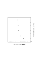
- Figure 18 is a graph showing the relationship between the dimensions of a contact hole and the impurity concentration in the semiconductor substrate directly below the contact hole.
- Figure 18 shows the results of a simulation of the impurity concentration in the region directly below the contact hole when ions are implanted under the same conditions into a semiconductor substrate through contact holes of the same depth and different widths.
- the larger the dimensions of the contact hole the higher the impurity concentration can be in the region directly below the contact hole. It can be considered that in a semiconductor substrate, the higher the impurity concentration, the higher the carrier concentration.
- the performance required for an IGBT is different from that required for a diode, so the optimal carrier concentration may differ between the IGBT region and the diode region.
- the carrier concentration of the contact region located in the IGBT region is desirable for the carrier concentration of the contact region located in the IGBT region to be higher than the carrier concentration of the contact region located in the diode region.
- the p-type carrier concentration of the first doped region 76 can be made higher than the p-type carrier concentration of the second doped region 78, thereby improving the turn-off performance of the IGBT 12A while reducing the switching loss of the diode 14A.
- the first doped region 76 and the second doped region 78 can be formed simultaneously by a single ion implantation. Therefore, according to the reverse conducting IGBT 10 of this embodiment, it is easy to control the carrier concentration to obtain the desired performance in both the IGBT 12A and the diode 14A.
- the reverse conducting IGBT 10 of the present embodiment has the following advantages.
- the multiple contact holes 38 include a first contact hole 46 provided in the IGBT region 12 and a second contact hole 48 provided in the diode region 14.
- the second region 54 includes a first doped region 76 exposed by the first contact hole 46 and a second doped region 78 exposed by the second contact hole 48.
- a dimension D1 of the first contact hole 46 in the first direction (X-axis direction) is larger than a dimension D2 of the second contact hole 48 in the first direction (X-axis direction), and a carrier concentration of the second conductivity type (p-type) of the first doped region 76 is higher than a carrier concentration of the second conductivity type (p-type) of the second doped region 78.
- the dimension D1 of the first contact hole 46 in the first direction may be the dimension of the bottom 46B of the first contact hole 46 that exposes the semiconductor substrate 16
- the dimension D2 of the second contact hole 48 in the first direction may be the dimension of the bottom 48B of the second contact hole 48 that exposes the semiconductor substrate 16.
- the first contact hole 46 and the second contact hole 48 have different dimensions at the bottoms 46B, 46B that expose the semiconductor substrate 16, so that the concentration of the impurities implanted into the first doped region 76 and the second doped region 78 can be effectively changed. This makes it easy to control the carrier concentration in the first doped region 76 and the second doped region 78.
- the dimension D1 of the first contact hole 46 in the first direction (X-axis direction) may be at least 1.2 times the dimension D2 of the second contact hole 48 in the first direction (X-axis direction). According to this configuration, by utilizing the difference in dimensions between the first contact hole 46 and the second contact hole 48, the concentration of the impurity implanted into the first doped region 76 of the IGBT region 12 can be made sufficiently higher than the concentration of the impurity implanted into the second doped region 78 of the diode region 14.
- the carrier concentration of the second conductivity type (p-type) of the first doped region 76 may be at least 5% higher than the carrier concentration of the second conductivity type (p-type) of the second doped region 78 . According to this configuration, it is possible to improve the performance of the IGBT 12A while reducing the switching loss of the diode 14A.
- Performing ion implantation includes simultaneously forming, in the second region 54, a first doped region 76 exposed through the first contact hole 46 and a second doped region 78 exposed through the second contact hole 48.
- the carrier concentration of the second conductivity type (p type) of the first doped region 76 is higher than the carrier concentration of the second conductivity type (p type) of the second doped region 78.
- This configuration allows the first doped region 76 and the second doped region 78, which have different carrier concentrations, to be formed simultaneously, making it possible to easily control the carrier concentration in the IGBT region 12 and the diode region 14 while preventing the manufacturing process from becoming too complicated.
- the above embodiment can be modified as follows.
- the pitch of the multiple trenches 32 does not have to be constant between the IGBT region 12 and the diode region 14 .
- the reverse conducting IGBT 200 differs from the reverse conducting IGBT 10 shown in FIGS. 3 and 4 in that the pitch of the multiple trenches 32 is different between the IGBT region 12 and the diode region 14.
- Fig. 19 is an enlarged plan view of the reverse conducting IGBT 200.
- Fig. 20 is a schematic cross-sectional view of the reverse conducting IGBT 200 taken along line F20-F20 shown in Fig. 19.
- the multiple trenches 32 may include a first multiple trenches 202 arranged in the IGBT region 12 and a second multiple trenches 204 arranged in the diode region 14.
- a pitch P T2 of the second multiple trenches 204 in the X-axis direction may be smaller than a pitch P T1 of the first multiple trenches 202 in the X-direction.
- the dimension D1 in the X-axis direction of the first contact hole 46 is also larger than the dimension D2 in the X-axis direction of the second contact hole 48.
- the p-type carrier concentration of the first doped region 76 can be made higher than the p-type carrier concentration of the second doped region 78.
- the pitch of the trenches 32 in the boundary region 30 may be the same as the pitch PT2 in the diode region 14. In another example, the pitch of the trenches 32 in the boundary region 30 may be the same as PT1 , or may be between PT2 and PT1 .
- the number of contact plugs 40 disposed between the two trenches 32 may be multiple.
- the dimension DT of the trench 32 in the X-axis direction may be the same or different in the IGBT region 12, the boundary region 30, and the diode region 14.
- a lifetime control region (not shown) for reducing switching loss may be formed in the diode region 14.
- the lifetime control region may be formed by irradiating the semiconductor substrate 16 with helium (He) ions.
- the lifetime control region may also be formed in the boundary region 30.
- the semiconductor substrate 16 may be a SiC substrate.
- a structure in which the conductivity type of each region in the semiconductor substrate 16 is inverted may be employed. That is, a p-type region may be an n-type region, and an n-type region may be a p-type region.
- a first layer is formed on a second layer is intended to mean that in some embodiments, the first layer may be placed directly on the second layer in contact with the second layer, while in other embodiments, the first layer may be placed above the second layer without contacting the second layer. In other words, the term “on” does not exclude a structure in which another layer is formed between the first and second layers.
- the Z-axis direction used in this disclosure does not necessarily have to be the vertical direction, nor does it have to completely coincide with the vertical direction. Therefore, various structures according to this disclosure (e.g., the structure shown in FIG. 1) are not limited to the "up” and “down” in the Z-axis direction described in this specification being "up” and “down” in the vertical direction.
- the X-axis direction may be the vertical direction
- the Y-axis direction may be the vertical direction.
- the plurality of contact plugs (40) are respectively embedded in a plurality of contact holes (38), and
- (Appendix 2) A reverse conducting IGBT as described in Appendix 1, wherein the first direction dimension (D 1 ) of the first contact hole (46) is the dimension of a bottom (46B) of the first contact hole (46) that exposes the semiconductor substrate (16), and the first direction dimension (D 2 ) of the second contact hole (48) is the dimension at a bottom (48B) of the second contact hole (48) that exposes the semiconductor substrate (16).
- the second region (54) is a base region (58) adjacent the first doped region (76); an anode region (60) adjacent said second doped region (78), 10.
- (Appendix 11) Further comprising a first electrode (20) formed on the insulating layer (18); The reverse conducting IGBT according to any one of appendices 1 to 10, wherein the first electrode (20) is electrically connected to the first doped region (76) via the contact plug (40) embedded in the first contact hole (46), and is electrically connected to the second doped region (78) via the contact plug (40) embedded in the second contact hole (48).
Landscapes
- Electrodes Of Semiconductors (AREA)
Priority Applications (1)
| Application Number | Priority Date | Filing Date | Title |
|---|---|---|---|
| JP2025505130A JPWO2024185360A1 (https=) | 2023-03-06 | 2024-02-05 |
Applications Claiming Priority (2)
| Application Number | Priority Date | Filing Date | Title |
|---|---|---|---|
| JP2023-033611 | 2023-03-06 | ||
| JP2023033611 | 2023-03-06 |
Publications (1)
| Publication Number | Publication Date |
|---|---|
| WO2024185360A1 true WO2024185360A1 (ja) | 2024-09-12 |
Family
ID=92674402
Family Applications (1)
| Application Number | Title | Priority Date | Filing Date |
|---|---|---|---|
| PCT/JP2024/003624 Ceased WO2024185360A1 (ja) | 2023-03-06 | 2024-02-05 | 逆導通igbtおよび逆導通igbtの製造方法 |
Country Status (2)
| Country | Link |
|---|---|
| JP (1) | JPWO2024185360A1 (https=) |
| WO (1) | WO2024185360A1 (https=) |
Citations (5)
| Publication number | Priority date | Publication date | Assignee | Title |
|---|---|---|---|---|
| WO2012169053A1 (ja) * | 2011-06-09 | 2012-12-13 | トヨタ自動車株式会社 | 半導体装置および半導体装置の製造方法 |
| WO2014054319A1 (ja) * | 2012-10-02 | 2014-04-10 | 三菱電機株式会社 | 半導体装置およびその製造方法 |
| JP2014192278A (ja) * | 2013-03-27 | 2014-10-06 | New Japan Radio Co Ltd | 半導体装置の製造方法 |
| WO2018052099A1 (ja) * | 2016-09-14 | 2018-03-22 | 富士電機株式会社 | Rc-igbtおよびその製造方法 |
| JP2021077813A (ja) * | 2019-11-12 | 2021-05-20 | 株式会社デンソー | 半導体装置 |
-
2024
- 2024-02-05 WO PCT/JP2024/003624 patent/WO2024185360A1/ja not_active Ceased
- 2024-02-05 JP JP2025505130A patent/JPWO2024185360A1/ja active Pending
Patent Citations (5)
| Publication number | Priority date | Publication date | Assignee | Title |
|---|---|---|---|---|
| WO2012169053A1 (ja) * | 2011-06-09 | 2012-12-13 | トヨタ自動車株式会社 | 半導体装置および半導体装置の製造方法 |
| WO2014054319A1 (ja) * | 2012-10-02 | 2014-04-10 | 三菱電機株式会社 | 半導体装置およびその製造方法 |
| JP2014192278A (ja) * | 2013-03-27 | 2014-10-06 | New Japan Radio Co Ltd | 半導体装置の製造方法 |
| WO2018052099A1 (ja) * | 2016-09-14 | 2018-03-22 | 富士電機株式会社 | Rc-igbtおよびその製造方法 |
| JP2021077813A (ja) * | 2019-11-12 | 2021-05-20 | 株式会社デンソー | 半導体装置 |
Also Published As
| Publication number | Publication date |
|---|---|
| JPWO2024185360A1 (https=) | 2024-09-12 |
Similar Documents
| Publication | Publication Date | Title |
|---|---|---|
| US12419067B2 (en) | Semiconductor device | |
| US9576841B2 (en) | Semiconductor device and manufacturing method | |
| CN114068695B (zh) | 半导体装置 | |
| US8212314B2 (en) | Semiconductor device and method for manufacturing the same | |
| US20020008237A1 (en) | Schottky diode having increased forward current with improved reverse bias characteristics and method of fabrication | |
| US6818940B2 (en) | Insulated gate bipolar transistor having trench gates of rectangular upper surfaces with different widths | |
| JP7528687B2 (ja) | 半導体装置 | |
| WO2016199546A1 (ja) | 電力用半導体装置 | |
| JP2021034444A (ja) | 半導体装置 | |
| CN114566536B (zh) | 半导体装置及半导体装置的制造方法 | |
| JP7607538B2 (ja) | 半導体装置 | |
| JP2023550855A (ja) | 半導体構造及びその製造方法 | |
| JP2023158315A (ja) | 半導体装置 | |
| US20240088221A1 (en) | Semiconductor device | |
| WO2024185360A1 (ja) | 逆導通igbtおよび逆導通igbtの製造方法 | |
| KR20260044950A (ko) | 반도체 정류기 디바이스 및 이를 위한 제조 방법 | |
| US20250120168A1 (en) | Semiconductor device | |
| US20260020326A1 (en) | Semiconductor device and method of manufacturing semiconductor device | |
| JP7294097B2 (ja) | 半導体装置の製造方法 | |
| US20240405108A1 (en) | Semiconductor device and method of manufacturing semiconductor device | |
| JP7123258B2 (ja) | 半導体装置、および、半導体装置の製造方法 | |
| WO2026014345A1 (ja) | 半導体装置 | |
| WO2025239027A1 (ja) | 半導体装置 | |
| JP2026013567A (ja) | 半導体装置 | |
| JP2025098432A (ja) | 半導体装置および半導体装置の製造方法 |
Legal Events
| Date | Code | Title | Description |
|---|---|---|---|
| 121 | Ep: the epo has been informed by wipo that ep was designated in this application |
Ref document number: 24766735 Country of ref document: EP Kind code of ref document: A1 |
|
| WWE | Wipo information: entry into national phase |
Ref document number: 2025505130 Country of ref document: JP |
|
| NENP | Non-entry into the national phase |
Ref country code: DE |
|
| 122 | Ep: pct application non-entry in european phase |
Ref document number: 24766735 Country of ref document: EP Kind code of ref document: A1 |