WO2024177013A1 - 半導体パッケージ、及びモジュール - Google Patents
半導体パッケージ、及びモジュール Download PDFInfo
- Publication number
- WO2024177013A1 WO2024177013A1 PCT/JP2024/005799 JP2024005799W WO2024177013A1 WO 2024177013 A1 WO2024177013 A1 WO 2024177013A1 JP 2024005799 W JP2024005799 W JP 2024005799W WO 2024177013 A1 WO2024177013 A1 WO 2024177013A1
- Authority
- WO
- WIPO (PCT)
- Prior art keywords
- lead frame
- semiconductor package
- substrate
- groove
- sealing portion
- Prior art date
- Legal status (The legal status is an assumption and is not a legal conclusion. Google has not performed a legal analysis and makes no representation as to the accuracy of the status listed.)
- Ceased
Links
Images










Classifications
-
- H—ELECTRICITY
- H10—SEMICONDUCTOR DEVICES; ELECTRIC SOLID-STATE DEVICES NOT OTHERWISE PROVIDED FOR
- H10W—GENERIC PACKAGES, INTERCONNECTIONS, CONNECTORS OR OTHER CONSTRUCTIONAL DETAILS OF DEVICES COVERED BY CLASS H10
- H10W72/00—Interconnections or connectors in packages
-
- H—ELECTRICITY
- H10—SEMICONDUCTOR DEVICES; ELECTRIC SOLID-STATE DEVICES NOT OTHERWISE PROVIDED FOR
- H10W—GENERIC PACKAGES, INTERCONNECTIONS, CONNECTORS OR OTHER CONSTRUCTIONAL DETAILS OF DEVICES COVERED BY CLASS H10
- H10W74/00—Encapsulations, e.g. protective coatings
-
- H—ELECTRICITY
- H10—SEMICONDUCTOR DEVICES; ELECTRIC SOLID-STATE DEVICES NOT OTHERWISE PROVIDED FOR
- H10W—GENERIC PACKAGES, INTERCONNECTIONS, CONNECTORS OR OTHER CONSTRUCTIONAL DETAILS OF DEVICES COVERED BY CLASS H10
- H10W74/00—Encapsulations, e.g. protective coatings
- H10W74/10—Encapsulations, e.g. protective coatings characterised by their shape or disposition
-
- H—ELECTRICITY
- H10—SEMICONDUCTOR DEVICES; ELECTRIC SOLID-STATE DEVICES NOT OTHERWISE PROVIDED FOR
- H10W—GENERIC PACKAGES, INTERCONNECTIONS, CONNECTORS OR OTHER CONSTRUCTIONAL DETAILS OF DEVICES COVERED BY CLASS H10
- H10W74/00—Encapsulations, e.g. protective coatings
- H10W74/40—Encapsulations, e.g. protective coatings characterised by their materials
-
- H—ELECTRICITY
- H10—SEMICONDUCTOR DEVICES; ELECTRIC SOLID-STATE DEVICES NOT OTHERWISE PROVIDED FOR
- H10W—GENERIC PACKAGES, INTERCONNECTIONS, CONNECTORS OR OTHER CONSTRUCTIONAL DETAILS OF DEVICES COVERED BY CLASS H10
- H10W90/00—Package configurations
Definitions
- the present invention relates to a semiconductor package.
- Patent Document 1 discloses a current sensor that has a lead terminal, a conductor through which a current to be measured flows, a magnetoelectric conversion element that outputs a signal whose magnitude is proportional to the magnetic field generated by the current flowing through the conductor, a signal processing IC that processes the signal, and another lead terminal that outputs a signal from the signal processing IC, and is a semiconductor package in which the conductor, magnetoelectric conversion element, and signal processing IC are sealed with molded resin.
- Patent Document 1 Japanese Patent No. 6321800
- a semiconductor package may include a first lead frame, an element that outputs a signal corresponding to a current flowing through the first lead frame, a second lead frame that is electrically insulated from the first lead frame and outputs a signal corresponding to the signal from the element, and a sealing portion that seals the element, a portion of the first lead frame, and a portion of the second lead frame with resin.
- a terminal portion of the first lead frame may be exposed from a first surface of the sealing portion.
- a terminal portion of the second lead frame may be exposed from a second surface that faces the first surface of the sealing portion in a first direction.
- the sealing portion may have at least one groove extending in a second direction intersecting the first direction on at least one surface other than the first surface and the second surface.
- the sealing portion may include a third surface and a fourth surface that face each other in the thickness direction, and a fifth surface and a sixth surface that face each other in the second direction that intersects with each of the first direction and the thickness direction.
- the at least one groove may include a first groove that extends from the fifth surface toward the sixth surface in each of the third surface and the fourth surface.
- the first groove may extend along the second direction.
- the at least one groove may include a second groove extending from the third surface toward the fourth surface on each of the fifth surface and the sixth surface.
- the second groove may extend along the thickness direction.
- the first groove may be in communication with the second groove.
- the sealing portion may include a third surface and a fourth surface that face each other in the thickness direction, and a fifth surface and a sixth surface that face each other in the second direction that intersects with each of the first direction and the thickness direction.
- the at least one groove may include a groove that is continuous around the third surface, the fourth surface, the fifth surface, and the sixth surface.
- the recess width of at least one of the grooves may be 1 mm or more.
- the depth of at least one of the grooves may be 0.5 mm or more.
- the sealing portion may include a plurality of grooves as the at least one groove, and the spacing between at least one of the plurality of grooves may be wider than the spacing between other grooves of the plurality of grooves other than the at least one groove.
- the sealing portion may include a plurality of grooves as the at least one groove, and the spacing between the grooves in a central portion of the plurality of grooves in the first direction may be wider than the spacing between the grooves other than the grooves in the central portion.
- the terminal portion of the first lead frame may be electrically connected to a first power supply system, and the terminal portion of the second lead frame may be connected to a second power supply system that applies a lower voltage than the first power supply system.
- the installation surfaces of the terminal portion of the first lead frame and the terminal portion of the second lead frame may be located outside the thickness direction relative to the third surface or the fourth surface when viewed from the second direction.
- the side of at least one of the grooves may be inclined so as to widen from the bottom surface toward the opening when viewed from the second direction.
- the inclination angle of the side surface of at least one of the grooves may be 85 degrees or less with respect to the bottom surface.
- the protruding side of at least one of the grooves may be chamfered or rounded to 0.1 mm or more.
- the sealing portion may seal the element, a portion of the first lead frame, and a portion of the second lead frame with a molding resin.
- the element may be at least one magnetoelectric conversion element that outputs a signal according to the magnitude of a magnetic field generated by a current flowing through the first lead frame.
- any of the semiconductor packages may further include a signal processing IC that processes the signal output from the at least one magnetoelectric conversion element and outputs the processed signal via the second lead frame.
- the sealing portion may further seal the signal processing IC.
- the at least one magnetoelectric conversion element and the signal processing IC may be electrically connected via a first wire.
- the signal processing IC and the second lead frame may be electrically connected via a second wire.
- the at least one groove may be provided in a position that does not overlap the first wire and the second wire in a plan view.
- the terminal portion of the first lead frame may extend linearly from the first surface in the first direction, and the terminal portion of the second lead frame may extend linearly from the second surface in the first direction.
- the terminal portion of the first lead frame may have a through hole for screwing the semiconductor package to a substrate on which the semiconductor package is mounted using a bolt.
- a module according to one aspect of the present invention may include any one of the semiconductor packages and a substrate on which the semiconductor package is mounted.
- the substrate may include a slit having at least a portion that is aligned along the second direction at a position that overlaps the sealing portion when viewed in the thickness direction of the sealing portion.
- the slit may have a continuous portion that intersects with a fifth surface and a sixth surface that face each other in the second direction of the sealing portion when viewed in the thickness direction of the sealing portion.
- the substrate may have a first land electrically connected to the first lead frame.
- the substrate may have a second land electrically connected to the second lead frame.
- the slit may be disposed between the first land and the second land.
- the width of the slit in the second direction may be greater than the sum of the widths of the first land and the second land in the second direction.
- the width of the slit may be 1 mm or more.
- the sealing portion may include a third surface and a fourth surface that face each other in the thickness direction, and a fifth surface and a sixth surface that face each other in the second direction that intersects with each of the first direction and the thickness direction.
- the at least one groove may include a first groove that extends from the fifth surface toward the sixth surface in each of the third surface and the fourth surface.
- the fourth surface may face the substrate.
- the fourth surface of the sealing portion may be located at a higher position relative to the substrate than the respective mounting surfaces of the terminal portion of the first lead frame and the terminal portion of the second lead frame.
- the terminal portion of the first lead frame may have a first portion that bends from the first surface toward the substrate in the thickness direction, and a second portion that is thinner than the first portion and extends from the first portion further in the thickness direction through a hole in the substrate.
- the terminal portion of the second lead frame may have a third portion that bends from the second surface toward the substrate in the thickness direction, and a fourth portion that is thinner than the third portion and extends from the third portion further in the thickness direction through a hole in the substrate.
- the diameter of the hole through which the second portion of the substrate passes may be narrower than the width of the first portion
- the diameter of the hole through which the fourth portion of the substrate passes may be narrower than the width of the third portion.
- the width of the slit in the first direction and the second direction may be greater than the width of the sealing portion in the first direction and the second direction, and a portion of the sealing portion may be disposed within the slit.
- the terminal portion of the first lead frame may extend linearly from the first surface in the first direction, and the terminal portion of the second lead frame may extend linearly from the second surface in the first direction.
- the terminal portion of the first lead frame may have a first portion that bends from the first surface in the thickness direction away from the bottom surface of the sealing portion, or in a diagonal direction between the thickness direction and the first direction, when viewed from the second direction, and a second portion that bends from the first portion in the first direction, and the second portion may have an installation surface for the substrate.
- the terminal portion of the second lead frame may have a third portion that bends from the second surface in the thickness direction away from the bottom surface of the sealing portion, or in a diagonal direction between the thickness direction and the first direction, when viewed from the second direction, and a fourth portion that bends from the third portion in the first direction, and the fourth portion may have an installation surface for the substrate.
- the terminal portion of the first lead frame may have a through hole for screwing the semiconductor package to a substrate on which the semiconductor package is mounted via a bolt.
- the terminal portion of the first lead frame may be disposed on a mounting surface of the substrate, and the substrate may have a land on a surface opposite the mounting surface for electrically connecting the first lead frame to a power supply system that applies a voltage to the first lead frame, and the terminal portion of the first lead frame and the land may be electrically connected via the bolt.
- FIG. 2 is a schematic plan view of the current sensor according to the first embodiment as viewed from the ceiling surface side (Z-axis direction).
- FIG. 1B is a schematic plan view of the current sensor shown in FIG. 1A as viewed from the side (X-axis direction).
- FIG. 13 is a diagram for explaining a spatial distance.
- FIG. 13 is a diagram for explaining a creepage distance.
- FIG. 13 is a diagram for explaining a comparative example.
- 1 is a schematic plan view of a current sensor according to a first embodiment mounted on a substrate, as viewed from the ceiling surface side (Z-axis direction) of the current sensor.
- FIG. 4B is a schematic plan view of the current sensor shown in FIG.
- FIG. 5B is a schematic plan view of the current sensor shown in FIG. 5A as viewed from the side (X-axis direction).
- FIG. 5B is a schematic plan view of the current sensor 10 shown in FIG. 5A as viewed from the side (Y-axis direction).
- 13 is a schematic plan view of a current sensor according to a third embodiment, as viewed from the ceiling surface side (Z-axis direction).
- FIG. 6B is a schematic plan view of the current sensor shown in FIG.
- FIG. 6A is viewed from the side (X-axis direction).
- 13 is a schematic plan view of the current sensor according to the third embodiment, when viewed from the ceiling surface side (Z-axis direction) of the current sensor, in a state where the current sensor is mounted on a substrate.
- FIG. 7B is a schematic plan view of the current sensor shown in FIG. 7A mounted on a substrate, as viewed from the side (X-axis direction) of the current sensor.
- 13 is a schematic plan view of a current sensor according to a fourth embodiment, as viewed from the ceiling surface side (Z-axis direction).
- FIG. 8B is a schematic plan view of the current sensor shown in FIG. 8A as viewed from the side (X-axis direction).
- FIG. 13 is a schematic plan view of the current sensor according to the fourth embodiment, as viewed from the side (X-axis direction) of the current sensor mounted on a substrate.
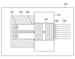
- FIG. 13 is a schematic plan view of the current sensor mounted on a substrate according to the fifth embodiment, as viewed from the ceiling surface side (Z-axis direction).
- FIG. 10B is a schematic plan view of the current sensor mounted on the substrate shown in FIG. 10A as viewed from the side (X-axis direction).
- FIG. 11 is a schematic plan view of a current sensor according to another embodiment, as viewed from the ceiling surface side (Z-axis direction).
- 13 is a schematic cross-sectional view of a current sensor according to another embodiment, as viewed from the side (X-axis direction).
- FIG. 1A and 1B are schematic diagrams of a semiconductor package that functions as a current sensor 10 according to the first embodiment.
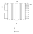
- FIG. 1A is a schematic plan view of the current sensor 10 according to the first embodiment as viewed from the ceiling surface side (Z-axis direction).
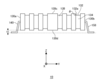
- FIG. 1B is a schematic plan view of the current sensor 10 shown in FIG. 1A as viewed from the side surface side (X-axis direction).
- the coordinate system is defined as the X-axis direction parallel to the paper from bottom to top, the Y-axis direction parallel to the paper from left to right, and the Z-axis direction perpendicular to the paper from back to front.
- the Y-axis direction is an example of a first direction.
- the X-axis direction is an example of a second direction.
- the Z-axis direction is an example of a thickness direction.
- the first direction is the direction from surface 130a, on which the pair of lead terminals 140a are exposed, to surface 130b, which faces surface 130a and on which the multiple lead terminals 150a are exposed, of the side surfaces of the sealing portion 130.
- the second direction is the direction from surface 130f, on which the pair of lead terminals 140a and the multiple lead terminals 150a are not exposed, to surface 130e, which faces surface 130f.
- the thickness direction is the direction from surface 130d on the bottom side of the sealing portion 130 to surface 130c on the ceiling side of the sealing portion 130.
- the first direction is a direction along the substrate when the current sensor 10 is mounted on the substrate, and is a direction from surface 130a, on which the pair of lead terminals 140a are exposed, toward surface 130b, which faces surface 130a and on which the multiple lead terminals 150a are exposed.
- the second direction is a direction along the substrate when the current sensor 10 is mounted on the substrate, and is a direction that intersects with the first direction.
- the thickness direction is a direction that penetrates the substrate when the current sensor 10 is mounted on the substrate, or more specifically, a direction perpendicular to the substrate.
- the current sensor 10 includes a signal processing IC 100, a magnetoelectric conversion element 20, a magnetoelectric conversion element 22, a sealing portion 130, a lead frame 140, and a lead frame 150.
- the magnetoelectric conversion element 20 and the magnetoelectric conversion element 22 are electrically connected to the signal processing IC 100 via a wire 30.
- the signal processing IC 100 is electrically connected to the lead frame 150 via a wire 108.
- the wire 30 is an example of a first wire
- the wire 108 is an example of a second wire.
- the lead frame 140 includes a pair of lead terminals 140a exposed from the surface 130a of the sealing portion 130, and a conductor 140b sealed in the sealing portion 130 and arranged to surround at least a portion of the magnetoelectric conversion element 20 and the magnetoelectric conversion element 22.
- the lead frame 150 includes a plurality of lead terminals 150a exposed from the surface 130b facing the surface 130a of the sealing portion 130 in the Y-axis direction, and a conductor 150b electrically connected to the signal processing IC 100 via the wire 108.
- the shapes of the lead frame 140 and the lead frame 150 shown in FIG. 1A are merely examples, and the shapes of the lead frame 140 and the lead frame 150 may be any shape.
- Lead frame 140 is a primary side lead frame, and lead frame 150 is a secondary side lead frame. Lead frame 140 is physically separate from lead frame 150 and electrically insulated from it. Lead frame 140 is an example of a first lead frame, and lead frame 150 is an example of a second lead frame. Lead terminal 140a is electrically connected to a high voltage power supply system. Lead terminal 150a is electrically connected to a low voltage power supply system that applies a lower voltage than the high voltage power supply system.
- the high voltage power supply system is an example of a first power supply system.
- the low voltage power supply system is an example of a second power supply system.
- the sealing section 130 seals the magnetoelectric conversion element 20, the magnetoelectric conversion element 22, the conductor 140b, the conductor 150b, the signal processing IC 100, the wire 30, and the wire 108 with a molded resin.
- the sealing section 130 may be formed by compression molding or transfer molding using a mold.
- the molded resin may be, for example, an epoxy-based thermosetting resin with silica added.
- the molded resin may be a thermoplastic resin such as a liquid crystal polymer.
- the magnetoelectric conversion elements 20 and 22 detect a magnetic field in a specific direction that changes according to the measurement current flowing through the conductor 140b, and the signal processing IC 100 amplifies a signal according to the magnitude of the magnetic field and outputs the amplified signal through the lead frame 150.
- the magnetoelectric conversion elements 20 and 22 are an example of an element that outputs a signal according to the current flowing through the lead frame 140.
- the semiconductor package may be, for example, a photocoupler. If the semiconductor package is a photocoupler, the element may be an LED element that outputs light as a signal according to the current flowing through the lead frame 140. In this case, the semiconductor package may further incorporate a light receiving element that receives the light output by the LED element in the sealing portion 130.
- the magnetoelectric conversion elements 20 and 22 are made of compound semiconductors formed on a GaAs substrate, and are chips cut into a square or rectangular shape when viewed in a plan view from the Z-axis direction.
- the magnetoelectric conversion elements 20 and 22 When detecting a magnetic field in the Z-axis direction, the magnetoelectric conversion elements 20 and 22 may be Hall elements. When detecting a magnetic field in one axis direction on the XY plane, the magnetoelectric conversion elements 20 and 22 may be magnetoresistance elements or fluxgate elements.
- the signal processing IC 100 is a large-scale integrated circuit (LSI).
- the signal processing IC 100 is a signal processing circuit and a bias circuit made of a Si monolithic semiconductor formed on a Si substrate.
- the bias circuit applies a corrected drive current or drive voltage to the magnetoelectric conversion elements 20 and 22.
- the signal processing circuit processes an output signal according to the magnitude of the magnetic field output from the magnetoelectric conversion elements 20 and 22.
- the signal processing circuit corrects the measurement current flowing through the lead frame 140 based on the output signal, and outputs an output signal indicating an accurate current value via the lead terminal 150a.
- the signal processing circuit reduces noise components contained in the output signal of the magnetoelectric conversion element 20 and the output signal of the magnetoelectric conversion element 22 based on the difference between the output signal of the magnetoelectric conversion element 20 and the output signal of the magnetoelectric conversion element 22, amplifies the output signal of the magnetoelectric conversion element 20 and the output signal of the magnetoelectric conversion element 22 with the noise components reduced, calculates the current value of the measurement current based on the amplified output signal, and outputs an output signal indicating the current value.
- the current sensor 10 may include at least one magnetoelectric conversion element.
- the current sensor 10 configured in this manner, it is necessary to ensure insulation between the primary lead terminal 140a and the secondary lead terminal 150a.
- an insulator such as molded resin and ensure both spatial distance and creepage distance.
- spatial distance k1 indicates the shortest distance through space between two conductive parts (terminal parts).
- creepage distances k2 and k3 indicate the shortest distance along the surface of the insulator between two conductive parts.
- a semiconductor package such as a current sensor 10 is provided that can more reliably ensure insulation while preventing the size of the sealing portion 130 from increasing relative to the required creepage distance.
- the sealing unit 130 is a structure having six faces, such as a rectangular parallelepiped or cube. In addition to faces 130a and 130b that face each other in the Y-axis direction, the sealing unit 130 has faces 130c and 130d that face each other in the thickness direction (Z-axis direction), and faces 130e and 130f that face each other in the X-axis direction.
- the sealing portion 130 may have at least one groove extending in the X-direction or Z-direction on at least one of the faces 130c to 130f to ensure the spatial distance and creepage distance between the primary side lead terminal 140a and the secondary side lead terminal 150a.
- the sealing portion 130 includes a groove 132 extending from the surface 130e toward the surface 130f on each of the surfaces 130c and 130d.
- the surface 130c is the ceiling surface of the sealing portion 130
- the surface 130d is the bottom surface of the sealing portion 130.
- the ceiling surface of the sealing portion 130 may be the surface on the same side as the sensing surfaces of the magnetoelectric conversion elements 20 and 22, and the bottom surface of the sealing portion 130 may be the surface opposite to the sensing surfaces of the magnetoelectric conversion elements 20 and 22.
- the sealing portion 130 may include a plurality of grooves 132.
- the grooves 132 may be provided on each of the surfaces 130c and 130d along the X direction.
- the grooves 132 may be parallel to the X direction or may not be parallel to the X direction.
- the grooves 132 are an example of a first groove.
- the sealing portion 130 includes a groove 134 extending from the surface 130c toward the surface 130d on each of the surfaces 130e and 130f.
- the sealing portion 130 may include a plurality of grooves 134.
- Each of the plurality of grooves 132 is in communication with each of the plurality of grooves 134.
- the grooves 134 may be provided on each of the surfaces 130e and 130f along the Z direction.
- the grooves 134 may or may not be parallel to the Z direction.
- the grooves 134 are an example of a second groove.
- the creepage distance between primary side lead terminal 140a and secondary side lead terminal 150a can be made longer than when grooves 132 and 134 are not present. Therefore, even if the width in the Y direction and the height in the Z direction of sealing portion 130 are relatively short, the creepage distance required to ensure insulation between primary side lead terminal 140a and secondary side lead terminal 150a can be ensured.
- the recess width of grooves 132 and 134 may be 1 mm or more.
- the depth of the groove 132 and the groove 134 may be 0.5 mm or more. Furthermore, the interval W2 of at least one of the multiple grooves 132 and 134 in the Y-axis direction may be wider than the interval W3 of the other grooves other than the at least one groove. This allows a marking space for indicating characters or the like to be secured on the surface of the sealing portion 130. Furthermore, when mounting the current sensor 10 on the board 200, the current sensor 10 can be easily picked up by adsorption. Furthermore, by making the width of the central portion of the sealing portion 130 wider, the center of gravity can be positioned at the center of the sealing portion 130, and the current sensor 10 can be stabilized and mounted on the board 200.
- the magnetoelectric conversion elements 20 and 22 may be disposed between the grooves 132 and 132 without overlapping with the groove 132 in a plan view seen from the ceiling surface side. Alternatively, the magnetoelectric conversion elements 20 and 22 may be disposed so as to fit within the groove 132 in a plan view seen from the ceiling surface side. That is, the thickness of the sealing portion 130 facing the sensing surfaces of the magnetoelectric conversion elements 20 and 22 can be the same.
- the current sensor 10 is mounted on a substrate.
- the surface 130d of the sealing portion 130 that faces the substrate must be separated from the substrate. Therefore, the mounting surfaces of the lead terminals 140a and 150a may be located outside the surface 130d in the thickness direction (Z-axis direction) when viewed from the X-axis direction.
- the bottom surface of the surface 130d of the sealing portion 130 is located higher than the mounting surfaces of the lead terminals 140a and 150a with respect to the substrate. It is preferable that the distance h1 between the bottom surface of the surface 130d of the sealing portion 130 and the substrate is 1 mm or more.
- the surface 132a of the groove 132 may be inclined so as to widen from the bottom surface toward the opening when viewed from the X-axis direction.
- the side surface 134a of the groove 134 may be inclined so as to widen from the bottom surface toward the opening when viewed from the Z-axis direction.
- the inclination angle ⁇ of the surfaces 132a and 134a of the grooves 132 and 134 with respect to the bottom surface may be 85 degrees or less.
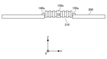
- FIG. 4A is a schematic plan view of the current sensor 10 according to the first embodiment mounted on the substrate 200, as viewed from the ceiling surface side (Z-axis direction) of the current sensor 10.
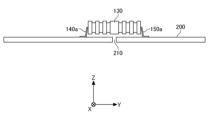
- FIG. 4B is a schematic plan view of the current sensor 10 shown in FIG. 4A mounted on the substrate 200, as viewed from the side side (X-axis direction) of the current sensor 10.
- the substrate 200 has a primary side land 202 on which the primary side lead terminal 140a is installed and electrically connected, and a secondary side land 204 on which the secondary side lead terminal 150a is installed and electrically connected.
- the lands 202 and 204 are made of a conductive material such as metal.
- the substrate 200 has a slit 210 at a position overlapping the sealing portion 130 when viewed from the Z-axis direction.
- the substrate 200 may have a slit 210 having at least a portion along the X-axis direction, between the land 202 and the land 204, at a position facing the surface 130d of the sealing portion 130.
- the slit 210 may have a main portion 210a extending in the X-axis direction and an extension portion 210b extending from both ends of the main portion 210a in the Y-axis direction toward the land 202, and the slit 210 may be U-shaped.
- the length of the main portion 210a in the X-axis direction is longer than the total width of the land 202 in the X-axis direction. Furthermore, the width of the main portion 210a in the Y-axis direction and the width of the extension portion 210b in the X-axis direction are 1 mm or more.
- the slit 210 has a continuous portion that intersects with the faces 130e and 130f when viewed from the ceiling surface side (Z-axis direction) of the sealing portion 130.
- the length of the slit 210 in the X-axis direction is longer than the width of the sealing portion 130 in the X-axis direction.
- the length of the slit 210 in the X-axis direction is longer than the total width of the lands 202 in the X-axis direction.
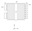
- FIG. 5A is a schematic plan view of the current sensor 10 according to the second embodiment as viewed from the ceiling surface side (Z-axis direction).
- FIG. 5B is a schematic plan view of the current sensor 10 shown in FIG. 5A as viewed from the side surface side (X-axis direction).
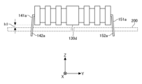
- FIG. 5C is a schematic plan view of the current sensor 10 shown in FIG. 5A as viewed from the side surface side (Y-axis direction).
- the lead terminal 140a has a wide portion 141a that bends from the surface 130a of the sealing portion 130 in the Z-axis direction toward the substrate, and a narrow portion 142a that is narrower in the X-axis direction than the wide portion 141a and extends from the wide portion 141a in the Z-axis direction through the hole 131 of the substrate 200.
- the terminal portion 150a has a wide portion 151a that bends from the surface 130b in the Z-axis direction toward the substrate 200, and a narrow portion 152a that is narrower than the wide portion and extends from the wide portion 151a in the Z-axis direction through the hole of the substrate 200.
- the diameter of the hole for the lead terminal 140a in the substrate 200 is narrower than the width of the wide portion 141a, and the diameter of the hole for the lead terminal 150a in the substrate 200 is narrower than the width of the wide portion 151a.
- the current sensor 10 according to the second embodiment differs from the current sensor 10 according to the first embodiment, in that the lead terminals 140a and 150a are dual in-line package (DIP) type semiconductor packages.
- DIP dual in-line package
- the wide portion 141a and the wide portion 151a extend outward in the Z-axis direction from the surface 130d of the sealing portion 130, and reach the substrate 200. This leaves a gap of distance h1 between the surface 130d of the sealing portion 130 and the mounting surface of the substrate 200 on the side of the current sensor 10. This ensures better insulation when the current sensor 10 is mounted on the substrate 200.
- FIG. 6A is a schematic plan view of the current sensor 10 according to the third embodiment, as viewed from the ceiling surface side (Z-axis direction).
- FIG. 6B is a schematic plan view of the current sensor 10 shown in FIG. 6A, as viewed from the side surface side (X-axis direction).
- FIG. 7A is a schematic plan view of the current sensor 10 according to the third embodiment, as viewed from the ceiling surface side (Z-axis direction) of the current sensor 10, mounted on the substrate 200.
- FIG. 7B is a schematic plan view of the current sensor 10 shown in FIG. 7A, as viewed from the side surface side (X-axis direction) of the current sensor 10, mounted on the substrate 200.
- the current sensor 10 according to the third embodiment differs from the current sensor 10 according to the first and second embodiments in that the lead terminal 140a of the lead frame 140 extends linearly in the Y-axis direction from the surface 130a, and the lead terminal 150a of the lead frame 150 extends linearly in the Y-axis direction from the surface 130b. Furthermore, in the substrate 200 on which the current sensor 10 according to the third embodiment is mounted, the widths of the slit 210 in the X-axis direction and the Y-axis direction are longer than the widths of the sealing portion 130 in the X-axis direction and the Y-axis direction. A part of the sealing portion 130 is disposed within the slit 210. This ensures better insulation when the current sensor 10 is mounted on the substrate 200. Furthermore, the thickness in the Z-axis direction can be reduced when the current sensor 10 is mounted on the substrate 200.
- the lead terminals 140a and 150a are not formed but extend linearly, the lead length to the soldering position where they are electrically connected to the substrate 200 can be shortened, and heat generation in the lead terminals 140a and 150a can be suppressed.
- the lead terminal 140a can be made thicker to withstand large currents without the need for forming, making it easier to process the lead frame.
- the contact area between the lead terminal 140a and the land 202 of the substrate 200 can be increased, and the contact resistance between the lead terminal 140a and the land 202 of the substrate 200 can be reduced.
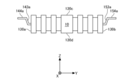
- FIG. 8A is a schematic plan view of the current sensor 10 according to the fourth embodiment, as viewed from the ceiling surface side (Z-axis direction).
- FIG. 8B is a schematic plan view of the current sensor 10 shown in FIG. 8A, as viewed from the side side (X-axis direction).
- FIG. 9 is a schematic plan view of the current sensor 10 according to the fourth embodiment, as viewed from the side side (X-axis direction) of the current sensor 10, when mounted on a substrate 200.
- the lead terminal 140a has a portion 143a that bends from the surface 130a of the sealing portion 130 in a diagonal direction between the Z-axis direction and the Y-axis direction so as to move away from the surface 130d, as viewed from the X-axis direction, and a portion 144a that bends further in the Y-axis direction from the portion 143a.
- the portion 144a has an installation surface for the substrate 200.
- the portion 143a extends from the surface 130a in the Y-axis direction, and may be bent perpendicularly to the Z-axis direction so as not to come into contact with the surface 130a so as to move away from the surface 130d.
- lead terminal 150a When viewed from the X-axis direction, lead terminal 150a has a portion 153a that bends from surface 130b of sealing portion 130 in a diagonal direction between the Z-axis direction and the Y-axis direction so as to move away from surface 130d, and a portion 154a that bends further in the Y-axis direction from portion 153a.
- Portion 154a has an installation surface for mounting to substrate 200.
- Portion 153a extends from surface 130a in the Y-axis direction, and may be further bent perpendicular to the Z-axis direction so as not to come into contact with surface 130a so as to move away from surface 130d.
- the lead terminal 140a of the lead frame 140 extends linearly in the Y-axis direction from the surface 130a, and the lead terminal 150a of the lead frame 150 extends linearly in the Y-axis direction from the surface 130b.
- the lead terminal 140a has a hole 148a for inserting the bolt 160.
- the substrate 200 also has a hole 205 for inserting the bolt 160.
- the hole 148a may be a through hole or a U-shaped groove.
- the hole 148a may be countersunk.
- the substrate 200 further has lands 203 on its back surface opposite the mounting surface on which the lands 202 are installed, for electrically connecting to a power supply system that applies voltage to the lead frame 140.
- the lead terminals 140a of the lead frame 140 and the lands 203 on the back surface of the substrate 200 are electrically connected via bolts 160.
- the substrate 200 may be equipped with an inverter module 170 on its back surface to which current is supplied to the lead frame 140.
- the current from the inverter module 170 may be supplied to a motor or the like that serves as a drive source for the vehicle.
- the lead terminal 140a can be electrically connected directly to the inverter module 170 via a bolt 160 inserted into a hole 148a provided at the tip of the lead terminal 140a. This makes it possible to eliminate the need for a copper foil pattern for electrically connecting the inverter module 170 and the lead terminal 140a.
- the land 202 on the mounting surface of the substrate 200 does not have to be provided, but the presence of the land 202 allows the lead terminal 140a to be fixed to the substrate 200 by soldering. Furthermore, the presence of the land 202 can improve the heat dissipation effect.
- FIG. 11 is a schematic plan view of a current sensor 10 according to another embodiment, as viewed from the ceiling surface side (Z-axis direction).
- surface 132a which is the convex side surface of groove 132 of sealing portion 130, may be chamfered.
- Surface 132a of groove 132 of sealing portion 130 may be R-chamfered, and the radius of the arc of the processed surface may be 0.1 mm or more.
- the groove spacing W2 which is wider than the spacing W3 of the other grooves, becomes a marking space, and characters 136 such as the model number of the current sensor 10 may be engraved on it.
- the wider groove W2 may become a suction position for picking up a package.
- the magnetoelectric conversion elements 22 and 22 may be arranged via a support tape 180, such as a polyimide tape, attached to the surface of the lead frame 140 opposite to the surface facing the signal processing IC 100.
- the magnetoelectric conversion elements 22 and 22 and the signal processing IC 100 are electrically connected via the wire 30.
- the signal processing IC 100 and the lead frame 150 are electrically connected via the wire 108.
- the groove 132 may be provided at a position that does not overlap the wire 30 and the wire 108 in a plan view as viewed from the Z-axis direction.
Landscapes
- Structures Or Materials For Encapsulating Or Coating Semiconductor Devices Or Solid State Devices (AREA)
Priority Applications (1)
| Application Number | Priority Date | Filing Date | Title |
|---|---|---|---|
| JP2024542211A JPWO2024177013A1 (https=) | 2023-02-20 | 2024-02-19 |
Applications Claiming Priority (2)
| Application Number | Priority Date | Filing Date | Title |
|---|---|---|---|
| JP2023-024048 | 2023-02-20 | ||
| JP2023024048 | 2023-02-20 |
Publications (1)
| Publication Number | Publication Date |
|---|---|
| WO2024177013A1 true WO2024177013A1 (ja) | 2024-08-29 |
Family
ID=92501123
Family Applications (1)
| Application Number | Title | Priority Date | Filing Date |
|---|---|---|---|
| PCT/JP2024/005799 Ceased WO2024177013A1 (ja) | 2023-02-20 | 2024-02-19 | 半導体パッケージ、及びモジュール |
Country Status (2)
| Country | Link |
|---|---|
| JP (1) | JPWO2024177013A1 (https=) |
| WO (1) | WO2024177013A1 (https=) |
Citations (11)
| Publication number | Priority date | Publication date | Assignee | Title |
|---|---|---|---|---|
| JPH05226803A (ja) * | 1992-02-10 | 1993-09-03 | Matsushita Electric Works Ltd | 実装回路基板 |
| JPH10308490A (ja) * | 1997-05-02 | 1998-11-17 | Shindengen Electric Mfg Co Ltd | 半導体デバイス |
| JP2002329815A (ja) * | 2001-05-01 | 2002-11-15 | Sony Corp | 半導体装置と、その製造方法、及びその製造装置 |
| EP1857823A2 (de) * | 2006-05-16 | 2007-11-21 | Melexis Technologies SA | Vorrichtung zur Strommessung |
| JP2013219166A (ja) * | 2012-04-09 | 2013-10-24 | Denso Corp | 電子装置 |
| JP2014154732A (ja) * | 2013-02-08 | 2014-08-25 | Toshiba Corp | 電子機器および半導体電子部品 |
| JP6321800B2 (ja) * | 2014-06-27 | 2018-05-09 | 旭化成エレクトロニクス株式会社 | 電流センサ |
| JP2019087636A (ja) * | 2017-11-07 | 2019-06-06 | 富士電機株式会社 | 半導体パッケージ |
| JP2021082794A (ja) * | 2019-11-22 | 2021-05-27 | 株式会社デンソー | 電子部品および電子装置 |
| JP2022055599A (ja) * | 2020-09-29 | 2022-04-08 | ローム株式会社 | 半導体装置 |
| US11519946B1 (en) * | 2021-08-23 | 2022-12-06 | Allegro Microsystems, Llc | Packaged current sensor integrated circuit |
Family Cites Families (24)
| Publication number | Priority date | Publication date | Assignee | Title |
|---|---|---|---|---|
| JPS54110763U (https=) * | 1978-01-25 | 1979-08-03 | ||
| JPS5744564U (https=) * | 1980-08-27 | 1982-03-11 | ||
| JPS5998565A (ja) * | 1982-11-27 | 1984-06-06 | Toshiba Corp | 光結合素子 |
| JPS62101265U (https=) * | 1985-12-17 | 1987-06-27 | ||
| JPH01174956U (https=) * | 1988-05-30 | 1989-12-13 | ||
| JPH04364793A (ja) * | 1991-06-12 | 1992-12-17 | Fujitsu Ten Ltd | 電子部品の実装構造 |
| JPH0633083U (ja) * | 1992-10-05 | 1994-04-28 | 株式会社トーキン | 電流検出器 |
| JPH0846091A (ja) * | 1994-07-27 | 1996-02-16 | Hitachi Ltd | ボールグリッドアレイ半導体装置 |
| JPH08233865A (ja) * | 1995-02-28 | 1996-09-13 | Victor Co Of Japan Ltd | 電流検知ユニット |
| JPH09307969A (ja) * | 1996-05-16 | 1997-11-28 | Matsushita Electric Ind Co Ltd | 自動検針装置 |
| JPH1084128A (ja) * | 1996-09-06 | 1998-03-31 | Yokogawa Electric Corp | フォトカプラ |
| JP2000277870A (ja) * | 1999-03-24 | 2000-10-06 | Murata Mach Ltd | 印刷回路基板 |
| JP4025958B2 (ja) * | 2000-05-17 | 2007-12-26 | サンケン電気株式会社 | ホ−ル素子を備えた電流検出装置 |
| JP2004077184A (ja) * | 2002-08-12 | 2004-03-11 | Furukawa Electric Co Ltd:The | 電流検出センサ |
| JP2004228113A (ja) * | 2003-01-20 | 2004-08-12 | Rion Co Ltd | プリント基板を用いた絶縁構造 |
| JP2007171156A (ja) * | 2005-11-22 | 2007-07-05 | Asahi Kasei Corp | 電流検出素子及びその製造方法 |
| JP5401292B2 (ja) * | 2009-12-15 | 2014-01-29 | ルネサスエレクトロニクス株式会社 | 半導体装置及び通信方法 |
| US8878073B2 (en) * | 2012-06-18 | 2014-11-04 | Regal Beloit America, Inc. | Printed circuit board and methods of manufacturing the same |
| JP5695196B2 (ja) * | 2011-07-13 | 2015-04-01 | 旭化成エレクトロニクス株式会社 | 電流センサ用基板及び電流センサ |
| DE102011079050A1 (de) * | 2011-07-13 | 2013-01-17 | Robert Bosch Gmbh | Verfahren zum Bestücken einer Leiterplatte |
| JP5879595B2 (ja) * | 2012-05-18 | 2016-03-08 | アルプス・グリーンデバイス株式会社 | 電流センサ |
| JP6099135B2 (ja) * | 2013-03-27 | 2017-03-22 | 日本電気通信システム株式会社 | 電子機器、実装基板、及び実装基板の製造方法 |
| CA2995090A1 (en) * | 2015-08-07 | 2017-02-16 | Vishay Dale Electronics, Llc | Molded body and electrical device having a molded body for high voltage applications |
| JP2020092160A (ja) * | 2018-12-05 | 2020-06-11 | 日本電産株式会社 | モータ |
-
2024
- 2024-02-19 WO PCT/JP2024/005799 patent/WO2024177013A1/ja not_active Ceased
- 2024-02-19 JP JP2024542211A patent/JPWO2024177013A1/ja active Pending
Patent Citations (11)
| Publication number | Priority date | Publication date | Assignee | Title |
|---|---|---|---|---|
| JPH05226803A (ja) * | 1992-02-10 | 1993-09-03 | Matsushita Electric Works Ltd | 実装回路基板 |
| JPH10308490A (ja) * | 1997-05-02 | 1998-11-17 | Shindengen Electric Mfg Co Ltd | 半導体デバイス |
| JP2002329815A (ja) * | 2001-05-01 | 2002-11-15 | Sony Corp | 半導体装置と、その製造方法、及びその製造装置 |
| EP1857823A2 (de) * | 2006-05-16 | 2007-11-21 | Melexis Technologies SA | Vorrichtung zur Strommessung |
| JP2013219166A (ja) * | 2012-04-09 | 2013-10-24 | Denso Corp | 電子装置 |
| JP2014154732A (ja) * | 2013-02-08 | 2014-08-25 | Toshiba Corp | 電子機器および半導体電子部品 |
| JP6321800B2 (ja) * | 2014-06-27 | 2018-05-09 | 旭化成エレクトロニクス株式会社 | 電流センサ |
| JP2019087636A (ja) * | 2017-11-07 | 2019-06-06 | 富士電機株式会社 | 半導体パッケージ |
| JP2021082794A (ja) * | 2019-11-22 | 2021-05-27 | 株式会社デンソー | 電子部品および電子装置 |
| JP2022055599A (ja) * | 2020-09-29 | 2022-04-08 | ローム株式会社 | 半導体装置 |
| US11519946B1 (en) * | 2021-08-23 | 2022-12-06 | Allegro Microsystems, Llc | Packaged current sensor integrated circuit |
Also Published As
| Publication number | Publication date |
|---|---|
| JPWO2024177013A1 (https=) | 2024-08-29 |
Similar Documents
| Publication | Publication Date | Title |
|---|---|---|
| US10969410B2 (en) | Current sensor device | |
| US10746821B2 (en) | Current sensor | |
| CN112542439B (zh) | 具有传感器芯片和汇流排的传感器装置 | |
| US10247759B2 (en) | Current sensor | |
| US10663492B2 (en) | Current sensor | |
| US20190204363A1 (en) | Current sensor | |
| US9282685B2 (en) | Power conversion device | |
| US12339299B2 (en) | Current sensor | |
| US9006879B2 (en) | Semicondutor device package placed within fitting portion of wiring member and attached to heat sink | |
| WO2024177013A1 (ja) | 半導体パッケージ、及びモジュール | |
| JP2014055791A (ja) | 電流センサ | |
| EP3324195B1 (en) | Electronic component | |
| US11852696B2 (en) | Magnetic sensor assembly | |
| WO2025028547A1 (ja) | 電流センサ | |
| US20260023100A1 (en) | Current sensor module | |
| WO2025127039A1 (ja) | 電流計測装置 | |
| EP4610669A1 (en) | Electric current sensor | |
| CN112444660A (zh) | 具有传感器芯片和汇流排的传感器装置 | |
| US20260023101A1 (en) | Current sensor and current sensor module | |
| US12553922B2 (en) | Current sensor | |
| JP2024137829A (ja) | 電流センサ | |
| JP2026013356A (ja) | 電流センサモジュール | |
| US20250110155A1 (en) | Current sensor | |
| US20250132282A1 (en) | Contact device and power module arrangement | |
| US20250309745A1 (en) | Power module |
Legal Events
| Date | Code | Title | Description |
|---|---|---|---|
| WWE | Wipo information: entry into national phase |
Ref document number: 2024542211 Country of ref document: JP |
|
| 121 | Ep: the epo has been informed by wipo that ep was designated in this application |
Ref document number: 24760312 Country of ref document: EP Kind code of ref document: A1 |
|
| NENP | Non-entry into the national phase |
Ref country code: DE |
|
| 122 | Ep: pct application non-entry in european phase |
Ref document number: 24760312 Country of ref document: EP Kind code of ref document: A1 |