WO2024171593A1 - 発光制御装置及び発光システム - Google Patents
発光制御装置及び発光システム Download PDFInfo
- Publication number
- WO2024171593A1 WO2024171593A1 PCT/JP2023/044593 JP2023044593W WO2024171593A1 WO 2024171593 A1 WO2024171593 A1 WO 2024171593A1 JP 2023044593 W JP2023044593 W JP 2023044593W WO 2024171593 A1 WO2024171593 A1 WO 2024171593A1
- Authority
- WO
- WIPO (PCT)
- Prior art keywords
- voltage
- light
- current
- circuit
- state
- Prior art date
- Legal status (The legal status is an assumption and is not a legal conclusion. Google has not performed a legal analysis and makes no representation as to the accuracy of the status listed.)
- Ceased
Links
Images


Classifications
-
- H—ELECTRICITY
- H02—GENERATION; CONVERSION OR DISTRIBUTION OF ELECTRIC POWER
- H02M—APPARATUS FOR CONVERSION BETWEEN AC AND AC, BETWEEN AC AND DC, OR BETWEEN DC AND DC, AND FOR USE WITH MAINS OR SIMILAR POWER SUPPLY SYSTEMS; CONVERSION OF DC OR AC INPUT POWER INTO SURGE OUTPUT POWER; CONTROL OR REGULATION THEREOF
- H02M3/00—Conversion of DC power input into DC power output
- H02M3/02—Conversion of DC power input into DC power output without intermediate conversion into AC
- H02M3/04—Conversion of DC power input into DC power output without intermediate conversion into AC by static converters
- H02M3/10—Conversion of DC power input into DC power output without intermediate conversion into AC by static converters using discharge tubes with control electrode or semiconductor devices with control electrode
- H02M3/145—Conversion of DC power input into DC power output without intermediate conversion into AC by static converters using discharge tubes with control electrode or semiconductor devices with control electrode using devices of a triode or transistor type requiring continuous application of a control signal
- H02M3/155—Conversion of DC power input into DC power output without intermediate conversion into AC by static converters using discharge tubes with control electrode or semiconductor devices with control electrode using devices of a triode or transistor type requiring continuous application of a control signal using semiconductor devices only
-
- H—ELECTRICITY
- H05—ELECTRIC TECHNIQUES NOT OTHERWISE PROVIDED FOR
- H05B—ELECTRIC HEATING; ELECTRIC LIGHT SOURCES NOT OTHERWISE PROVIDED FOR; CIRCUIT ARRANGEMENTS FOR ELECTRIC LIGHT SOURCES, IN GENERAL
- H05B45/00—Circuit arrangements for operating light-emitting diodes [LED]
- H05B45/10—Controlling the intensity of the light
-
- H—ELECTRICITY
- H05—ELECTRIC TECHNIQUES NOT OTHERWISE PROVIDED FOR
- H05B—ELECTRIC HEATING; ELECTRIC LIGHT SOURCES NOT OTHERWISE PROVIDED FOR; CIRCUIT ARRANGEMENTS FOR ELECTRIC LIGHT SOURCES, IN GENERAL
- H05B45/00—Circuit arrangements for operating light-emitting diodes [LED]
- H05B45/30—Driver circuits
-
- H—ELECTRICITY
- H05—ELECTRIC TECHNIQUES NOT OTHERWISE PROVIDED FOR
- H05B—ELECTRIC HEATING; ELECTRIC LIGHT SOURCES NOT OTHERWISE PROVIDED FOR; CIRCUIT ARRANGEMENTS FOR ELECTRIC LIGHT SOURCES, IN GENERAL
- H05B45/00—Circuit arrangements for operating light-emitting diodes [LED]
- H05B45/50—Circuit arrangements for operating light-emitting diodes [LED] responsive to malfunctions or undesirable behaviour of LEDs; responsive to LED life; Protective circuits
- H05B45/54—Circuit arrangements for operating light-emitting diodes [LED] responsive to malfunctions or undesirable behaviour of LEDs; responsive to LED life; Protective circuits in a series array of LEDs
-
- H—ELECTRICITY
- H05—ELECTRIC TECHNIQUES NOT OTHERWISE PROVIDED FOR
- H05B—ELECTRIC HEATING; ELECTRIC LIGHT SOURCES NOT OTHERWISE PROVIDED FOR; CIRCUIT ARRANGEMENTS FOR ELECTRIC LIGHT SOURCES, IN GENERAL
- H05B47/00—Circuit arrangements for operating light sources in general, i.e. where the type of light source is not relevant
- H05B47/20—Responsive to malfunctions or to light source life; for protection
- H05B47/24—Circuit arrangements for protecting against overvoltage
Definitions
- This disclosure relates to a light emission control device and a light emission system.
- Light-emitting control devices that control the emission of light from light-emitting elements that have light-emitting diodes or the like are used in a variety of applications.
- the light-emitting section may be provided with a series circuit of multiple light-emitting elements. An output voltage is generated from an input voltage through switching drive of a switching element, and a drive current based on the output voltage is supplied to each light-emitting element, causing each light-emitting element to emit light.
- the light-emitting intensity or light-emitting pattern of the light-emitting section may be changed by adjusting the number of light-emitting elements to which a drive current is actually supplied among the multiple light-emitting elements connected in series.
- the light-emitting control device may be provided with an overvoltage protection function related to the output voltage. In a configuration in which the number of light-emitting elements to which a drive current is supplied is adjustable, there is room for improvement in terms of ensuring that overvoltage protection functions properly.
- a control method is being considered in which the drive current of the light-emitting unit is increased over a relatively long period of time (for example, several seconds) when the light-emitting unit begins to emit light.
- This control method can utilize feedback control that detects the drive current while gradually increasing the target detection value. This provides the visual effect of a gradual increase in the brightness of the emitted light.
- the feedback control can become unstable during periods when the drive current is fairly small, and unstable feedback control can cause the light-emitting unit to flicker.
- the present disclosure aims to provide a light-emitting control device and a light-emitting system that contribute to optimizing overvoltage protection.
- the present disclosure also aims to provide a light-emitting control device and a light-emitting system that can suppress flickering of a light-emitting unit when the light-emitting brightness of the light-emitting unit is gradually increased.
- the light-emitting control device is a light-emitting control device configured to generate an output voltage from an input voltage by switching-driving a switching element, and to cause a light-emitting unit having a series circuit of a plurality of light-emitting elements to emit light by supplying a drive current based on the output voltage to the light-emitting unit, the light-emitting control device comprising: a switching control circuit configured to perform the switching drive through control of a state of the switching element; and an overvoltage protection circuit configured to output an overvoltage protection signal when the output voltage is equal to or higher than a protection threshold voltage, wherein the switching control circuit stops the switching drive during an output period of the overvoltage protection signal, and when the state of the light-emitting unit is changed from a first state in which the drive current is supplied to a first number of light-emitting elements among the plurality of light-emitting elements to a second state in which the drive current is supplied to a second number of light-emit
- Another light-emitting control device configured to generate an output voltage from an input voltage by switching-driving a switching element, and to cause a light-emitting unit to emit light by supplying a drive current based on the output voltage to the light-emitting unit
- the light-emitting control device comprising: a current detection circuit configured to detect a target current including the drive current; a switching control circuit configured to perform the switching drive in accordance with a detection result of the target current by the current detection circuit; and a current addition circuit, wherein when starting light emission of the light-emitting unit, the switching control circuit executes slow startup control for gradually increasing the drive current based on the detection result of the target current, and the current addition circuit sets the target current to the sum current of the drive current and the additional current, including an additional current in the target current, during the execution period of the slow startup control.
- a light-emitting control device and a light-emitting system that contribute to optimizing overvoltage protection.
- FIG. 1 is an overall configuration diagram of a light-emitting system according to a first embodiment of the present disclosure.
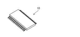
- FIG. 2 is an external perspective view of the light-emitting control device according to the first embodiment of the present disclosure.
- FIG. 3 is a timing chart of the light emission control device in a normal driving state according to the first embodiment of the present disclosure.
- FIG. 4 is an explanatory diagram illustrating an overview of overcurrent protection according to the first embodiment of the present disclosure.
- FIG. 5 is an internal configuration diagram of a light-emitting unit and a lamp number setting circuit according to the first embodiment of the present disclosure.
- FIG. 6 is a diagram showing the relationship between the lamp number control signal and the number of lamps according to the first embodiment of the present disclosure.
- FIG. 7 is a diagram showing the internal configuration of the output voltage monitor circuit and the discharge circuit according to the first embodiment of the present disclosure.
- FIG. 8 is a relationship diagram between the threshold voltage control signal and the monitor voltage according to the first embodiment of the present disclosure.
- FIG. 9 is an explanatory diagram of an overvoltage state according to the first embodiment of the present disclosure.
- FIG. 10 is a diagram showing how the protection threshold voltage changes in response to the threshold voltage control signal according to the first embodiment of the present disclosure.
- FIG. 11 is a timing chart of the light emitting system when the number of lights changes according to the first embodiment of the present disclosure.
- FIG. 12 is a timing chart of the virtual light-emitting system when the number of lights changes according to the reference operation example.
- FIG. 13 is a partial configuration diagram of a light-emitting system according to the second embodiment of the present disclosure.
- FIG. 14 is a relationship diagram of several signals according to the second embodiment of the present disclosure.
- FIG. 15 is an overall configuration diagram of a light-emitting system according to the fourth embodiment of the present disclosure.
- FIG. 16 is a waveform diagram of an enable signal and several voltages according to the fourth embodiment of the present disclosure.
- FIG. 17 is a timing chart of the light emission control device in a stable state according to the fourth embodiment of the present disclosure.
- FIG. 18 is an explanatory diagram of the normal startup control according to the fourth embodiment of the present disclosure.
- FIG. 19 is an explanatory diagram of the slow startup control (SSU control) according to the fourth embodiment of the present disclosure.
- SSU control slow startup control
- FIG. 20 is a timing chart of SSU control according to the first reference operation example.
- FIG. 21 is a timing chart of SSU control according to the first reference operation example.
- FIG. 22 is a diagram for explaining how the on-time of a transistor is controlled to be equal to or longer than the minimum on-time in switching driving.
- FIG. 23 is a diagram for explaining how the on-time of a transistor is controlled to be equal to or longer than the minimum on-time in switching driving.
- FIG. 24 is a timing chart of SSU control according to the second reference operation example.
- FIG. 25 is a timing chart in SSU control according to example EX4_1 belonging to the fourth embodiment of the present disclosure.
- FIG. 26 is an internal circuit diagram of a current adding circuit according to an example EX4_1 belonging to the fourth embodiment of the present disclosure.
- FIG. 27 is a diagram for explaining the operation of the current adding circuit of FIG.
- Ground refers to a reference conductive part having a reference potential of 0V (zero volts), or refers to the potential of 0V itself.
- the reference conductive part may be formed using a conductor such as a metal.
- a potential of 0V is sometimes called ground potential.
- a voltage indicated without a specific reference represents a potential seen from ground.
- Level refers to the level of potential, and for any given signal or voltage, a high level has a higher potential than a low level.
- a switch from a low level to a high level is called an up edge, and a switch from a high level to a low level is called a down edge.
- An up edge may be read as a rising edge.
- a down edge may be read as a falling edge.
- MOSFET field effect transistor
- the on state refers to a state in which the drain and source of the transistor are conductive
- the off state refers to a state in which the drain and source of the transistor are non-conductive (cut-off state).
- MOSFETs are understood to be enhancement-type MOSFETs.
- MOSFET is an abbreviation for "metal-oxide-semiconductor field-effect transistor.”
- the backgate of any MOSFET can be considered to be shorted to the source.
- the on and off states of any transistor may be expressed simply as on and off.
- switching from the off state to the on state will be expressed as turning on, and switching from the on state to the off state will be expressed as turning off.
- the period during which the transistor is in the on state will be referred to as the on period, and the period during which the transistor is in the off state will be referred to as the off period.
- Any switch can be formed using transistors.
- the period during which the signal level is high is called the high level period
- the period during which the signal level is low is called the low level period.
- connections between multiple parts that form a circuit can be understood to refer to electrical connections.
- V1>V2 indicates that voltage V1 is higher than voltage V2
- V1 ⁇ V2 indicates that voltage V1 is lower than voltage V2.
- Fig. 1 shows the overall configuration of a light-emitting system 1 according to the first embodiment of the present disclosure.
- the light-emitting system 1 includes, as main components, a light-emitting control device 10, a light-emitting unit 20, a power conversion circuit 30, an output voltage monitor circuit 40, a resistor 51 and a capacitor 52 for phase compensation, a protection transistor 53, a lamp number setting circuit 60, a discharge circuit 70, an MPU (Micro Processing Unit) 80 which is an example of a processing device, an output capacitor C1, a load switch LDsw, and current detection resistors R1 and R2.
- MPU Micro Processing Unit
- FIG. 2 is an external perspective view of the light emission control device 10.
- the light emission control device 10 is an electronic component that includes a semiconductor chip having a semiconductor integrated circuit formed on a semiconductor substrate, a housing (package) that houses the semiconductor chip, and a plurality of external terminals exposed from the housing to the outside of the light emission control device 10.
- the light emission control device 10 is formed by sealing the semiconductor chip in a housing (package) made of resin. Note that the number of external terminals of the light emission control device 10 and the type of housing of the light emission control device 10 shown in FIG. 2 are merely examples, and can be designed arbitrarily. FIG.
- FIG. 1 shows the power supply terminal IN, enable terminal EN, phase compensation terminal COMP, dimming terminal DIM, gate connection terminal GL, sense terminal CS, ground terminal GND, monitor terminal MN, sense terminals SNSP and SNSN, and drive terminal PDRV, which are included in the plurality of external terminals. Other external terminals are also provided in the light emission control device 10.
- a voltage source VS is connected to the light-emitting system 1.
- the voltage source VS can be considered to be included as a component of the light-emitting system 1.
- the voltage source VS generates and outputs a positive input voltage Vin. Although the input voltage Vin may fluctuate, it is assumed here that the input voltage Vin is a positive DC voltage.
- the input voltage Vin is applied to an input wiring WRin provided outside the light-emitting control device 10.
- the light-emitting unit 20 has a plurality of light-emitting elements 21. Each light-emitting element 21 emits light when supplied with current.
- each light-emitting element 21 is assumed to be a light-emitting diode (LED).
- the light-emitting unit 20 has a high potential end 22 and a low potential end 23, and a series circuit of the plurality of light-emitting elements 21 is connected between the high potential end 22 and the low potential end 23.
- the low potential end 23 is connected to ground.
- the output voltage Vout described below is positive and the load switch LDsw is on, a higher potential is applied to the high potential end 22 than to the low potential end 23.
- Each light-emitting element 21 has a forward direction from the high potential end 22 toward the low potential end 23.
- the power conversion circuit 30 includes a transistor M1, which is an example of a switching element, a coil L1, and a rectifier diode D1, which is an example of a rectifier element.
- the power conversion circuit 30 converts the input voltage Vin to an output voltage Vout (power conversion) through switching drive of the transistor M1.
- the transistor M1 is assumed to be an N-channel MOSFET.
- One end of the coil L1 is connected to the input wiring WRin.
- the other end of the coil L1 is connected to the drain of the transistor M1 and the anode of the rectifier diode D1.
- the gate of the transistor M1 is connected to the gate connection terminal GL.
- the source of the transistor M1 is connected to ground via the current detection resistor R1.
- the source of the transistor M1 is connected to the first end of the current detection resistor R1, and the second end of the current detection resistor R1 is connected to ground.
- the source of the transistor M1 and the first end of the current detection resistor R1 are connected to the sense terminal CS.
- the ground terminal GND is connected to ground.
- the cathode of the rectifier diode D1 is connected to the output terminal OUT.
- the output terminal OUT is connected to ground via the output capacitor C1.
- the voltage applied to the output terminal OUT is the output voltage Vout.
- Output capacitor C1 may be considered to be included as a component of power conversion circuit 30. Note that rectifier diode D1 may be replaced with a synchronous rectifier transistor, and power conversion may be performed to obtain output voltage Vout using a synchronous rectification method.
- the output voltage monitor circuit 40 is connected to the output terminal OUT and generates a monitor voltage Vmn according to the output voltage Vout.
- the monitor voltage Vmn is input to the monitor terminal MN.
- the output voltage monitor circuit 40 generates the monitor voltage Vmn by dividing the output voltage Vout.
- the voltage division ratio for generating the monitor voltage Vmn from the output voltage Vout is variably set according to the threshold voltage control signal Sig2 transmitted from the MPU 80 (details will be described later).
- the first end of the current detection resistor R2 is connected to the output terminal OUT and the sense terminal SNSP. In addition, the first end of the current detection resistor R2 is connected to the emitter of the protection transistor 53.
- the protection transistor 53 is a PNP type bipolar transistor.
- the load switch LDsw is a P-channel type MOSFET.
- the second end of the current detection resistor R2 is connected to the sense terminal SNSN, the base of the protection transistor 53, and the source of the load switch LDsw.
- the gate of the load switch LDsw is connected to the drive terminal PDRV and the collector of the protection transistor 53.
- the drain of the load switch LDsw is connected to the high potential end 22.
- the current flowing through the light-emitting unit 20 is called the drive current and is referred to by the symbol "Idrv".
- the drive current Idrv flowing from the high potential end 22 to the low potential end 23 has positive polarity. "Idrv ⁇ 0" is never true.
- the light-emitting unit 20 emits light with an amount of light that corresponds to the magnitude of the drive current Idrv. Because the drive current Idrv flows through the current detection resistor R2, a voltage drop proportional to the drive current Idrv occurs across the current detection resistor R2.
- the power supply terminal IN is connected to the input wiring WRin. Therefore, an input voltage Vin is applied to the power supply terminal IN.
- a low-level or high-level signal is input to the enable terminal EN from outside the light emission control device 10.
- the phase compensation terminal COMP is connected to one end of a resistor 51, and the other end of the resistor 51 is connected to ground via a capacitor 52.
- the resistor 51 and the capacitor 52 form a phase compensation circuit that compensates for the phase of a comparison voltage Vcmp described below.
- the phase compensation circuit may be built into the light emission control device 10.
- a dimming command signal Sdim is input to the dimming terminal DIM from an external circuit (e.g., MPU 80) of the light emission control device 10.
- the dimming terminal DIM may be composed of two or more external terminals.
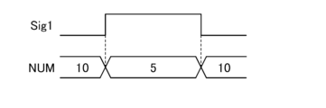
- the lamp number setting circuit 60 variably sets the number of light emitting elements 21 that receive the drive current Idrv and emit light among the light emitting elements 21 provided in the light emitting unit 20 in response to a lamp number control signal Sig1 from the MPU 80.
- the discharge circuit 70 quickly reduces the output voltage Vout by discharging the accumulated charge in the output capacitor C1 at the required timing based on a discharge control signal Sig3 from the MPU 80.
- the lamp number setting circuit 60 and the discharge circuit 70 will be described in detail later.
- the MPU 80 outputs the lamp number control signal Sig1 to the lamp number setting circuit 60, outputs a threshold voltage control signal Sig2 to the output voltage monitor circuit 40, and outputs a discharge control signal Sig3 to the discharge circuit 70.
- the light emission control device 10 includes a current detection circuit 110, a reference voltage generation circuit 120, and a switching control circuit 130.
- the current detection circuit 110 detects the drive current Idrv, and generates and outputs a sense voltage Vsns having a voltage value according to the detection value of the drive current Idrv.
- the reference voltage generation circuit 120 generates and outputs a reference voltage Vref.
- the switching control circuit 130 switches the transistor M1 based on the sense voltage Vsns and the reference voltage Vref. Switching the transistor M1 refers to controlling the transistor M1 to be alternately on and off, and may hereinafter also be referred to simply as switching.
- the output voltage Vout is generated from the input voltage Vin by switching the transistor M1, and the light emission unit 20 emits light when the drive current Idrv based on the output voltage Vout is supplied to the light emission unit 20.
- the internal configuration of the light emission control device 10 will now be described in more detail.
- the enable signal Sen described below has a value of "1" and the load switch LDsw is on.
- the enable signal Sen and the signals Sovp, Suvd, and Socp described below are each binary signals having a value of "0" or "1".
- the current detection circuit 110 has an amplifier 111 and an adder 112.
- the amplifier 111 is connected to the sense terminals SNSP and SNSN, and amplifies and outputs the voltage between the sense terminals SNSP and SNSN.
- the adder 112 adds a predetermined offset voltage Vos to the output voltage of the amplifier 111, and outputs the sum as a sense voltage Vsns. Therefore, the sense voltage Vsns is the sum of the output voltage of the amplifier 111 and the offset voltage Vos.
- the reference voltage generation circuit 120 generates a reference voltage Vref and outputs it to the switching control circuit 130. Immediately after the value of the enable signal Sen switches from “0" to "1", the reference voltage generation circuit 120 can gradually increase the reference voltage Vref from the level of the offset voltage Vos toward a predetermined voltage, but below we consider a state in which the reference voltage Vref is fixed at the predetermined voltage after it has reached that voltage.
- the switching control circuit 130 includes an oscillator 131, an error amplifier 132 (a comparison voltage generating circuit), a slope voltage generating circuit 133, a reset comparator 134, and a drive control circuit 135.
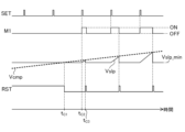
- the oscillator 131 generates and outputs a signal SET having a predetermined frequency fsw.
- the signal SET is a signal that generates a pulse at the frequency fsw (see FIG. 3). That is, a pulse that is at a high level for only a very short time occurs in the signal SET every period of the signal SET.
- the length of one period of the signal SET is the reciprocal of the frequency fsw, and up edges occur in the signal SET at intervals of the reciprocal of the frequency fsw.
- the reciprocal of the frequency fsw is referred to as the switching period or the period of the switching drive.
- the frequency fsw is, for example, within the range of several tens of kHz to several MHz.
- Error amplifier 132 is a current output type transconductance amplifier and has an inverting input terminal, a non-inverting input terminal, and an output terminal.
- a sense voltage Vsns is input to the inverting input terminal of error amplifier 132, and a reference voltage Vref is input to the non-inverting input terminal of error amplifier 132.
- the output terminal of error amplifier 132 is connected to wiring WRcmp.
- the error amplifier 132 generates a voltage corresponding to the difference between the sense voltage Vsns and the reference voltage Vref on the wiring WRcmp by outputting a current signal I132 corresponding to the difference between the sense voltage Vsns and the reference voltage Vref from its output terminal.
- the voltage applied to the wiring WRcmp is called the comparison voltage Vcmp.
- the charge due to the current signal I132 is input/output to/from the wiring WRcmp.
- the error amplifier 132 when the reference voltage Vref is higher than the sense voltage Vsns, the error amplifier 132 outputs a current due to the current signal I132 from the error amplifier 132 to the wiring WRcmp so that the potential of the wiring WRcmp increases, and when the sense voltage Vsns is higher than the reference voltage Vref, the error amplifier 132 draws a current due to the current signal I132 from the wiring WRcmp to the error amplifier 132 so that the potential of the wiring WRcmp decreases. As the absolute value of the difference between the sense voltage Vsns and the reference voltage Vref increases, the magnitude of the current by the current signal I132 also increases.
- the wiring WRcmp is connected to the phase compensation terminal COMP.
- the phase compensation circuit consisting of a resistor 51 and a capacitor 52, receives the input of the current signal I132 and compensates for the phase of the comparison voltage Vcmp.
- the slope voltage generating circuit 133 generates and outputs a slope voltage Vslp having a ramp waveform (see FIG. 3).
- the slope voltage Vslp has information according to the current flowing through the coil L1 (hereinafter referred to as the current information of the coil L1).
- the circuit 133 is connected to the sense terminal CS and the ground terminal GND to receive the voltage across the current detection resistor R1.
- the current flowing through the coil L1 also flows through the current detection resistor R1, so that the voltage across the current detection resistor R1 has the current information of the coil L1.
- the circuit 133 generates a coil information voltage proportional to the voltage across the current detection resistor R1 during the on-period of the transistor M1, and also generates a ramp voltage that gradually increases from 0V during the on-period of the transistor M1.
- the circuit 133 generates a voltage obtained by adding the ramp voltage to the coil information voltage during the on-period of the transistor M1 as the slope voltage Vslp. Therefore, the slope voltage Vslp rises monotonically during the on period of transistor M1.
- the circuit 133 keeps the slope voltage Vslp at or above a predetermined minimum voltage Vslp_min (see FIG. 3).
- the minimum voltage Vslp_min is a positive voltage (e.g., 1.0 V).
- the slope voltage Vslp is fixed at the minimum voltage Vslp_min.
- the comparison voltage Vcmp and the slope voltage Vslp are supplied to the reset comparator 134.
- the reset comparator 134 generates and outputs a signal RST based on the comparison voltage Vcmp and the slope voltage Vslp.
- the inverting input terminal is connected to the wiring WRcmp and receives the comparison voltage Vcmp, and the non-inverting input terminal receives the slope voltage Vslp. Therefore, the reset comparator 134 outputs a low-level signal RST when "Vcmp>Vslp" is true, and outputs a high-level signal RST when "Vcmp ⁇ Vslp" is true.
- the drive control circuit 135 is connected to the gate connection terminal GL. In the normal drive state, the drive control circuit 135 controls the gate potential of the transistor M1 through the gate connection terminal GL based on the signals SET and RST, thereby switching-driving the transistor M1.
- the normal drive state refers to a state in which the enable signal Sen has a value of "1" and no specific abnormality occurs.
- the overvoltage state and the overcurrent state of the light-emitting unit 20 described below belong to the specific abnormalities.
- the drive control circuit 135 In the normal drive state, the drive control circuit 135 repeatedly executes the unit operation of turning on the transistor M1 in response to the rising edge of the signal SET (i.e., switching from the off state to the on state) and then turning off the transistor M1 in response to the rising edge of the signal RST (i.e., switching from the on state to the off state) at a frequency fsw.
- Figure 3 shows the waveforms of several signals in a normal driving state.
- the transistor M1 turns on, and the slope voltage Vslp rises monotonically during the on-period of the transistor M1.
- the reset comparator 134 generates a rising edge in the signal RST.
- the rising edge of the signal RST triggers the transition to the off-period of the transistor M1, and the slope voltage Vslp returns to the minimum voltage Vslp_min, so the high-level period of the signal RST is very short.
- the lower limit of the comparison voltage Vcmp is 0V, but it is maintained at "Vcmp>Vslp_min" during the normal driving state.
- the reference voltage Vref indicates the target value of the drive current Idrv.
- Vref>Vsns causes an increase in the comparison voltage Vcmp, and the increase in the comparison voltage Vcmp increases the on-duty.
- the increase in the on-duty causes an increase in the output voltage Vout, and as a result, the drive current Idrv increases.
- Vref ⁇ Vsns causes a decrease in the comparison voltage Vcmp, and the decrease in the comparison voltage Vcmp decreases the on-duty.
- the decrease in the on-duty causes a decrease in the output voltage Vout, and as a result, the drive current Idrv decreases.
- the switching control circuit 130 controls the value of the drive current Idrv to a current value corresponding to the reference voltage Vref by switching-driving the transistor M1 so as to reduce the difference between the voltages Vref and Vsns (controlling the value of the drive current Idrv to match the above-mentioned target value).
- the on-duty represents the ratio of the on-time of transistor M1 to the sum of the on-time of transistor M1 and the off-time of transistor M1.
- an increase in the on-duty corresponds to an increase in the on-time of transistor M1
- a decrease in the on-duty corresponds to a decrease in the on-time of transistor M1.
- the on-time of transistor M1 refers to the length of the period during which transistor M1 is in the on state in each switching cycle.
- the off-time of transistor M1 refers to the length of the period during which transistor M1 is in the off state in each switching cycle.
- the drive control circuit 135 may set an upper limit on the on-duty and control the on-duty to be below the upper limit.
- the light emission control device 10 is provided with an overvoltage protection circuit 151, a reduced voltage detection circuit 152, a first overcurrent protection circuit 153, and a second overcurrent protection circuit 154.
- the overvoltage protection circuit 151 and the reduced voltage detection circuit 152 are connected to the monitor terminal MN and receive the monitor voltage Vmn.
- the overcurrent protection circuit 153 is connected to the sense terminal CS and the ground terminal GND and receives the voltage across the current detection resistor R1.
- the overcurrent protection circuit 154 receives the sense voltage Vsns.
- the overvoltage protection circuit 151 determines whether the output voltage Vout is in an overvoltage state based on the monitor voltage Vmn, and outputs a signal Sovp indicating the result of the determination.
- the overvoltage state is a state in which the output voltage Vout is equal to or greater than a predetermined protection threshold voltage Vth_ovp.
- the signal Sovp of "1" is an overvoltage protection signal indicating that the output voltage Vout is in an overvoltage state.
- the signal Sovp is input to the drive control circuit 135. During the period in which the signal Sovp has a value of "1", the drive control circuit 135 stops the switching drive of the transistor M1 regardless of the signals SET and RST, and keeps the transistor M1 off.
- the reduced voltage detection circuit 152 determines whether the output voltage Vout is in a reduced voltage state based on the monitor voltage Vmn, and outputs a signal Suvd indicating the determination result.
- the reduced voltage state is a state in which the output voltage Vout is equal to or lower than a predetermined threshold voltage Vth_uvd.
- a signal Suvd of "1” indicates that the output voltage Vout is in a reduced voltage state. "0 ⁇ Vth_uvd ⁇ Vth_ovp" is established.
- a predetermined error signal may be output to an external circuit (not shown) of the light emission control device 10.
- the overcurrent protection circuit 153 detects whether an overcurrent state has occurred in the transistor M1 based on the voltage across the current detection resistor R1. When an overcurrent state in the transistor M1 is detected, the drive control circuit 135 turns off the transistor M1 without waiting for the rising edge of the signal RST.
- the overcurrent protection circuit 154 judges whether the light-emitting unit 20 is in an overcurrent state based on the sense voltage Vsns, and outputs a signal Socp indicating the judgment result.
- a state equivalent to a state in which the high potential end 22 and the low potential end 23 are short-circuited belongs to the overcurrent state of the light-emitting unit 20.
- the circuit 154 sets the value of the signal Socp to "0" as a rule, and sets the value of the signal Socp to "1" when a sense voltage Vsns equal to or greater than a predetermined judgment voltage Vdet_ocp is detected.
- the judgment voltage Vdet_ocp is a judgment voltage for overcurrent.
- the signal Socp of "1" is an overcurrent protection signal indicating that an overcurrent state of the light-emitting unit 20 has been detected.
- a drive current Idrv equal to or greater than a predetermined protection threshold current Ith_ocp is detected (i.e., when it flows through the current detection resistor R2)
- the sense voltage Vsns becomes equal to or greater than the judgment voltage Vdet_ocp. That is, if "Ith_ocp>Idrv", then “Vdet_ocp>Vsns", and if "Ith_ocp ⁇ Idrv", then “Vdet_ocp ⁇ Vsns". Therefore, it can be said that the overcurrent protection circuit 154 detects whether or not a drive current Idrv that is equal to or greater than the protection threshold current Ith_ocp occurs.
- the drive control circuit 135. stops the switching drive of the transistor M1 regardless of the signals SET and RST to keep the transistor M1 off.
- the light emission control device 10 includes a dimming control circuit 155 and a load switch driver 156.
- the dimming control circuit 155 generates and outputs a dimming control signal Scnt based on a dimming command signal Sdim supplied to the dimming terminal DIM.
- the dimming control signal Scnt has a high level or a low level.
- the load switch driver 156 is connected to the drive terminal PDRV, and controls the load switch LDsw to be on or off by controlling the gate potential of the load switch LDsw through the drive terminal PDRV.
- a high level dimming control signal Scnt is a signal that instructs the load switch LDsw to be on
- a low level dimming control signal Scnt is a signal that instructs the load switch LDsw to be off.
- the load switch driver 156 follows the instructions of the dimming control signal Scnt, but the signals Socp and Sovp have priority over the instructions. That is, on condition that the signals Socp and Sovp both have a value of "0", the load switch driver 156 controls the load switch LDsw to be on during the high-level period of the dimming control signal Scnt, and controls the load switch LDsw to be off during the low-level period of the dimming control signal Scnt.
- the driver 156 controls the load switch LDsw to be turned off regardless of the dimming control signal Scnt.
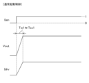
- the driver 156 controls the load switch LDsw to be off regardless of the dimming control signal Scnt. That is, as shown in FIG. 4, when the drive current Idrv equal to or greater than the protection threshold current Ith_ocp is detected in the overcurrent protection circuit 154, the driver 156 controls the load switch LDsw to be off for the hiccup time T HCP regardless of the dimming control signal Scnt.
- the dimming control signal Scnt is fixed to a high level, or the dimming control signal Scnt is alternately switched between a high level and a low level by pulse width modulation.
- the switching drive of the transistor M1 may be performed only during the high level period of the dimming control signal Scnt, and the drive control circuit 135 may fix the transistor M1 to be off during the low level period of the dimming control signal Scnt.
- the dimming control signal Scnt is considered to have a high level.
- a protective transistor 53 is provided to prevent the load switch LDsw from being damaged by this delay. In other words, when the drive current Idrv becomes very large, the protective transistor 53 turns on, immediately turning off the load switch LDsw.
- the light emission control device 10 includes an internal power supply circuit 157 and an enable circuit 158.
- the internal power supply circuit 157 generates one or more internal power supply voltages based on the input voltage Vin.
- Each circuit in the light emission control device 10 is driven based on the input voltage Vin or the internal power supply voltage.
- the enable circuit 158 generates and outputs an enable signal Sen according to the level of the signal supplied to the enable terminal EN. When the enable signal Sen has a value of "0”, each circuit in the light emission control device 10 stops operating, the switching drive of at least the transistor M1 is stopped, and the load switch LDsw is fixed to off. Only when the enable signal Sen has a value of "1", is the switching drive of the transistor M1 permitted and the load switch LDsw controlled to be on.
- FIG. 5 shows the internal configuration of the light-emitting unit 20 and the lamp count setting circuit 60.
- the light-emitting unit 20 includes a series circuit of N light-emitting elements 21.
- N is an integer equal to or greater than 2.
- the variable i described below is an arbitrary integer.
- the light-emitting elements 21 are light-emitting diodes (LEDs), and therefore the light-emitting elements 21 are also referred to as LEDs 21.
- the N LEDs 21 are LEDs 21 [1] to 21 [N]. LEDs 21 [1] to 21 [N] are connected in this order from the high potential end 22 to the low potential end 23. That is, the anode of LED 21 [1] is connected to the high potential end 22.
- the cathode of LED 21 [i] and the anode of LED 21 [i + 1] are connected to node 24 [i].
- the cathode of LED 21 [N] is connected to the low potential end 23.
- the lamp count setting circuit 60 includes transistors 61[1] to 61[N] and a gate driver 62.
- the transistors 61[1] to 61[N] are each an N-channel MOSFET. For each integer i that satisfies "1 ⁇ i ⁇ N”, the transistor 61[i] is connected in parallel to the LED 21[i]. That is, for each integer i that satisfies "1 ⁇ i ⁇ N", the drain of the transistor 61[i] is connected to the anode of the LED 21[i], and the source of the transistor 61[i] is connected to the cathode of the LED 21[i].
- the gate driver 62 is connected to the gates of the transistors 61[1] to 61[N], and controls the gate potential of the transistors 61[1] to 61[N] based on the lamp count control signal Sig1 to individually turn the transistors 61[1] to 61[N] on or off.
- the load switch LDsw Assuming that the load switch LDsw is on and the output voltage Vout is sufficiently high, if the transistor 61[i] is off, the drive current Idrv flows through the LED21[i], causing the LED21[i] to emit light. Even if the load switch LDsw is on and the output voltage Vout is sufficiently high, if the transistor 61[i] is on, the drive current Idrv passes through the transistor 61[i] without flowing through the LED21[i], causing the LED21[i] to not emit light.
- an LED 21 whose corresponding transistor is turned off is referred to as an allowed LED
- an LED 21 whose corresponding transistor is turned on is referred to as a prohibited LED. Therefore, if transistor 61[i] is off, LED 21[i] is an allowed LED, and if transistor 61[i] is on, LED 21[i] is a prohibited LED. Of the allowed and prohibited LEDs, only the allowed LEDs emit light when they receive drive current Idrv. Of LEDs 21[1] to 21[N], the total number of LEDs 21 that are set as allowed LEDs is referred to as the number of lamps and is represented by the symbol "NUM".
- the transistors 61[1] to 61[N] can be individually controlled to be turned on or off, and the lamp count setting circuit 60 can individually set each of the LEDs 21[1] to 21[N] as a light-emitting enabled LED or a light-emitting disabled LED.
- the lamp count control signal Sig1 may be a serial signal or a parallel signal.
- the lamp count control signal Sig1 may be formed from the first to Nth control signals, and the MPU 80 may supply the first to Nth control signals directly to the gates of the transistors 61[1] to 61[N] to individually control the transistors 61[1] to 61[N] to be turned on or off.
- the lamp count setting circuit 60 may employ a method of dividing the LEDs 21[1] to 21[N] into M blocks, and setting the LEDs 21 for each block as light-emitting permitted LEDs or light-emitting prohibited LEDs based on the lamp count control signal Sig1 (hereinafter referred to as the block setting method).
- M represents an integer equal to or greater than 2 and less than N.
- N represents an integer equal to or greater than 2 and less than N.
- LEDs 21[1] to 21[5] are assigned to the first block
- LEDs 21[1] to 21[10] are assigned to the second block.
- the lamp count control signal Sig1, threshold voltage control signal Sig2, and discharge control signal Sig3 output from the MPU 80 are each a binary signal having a high or low signal level.
- the lamp count setting circuit 60 controls transistors 61[1] to 61[10] to be all off, thereby setting all LEDs (LEDs 21[1] to 21[10]) belonging to the first and second blocks as LEDs allowed to emit light, thereby setting the lamp count NUM to 10.
- the lamp count setting circuit 60 controls all transistors 61[1]-61[5] to be off and all transistors 61[6]-61[10] to be on, thereby setting all LEDs belonging to the first block (LED21[1]-21[5]) as LEDs that are allowed to emit light and all LEDs belonging to the second block (LED21[6]-21[10]) as LEDs that are not allowed to emit light, thereby setting the lamp count NUM to 5.
- transistors 61[1]-61[5] may be omitted from the lamp count setting circuit 60 in FIG. 5. In this case, only transistors 61[6]-61[10] are controlled to be on or off according to the lamp count control signal Sig1. Transistors 61[6]-61[10] may be replaced with a single transistor connected in parallel to the series circuit of LEDs 21[6]-21[10], and the lamp count NUM may be switched between 5 and 10 by turning the single transistor on and off.
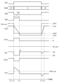
- FIG. 7 shows the internal configuration of the output voltage monitor circuit 40 and the discharge circuit 70.
- the output voltage monitor circuit 40 includes voltage-dividing resistors 41 to 43 and a transistor 44.
- the transistor 44 is an N-channel MOSFET.
- the first end of the voltage-dividing resistor 41 is connected to the output terminal OUT.
- the second end of the voltage-dividing resistor 41 and the first end of the voltage-dividing resistor 42 are commonly connected at a node 45.
- the second end of the voltage-dividing resistor 42, the first end of the voltage-dividing resistor 43, and the drain of the transistor 44 are commonly connected at a node 46.
- the second end of the voltage-dividing resistor 43 and the source of the transistor 44 are connected to ground.
- a threshold voltage control signal Sig2 from the MPU 80 is input to the gate of the transistor 44.
- a divided voltage of the output voltage Vout is generated at the node 45, and the voltage at the node 45 is the monitor voltage Vmn.
- the node 45 is connected to the monitor terminal MN (see FIG. 1).
- the transistor 44 When the threshold voltage control signal Sig2 has a low level, the transistor 44 is off, and when the threshold voltage control signal Sig2 has a high level, the transistor 44 is on.
- R41, R42, and R43 represent the resistance values of the voltage dividing resistors 41, 42, and 43, respectively, and Ron represents the on-resistance value of the transistor 44.
- the on-resistance value Ron is sufficiently smaller than each of the resistance values R41, R42, and R43, and can be considered to be substantially zero. Therefore, if the output voltage Vout is constant as shown in FIG. 8, the monitor voltage Vmn during the period when the transistor 44 is off is higher than the monitor voltage Vmn during the period when the transistor 44 is on.
- the discharge circuit 70 includes a limiting resistor 71 and a transistor 72.
- the transistor 72 is an N-channel MOSFET.
- a first end of the limiting resistor 71 is connected to the output terminal OUT, and a second end of the limiting resistor 72 is connected to the drain of the transistor 72.
- the source of the transistor 72 is connected to ground.
- a discharge control signal Sig3 from the MPU 80 is input to the gate of the transistor 72.
- the transistor 72 When the discharge control signal Sig3 has a low level, the transistor 72 is off, and when the threshold discharge control signal Sig3 has a high level, the transistor 72 is on.
- the transistor 72 When the transistor 72 is on in the state of "Vout>0", a current path that discharges the output capacitor C1 (in other words, a current path that reduces the output voltage Vout, hereinafter referred to as the discharge current path) is formed.
- the high-level discharge control signal Sig3 functions as a signal for forming the discharge current path.
- the accumulated charge of the output capacitor C1 is discharged through the discharge current path.
- the discharge current path is a current path from the output terminal OUT through the limiting resistor 71 and the channel of the transistor 72 to the ground.
- the current flowing through the discharge current path is called the discharge current Idis.
- the discharge current Idis is a current that discharges the output capacitor C1, and the output voltage Vout decreases due to the generation of the discharge current Idis.
- the limiting resistor 71 is provided to limit the magnitude of the discharge current Idis and to adjust the discharge speed. When transistor 72 is off, no discharge current path is formed, and therefore no discharge current Idis is generated.
- a judgment voltage Vdet_ovp is set in advance for the overvoltage protection circuit 151.
- the judgment voltage Vdet_ovp is a voltage for judging whether the output voltage Vout is in an overvoltage state, and has a predetermined fixed voltage value (for example, 1.0 V).
- the circuit 151 detects the magnitude relationship between the output voltage Vout and the protection threshold voltage Vth_ovp by comparing the monitor voltage Vmn with the judgment voltage Vdet_ovp, and generates a signal Sovp based on the comparison result (in other words, based on the detection result of the magnitude relationship).
- the circuit 151 outputs a signal Sovp having a value of "0" when "Vmn ⁇ Vdet_ovp” and outputs a signal Sovp having a value of "1" when "Vmn ⁇ Vdet_ovp".
- hysteresis may be applied when comparing the monitor voltage Vmn and the determination voltage Vdet_ovp.
- the signal Sovp of "1" functions as an overvoltage protection signal indicating that the output voltage Vout is in an overvoltage state, which is a state in which the output voltage Vout is equal to or greater than the protection threshold voltage Vth_ovp.
- the determination voltage Vdet_ovp is fixed, the ratio between the output voltage Vout and the monitor voltage Vmn is variable according to the threshold voltage control signal Sig2. Therefore, as shown in FIG. 10, the protection threshold voltage Vth_ovp changes according to the threshold voltage control signal Sig2.
- the protection threshold voltage Vth_ovp coincides with the first threshold voltage Vth1
- the threshold voltage control signal Sig2 has a low level
- the protection threshold voltage Vth_ovp coincides with the second threshold voltage Vth2.
- the threshold voltage Vth1 is higher than the threshold voltage Vth2.
- the threshold voltages Vth1 and Vth2 are 35 V and 20 V, respectively.
- the threshold voltage control signal Sig2 can be said to be a control signal for variably setting the protection threshold voltage Vth_ovp, or a control signal for switching the protection threshold voltage Vth_ovp between the threshold voltages Vth1 and Vth2.
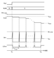
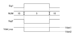
- FIG. 11 shows a timing chart of the light emitting system 1 when the number of lamps NUM changes between 10 and 5.
- the times tA0 to tA1 , tA2 , tA3 , and tA4 occur in this order. Note that from time tA0 to time tA4 and thereafter, the drive current Idrv is maintained below the protection threshold current Ith_ocp, and therefore the signal Socp is "0".
- the lamp number control signal Sig1 is at a low level, so the lamp number NUM is 10 (see also FIG. 6).
- the load switch LDsw is on and the output voltage Vout is stabilized at the appropriate voltage VMM1 .
- the sense voltage Vsns substantially matches the reference voltage Vref, and the value of the drive current Idrv is maintained at the target value IMM according to the reference voltage Vref.
- the MPU 80 switches the lamp number control signal Sig1 from low level to high level at time tA1 .
- the lamp number NUM is changed from 10 to 5 at time tA1 .
- the MPU 80 switches the threshold voltage control signal Sig2 from high level to low level. Therefore, at time tA1 , the threshold voltage control signal Sig2 is switched from high level to low level, and as a result, the protection threshold voltage Vth_ovp drops from threshold voltage Vth1 to threshold voltage Vth2.
- the values of the voltage dividing resistors 41 to 43 are determined so that "Vth1>V MM1 >Vth2" is established.
- the load switch LDsw switches from the on state to the off state, so that the drive current Idrv drops to zero and the switching drive of the transistor M1 is stopped.
- the switching drive of the transistor M1 is stopped, so that the output voltage Vout starts to decrease from time tA1 .
- the decrease in the output voltage Vout is caused by the discharge of the output capacitor C1.
- the path of the discharge current of the output capacitor C1 includes the output voltage monitor circuit 40 (see FIG. 7). However, since the discharge current through the circuit 40 is not large, the slope of the decrease in the output voltage Vout is small only by discharging using the circuit 40.
- the discharge circuit 70 is used to quickly decrease the output voltage Vout. That is, the MPU 80 generates the above-mentioned discharge current Idis by switching the discharge control signal Sig3 from low level to high level at time tA1 (see FIG. 7).
- the discharge control signal Sig3 is set to high level for a predetermined discharge time Tdis, and then the discharge control signal Sig3 is returned to low level. Therefore, in this case, when the discharge time Tdis has elapsed from time tA1 , the discharge control signal Sig3 is returned to the low level. Note that the time when the discharge control signal Sig3 is switched from the low level to the high level may be a very small time after time tA1 .
- the load switch LDsw changes from the off state to the on state, so that the drive current Idrv increases sharply from zero, and the switching drive of the transistor M1 is resumed.
- the time required for the output voltage Vout to decrease from the appropriate voltage VMM1 to the threshold voltage Vth2 can be freely designed by adjusting the value of the limiting resistor 71.
- Fig. 11 it is assumed that the time that is the discharge time Tdis after time tA1 coincides with time tA2 , but the time that is the discharge time Tdis after time tA1 may differ slightly from time tA2 .
- the threshold voltage Vth2 is higher than the appropriate voltage V MM2 .
- the output voltage Vout quickly drops from the threshold voltage Vth2 to the appropriate voltage V MM2 , and is maintained at the appropriate voltage V MM2 until time t A3 .
- the output voltage Vout is maintained at the appropriate voltage VMM2 , and the value of the drive current Idrv is maintained at the target value IMM .
- "Vout ⁇ Vth2" corresponds to "Vmn ⁇ Vdet_ovp.”
- the MPU 80 switches the lamp number control signal Sig1 from high level to low level at time tA3 .
- the lamp number NUM is changed from 5 to 10 at time tA3 .
- the MPU 80 switches the threshold voltage control signal Sig2 from low level to high level.
- the protection threshold voltage Vth_ovp rises from threshold voltage Vth2 to threshold voltage Vth1 at time tA3 .
- the protection threshold voltage Vth_ovp in the overvoltage protection circuit 151 drops from the threshold voltage Vth1 to the threshold voltage Vth2.
- the protection threshold voltage Vth_ovp that is equal to the threshold voltage Vth1 is too large for the second number NUM 2 (here, 5). With a protection threshold voltage Vth_ovp that is too large, it is difficult to achieve proper overvoltage protection. As shown in the operation example of FIG.
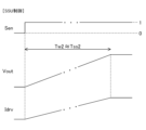
- the virtual light-emitting system is a modification of the light-emitting system 1 in FIG. 1 in which the transistor 44 is fixed to be off and the discharge circuit 70 is deleted (see FIG. 7). Therefore, in the virtual light-emitting system, the ratio between the output voltage Vout and the monitor voltage Vmn is fixed, and the protection threshold voltage Vth_ovp is invariant regardless of the number of lamps NUM. For this reason, in the virtual light-emitting system, it is difficult to provide appropriate overvoltage protection according to the number of lamps NUM.
- the lamp number control signal Sig1 is switched from low level to high level at time t B1 , and the lamp number NUM is changed from 10 to 5.
- the load switch LDsw is turned off and switching drive is stopped for the hiccup time T HCP .
- the output voltage Vout drops slightly below the appropriate voltage V MM1 due to the short-time large drive current Idrv that occurs immediately after time t B1 , but the output voltage Vout hardly changes during the period in which the load switch LDsw is turned off.
- the hiccup operation continues until the output voltage Vout drops to near the appropriate voltage V.
- the hiccup operation here is a repetition of an operation in which the load switch LDsw is turned on and the drive current Idrv reaches the protection threshold current Ith_ocp , and the load switch LDsw is turned off for the hiccup time T and the switching drive is stopped.
- the transition time corresponds to the time difference between times tA1 and tA2 (see FIG. 11).
- the time difference between times tA1 and tA2 can be easily adjusted as desired.
- the transition time can be easily controlled, and the transition from the first light-emitting state to the second light-emitting state can be stably achieved in a short time.
- the protection threshold voltage Vth_ovp is changed by changing the voltage division ratio when generating the monitor voltage Vmn from the output voltage Vout while keeping the determination voltage Vdet_ovp fixed.
- the down edge of the threshold voltage control signal Sig2 functions as a signal for changing the voltage division ratio, and the protection threshold voltage Vth_ovp is lowered from threshold voltage Vth1 to threshold voltage Vth2 by changing the voltage division ratio based on the down edge of the threshold voltage control signal Sig2.
- the high-level and low-level threshold voltage control signals Sig2 can also be said to be signals for setting the protection threshold voltage Vth_ovp to threshold voltages Vth1 and Vth2, respectively.
- the voltage division ratio is fixed regardless of the number of lamps NUM. That is, in the second embodiment, the ratio of the output voltage Vout and the monitor voltage Vmn is fixed regardless of the number of lamps NUM. For this reason, in the MPU 80 according to the second embodiment, it is not necessary to output the threshold voltage control signal Sig2 to the output voltage monitor circuit 40.
- the transistor 44 is deleted from the output voltage monitor circuit 40 in FIG. 7, and Vmn is always "Vout x (R42 + R43) / (R41 + R42 + R43)".
- the voltage division resistors 42 and 43 may be combined into a single resistor.
- a setting terminal OVPSET is added to the light emission control device 10 according to the second embodiment as an external terminal that receives the threshold voltage control signal Sig2'.
- the threshold voltage control signal Sig2' is a binary signal having a high or low signal level.
- the MPU 80 outputs the threshold voltage control signal Sig2' to the light emission control device 10.
- the MPU 80 outputs a high-level threshold voltage control signal Sig2' during a low-level period of the lamp count control signal Sig1, and outputs a low-level threshold voltage control signal Sig2' during a high-level period of the lamp count control signal Sig1.
- the overvoltage protection circuit 151 switches the judgment voltage Vdet_ovp between voltages Vdet1 and Vdet2 based on the threshold voltage control signal Sig2'.
- the voltage Vdet1 has a first predetermined voltage value (e.g., 1.0 V)
- the voltage Vdet2 has a second predetermined voltage value (e.g., 0.7 V) lower than the first predetermined voltage value.
- the overvoltage protection circuit 151 sets the voltage Vdet1 for the judgment voltage Vdet_ovp during a high-level period of the threshold voltage control signal Sig2', and sets the voltage Vdet2 for the judgment voltage Vdet_ovp during a low-level period of the threshold voltage control signal Sig2'.
- the falling edge of the threshold voltage control signal Sig2' functions as a signal for lowering the determination voltage Vdet_ovp (in other words, a signal that instructs the lowering of the determination voltage Vdet_ovp).
- the high-level and low-level threshold voltage control signal Sig2' are signals for setting the protection threshold voltage Vth_ovp to the threshold voltages Vth1 and Vth2, respectively.
- ⁇ Third embodiment>> A third embodiment of the present disclosure will be described.
- a modified technique or applied technique related to the configuration or operation of the above-described light-emitting system 1 will be described.
- the light-emitting system 1 can be used for any purpose.
- the light-emitting system 1 can be mounted on a vehicle such as an automobile, and the light-emitting system 1 can be used for any lighting purpose in the vehicle.
- the number of lamps NUM can be changed when switching between high beam illumination and low beam illumination in the vehicle.
- the light-emitting system 1 can be incorporated into any lighting device installed in the vehicle (e.g., turn lamp, rear lamp, daytime running light), and the light emission pattern of the lighting device can be changed by changing the number of lamps NUM.
- the light-emitting system 1 can be used in a vehicle to form a variable light distribution headlamp (adaptive driving beam).
- the load switch LDsw may be inserted at any position so long as it is a position through which the drive current Idrv flowing through the light-emitting unit 20 passes. That is, in the configuration of FIG. 1, the load switch LDsw is inserted between the second end of the current detection resistor R2 and the high potential end 22, but instead, the load switch LDsw may be inserted between the output terminal OUT and the first end of the current detection resistor R2, or between the low potential end 23 and ground.
- a modified configuration may be adopted in which the low potential end 23 is connected to the input wiring WRin rather than to ground.
- a backflow prevention diode (not shown) may be inserted between the low potential end 23 and the input wiring WRin.
- the low potential end 23 is connected to the anode of the backflow prevention diode, and the cathode of the backflow prevention diode is connected to the input wiring WRin.
- the output voltage Vout is generated by boosting the input voltage Vin, but the output voltage Vout may also be generated by lowering the input voltage Vin.
- a light-emitting control device (10) is configured to generate an output voltage (Vout) from an input voltage (Vin) by switching-driving a switching element (M1), and to supply a drive current (Idrv) based on the output voltage to a light-emitting unit (20) having a series circuit of a plurality of light-emitting elements, thereby causing the light-emitting unit to emit light.
- the light-emitting control device includes a switching control circuit (130) configured to perform the switching drive through state control of the switching element, and an overvoltage protection circuit (Sovp of "1") configured to output an overvoltage protection signal (Sovp of "1") when the output voltage is equal to or higher than a protection threshold voltage (Vth_ovp).
- a switching control circuit 130
- an overvoltage protection circuit Sovp of "1”
- Sovp of "1" configured to output an overvoltage protection signal (Sovp of "1") when the output voltage is equal to or higher than a protection threshold voltage (Vth_ovp).
- a voltage protection circuit in which the switching control circuit stops the switching drive during the output period of the overvoltage protection signal, and when the state of the light-emitting unit is changed from a first state (e.g., a state in which the number of lights NUM is 10) in which the drive current is supplied to a first number of light-emitting elements among the plurality of light-emitting elements to a second state (e.g., a state in which the number of lights NUM is 5) in which the drive current is supplied to a second number of light-emitting elements among the plurality of light-emitting elements that is smaller than the first number, the protection threshold voltage in the overvoltage protection circuit is reduced from a first threshold voltage (Vth1) to a second threshold voltage (Vth2) (first configuration).
- Vth1 first threshold voltage
- Vth2 second threshold voltage
- the appropriate protection threshold voltage differs between the first state and the second state.
- the protection threshold voltage is adjusted according to the number of light-emitting elements to which drive current is supplied among the multiple light-emitting elements connected in series, making it possible to provide appropriate overvoltage protection.
- the light emission control device of the above first configuration may be equipped with a load switch driver (156) configured to control a load switch (LDsw) inserted at a position where the drive current passes based on a dimming control signal (Scnt) to be on, and an overcurrent protection circuit (154) configured to detect whether the drive current is greater than or equal to a protection threshold current (Ith_ocp), and the load switch driver may be configured to control the load switch to be off regardless of the dimming control signal during the output period of the overvoltage protection signal, and when the drive current is detected to be greater than or equal to the protection threshold current, to control the load switch to be off for a predetermined hiccup time (T HCP ) regardless of the dimming control signal (second configuration).
- a load switch driver configured to control a load switch (LDsw) inserted at a position where the drive current passes based on a dimming control signal (Scnt) to be on
- an overcurrent protection circuit configured to detect whether the drive current is greater
- the switching control circuit may be configured (third configuration) to control the value of the drive current to a current value corresponding to the reference voltage by performing the switching drive so as to reduce the difference between a sense voltage (Vsns) corresponding to the drive current and a reference voltage (Vref) during the on period of the load switch.
- Vsns sense voltage
- Vref reference voltage
- the overvoltage protection circuit may detect the magnitude relationship between the output voltage and the protection threshold voltage by comparing a monitor voltage (Vmn) obtained by dividing the output voltage with a judgment voltage (Vdet_ovp), and when the state of the light emission unit is changed from the first state to the second state, the protection threshold voltage may be lowered from the first threshold voltage to the second threshold voltage by changing the voltage division ratio of the output voltage (fourth configuration).
- the overvoltage protection circuit detects the magnitude relationship between the output voltage and the protection threshold voltage by comparing a monitor voltage (Vmn) obtained by dividing the output voltage with a judgment voltage (Vdet_ovp), and the overvoltage protection circuit may be configured (fifth configuration) to lower the protection threshold voltage from the first threshold voltage to the second threshold voltage by lowering the judgment voltage when the state of the light emission unit is changed from the first state to the second state.
- a light-emitting system (1) has a configuration (sixth configuration) including a light-emitting control device (10) according to the second or third configuration, a light-emitting unit (20) that emits light upon receiving the drive current based on the output voltage, an output capacitor (C1) that accumulates a charge equivalent to the output voltage, and a discharge circuit (70) configured to form a current path that discharges the output capacitor when the state of the light-emitting unit changes from the first state to the second state.
- a configuration (sixth configuration) including a light-emitting control device (10) according to the second or third configuration, a light-emitting unit (20) that emits light upon receiving the drive current based on the output voltage, an output capacitor (C1) that accumulates a charge equivalent to the output voltage, and a discharge circuit (70) configured to form a current path that discharges the output capacitor when the state of the light-emitting unit changes from the first state to the second state.
- the overvoltage protection signal is not output, and an output voltage suitable for driving the light-emitting unit in the first state (V MM1 in the example of FIG. 12) is supplied to the light-emitting unit in the second state.
- the output voltage suitable for driving the light-emitting unit in the first state is excessive for the light-emitting unit in the second state.
- a current equivalent to an overcurrent (a driving current equal to or greater than a protection threshold current) repeatedly flows through the light-emitting unit, which may damage the light-emitting unit.
- the protection threshold voltage is lowered from the first voltage to the second threshold voltage (Vth1 to Vth2 in the example of FIG. 11), and the load switch is turned off through the output of the overvoltage protection signal.
- Vth1 to Vth2 in the example of FIG. 11 the protection threshold voltage is lowered from the first voltage to the second threshold voltage (Vth1 to Vth2 in the example of FIG. 11), and the load switch is turned off through the output of the overvoltage protection signal.
- Vth1 to Vth2 in the example of FIG. 11
- the output voltage can be quickly reduced toward a voltage (V MM2 in the example of FIG. 11) suitable for driving the light-emitting unit in the second state by using a discharge circuit.
- the transition time can be easily controlled by adjusting the discharge current, etc., and the first light-emitting state can be stably transitioned to the second light-emitting state in a short time.
- a current equivalent to an overcurrent can be suppressed from flowing to the light-emitting unit during the transition. This leads to improved reliability of the light-emitting unit.
- the light emitting system may further include an output voltage monitor circuit (40) configured to generate a monitor voltage (Vmn) by dividing the output voltage, and the overvoltage protection circuit detects the magnitude relationship between the output voltage and the protection threshold voltage by comparing the monitor voltage with a determination voltage (Vdet_ovp), and when the state of the light emitting unit is changed from the first state to the second state, the output voltage monitor circuit changes the voltage division ratio of the output voltage, thereby lowering the protection threshold voltage from the first threshold voltage to the second threshold voltage (seventh configuration).
- Vmn monitor voltage
- Vdet_ovp determination voltage
- the light-emitting system may further include a lamp number setting circuit (60) configured to variably set the number of light-emitting elements to which the drive current is supplied among the plurality of light-emitting elements, and a processing device (80) configured to switch the state of the light-emitting unit between the first state and the second state by controlling the lamp number setting circuit, and when changing the state of the light-emitting unit from the first state to the second state, the processing device may output a signal for changing the voltage division ratio (e.g., a signal Sig2 with a transition from high level to low level) to the output voltage monitor circuit, thereby lowering the protection threshold voltage from the first threshold voltage to the second threshold voltage, and output a signal for forming the current path (e.g., a high-level signal Sig3) to the discharge circuit (eighth configuration).
- a lamp number setting circuit 60
- a processing device 80
- the processing device may output a signal for changing the voltage division ratio (e.g., a signal Sig2
- the light emitting system may further include an output voltage monitor circuit (40) configured to generate a monitor voltage (Vmn) by dividing the output voltage, and the overvoltage protection circuit detects the magnitude relationship between the output voltage and the protection threshold voltage by comparing the monitor voltage with a judgment voltage (Vdet_ovp), and the overvoltage protection circuit may be configured (ninth configuration) to lower the protection threshold voltage from the first threshold voltage to the second threshold voltage by lowering the judgment voltage when the state of the light emitting unit is changed from the first state to the second state.
- Vmn monitor voltage
- Vdet_ovp a judgment voltage
- the light-emitting system may further include a lamp number setting circuit (60) configured to variably set the number of light-emitting elements to which the drive current is supplied among the plurality of light-emitting elements, and a processing device (80) configured to switch the state of the light-emitting unit between the first state and the second state by controlling the lamp number setting circuit, and the processing device may be configured to output a signal for lowering the determination voltage (e.g., a signal Sig2' with a transition from high level to low level) to the light-emitting control device when changing the state of the light-emitting unit from the first state to the second state, thereby lowering the protection threshold voltage from the first threshold voltage to the second threshold voltage, and output a signal for forming the current path (e.g., a high-level signal Sig3) to the discharge circuit (tenth configuration).
- a lamp number setting circuit 60
- a processing device 80
- the processing device may be configured to output a signal for lowering the determination voltage (e.g
- Fig. 15 shows the overall configuration of a light-emitting system 1A according to the fourth embodiment of the present disclosure.
- the light-emitting system 1A includes, as main components, a light-emitting control device 10A, a light-emitting unit 20, a power conversion circuit 30, an output voltage monitor circuit 40A, a resistor 51 and a capacitor 52 for phase compensation, a protection transistor 53, an output capacitor C1, a load switch LDsw, and current detection resistors R1 and R2.
- the external perspective view of the light emission control device 10A is the same as the external perspective view of the light emission control device 10 shown in FIG. 2.
- the light emission control device 10A is an electronic component that includes a semiconductor chip having a semiconductor integrated circuit formed on a semiconductor substrate, a housing (package) that houses the semiconductor chip, and a plurality of external terminals exposed to the outside of the light emission control device 10A from the housing.
- the light emission control device 10A is formed by sealing the semiconductor chip in a housing (package) made of resin.
- the number of external terminals of the light emission control device 10A and the type of housing of the light emission control device 10A can be designed arbitrarily. FIG.
- the 15 shows the power supply terminal IN, enable terminal EN, phase compensation terminal COMP, dimming terminal DIM, gate connection terminal GL, sense terminal CS, ground terminal GND, monitor terminal MN, sense terminals SNSP and SNSN, and drive terminal PDRV, which are included in the plurality of external terminals.
- Other external terminals are also provided in the light emission control device 10A.
- a voltage source VS is connected to the light-emitting system 1A.
- the voltage source VS can be considered to be included as a component of the light-emitting system 1A.
- the voltage source VS generates and outputs a positive input voltage Vin. Although the input voltage Vin may fluctuate, it is assumed here that the input voltage Vin is a positive DC voltage.
- the input voltage Vin is applied to an input wiring WRin provided outside the light-emitting control device 10A.
- the light-emitting unit 20 has one or more light-emitting elements 21.
- the light-emitting elements 21 emit light when supplied with current.
- the light-emitting unit 20 is assumed to be a series circuit of N light-emitting elements 21, and each light-emitting element 21 is assumed to be a light-emitting diode (LED).
- N represents any integer equal to or greater than 2.
- the light-emitting unit 20 has a high potential end 22 and a low potential end 23, and the series circuit of N light-emitting elements 21 is connected between the high potential end 22 and the low potential end 23.
- the low potential end 23 is connected to ground.
- Each light-emitting element 21 has a forward direction from the high potential end 22 toward the low potential end 23.
- the light-emitting unit 20 includes a first light-emitting diode and a second light-emitting diode as two light-emitting elements 21, the anode of the first light-emitting diode is connected to the high potential end 22, the cathode of the first light-emitting diode and the anode of the second light-emitting diode are connected to each other, and the cathode of the second light-emitting diode is connected to the low potential end 23.
- the power conversion circuit 30 includes a transistor M1, which is an example of a switching element, a coil L1, and a rectifier diode D1, which is an example of a rectifier element.
- the power conversion circuit 30 converts the input voltage Vin to an output voltage Vout (power conversion) through switching drive of the transistor M1.
- the transistor M1 is assumed to be an N-channel MOSFET.
- One end of the coil L1 is connected to the input wiring WRin.
- the other end of the coil L1 is connected to the drain of the transistor M1 and the anode of the rectifier diode D1.
- the gate of the transistor M1 is connected to the gate connection terminal GL.
- the source of the transistor M1 is connected to ground via the current detection resistor R1.
- the source of the transistor M1 is connected to the first end of the current detection resistor R1, and the second end of the current detection resistor R1 is connected to ground.
- the source of the transistor M1 and the first end of the current detection resistor R1 are connected to the sense terminal CS.
- the ground terminal GND is connected to ground.
- the cathode of the rectifier diode D1 is connected to the output terminal OUT.
- the output terminal OUT is connected to ground via the output capacitor C1.
- the voltage applied to the output terminal OUT is the output voltage Vout.
- Output capacitor C1 may be considered to be included as a component of power conversion circuit 30. Note that rectifier diode D1 may be replaced with a synchronous rectifier transistor, and power conversion may be performed to obtain output voltage Vout using a synchronous rectification method.
- the output voltage monitor circuit 40A is connected to the output terminal OUT and generates a monitor voltage Vmn corresponding to the output voltage Vout.
- the monitor voltage Vmn is input to the monitor terminal MN.
- the output voltage monitor circuit 40A includes voltage-dividing resistors 41A and 42A. One end of the voltage-dividing resistor 41A is connected to the output terminal OUT. The other end of the voltage-dividing resistor 41A is connected to ground via the voltage-dividing resistor 42A.
- a monitor voltage Vmn corresponding to a divided voltage of the output voltage Vout is generated at the connection node between the voltage-dividing resistors 41A and 42A.
- the connection node between the voltage-dividing resistors 41A and 42A is connected to the monitor terminal MN, and thus the monitor voltage Vmn is applied to the monitor terminal MN.
- the first end of the current detection resistor R2 is connected to the output terminal OUT and the sense terminal SNSP. In addition, the first end of the current detection resistor R2 is connected to the emitter of the protection transistor 53.
- the protection transistor 53 is a PNP type bipolar transistor.
- the load switch LDsw is a P-channel type MOSFET.
- the second end of the current detection resistor R2 is connected to the sense terminal SNSN, the base of the protection transistor 53, and the source of the load switch LDsw.
- the gate of the load switch LDsw is connected to the drive terminal PDRV and the collector of the protection transistor 53.
- the drain of the load switch LDsw is connected to the high potential end 22.
- the current flowing through the current detection resistor R2 is called the target current and is referred to by the symbol "Itg”.
- the target current Itg flowing from the output terminal OUT to the load switch LDsw has positive polarity. "Itg ⁇ 0" is never true.
- the current flowing through the light-emitting unit 20 is called the drive current and is referred to by the symbol “Idrv”.
- the drive current Idrv flowing from the high potential end 22 to the low potential end 23 has positive polarity. "Idrv ⁇ 0" is never true.
- the light-emitting unit 20 emits light with an amount of light that corresponds to the magnitude of the drive current Idrv.
- the power supply terminal IN is connected to the input wiring WRin. Therefore, an input voltage Vin is applied to the power supply terminal IN.
- a low-level or high-level signal is input to the enable terminal EN from outside the light-emitting control device 10A.
- the phase compensation terminal COMP is connected to one end of a resistor 51, and the other end of the resistor 51 is connected to ground via a capacitor 52.
- the resistor 51 and the capacitor 52 form a phase compensation circuit that compensates for the phase of a comparison voltage Vcmp, which will be described later.
- the phase compensation circuit may be built into the light-emitting control device 10A.
- a dimming command signal Sdim is input to the dimming terminal DIM from an external circuit of the light-emitting control device 10A.
- the dimming terminal DIM may be composed of two or more external terminals.
- the light emission control device 10A includes a current detection circuit 110, a reference voltage generation circuit 120, a switching control circuit 130, and a current addition circuit 140.
- the current detection circuit 110 detects the target current Itg, and generates and outputs a sense voltage Vsns having a voltage value according to the detection value of the target current Itg.
- the reference voltage generation circuit 120 generates and outputs a reference voltage Vref.
- the switching control circuit 130 switches the transistor M1 based on the sense voltage Vsns and the reference voltage Vref.
- the switching drive of the transistor M1 refers to controlling the transistor M1 to be alternately on and off, and may be simply referred to as switching drive below.
- the output voltage Vout is generated from the input voltage Vin by switching the transistor M1, and the light emission unit 20 emits light by supplying a drive current Idrv based on the output voltage Vout to the light emission unit 20.
- the current addition circuit 140 will be described later.
- the internal configuration of the light emission control device 10A will now be described in more detail.
- the enable signal Sen described below has a value of "1" and the load switch LDsw is on.
- the enable signal Sen and the signals Sovp, Suvd, and Socp described below are each binary signals having a value of "0" or "1".
- the current detection circuit 110 has an amplifier 111 and an adder 112.
- the amplifier 111 is connected to the sense terminals SNSP and SNSN, and amplifies and outputs the voltage between the sense terminals SNSP and SNSN.
- the adder 112 adds a predetermined offset voltage Vos to the output voltage of the amplifier 111, and outputs the sum as a sense voltage Vsns. Therefore, the sense voltage Vsns is the sum of the output voltage of the amplifier 111 and the offset voltage Vos.
- the value of the output voltage of the amplifier 111 is expressed as the product of the value of the target current Itg, the value of the current detection resistor R2, and the amplification factor of the amplifier 111, and is positive when "Itg>0".
- the reference voltage generating circuit 120 has an SS circuit 121 and an amplifier 122.
- the SS circuit 121 generates and outputs a voltage Vss.
- the amplifier 122 has a first non-inverting input terminal, a second non-inverting input terminal, an inverting input terminal, and an output terminal.
- the voltage Vss is input to the first non-inverting input terminal of the amplifier 122, and a predetermined voltage Vref0 is input to the second non-inverting input terminal of the amplifier 122.
- the predetermined voltage Vref0 has a fixed voltage value.
- the inverting input terminal and the output terminal of the amplifier 122 are shorted, and the reference voltage Vref is output from the output terminal of the amplifier 122.
- the amplifier 122 is a voltage follower that outputs the lower of the voltage Vss and the predetermined voltage Vref0 as the reference voltage Vref with low impedance.
- Figure 16 shows the relationship between the enable signal Sen, the voltage Vss, and the reference voltage Vref.
- the enable signal Sen has a value of "0”
- the operation of the reference voltage generation circuit 120 is stopped, and the voltages Vss and Vref are 0V.
- the value of the enable signal Sen switches from “0” to "1”.
- the SS circuit 121 sharply increases the voltage Vss from 0V to a predetermined minimum voltage Vss_min, and thereafter monotonically and gradually increases the voltage Vss from the predetermined minimum voltage Vss_min to the predetermined maximum voltage Vss_max.
- the minimum voltage Vss_min is equal to the offset voltage Vos described above.
- “0 ⁇ Vss_min ⁇ Vref0 ⁇ Vss_max” holds.
- the minimum voltage Vss_min is 0.2V
- the specified voltage Vref0 is 2.2V
- the maximum voltage Vss_max is 2.5V.
- the SS circuit 121 can be configured with a DAC (digital-analog converter).
- a circuit (not shown) that supplies a digital signal to the SS circuit 121 as a DAC is provided in the light emission control device 10A so that a voltage Vss having the above-mentioned characteristics can be obtained.
- the switching control circuit 130 includes an oscillator 131, an error amplifier 132 (a comparison voltage generating circuit), a slope voltage generating circuit 133, a reset comparator 134, and a drive control circuit 135.
- the oscillator 131 generates and outputs a signal SET having a predetermined frequency fsw.
- the signal SET is a signal that generates a pulse at the frequency fsw (see FIG. 17). That is, a pulse that is at a high level for only a very short time occurs in the signal SET every period of the signal SET.
- the length of one period of the signal SET is the reciprocal of the frequency fsw, and up edges occur in the signal SET at intervals of the reciprocal of the frequency fsw.
- the reciprocal of the frequency fsw is referred to as the switching period or the period of the switching drive.
- the frequency fsw is, for example, within the range of several tens of kHz to several MHz.
- Error amplifier 132 is a current output type transconductance amplifier and has an inverting input terminal, a non-inverting input terminal, and an output terminal.
- a sense voltage Vsns is input to the inverting input terminal of error amplifier 132, and a reference voltage Vref is input to the non-inverting input terminal of error amplifier 132.
- the output terminal of error amplifier 132 is connected to wiring WRcmp.
- the error amplifier 132 generates a voltage corresponding to the difference between the sense voltage Vsns and the reference voltage Vref on the wiring WRcmp by outputting a current signal I132 corresponding to the difference between the sense voltage Vsns and the reference voltage Vref from its output terminal.
- the voltage applied to the wiring WRcmp is called the comparison voltage Vcmp.
- the charge due to the current signal I132 is input/output to/from the wiring WRcmp.
- the error amplifier 132 when the reference voltage Vref is higher than the sense voltage Vsns, the error amplifier 132 outputs a current due to the current signal I132 from the error amplifier 132 to the wiring WRcmp so that the potential of the wiring WRcmp increases, and when the sense voltage Vsns is higher than the reference voltage Vref, the error amplifier 132 draws a current due to the current signal I132 from the wiring WRcmp to the error amplifier 132 so that the potential of the wiring WRcmp decreases. As the absolute value of the difference between the sense voltage Vsns and the reference voltage Vref increases, the magnitude of the current by the current signal I132 also increases.
- the wiring WRcmp is connected to the phase compensation terminal COMP.
- the phase compensation circuit consisting of a resistor 51 and a capacitor 52, receives the input of the current signal I132 and compensates for the phase of the comparison voltage Vcmp.
- the slope voltage generating circuit 133 generates and outputs a slope voltage Vslp having a ramp waveform (see FIG. 17).
- the slope voltage Vslp has information according to the current flowing through the coil L1 (hereinafter referred to as the current information of the coil L1).
- the circuit 133 is connected to the sense terminal CS and the ground terminal GND to receive the voltage across the current detection resistor R1.
- the current flowing through the coil L1 also flows through the current detection resistor R1, so that the voltage across the current detection resistor R1 has the current information of the coil L1.
- the circuit 133 generates a coil information voltage proportional to the voltage across the current detection resistor R1 during the on-period of the transistor M1, and also generates a ramp voltage that gradually increases from 0V during the on-period of the transistor M1.
- the circuit 133 generates a voltage obtained by adding the ramp voltage to the coil information voltage during the on-period of the transistor M1 as the slope voltage Vslp. Therefore, the slope voltage Vslp rises monotonically during the on period of transistor M1.
- the circuit 133 keeps the slope voltage Vslp at or above a predetermined minimum voltage Vslp_min (see FIG. 17).
- the minimum voltage Vslp_min is a positive voltage (e.g., 1.0 V).
- the slope voltage Vslp is fixed at the minimum voltage Vslp_min.
- the comparison voltage Vcmp and the slope voltage Vslp are supplied to the reset comparator 134.
- the reset comparator 134 generates and outputs a signal RST based on the comparison voltage Vcmp and the slope voltage Vslp.
- the inverting input terminal is connected to the wiring WRcmp and receives the comparison voltage Vcmp, and the non-inverting input terminal receives the slope voltage Vslp. Therefore, the reset comparator 134 outputs a low-level signal RST when "Vcmp>Vslp" is true, and outputs a high-level signal RST when "Vcmp ⁇ Vslp" is true.
- the drive control circuit 135 is connected to the gate connection terminal GL. In the normal drive state, the drive control circuit 135 controls the gate potential of the transistor M1 through the gate connection terminal GL based on the signals SET and RST, thereby switching-driving the transistor M1.
- the normal drive state refers to a state in which the enable signal Sen has a value of "1" and no specific abnormality occurs.
- the overvoltage state and the overcurrent state of the light-emitting unit 20 described below belong to the specific abnormalities.
- the drive control circuit 135 In the normal drive state, the drive control circuit 135 repeatedly executes the unit operation of turning on the transistor M1 in response to the rising edge of the signal SET (i.e., switching from the off state to the on state) and then turning off the transistor M1 in response to the rising edge of the signal RST (i.e., switching from the on state to the off state) at a frequency fsw.
- FIG. 17 shows the waveforms of several signals in a stable state.
- the stable state refers to the normal driving state after time t3.
- the transistor M1 turns on, and the slope voltage Vslp rises monotonically during the on-period of the transistor M1.
- the reset comparator 134 generates an up-edge in the signal RST.
- the up-edge of the signal RST triggers the transition to the off-period of the transistor M1, and the slope voltage Vslp returns to the minimum voltage Vslp_min, so the high-level period of the signal RST is very short.
- the lower limit of the comparison voltage Vcmp is 0V, but it is maintained at "Vcmp>Vslp_min" in the stable state.
- the reference voltage Vref indicates the target value of the target current Itg.
- Vref>Vsns causes an increase in the comparison voltage Vcmp, and the increase in the comparison voltage Vcmp increases the on-duty.
- the increase in the on-duty causes an increase in the output voltage Vout, and as a result, the target current Itg and the drive current Idrv increase.
- Vref ⁇ Vsns causes a decrease in the comparison voltage Vcmp, and the decrease in the comparison voltage Vcmp decreases the on-duty.
- the decrease in the on-duty causes a decrease in the output voltage Vout, and as a result, the target current Itg and the drive current Idrv decrease.
- the switching control circuit 130 controls the value of the target current Itg to a current value corresponding to the reference voltage Vref by switching and driving the transistor M1 so as to reduce the difference between the voltages Vref and Vsns (controlling the value of the target current Itg to match the above-mentioned target value).
- the on-duty represents the ratio of the on-time of transistor M1 to the sum of the on-time of transistor M1 and the off-time of transistor M1.
- an increase in the on-duty corresponds to an increase in the on-time of transistor M1
- a decrease in the on-duty corresponds to a decrease in the on-time of transistor M1.
- the on-time of transistor M1 refers to the length of the period during which transistor M1 is in the on state in each switching cycle.
- the off-time of transistor M1 refers to the length of the period during which transistor M1 is in the off state in each switching cycle.
- the drive control circuit 135 may set an upper limit on the on-duty and control the on-duty to be below the upper limit.
- the current addition circuit 140 is connected to the sense terminal SNSN, and generates the additional current Iadd only under certain conditions.
- the additional current Iadd flows from the sense terminal SNSN to ground. Therefore, when the additional current Iadd is generated, the additional current Iadd flows from the output terminal OUT through the current detection resistor R2, and acts to increase the sense voltage Vsns. The significance of generating the additional current Iadd will be described later.
- the light emission control device 10A is provided with an overvoltage protection circuit 151, a reduced voltage detection circuit 152, a first overcurrent protection circuit 153, and a second overcurrent protection circuit 154.
- the overvoltage protection circuit 151 and the reduced voltage detection circuit 152 are connected to the monitor terminal MN and receive the monitor voltage Vmn.
- the overcurrent protection circuit 153 is connected to the sense terminal CS and the ground terminal GND and receives the voltage across the current detection resistor R1.
- the overcurrent protection circuit 154 receives the sense voltage Vsns.
- the overvoltage protection circuit 151 determines whether the output voltage Vout is in an overvoltage state based on the monitor voltage Vmn, and outputs a signal Sovp indicating the determination result.
- the overvoltage state is a state in which the output voltage Vout is equal to or greater than a predetermined threshold voltage Vth_ovp.
- the circuit 151 generates the signal Sovp based on the result of comparing the output voltage Vout with the threshold voltage Vth_ovp. Specifically, the circuit 151 outputs a signal Sovp having a value of "0" when "Vout ⁇ Vth_ovp", and outputs a signal Sovp having a value of "1" when "Vout ⁇ Vth_ovp".
- hysteresis may be applied when comparing the output voltage Vout with the threshold voltage Vth_ovp.
- a signal Sovp of "1" indicates that the output voltage Vout is in an overvoltage state.
- the signal Sovp is input to the drive control circuit 135. During the period when signal Sovp has a value of "1", drive control circuit 135 stops switching drive of transistor M1 and keeps transistor M1 off, regardless of signals SET and RST.
- the undervoltage detection circuit 152 determines whether the output voltage Vout is in a undervoltage state based on the monitor voltage Vmn, and outputs a signal Suvd indicating the determination result.
- the undervoltage state is a state in which the output voltage Vout is equal to or lower than a predetermined threshold voltage Vth_uvd.
- the circuit 151 generates the signal Suvd based on the result of comparing the output voltage Vout with the threshold voltage Vth_uvd. Specifically, the circuit 151 outputs a signal Suvd having a value of "0" when "Vout>Vth_uvd", and outputs a signal Suvd having a value of "1" when "Vout ⁇ Vth_uvd”.
- hysteresis may be applied when comparing the output voltage Vout with the threshold voltage Vth_uvd.
- a signal Suvd of "1” indicates that the output voltage Vout is in a undervoltage state. "0 ⁇ Vth_uvd ⁇ Vth_ovp" is established.
- a predetermined error signal may be output to an external circuit (not shown) of the light-emitting control device 10A.
- the overcurrent protection circuit 153 detects whether an overcurrent state has occurred in the transistor M1 based on the voltage across the current detection resistor R1. When an overcurrent state in the transistor M1 is detected, the drive control circuit 135 turns off the transistor M1 without waiting for the rising edge of the signal RST.
- the overcurrent protection circuit 154 judges whether the light-emitting unit 20 is in an overcurrent state based on the sense voltage Vsns, and outputs a signal Socp indicating the judgment result.
- a state equivalent to a state in which the high potential end 22 and the low potential end 23 are short-circuited belongs to the overcurrent state of the light-emitting unit 20.
- the circuit 154 sets the value of the signal Socp to "0" as a rule, and sets the value of the signal Socp to "1" when a sense voltage Vsns equal to or greater than a predetermined threshold voltage Vth_ocp is detected.
- the signal Socp of "1" indicates that an overcurrent state of the light-emitting unit 20 has been detected.
- a sense voltage Vsns equal to or greater than the predetermined threshold voltage Vth_ocp is detected
- the value of the signal Socp is maintained at “1” for a certain period of time, and then the value of the signal Socp is returned to "0".
- the signal Socp is input to the drive control circuit 135.
- the drive control circuit 135 stops switching drive of the transistor M1 and keeps the transistor M1 off, regardless of the signals SET and RST.
- the light emission control device 10A includes a dimming control circuit 155 and a load switch driver 156.
- the dimming control circuit 155 generates and outputs a dimming control signal Scnt based on a dimming command signal Sdim supplied to the dimming terminal DIM.
- the dimming control signal Scnt has a high level or a low level.
- the load switch driver 156 is connected to the drive terminal PDRV, and controls the load switch LDsw to be on or off by controlling the gate potential of the load switch LDsw through the drive terminal PDRV.
- a high level dimming control signal Scnt is a signal that instructs the load switch LDsw to be on
- a low level dimming control signal Scnt is a signal that instructs the load switch LDsw to be off.
- the load switch driver 156 follows the instructions of the dimming control signal Scnt, but the signals Socp and Sovp have priority over the instructions. That is, on the condition that the signals Socp and Sovp both have a value of "0", the load switch driver 156 controls the load switch LDsw to be on during the high level period of the dimming control signal Scnt, and controls the load switch LDsw to be off during the low level period of the dimming control signal Scnt.
- the driver 156 controls the load switch LDsw to be off regardless of the dimming control signal Scnt.
- the dimming control signal Scnt is fixed to a high level, or the dimming control signal Scnt is alternately switched between a high level and a low level by pulse width modulation.
- the switching drive of the transistor M1 may be performed only during the high level period of the dimming control signal Scnt, and the drive control circuit 135 may fix the transistor M1 to be off during the low level period of the dimming control signal Scnt. In the following, unless otherwise specified, the dimming control signal Scnt is considered to have a high level.
- the protective transistor 53 is provided to prevent the load switch LDsw from being damaged by this delay. In other words, when the target current Itg becomes very large, the protective transistor 53 turns on, and the load switch LDsw is immediately turned off.
- the light emission control device 10A includes an internal power supply circuit 157 and an enable circuit 158.
- the internal power supply circuit 157 generates one or more internal power supply voltages based on the input voltage Vin.
- Each circuit in the light emission control device 10A is driven based on the input voltage Vin or the internal power supply voltage.
- the enable circuit 158 generates and outputs an enable signal Sen according to the level of the signal supplied to the enable terminal EN. When the enable signal Sen has a value of "0”, each circuit in the light emission control device 10A stops operating, the switching drive of at least the transistor M1 is stopped, and the load switch LDsw is fixed to off. Only when the enable signal Sen has a value of "1", is the switching drive of the transistor M1 permitted and the load switch LDsw controlled to be on.
- normal startup control or slow startup control (hereinafter referred to as SSU control) can be performed.
- SSU control normal startup control or slow startup control
- normal startup control or SSU control is selected and executed according to the input signal level to a setting terminal (not shown).
- the setting terminal is one of the external terminals provided on the light emission control device 10A.
- normal startup control or SSU control is selected and executed based on a signal from an external circuit connected to the light emission control device 10A.
- FIG. 18 shows an overview of normal startup control
- FIG. 19 shows an overview of SSU control
- the output voltage Vout rises from 0V to the stabilized voltage over a relatively short time Tw1 when the value of the enable signal Sen changes from “0” to “1”, and thereafter the output voltage Vout is maintained near the stabilized voltage.
- the output voltage Vout rises from 0V to the stabilized voltage over a relatively long time Tw2 when the value of the enable signal Sen changes from "0" to "1”, and thereafter the output voltage Vout is maintained near the stabilized voltage.
- the drive current Idrv As the output voltage Vout rises, the drive current Idrv also rises.
- the output voltage Vout reaches the stabilized voltage, the light emission brightness of the light emitting unit 20 reaches a target brightness according to the predetermined voltage Vref0.
- the emission luminance of the light-emitting unit 20 may be interpreted as the amount of light emitted by the light-emitting unit 20, and the target luminance may be interpreted as the target amount of light.
- the switching control circuit 130 cooperates with the reference voltage generating circuit 120 to execute normal startup control or SSU control.
- the switching control circuit 130 sets a predetermined time Tss1 for the startup time Tss (see FIG. 16), and at this time, the time Tw1 generally coincides with the predetermined time Tss1 (see FIG. 18).
- the switching control circuit 130 sets a predetermined time Tss2 for the startup time Tss (see FIG. 16), and at this time, the time Tw2 generally coincides with the predetermined time Tss2 (see FIG. 19).
- the predetermined time Tss2 is extremely long compared to the predetermined time Tss1.
- the predetermined time Tss1 is several milliseconds
- the predetermined time Tss2 is several seconds to several tens of seconds.
- the light emission luminance of the light-emitting unit 20 gradually increases from a non-emitting state of the light-emitting unit 20 to the target luminance over a period of several to several tens of seconds, so the process of the light emission luminance of the light-emitting unit 20 gradually increasing can be perceived by the observer. In other words, a visual effect of a gradual increase in the brightness of light emission is obtained.
- the comparison voltage Vcmp is generated so as to reduce the difference between the voltages Vsns and Vref.
- the reference voltage Vref is gradually increased from a predetermined first voltage (Vss_min) toward a predetermined second voltage (Vref0) by the reference voltage generation circuit 120. Therefore, during the execution period of SSU control, the target current Itg gradually increases as the reference voltage Vref increases.
- FIG. 20 and 21 are timing charts of SSU control according to the first reference operation example.
- the value of the signal Sen changes from “0" to “1”
- Times tC1 to tC3 in FIG. 20 are times after time t1 and before time t2, when the comparison voltage Vcmp is near the lower limit of the slope voltage Vslp (i.e., voltage Vslp_min) (times within the dashed circle 610 in FIG. 21).
- the comparison voltage Vcmp reaches the voltage Vslp_min for the first time, and as a result, a down edge occurs in the signal RST, leading to a state in which switching drive can be started.
- an up edge occurs in the signal SET, and the transistor M1 is turned on in response to the up edge of the signal SET.
- the slope voltage Vslp starts to rise above the voltage Vslp_min, and at time t C3 , the state switches from "Vcmp>Vslp" to "Vcmp ⁇ Vslp". Therefore, at time t C3 , an up edge occurs in the signal RST, and as a result, the transistor M1 is turned off.
- the transistor M1 After time tC3 , every time a rising edge occurs in the signal SET, the transistor M1 is turned on, as at time tC2 .
- the comparison voltage Vcmp increases monotonically in conjunction with the increase in the reference voltage Vref (see FIG. 21). Therefore, the on-time of the transistor M1 increases, and as a result, the output voltage Vout increases toward the stabilized voltage and the emission luminance of the light-emitting unit 20 increases toward the target luminance.
- the switching control circuit 130 controls the on-time of the transistor M1 according to the comparison voltage Vcmp, but after turning on the transistor M1, the transistor M1 is kept on for at least the minimum on-time Ton_min regardless of the comparison voltage Vcmp.
- the slope voltage Vslp reaches the comparison voltage Vcmp after the minimum on-time Ton_min or more has elapsed since the transistor M1 is turned on by the rising edge of the signal SET. That is, in the first case, the on-time of the transistor M1 at the time when the slope voltage Vslp reaches the comparison voltage Vcmp is the minimum on-time Ton_min or more.
- the drive control circuit 135 turns off the transistor M1 when the slope voltage Vslp reaches the comparison voltage Vcmp (when it switches from "Vcmp>Vslp" to "Vcmp ⁇ Vslp") as a rule.
- the slope voltage Vslp reaches the comparison voltage Vcmp before the minimum on-time Ton_min has elapsed since the transistor M1 is turned on by the rising edge of the signal SET. That is, in the second case, the on-time of transistor M1 at the time when the slope voltage Vslp reaches the comparison voltage Vcmp is less than the minimum on-time Ton_min. In the second case, the drive control circuit 135 turns off transistor M1 when the on-time of transistor M1 reaches the minimum on-time Ton_min.
- the minimum on-time Ton_min is a predetermined fixed time. In the drive control circuit 135, if an attempt is made to immediately turn off transistor M1 after generating a signal to turn on transistor M1, stable operation of the drive control circuit 135 may not be ensured, and latch-up or the like may occur. By setting a minimum on-time Ton_min, such a situation can be avoided.
- the first reference operation example described above is an operation example assuming that there is no minimum on-time Ton_min.
- the comparison voltage Vcmp reaches the voltage Vslp_min for the first time at time tD1 , and as a result, a down edge occurs in the signal RST, leading to a state in which switching drive can be started.
- an up edge occurs in the signal SET at time tD2 , and the transistor M1 is turned on in response to the up edge of the signal SET.
- the slope voltage Vslp starts to rise from the voltage Vslp_min, and at time tD3 , the state changes from "Vcmp>Vslp" to "Vcmp ⁇ Vslp".
- the time difference between times tD2 and tD3 is shorter than the minimum on-time Ton_min. Therefore, the transistor M1 is maintained on until time tD4 , which is the minimum on-time Ton_min after time tD2 , and the transistor M1 is turned off immediately after time tD4 .
- the minimum on-time Ton_min is excessive for the level of the comparison voltage Vcmp between times tD2 and tD3 .
- the excessive on-time of the transistor M1 generates an excessive target current Itg.
- the excessive target current Itg generates a sense voltage Vsns considerably larger than the reference voltage Vref at that time, and the large sense voltage Vsns significantly reduces the comparison voltage Vcmp.
- the comparison voltage Vcmp starts to decrease immediately after time tD4 , and falls below the voltage Vslp_min at time tD5 .
- the fourth embodiment includes the following examples EX4_1 to EX4_3.
- Example EX4_1 will be described as an example that can suppress the above-mentioned flicker.
- the SSU control according to Example EX4_1 can actually be performed.
- a minimum on-time Ton_min which is a lower limit, is set for the on-time of the transistor M1.
- the operation of the switching control circuit 130 (drive control circuit 135) related to the minimum on-time Ton_min is as described in the second reference operation example (see FIG. 22 and FIG. 23).
- the current adding circuit 140 functions significantly.
- the current adding circuit 140 gradually decreases the additional current Iadd from a predetermined initial current toward 0.
- the initial current has a positive predetermined initial current value I A.
- the current adding circuit 140 performs an additional current generating operation in the SSU control.
- the current adding circuit 140 related to the additional current generating operation generates the additional current Iadd such that the additional current Iadd has the initial current value I A at time t1, and the additional current Iadd gradually and monotonically decreases from the initial current value I A toward zero between times t1 and t2.
- the period from time t1 to time t2 (a period of a predetermined time TSS2 minutes starting from time t1) is the execution period of SSU control.
- Time tJ shown in FIG. 25 is a time after time t1 and before time t2.
- the length of the execution period of the SSU control i.e., time TSS2
- the length between time t1 and time tJ is several hundreds of milliseconds to about 1 second.
- the comparison voltage Vcmp is near the lower limit of the slope voltage Vslp (i.e., voltage Vslp_min), so the light-emission control device 10A performs an operation similar to that of the second reference operation example. That is, between times t1 and tJ , an operation similar to that between times tD1 and tD6 in Fig. 24 is repeatedly performed.
- EX4_1 the current flowing from the output terminal OUT through the current detection resistor R2 between times t1 and tJ flows as an additional current Iadd toward the ground without passing through the light-emitting unit 20 (in other words, it is discarded as a waste current).
- the reference voltage Vref After a while has elapsed since the start of the SSU control, the reference voltage Vref reaches a state where it is sufficiently higher than the voltage Vss_min. In this state, the comparison voltage Vcmp is sufficiently higher than the lower limit of the slope voltage Vslp (i.e., the voltage Vslp_min), and as a result, the on-time of the transistor M1 in each switching period exceeds the minimum on-time Ton_min. Time tJ is the time after this state is reached. Therefore, after time tJ , the switching drive is continued without being stopped due to the comparison voltage Vcmp falling below the lower limit of the slope voltage Vslp, and similarly to the SSU control in the first reference operation example (see FIG. 21), the comparison voltage Vcmp rises monotonically in conjunction with the rise of the reference voltage Vref. For this reason, the on-time of the transistor M1 increases, and as a result, the output voltage Vout rises toward the stabilized voltage.
- the blinking of the light-emitting unit 20 when the light emission luminance is low is suppressed, and flickering of the light-emitting unit 20 when SSU control is being executed is avoided.
- FIG. 26 shows an example of the internal configuration of the current adding circuit 140.
- the current adding circuit 140 includes an operational amplifier 141, a resistor 142, transistors 143 to 147, and a constant current source 148.
- Transistors 143, 146, and 147 are N-channel MOSFETs, and transistors 144 and 145 are P-channel MOSFETs.
- a voltage Va is input to the non-inverting input terminal of the operational amplifier 141.
- the output terminal of the operational amplifier 141 is connected to the gate of the transistor 143.
- the source of the transistor 143 is connected to the inverting input terminal of the operational amplifier 141 and is connected to ground via the resistor 142.
- a positive internal power supply voltage Vreg is applied to each source of transistors 144 and 145.
- the gate and drain of transistor 144 and the gate of transistor 145 are connected to each other.
- Constant current source 148 is connected to the drain of transistor 144 and operates so that a constant current flows between the drain and source of transistor 144.
- the drain of transistor 145, the drain of transistor 143, the drain and gate of transistor 146, and the gate of transistor 147 are connected to each other.
- the sources of transistors 146 and 147 are connected to ground.
- the drain of transistor 147 is connected to the sense terminal SNSN.
- the drain current of transistor 144 generated by the action of constant current source 148 is a constant current Ia.
- a first current mirror circuit is formed by transistors 144 and 145. The first current mirror circuit generates a drain current in transistor 145 that has the same current value as the drain current of transistor 144. Therefore, the drain current of transistor 145 is also equal to the current Ia.
- the drain current of transistor 143 is represented by the symbol "Ib”.
- the drain current of transistor 146 is a current (Ia-Ib) obtained by subtracting the current Ib from the current Ia.
- a second current mirror circuit is formed by transistors 146 and 147. The second current mirror circuit generates a drain current in transistor 147 that has the same current value as the drain current of transistor 146.
- Figure 27 shows the waveforms of voltage Va, current Ib, and added current Iadd.
- the current addition circuit 140 sets voltage Va to 0V at time t1, monotonically and gradually increases voltage Va from 0V to a predetermined voltage Va_max between times t1 and t2, and maintains voltage Va at the predetermined voltage Va_max after time t2.
- Operational amplifier 141 controls the gate potential of transistor 143 so that the voltage across resistor 142 matches voltage Va.
- Example EX4_2 The embodiment EX4_2 of the light-emitting system 1A will be described.
- the current adding circuit 140 monotonically decreases the added current Iadd from time t1 to a specific time, and the added current Iadd becomes zero at the specific time. After the specific time, the added current Iadd is maintained at zero.
- the specific time is time t2.
- the specific time may be a time after time t1 and before time t2 (for example, an intermediate time between times t1 and t2). That is, the added current Iadd may be reduced to zero at the time when "Vss_min ⁇ Vref ⁇ Vref0" is established.
- the specific time may be a time a predetermined time after time t2.
- Example EX4_3 An example EX4_3 of the light emitting system 1A will be described. In the example EX4_3, a modified technique or applied technique related to the configuration or operation of the light emitting system 1A described above will be described.
- the cause of flickering of the light-emitting unit 20 was explained on the assumption that there is a minimum on-time Ton_min. That is, in the second reference operation example, after the start of SU control, when the reference voltage Vref is close to the voltage Vss_min (i.e., the target value of the target current Itg is close to zero), the on-time of the transistor M1 becomes longer than necessary due to the presence of the minimum on-time Ton_min, which causes the light-emitting unit 20 to flicker.
- the minimum on-time Ton_min is determined in the switching control circuit 130 according to each of the above-mentioned embodiments (i.e., the minimum on-time Ton_min does not have to exist). This is because the delay time of the feedback control can be a cause of flickering of the light-emitting unit 20 even if there is no minimum on-time Ton_min.
- the light-emitting system 1A can be used for any purpose.
- the light-emitting system 1A can be mounted on a vehicle such as an automobile, and the light-emitting system 1A can be used for any lighting purpose in the vehicle.
- the load switch LDsw may be inserted at any position so long as it is a position through which the drive current Idrv flowing through the light-emitting unit 20 passes. That is, in the configuration of FIG. 15, the load switch LDsw is inserted between the second end of the current detection resistor R2 and the high potential end 22, but instead, the load switch LDsw may be inserted between the output terminal OUT and the first end of the current detection resistor R2, or between the low potential end 23 and ground.
- a modified configuration may be adopted in which the low potential end 23 is connected to the input wiring WRin rather than to ground.
- a backflow prevention diode (not shown) may be inserted between the low potential end 23 and the input wiring WRin.
- the low potential end 23 is connected to the anode of the backflow prevention diode, and the cathode of the backflow prevention diode is connected to the input wiring WRin.
- the output voltage Vout is generated by boosting the input voltage Vin, but the output voltage Vout may also be generated by lowering the input voltage Vin.
- a light emission control device is a light emission control device (10A) configured to generate an output voltage (Vout) from an input voltage (Vin) by switching-driving a switching element (M1), and to supply a drive current (Idrv) based on the output voltage to a light emission unit (20) to cause the light emission unit to emit light.
- the light emission control device (10A) includes a current detection circuit (110) configured to detect a target current (Itg) including the drive current, a switching control circuit (130) configured to perform the switching drive in response to a detection result of the target current by the current detection circuit, and a current addition circuit (140).
- the switching control circuit executes slow startup control (SSU control) that gradually increases the drive current based on the detection result of the target current
- the current addition circuit is configured to include an additional current (Iadd) in the target current and set the sum of the drive current and the additional current to the target current during the execution period of the slow startup control (eleventh configuration).
- slow startup control provides the visual effect of gradually increasing the brightness of the emitted light.
- the target current is considerably small, so feedback control based on the detection result of the target current may become unstable, and unstable feedback control may cause the light-emitting section to flicker.
- the target current is set to the sum of the drive current and the additional current, including the additional current, during the execution period of the slow startup control.
- feedback control is performed with the additional current added to the target current during the execution period of the slow startup control.
- the feedback control becomes more stable, and flickering of the light-emitting section is also suppressed.
- the current addition circuit may be configured to gradually reduce the additional current as the time elapsed from the start of the slow startup control increases, and to set the drive current to the target current after the slow startup control ends (twelfth configuration).
- the current detection circuit may detect the target current based on the voltage across a current detection resistor (R2) connected in series to the light emission unit, and the current addition circuit may generate the additional current that flows through the current detection resistor from a terminal (OUT) to which the output voltage is applied during the execution period of the slow startup control (thirteenth configuration).
- the light emission control device may further include a reference voltage generation circuit (120) configured to generate a reference voltage (Vref), the current detection circuit generates a sense voltage (Vsns) that rises or falls in response to an increase or decrease in the target current, the reference voltage generation circuit gradually raises the reference voltage from a predetermined first voltage (Vss_min) toward a predetermined second voltage (Vref0) during the execution period of the slow startup control, the switching control circuit performs the switching drive so as to reduce the difference between the sense voltage and the reference voltage, and the target current is gradually increased as the reference voltage rises during the execution period of the slow startup control, thereby gradually increasing the drive current (14th configuration).
- Vref reference voltage generation circuit
- the switching control circuit may have a comparison voltage generating circuit (132) configured to generate a comparison voltage (Vcmp) according to the difference, and control the on-time of the switching element in each cycle of the switching drive according to the comparison voltage, and the switching control circuit may set a lower limit for the on-time of the switching element, and after turning on the switching element, control the on-time of the switching element to be equal to or greater than a predetermined minimum on-time (Ton_min) regardless of the comparison voltage (15th configuration).
- Vcmp comparison voltage
- Ton_min predetermined minimum on-time
- the comparison voltage generating circuit may increase the comparison voltage when the reference voltage is higher than the sense voltage, and decrease the comparison voltage when the sense voltage is higher than the reference voltage, and the switching control circuit may increase the on-time of the switching element in response to an increase in the comparison voltage, and decrease the on-time of the switching element in response to a decrease in the comparison voltage (sixteenth configuration).
- the switching control circuit may be configured to generate a slope voltage (Vslp) whose voltage value gradually increases during the on-period of the switching element in each cycle of the switching drive, and after switching on the switching element, if the on-time of the switching element at the time when the slope voltage reaches the comparison voltage is equal to or greater than the minimum on-time, switch off the switching element at the time when the slope voltage reaches the comparison voltage, and if the on-time of the switching element at the time when the slope voltage reaches the comparison voltage is less than the minimum on-time, switch off the switching element at the time when the on-time of the switching element reaches the minimum on-time (seventh configuration).
- Vslp slope voltage
- the light-emitting system (1) is configured (configuration 18) to include a light-emitting control device (10) according to any of the configurations 11 to 17 above, and a light-emitting unit (20) that emits light upon receiving the drive current based on the output voltage.
- the light-emitting diode (LED) serving as the light-emitting element 21 may be any type of light-emitting diode, and may be an organic LED that realizes organic electroluminescence.
- the light-emitting element 21 may also be one that is not classified as an LED, and may be, for example, a laser diode.
- the channel types of the FETs (field effect transistors) shown in each embodiment are examples.
- the channel type of any FET may be changed between P-channel and N-channel without compromising the above-mentioned spirit.
- any of the transistors described above may be any type of transistor, provided that no disadvantage arises.
- any of the transistors described above as MOSFETs may be replaced with junction FETs, IGBTs (Insulated Gate Bipolar Transistors), or bipolar transistors, provided that no disadvantage arises.
- Any of the transistors has a first electrode, a second electrode, and a control electrode.
- a FET one of the first and second electrodes is the drain, the other is the source, and the control electrode is the gate.
- IGBT In an IGBT, one of the first and second electrodes is the collector, the other is the emitter, and the control electrode is the gate.
- a bipolar transistor that does not belong to the IGBT one of the first and second electrodes is the collector, the other is the emitter, and the control electrode is the base.
Landscapes
- Engineering & Computer Science (AREA)
- Power Engineering (AREA)
- Circuit Arrangement For Electric Light Sources In General (AREA)
Priority Applications (1)
| Application Number | Priority Date | Filing Date | Title |
|---|---|---|---|
| JP2025500673A JPWO2024171593A1 (https=) | 2023-02-15 | 2023-12-13 |
Applications Claiming Priority (4)
| Application Number | Priority Date | Filing Date | Title |
|---|---|---|---|
| JP2023021762 | 2023-02-15 | ||
| JP2023-021762 | 2023-02-15 | ||
| JP2023023054 | 2023-02-17 | ||
| JP2023-023054 | 2023-02-17 |
Publications (1)
| Publication Number | Publication Date |
|---|---|
| WO2024171593A1 true WO2024171593A1 (ja) | 2024-08-22 |
Family
ID=92421187
Family Applications (1)
| Application Number | Title | Priority Date | Filing Date |
|---|---|---|---|
| PCT/JP2023/044593 Ceased WO2024171593A1 (ja) | 2023-02-15 | 2023-12-13 | 発光制御装置及び発光システム |
Country Status (2)
| Country | Link |
|---|---|
| JP (1) | JPWO2024171593A1 (https=) |
| WO (1) | WO2024171593A1 (https=) |
Cited By (1)
| Publication number | Priority date | Publication date | Assignee | Title |
|---|---|---|---|---|
| CN118887924A (zh) * | 2024-09-03 | 2024-11-01 | 深圳市惠程鑫科技有限公司 | 一种led背光源亮度控制系统和方法 |
Citations (2)
| Publication number | Priority date | Publication date | Assignee | Title |
|---|---|---|---|---|
| JP2014216197A (ja) * | 2013-04-25 | 2014-11-17 | パナソニック株式会社 | Led点灯装置および、これを用いた照明器具,照明システム |
| JP2017045653A (ja) * | 2015-08-27 | 2017-03-02 | ミネベア株式会社 | 光源駆動装置 |
-
2023
- 2023-12-13 WO PCT/JP2023/044593 patent/WO2024171593A1/ja not_active Ceased
- 2023-12-13 JP JP2025500673A patent/JPWO2024171593A1/ja active Pending
Patent Citations (2)
| Publication number | Priority date | Publication date | Assignee | Title |
|---|---|---|---|---|
| JP2014216197A (ja) * | 2013-04-25 | 2014-11-17 | パナソニック株式会社 | Led点灯装置および、これを用いた照明器具,照明システム |
| JP2017045653A (ja) * | 2015-08-27 | 2017-03-02 | ミネベア株式会社 | 光源駆動装置 |
Cited By (1)
| Publication number | Priority date | Publication date | Assignee | Title |
|---|---|---|---|---|
| CN118887924A (zh) * | 2024-09-03 | 2024-11-01 | 深圳市惠程鑫科技有限公司 | 一种led背光源亮度控制系统和方法 |
Also Published As
| Publication number | Publication date |
|---|---|
| JPWO2024171593A1 (https=) | 2024-08-22 |
Similar Documents
| Publication | Publication Date | Title |
|---|---|---|
| CN111670609B (zh) | 发光元件驱动控制装置、发光元件驱动电路装置 | |
| US8970136B2 (en) | Semiconductor light source lighting circuit and vehicular lamp | |
| KR101910669B1 (ko) | 발광 소자 구동용 스위칭 전원의 제어 회로 및 그들을 이용한 발광 장치 및 전자 기기 | |
| US8928254B2 (en) | Light emitting diode driver | |
| TWI394485B (zh) | 發光元件驅動電路及其方法 | |
| US7679351B2 (en) | Power supply apparatus | |
| CN100414825C (zh) | 开关式电源电路以及随其配备的电子装置 | |
| US10405386B2 (en) | Light emitting element driving apparatus and driving method thereof | |
| US20120146522A1 (en) | Light emitting diode driver using turn-on voltage of light emitting diode | |
| EP2437134B1 (en) | Low electromagnetic emission driver | |
| US10333024B2 (en) | Ground fault detection for light-emitting element drive device | |
| JP7721560B2 (ja) | 発光素子駆動用半導体集積回路、発光素子駆動装置、発光装置、車両 | |
| CN114325033A (zh) | 电流检测电路 | |
| KR101087749B1 (ko) | 전류 감지기 및 이를 포함하는 발광 다이오드의 구동 장치 | |
| CN111225478B (zh) | 开关组件保护电路 | |
| CN101621876B (zh) | 发光元件驱动电路及其方法 | |
| WO2024171593A1 (ja) | 発光制御装置及び発光システム | |
| JP7411068B2 (ja) | 発光制御装置、発光装置及び車両 | |
| US12557192B2 (en) | Semiconductor device, switching power supply, and lighting device | |
| JP7736488B2 (ja) | 発光素子駆動用半導体集積回路、発光素子駆動装置、発光装置、車両 | |
| JP7797416B2 (ja) | 電源制御装置 | |
| US20250016898A1 (en) | Light-emitting element driving device, light-emitting device, and vehicle | |
| US20250220791A1 (en) | Operating frequency control for light emitting element driving circuit | |
| EP2219422A1 (en) | Discharge lamp lighting circuit having a starter circuit | |
| JP2024154649A (ja) | 発光装置 |
Legal Events
| Date | Code | Title | Description |
|---|---|---|---|
| 121 | Ep: the epo has been informed by wipo that ep was designated in this application |
Ref document number: 23922926 Country of ref document: EP Kind code of ref document: A1 |
|
| WWE | Wipo information: entry into national phase |
Ref document number: 2025500673 Country of ref document: JP |
|
| NENP | Non-entry into the national phase |
Ref country code: DE |
|
| 122 | Ep: pct application non-entry in european phase |
Ref document number: 23922926 Country of ref document: EP Kind code of ref document: A1 |