WO2024162204A1 - 電力変換装置 - Google Patents
電力変換装置 Download PDFInfo
- Publication number
- WO2024162204A1 WO2024162204A1 PCT/JP2024/002385 JP2024002385W WO2024162204A1 WO 2024162204 A1 WO2024162204 A1 WO 2024162204A1 JP 2024002385 W JP2024002385 W JP 2024002385W WO 2024162204 A1 WO2024162204 A1 WO 2024162204A1
- Authority
- WO
- WIPO (PCT)
- Prior art keywords
- control signal
- resonant
- control
- switches
- phase
- Prior art date
- Legal status (The legal status is an assumption and is not a legal conclusion. Google has not performed a legal analysis and makes no representation as to the accuracy of the status listed.)
- Ceased
Links
Images


Classifications
-
- H—ELECTRICITY
- H02—GENERATION; CONVERSION OR DISTRIBUTION OF ELECTRIC POWER
- H02M—APPARATUS FOR CONVERSION BETWEEN AC AND AC, BETWEEN AC AND DC, OR BETWEEN DC AND DC, AND FOR USE WITH MAINS OR SIMILAR POWER SUPPLY SYSTEMS; CONVERSION OF DC OR AC INPUT POWER INTO SURGE OUTPUT POWER; CONTROL OR REGULATION THEREOF
- H02M7/00—Conversion of AC power input into DC power output; Conversion of DC power input into AC power output
- H02M7/42—Conversion of DC power input into AC power output without possibility of reversal
- H02M7/44—Conversion of DC power input into AC power output without possibility of reversal by static converters
- H02M7/48—Conversion of DC power input into AC power output without possibility of reversal by static converters using discharge tubes with control electrode or semiconductor devices with control electrode
-
- Y—GENERAL TAGGING OF NEW TECHNOLOGICAL DEVELOPMENTS; GENERAL TAGGING OF CROSS-SECTIONAL TECHNOLOGIES SPANNING OVER SEVERAL SECTIONS OF THE IPC; TECHNICAL SUBJECTS COVERED BY FORMER USPC CROSS-REFERENCE ART COLLECTIONS [XRACs] AND DIGESTS
- Y02—TECHNOLOGIES OR APPLICATIONS FOR MITIGATION OR ADAPTATION AGAINST CLIMATE CHANGE
- Y02B—CLIMATE CHANGE MITIGATION TECHNOLOGIES RELATED TO BUILDINGS, e.g. HOUSING, HOUSE APPLIANCES OR RELATED END-USER APPLICATIONS
- Y02B70/00—Technologies for an efficient end-user side electric power management and consumption
- Y02B70/10—Technologies improving the efficiency by using switched-mode power supplies [SMPS], i.e. efficient power electronics conversion e.g. power factor correction or reduction of losses in power supplies or efficient standby modes
Definitions
- This disclosure relates to a power conversion device, and more specifically, to a power conversion device capable of converting DC power to AC power.
- Patent document 1 discloses a power conversion device that converts direct current into multi-phase alternating current.
- the power conversion device disclosed in Patent Document 1 includes a main switching means (power conversion circuit), two capacitors, one coil (resonant inductor), multiple auxiliary switch elements, and control means.
- the main switching means is composed of a pair of main switch elements connected in series between both terminals of a DC power source, and a main switching circuit with the interconnection point of the pair of main switch elements as the output point of each phase is provided for each phase of the multi-phase AC.
- the two capacitors divide the voltage of the DC power source.
- One end of the coil is connected to the voltage division point of the two capacitors.
- the multiple auxiliary switch elements connect between the other end of the coil and the output points of each phase.
- control means determines that multiple phase currents flow through the coil, it controls multiple auxiliary switch elements so that the current flowing through at least one phase is smaller than a preset value, and therefore soft switching of the main switch corresponding to the at least one phase is not performed.
- the objective of this disclosure is to provide a power conversion device that can perform soft switching more reliably.
- a power conversion device includes a first DC terminal and a second DC terminal, a power conversion circuit, a plurality of AC terminals, a plurality of switches, a plurality of resonant capacitors, a resonant inductor, a regenerative capacitor, and a control device.
- the power conversion circuit has a plurality of first switching elements and a plurality of second switching elements.
- a plurality of switching circuits in which the plurality of first switching elements and the plurality of second switching elements are connected in series in a one-to-one relationship are connected in parallel to each other.
- the plurality of first switching elements are connected to the first DC terminal, and the plurality of second switching elements are connected to the second DC terminal.
- the plurality of AC terminals correspond one-to-one to the plurality of switching circuits.
- Each of the plurality of AC terminals is connected to a connection point of the first switching element and the second switching element in the corresponding switching circuit.
- the plurality of switches correspond one-to-one to the plurality of switching circuits.
- Each of the plurality of switches has a first end connected to the connection point between the first switching element and the second switching element in the corresponding switching circuit, and a second end commonly connected to a common connection point.
- the resonance capacitors correspond one-to-one to the plurality of switches.
- Each of the plurality of resonance capacitors is connected between the first end and the second DC terminal of the corresponding switch.
- the resonance inductor has a first end and a second end. The first end of the resonance inductor is connected to the common connection point.
- the regeneration capacitor has a third end and a fourth end. The third end of the regeneration capacitor is connected to the first DC terminal or the second DC terminal.
- the control device provides a control signal whose potential changes between a high level and a low level to each of the plurality of first switching elements, the plurality of second switching elements, and the plurality of switches.
- the control device determines that a resonant current flows through each of two or more of the multiple switches simultaneously in the resonant inductor, the control device performs shift control to shift the high-level period of a control signal to at least one of the two or more switches so that the resonant current does not flow through the resonant inductor simultaneously.
- the power conversion device disclosed herein has the advantage of being able to perform soft switching more reliably.
- FIG. 1 is a circuit diagram of a system including a power conversion device according to a first embodiment.
- FIG. 2 is an explanatory diagram of an operation when the control device in the power conversion device performs a basic operation when the load current is greater than 0 and the resonance capacitor is being charged.
- FIG. 3 is another operation explanatory diagram when the control device in the power conversion device performs a basic operation when the load current is greater than 0 and the resonance capacitor is being charged.
- FIG. 4 is a diagram showing a time change in duty and a time change in load current corresponding to voltage commands for each of three phases in an AC load connected to a plurality of AC terminals of the power conversion device according to the above embodiment.
- FIG. 1 is a circuit diagram of a system including a power conversion device according to a first embodiment.
- FIG. 2 is an explanatory diagram of an operation when the control device in the power conversion device performs a basic operation when the load current is greater than 0 and the resonance capacitor is being charged.
- FIG. 3 is another
- FIG. 5 is an explanatory diagram of a first current threshold value and a second current threshold value used by a control device in the power conversion device according to the above embodiment.
- FIG. 6 is an explanatory diagram of an operation when the control device in the power conversion device performs a basic operation when the load current is greater than 0 and the resonant capacitor is discharging.
- FIG. 7 is an explanatory diagram of an operation when the control device in the power conversion device performs a basic operation when the load current is less than 0 and the resonant capacitor is discharging.
- FIG. 8 is an explanatory diagram of an operation when the control device in the power conversion device performs a basic operation when the load current is less than 0 and the resonance capacitor is being charged.
- FIG. 6 is an explanatory diagram of an operation when the control device in the power conversion device performs a basic operation when the load current is greater than 0 and the resonant capacitor is discharging.
- FIG. 7 is an explanatory diagram of an operation when the control device
- FIG. 9 is a timing chart for explaining the operation of the control device in the power conversion device.
- FIG. 10 is a diagram illustrating the operation of a control device in the power conversion device.
- FIG. 11 is a timing chart for explaining the operation of the control device in the power conversion device.
- FIG. 12 is a timing chart for explaining the operation of the control device in the power conversion device according to the second embodiment.
- FIG. 13 is a timing chart for explaining the operation of the control device in the power conversion device.
- FIG. 14 is a timing chart for explaining the operation of the control device in the power conversion device.
- FIG. 15 is a timing chart when the control device executes shift control in the power conversion device according to the third embodiment.
- FIG. 16 is a timing chart of the power conversion device according to the first embodiment when the control device does not execute shift control.
- FIG. 17 is a timing chart when the control device executes shift control in the power conversion device.
- FIG. 18 is a timing chart of the power conversion device according to the first embodiment when the control device does not execute shift control.
- FIG. 19 is a timing chart when the control device executes shift control in the power conversion device according to the fourth embodiment.
- FIG. 20 is a timing chart when the control device executes shift control in the power conversion device according to the fifth embodiment.
- FIG. 21 is a timing chart of the power conversion device according to the first embodiment when the control device does not execute shift control.
- FIG. 22 is a circuit diagram of a system including a power conversion device according to the sixth embodiment.
- FIG. 23 is a circuit diagram of a system including a power conversion device according to the seventh embodiment.
- FIG. 24 is a circuit diagram of a system including a power conversion device according to the eighth embodiment.
- FIG. 25 is a circuit diagram of a system including a power conversion device according to the ninth embodiment.
- FIG. 26 is a circuit diagram of a system including a power conversion device according to the tenth embodiment.
- FIG. 27 is a circuit diagram of a system including a power conversion device according to the eleventh embodiment.
- FIG. 28 is a circuit diagram of a system including a power conversion device according to the twelfth embodiment.
- FIG. 29 is a circuit diagram of a system including a power conversion device according to the thirteenth embodiment.
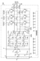
- the power conversion device 100 includes a first DC terminal 31, a second DC terminal 32, and a plurality of (e.g., three) AC terminals 41.
- a DC power source E1 is connected between the first DC terminal 31 and the second DC terminal 32, and an AC load RA1 is connected to the plurality of AC terminals 41.
- the AC load RA1 is, for example, a three-phase motor.
- the power conversion device 100 converts the DC output from the DC power source E1 into AC power and outputs it to the AC load RA1.
- the DC power source E1 includes, for example, a solar cell or a fuel cell.
- the DC power source E1 may include a DC-DC converter.
- the AC power is, for example, three-phase AC power having a U phase, a V phase, and a W phase.
- the power conversion device 100 includes a power conversion circuit 11, a plurality of (e.g., three) switches 8, a plurality of (e.g., three) resonant capacitors 9, a regenerative capacitor 15, a resonant inductor L1, and a control device 50.
- the power conversion device 100 further includes a protection circuit 17 and a capacitor C10.
- Each of the plurality of switches 8 is, for example, a bidirectional switch.
- the power conversion circuit 11 has a plurality of (e.g., three) first switching elements 1 and a plurality of (e.g., three) second switching elements 2.
- a plurality of (e.g., three) switching circuits 10 in which a plurality of first switching elements 1 and a plurality of second switching elements 2 are connected in series in a one-to-one relationship are connected in parallel to each other.
- a plurality of first switching elements 1 are connected to a first DC terminal 31, and a plurality of second switching elements 2 are connected to a second DC terminal 32.
- a plurality of AC terminals 41 correspond one-to-one to the plurality of switching circuits 10.
- Each of the plurality of AC terminals 41 is connected to a connection point 3 of the first switching element 1 and the second switching element 2 in the corresponding switching circuit 10.
- a plurality of switches 8 correspond one-to-one to the plurality of switching circuits 10.
- a first end 81 of each of the plurality of switches 8 is connected to a connection point 3 of the first switching element 1 and the second switching element 2 in the corresponding switching circuit 10.
- a plurality of resonance capacitors 9 correspond one-to-one to the plurality of switches 8.
- Each of the multiple resonant capacitors 9 is connected between the first end 81 of the corresponding switch 8 and the second DC terminal 32.
- the resonant inductor L1 has a first end and a second end, and the first end is connected to the common connection point 25.
- the regenerative capacitor 15 has a third end 153 and a fourth end 154.
- the third end 153 is connected to the second DC terminal 32
- the fourth end 154 is connected to the common connection point 25 via the resonant inductor L1.
- the control device 50 controls the multiple first switching elements 1, the multiple second switching elements 2, and the multiple switches 8.
- the switching circuits 10 corresponding to the U-phase, V-phase, and W-phase of the multiple switching circuits 10 may be referred to as a switching circuit 10U, a switching circuit 10V, and a switching circuit 10W, respectively.
- the first switching element 1 and the second switching element 2 of the switching circuit 10U may be referred to as a first switching element 1U and a second switching element 2U.
- the first switching element 1 and the second switching element 2 of the switching circuit 10V may be referred to as a first switching element 1V and a second switching element 2V.
- the first switching element 1 and the second switching element 2 of the switching circuit 10W may be referred to as a first switching element 1W and a second switching element 2W.
- the connection point 3 between the first switching element 1U and the second switching element 2U may be referred to as the connection point 3U
- the connection point 3 between the first switching element 1V and the second switching element 2V may be referred to as the connection point 3V
- the connection point 3 between the first switching element 1W and the second switching element 2W may be referred to as the connection point 3W.
- the AC terminal 41 connected to the connection point 3U may be referred to as the AC terminal 41U
- the AC terminal 41 connected to the connection point 3V may be referred to as the AC terminal 41V
- the AC terminal 41 connected to the connection point 3W may be referred to as the AC terminal 41W.
- the resonant capacitor 9 connected in parallel to the second switching element 2U may be referred to as the resonant capacitor 9U
- the resonant capacitor 9 connected in parallel to the second switching element 2V may be referred to as the resonant capacitor 9V
- the resonant capacitor 9 connected in parallel to the second switching element 2W may be referred to as the resonant capacitor 9W.
- switch 8U the switch 8 connected to connection point 3U
- switch 8V the switch 8 connected to connection point 3V
- switch 8W the switch 8 connected to connection point 3W
- the high-potential output terminal (positive electrode) of the DC power source E1 is connected to the first DC terminal 31, and the low-potential output terminal (negative electrode) of the DC power source E1 is connected to the second DC terminal 32.
- the U-phase terminal, V-phase terminal, and W-phase terminal of the AC load RA1 are connected to the three AC terminals 41U, 41V, and 41W, respectively.
- each of the multiple (e.g., three) first switching elements 1 and the multiple (e.g., three) second switching elements 2 has a control terminal, a first main terminal, and a second main terminal.
- the control terminals of the multiple first switching elements 1 and the multiple second switching elements 2 are connected to the control device 50.
- the first main terminal of the first switching element 1 is connected to the first DC terminal 31
- the second main terminal of the first switching element 1 is connected to the first main terminal of the second switching element 2
- the second main terminal of the second switching element 2 is connected to the second DC terminal 32.
- the first switching element 1 is a high-side switching element (P-side switching element), and the second switching element 2 is a low-side switching element (N-side switching element).
- Each of the multiple first switching elements 1 and the multiple second switching elements 2 is, for example, an IGBT (Insulated Gate Bipolar Transistor). Therefore, the control terminal, the first main terminal, and the second main terminal of each of the multiple first switching elements 1 and the multiple second switching elements 2 are the gate terminal, the collector terminal, and the emitter terminal, respectively.
- the power conversion circuit 11 further includes a plurality (three) of first diodes 4 connected in anti-parallel to a plurality (three) of first switching elements 1 in a one-to-one relationship, and a plurality (three) of second diodes 5 connected in anti-parallel to a plurality (three) of second switching elements 2 in a one-to-one relationship.
- the anode of the first diode 4 is connected to the second main terminal (emitter terminal) of the first switching element 1 corresponding to the first diode 4
- the cathode of the first diode 4 is connected to the first main terminal (collector terminal) of the first switching element 1 corresponding to the first diode 4.
- the anode of the second diode 5 is connected to the second main terminal (emitter terminal) of the second switching element 2 corresponding to the second diode 5, and the cathode of the second diode 5 is connected to the first main terminal (collector terminal) of the second switching element 2 corresponding to the second diode 5.
- connection point 3U between the first switching element 1U and the second switching element 2U is connected to, for example, the U-phase terminal of the AC load RA1 via the AC terminal 41U.
- connection point 3V between the first switching element 1V and the second switching element 2V is connected to, for example, the V-phase of the AC load RA1 via the AC terminal 41V.
- connection point 3W between the first switching element 1W and the second switching element 2W is connected to, for example, the W-phase of the AC load RA1 via the AC terminal 41W.
- the multiple resonant capacitors 9 correspond one-to-one to the multiple switches 8. Each of the multiple resonant capacitors 9 is connected between a first end of the corresponding switch 8 and the second DC terminal 32.
- the power conversion device 100 has multiple resonant circuits.
- the multiple resonant circuits include a resonant circuit having a resonant capacitor 9U and a resonant inductor L1, a resonant circuit having a resonant capacitor 9V and a resonant inductor L1, and a resonant circuit having a resonant capacitor 9W and a resonant inductor L1.
- the multiple resonant circuits share the resonant inductor L1 in common.
- Each of the multiple switches 8 has, for example, two first IGBTs 6 and second IGBTs 7 connected in inverse parallel.
- the collector terminal of the first IGBT 6 is connected to the emitter terminal of the second IGBT 7, and the emitter terminal of the first IGBT 6 is connected to the collector terminal of the second IGBT 7.
- the emitter terminal of the first IGBT 6 is connected to the connection point 3 of the switching circuit 10 corresponding to the switch 8 having the first IGBT 6.
- the collector terminal of the second IGBT 7 is connected to the connection point 3 of the switching circuit 10 corresponding to the switch 8 having the second IGBT 7.
- the switch 8U is connected to the connection point 3U of the first switching element 1U and the second switching element 2U.
- the switch 8V is connected to the connection point 3V of the first switching element 1V and the second switching element 2V.
- the switch 8W is connected to a connection point 3W between the first switching element 1W and the second switching element 2W.
- the first IGBT 6 and the second IGBT 7 of the switch 8U are referred to as the first IGBT 6U and the second IGBT 7U, respectively
- the first IGBT 6 and the second IGBT 7 of the switch 8V are referred to as the first IGBT 6V and the second IGBT 7V, respectively
- the first IGBT 6 and the second IGBT 7 of the switch 8W are referred to as the first IGBT 6W and the second IGBT 7W, respectively.
- the multiple switches 8 are controlled by the control device 50.
- the first IGBT 6U, the second IGBT 7U, the first IGBT 6V, the second IGBT 7V, the first IGBT 6W, and the second IGBT 7W are controlled by the control device 50.
- the resonant inductor L1 has a first end and a second end. In the resonant inductor L1, the first end of the resonant inductor L1 is connected to the common connection point 25. The second end of the resonant inductor L1 is connected to the fourth end 154 of the regenerative capacitor 15.
- the regenerative capacitor 15 is connected between the second end of the resonant inductor L1 and the second DC terminal 32.
- the regenerative capacitor 15 is, for example, a film capacitor.
- the protection circuit 17 includes a third diode 13 and a fourth diode 14.
- the third diode 13 is connected between the common connection point 25 and the first DC terminal 31.
- the anode of the third diode 13 is connected to the common connection point 25.
- the cathode of the third diode 13 is connected to the first DC terminal 31.
- the fourth diode 14 is connected between the common connection point 25 and the second DC terminal 32.
- the anode of the fourth diode 14 is connected to the second DC terminal 32.
- the cathode of the fourth diode 14 is connected to the common connection point 25. Therefore, the fourth diode 14 is connected in series with the third diode 13.
- Capacitor C10 is connected between the first DC terminal 31 and the second DC terminal 32, and is connected in parallel to the power conversion circuit 11.
- Capacitor C10 is, for example, an electrolytic capacitor.
- the control device 50 controls a plurality of first switching elements 1, a plurality of second switching elements 2, and a plurality of switches 8.
- the execution subject of the control device 50 includes a computer system.
- the computer system has one or more computers.
- the computer system is mainly composed of a processor and a memory as hardware.
- the processor executes a program recorded in the memory of the computer system, thereby realizing the function of the control device 50 as the execution subject in this disclosure.
- the program may be pre-recorded in the memory of the computer system, or may be provided through an electric communication line, or may be recorded and provided on a non-transitory recording medium such as a memory card, an optical disk, or a hard disk drive (magnetic disk) that can be read by the computer system.
- the processor of the computer system is composed of one or more electronic circuits including a semiconductor integrated circuit (IC) or a large-scale integrated circuit (LSI).
- the multiple electronic circuits may be integrated in one chip, or may be distributed across multiple chips.
- the multiple chips may be integrated in one device, or may be distributed across multiple devices.
- the control device 50 outputs control signals SU1, SV1, SW1 that control the on/off of each of the multiple first switching elements 1U, 1V, 1W.
- Each of the control signals SU1, SV1, SW1 is, for example, a PWM (Pulse Width Modulation) signal whose potential level changes between a first potential level (hereinafter also referred to as a low level) and a second potential level (hereinafter also referred to as a high level) that is higher than the first potential level.
- the first switching elements 1U, 1V, 1W are in an on state when the control signals SU1, SV1, SW1 are at a high level, and in an off state when the control signals SU1, SV1, SW1 are at a low level.
- the control device 50 also outputs control signals SU2, SV2, SW2 that control the on/off of each of the multiple second switching elements 2U, 2V, 2W.
- Each of the control signals SU2, SV2, and SW2 is, for example, a PWM signal whose potential level changes between a first potential level (hereinafter also referred to as a low level) and a second potential level (hereinafter also referred to as a high level) that is higher than the first potential level.
- the second switching elements 2U, 2V, and 2W are turned on when the control signals SU2, SV2, and SW2 are at a high level, and turned off when they are at a low level.
- the control device 50 uses a sawtooth carrier signal (see FIG. 2) to generate control signals SU1, SV1, SW1 corresponding to each of the first switching elements 1U, 1V, 1W, and control signals SU2, SV2, SW2 corresponding to each of the second switching elements 2U, 2V, 2W. More specifically, the control device 50 generates control signals SU1, SU2 to be provided to the first switching element 1U and the second switching element 2U, respectively, based on at least the carrier signal and a voltage command for the U phase. The control device 50 also generates control signals SV1, SV2 to be provided to the first switching element 1V and the second switching element 2V, respectively, based on at least the carrier signal and a voltage command for the V phase.
- a sawtooth carrier signal see FIG. 2
- the control device 50 also generates control signals SW1, SW2 to be provided to the first switching element 1W and the second switching element 2W, respectively, based on at least the carrier signal and a voltage command for the W phase.
- the U-phase voltage command, V-phase voltage command, and W-phase voltage command are, for example, sinusoidal signals with phases differing from each other by 120°, and the amplitude (voltage command value) of each changes over time.
- the waveform of the carrier signal is not limited to a sawtooth waveform, and may be, for example, a triangular wave or a sawtooth wave obtained by inverting the sawtooth wave in FIG. 2.
- the length of one cycle of the U-phase voltage command, V-phase voltage command, and W-phase voltage command is the same.
- the length of one cycle of the U-phase voltage command, V-phase voltage command, and W-phase voltage command is longer than the length of one cycle of the carrier signal.
- the duty of the control signal SU1 is shown as the U-phase duty.
- the control device 50 compares the U-phase voltage command with the carrier signal to generate the control signal SU1 to be provided to the first switching element 1U.
- the control device 50 also inverts the control signal SU1 to be provided to the first switching element 1U to generate the control signal SU2 to be provided to the second switching element 2U.
- the control device 50 also sets a dead time period Td (see FIG. 2) between the high-level period of the control signal SU1 and the high-level period of the control signal SU2 so that the on periods of the first switching element 1U and the second switching element 2U do not overlap.
- the duty of the control signal SV1 is shown as the V-phase duty.
- the control device 50 compares the V-phase voltage command with the carrier signal to generate the control signal SV1 to be provided to the first switching element 1V.
- the control device 50 also inverts the control signal SV1 to be provided to the first switching element 1V to generate the control signal SV2 to be provided to the second switching element 2V.
- the control device 50 also sets a dead time period Td (see FIG. 2) between the high-level period of the control signal SV1 and the high-level period of the control signal SV2 so that the on periods of the first switching element 1V and the second switching element 2V do not overlap.
- the duty of the control signal SW1 is shown as the W phase duty.
- the control device 50 compares the voltage command of the W phase with the carrier signal to generate the control signal SW1 to be provided to the first switching element 1W.
- the control device 50 also inverts the control signal SW1 to be provided to the first switching element 1W to generate the control signal SW2 to be provided to the second switching element 2W.
- the control device 50 also sets a dead time period Td (see FIG. 3) between the high level period of the control signal SW1 and the high level period of the control signal SW2 so that the on periods of the first switching element 1W and the second switching element 2W do not overlap.
- the U-phase voltage command, V-phase voltage command, and W-phase voltage command are, for example, sinusoidal signals whose phases differ by 120°, and whose amplitudes change over time. Therefore, the duty of the control signal SU1 (U-phase duty), the duty of the control signal SV1 (V-phase duty), and the duty of the control signal SW1 (W-phase duty) change into sinusoidal waves whose phases differ by 120°, for example, as shown in FIG. 4. Similarly, the duty of the control signal SU2, the duty of the control signal SV2, and the duty of the control signal SW2 change into sinusoidal waves whose phases differ by 120°.
- the control device 50 generates the control signals SU1, SU2, SV1, SV2, SW1, and SW2 based on the carrier signal, the voltage commands, and information about the state of the AC load RA1.
- the information about the state of the AC load RA1 includes, for example, detection values from a plurality of current sensors that detect output currents (hereinafter also referred to as load currents) iU, iV, and iW that flow through the U-phase, V-phase, and W-phase of the AC load RA1, respectively.
- the multiple switches 8, the resonant inductor L1, the multiple resonant capacitors 9, and the regenerative capacitor 15 are provided to perform zero-voltage soft switching of the multiple first switching elements 1 and the multiple second switching elements 2.
- control device 50 controls a plurality of switches 8 in addition to a plurality of first switching elements 1 and second switching elements 2 of the power conversion circuit 11.
- the control device 50 generates control signals SU6, SU7, SV6, SV7, SW6, SW7 that control the on/off of the first IGBT6U, the second IGBT7U, the first IGBT6V, the second IGBT7V, the first IGBT6W, and the second IGBT7W, and outputs them to the gate terminals of the first IGBT6U, the second IGBT7U, the first IGBT6V, the second IGBT7V, the first IGBT6W, and the second IGBT7W.
- the switch 8U can pass a charging current that flows through the path of the regenerative capacitor 15 - resonant inductor L1 - switch 8U - resonant capacitor 9U.
- the charging current is a current that charges the resonant capacitor 9U.
- the switch 8U can pass a discharging current that flows through the path of the resonant capacitor 9U - switch 8U - resonant inductor L1 - regenerative capacitor 15.
- the discharging current is a current that discharges the charge in the resonant capacitor 9U.
- the switch 8V can pass a charging current that flows through the path of the regenerative capacitor 15 - resonant inductor L1 - switch 8V - resonant capacitor 9V.
- the charging current is a current that charges the resonant capacitor 9V.
- the switch 8V can pass a discharging current that flows through the path of the resonant capacitor 9V - switch 8V - resonant inductor L1 - regenerative capacitor 15.
- the discharging current is a current that discharges the charge of the resonant capacitor 9V.
- the switch 8W can pass a charging current that flows through the path of the regenerative capacitor 15 - resonant inductor L1 - switch 8W - resonant capacitor 9W.
- the charging current is a current that charges the resonant capacitor 9W.
- the switch 8W can pass a discharging current that flows through the path of the resonant capacitor 9W - switch 8W - resonant inductor L1 - regenerative capacitor 15.
- the discharging current is a current that discharges the charge of the resonant capacitor 9W.
- the polarity of the current iL1 flowing through the resonant inductor L1 is defined as positive when it flows in the direction of the arrow in Fig. 1, and the polarity of the current flowing in the opposite direction to the direction of the arrow in Fig. 1 is defined as negative.
- the polarity of the load currents iU, iV, and iW flowing through the U-phase, V-phase, and W-phase of the AC load RA1 is defined as positive when it flows in the direction of the arrow in Fig.
- the first IGBT 6U of the switch 8U may change from an ON state in which the current iL1 flows through the resonant inductor L1 with positive polarity to an OFF state.
- the current iL1 flowing through the resonant inductor L1 is regenerated to the power conversion circuit 11 via the third diode 13 until the energy of the resonant inductor L1 is consumed and the current iL1 becomes zero.
- the second IGBT 7U of the switch 8U may change from an ON state in which the current iL1 flows through the resonant inductor L1 with negative polarity to an OFF state.
- the current iL1 flowing through the resonant inductor L1 flows through the path of the fourth diode 14-resonant inductor L1-regenerative capacitor 15 until the energy of the resonant inductor L1 is consumed and the current iL1 becomes zero.
- the first IGBT 6V of the switch 8V may change from an ON state in which the current iL1 flows through the resonant inductor L1 with positive polarity to an OFF state in which the first IGBT 6V of the switch 8V.
- the current iL1 flowing through the resonant inductor L1 is regenerated to the power conversion circuit 11 via the third diode 13 until the energy of the resonant inductor L1 is consumed and the current iL1 becomes zero.
- the second IGBT 7V of the switch 8V may change from an ON state in which the current iL1 flows through the resonant inductor L1 with negative polarity to an OFF state in which the second IGBT 7V of the switch 8V.
- the current iL1 flowing through the resonant inductor L1 may flow through the path of the fourth diode 14-resonant inductor L1-regenerative capacitor 15 until the energy of the resonant inductor L1 is consumed and the current iL1 becomes zero.
- the first IGBT 6W of the switch 8W may be turned off from a state in which the first IGBT 6W of the switch 8W is on and the current iL1 flows through the resonant inductor L1 with positive polarity.
- the current iL1 flowing through the resonant inductor L1 is regenerated to the power conversion circuit 11 via the third diode 13 until the energy of the resonant inductor L1 is consumed and the current iL1 becomes zero.
- the second IGBT 7W of the switch 8W may be turned off from a state in which the second IGBT 7W of the switch 8W is on and the current iL1 flows through the resonant inductor L1 with negative polarity.
- the current iL1 flowing through the resonant inductor L1 flows through the path of the fourth diode 14 - resonant inductor L1 - regenerative capacitor 15 until the energy of the resonant inductor L1 is consumed and the current iL1 becomes zero.
- the control device 50 sets a dead time period Td between the high level period of the control signals SU1, SV1, SW1 to the first switching elements 1U, 1V, 1W and the high level period of the control signals SU2, SV2, SW2 to the second switching elements 2U, 2V, 2W for each of the multiple switching circuits 10.
- the basic operation is an operation when no resonant current flows through two or more of the multiple switches 8 simultaneously in the resonant inductor L1. After explaining the basic operation, we will explain the operation when the control device 50 determines that a resonant current flows through two or more of the multiple switches 8 simultaneously.
- the basic operation of the control device 50 differs depending on the polarity (positive/negative) of the load current flowing through the AC terminal 41 connected to the target switching element and the operation (charging operation/discharging operation) of the resonant capacitor 9 connected in series or parallel to the target switching element.
- the load current has positive polarity when it flows from the AC terminal 41 to the AC load RA1, and has negative polarity when it flows from the AC load RA1 to the AC terminal 41.
- the resonant capacitor 9 is charging, the voltage across the resonant capacitor 9 increases.
- the resonant capacitor 9 is discharging, the voltage across the resonant capacitor 9 decreases.
- the voltage across each of the multiple second switching elements 2 is the same as the voltage across the resonant capacitor 9 connected in parallel to the second switching element 2.
- the control device 50 turns on the first IGBT 6 corresponding to the target first switching element 1.
- the control device 50 causes the resonant inductor L1 and the resonant capacitor 9 connected to the target first switching element 1 to resonate, charging the resonant capacitor 9 from the regenerative capacitor 15, and setting the voltage across the target first switching element 1 to zero.
- the power conversion device 100 can realize zero-voltage soft switching of the target first switching element 1.
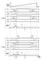
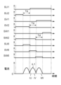
- FIG. 2 illustrates the control signals SU1 and SU2 given from the control device 50 to the first switching element 1U and the second switching element 2U of the switching circuit 10U when the target first switching element is the first switching element 1U of the switching circuit 10U.
- FIG. 2 illustrates the control signal SU6 given from the control device 50 to the first IGBT 6U of the switch 8U, the load current iU flowing in the U-phase of the AC load RA1, the current iL1 flowing in the resonant inductor L1, the voltage V1u across the first switching element 1U, and the voltage V2u across the second switching element 2U.
- FIG. 1 illustrates the control signals SU1 and SU2 given from the control device 50 to the first switching element 1U and the second switching element 2U of the switching circuit 10U when the target first switching element is the first switching element 1U of the switching circuit 10U.
- FIG. 2 illustrates the control signal SU6 given from the control device 50 to the first IGBT 6U of the switch 8U,
- FIG. 2 illustrates the control signals SV1 and SV2 given from the control device 50 to the first switching element 1V and the second switching element 2V of the switching circuit 10V when the target first switching element is the first switching element 1V of the switching circuit 10V.
- FIG. 2 also illustrates the control signal SV6 provided from the control device 50 to the first IGBT 6V of the switch 8V, the load current iV flowing through the V phase of the AC load RA1, the current iL1 flowing through the resonant inductor L1, the voltage V1v across the first switching element 1V, and the voltage V2v across the second switching element 2V.
- FIG. 2 also shows the dead time period Td set in the control device 50 to prevent the first switching element 1 and the second switching element 2, which are in phase, from being turned on at the same time.
- FIG. 2 also shows the additional time Tau set in the control device 50 for the control signal SU6 of the first IGBT 6U of the switch 8U, and the additional time Tav set in the control device 50 for the control signal SV6 of the first IGBT 6V of the switch 8V.
- the additional time Tau and the additional time Tav will be described later.
- FIG. 3 illustrates control signals SW1 and SW2 provided from the control device 50 to the first switching element 1W and the second switching element 2W of the switching circuit 10W, respectively, when the target first switching element is the first switching element 1W of the switching circuit 10W.
- FIG. 3 also illustrates the control signal SW6 provided from the control device 50 to the first IGBT 6W of the switch 8W, and the load current iW flowing through the W phase of the AC load RA1.
- FIG. 3 also illustrates the current iL1 flowing through the resonant inductor L1.
- FIG. 3 also illustrates the voltage V1w across the first switching element 1W and the voltage V2w across the second switching element 2W.
- the voltage value of the DC power source E1 is illustrated as Vd.
- FIG. 3 also illustrates the dead time period Td that is set in the control device 50 to prevent the first switching element 1W and the second switching element 2W from being turned on at the same time.
- FIG. 3 also illustrates the additional time Taw that is set in the control device 50 for the control signal SW6 of the first IGBT 6W of the switch 8W. The additional time Taw will be described later.
- the above-mentioned additional time Tau is a time set to advance the start time t1 of the high level period of the control signal SU6 to be earlier than the start time t2 of the dead time period Td, so that the high level period of the control signal SU6 is longer than the dead time period Td, as shown in FIG. 2.
- the length of the additional time Tau is set based on the value of the load current iU. In order to start LC resonance from the start time t2 of the dead time period Td, it is desirable that the value of the current iL1 matches the value of the load current iU at the start time t2 of the dead time period Td.
- the end time of the high level period of the control signal SU6 may be the same as or later than the end time t3 of the dead time period Td.
- FIG. 2 shows an example in which the end time of the high level period of the control signal SU6 is set to be the same as the end time t3 of the dead time period Td.
- the control device 50 sets the high-level period of the control signal SU6 to Tau+Td.
- the voltage V2u across the second switching element 2U becomes Vd at the end time t3 of the dead-time period Td
- the voltage V1u across the first switching element 1U becomes zero at the end time t3 of the dead-time period Td.
- the current iL1 flowing through the resonance inductor L1 starts to flow at the start time t1 of the high-level period of the control signal SU6, and becomes zero at the time t4 when the additional time Tau has elapsed from the end time t3 of the dead-time period Td.
- the current iL1 since iL1 ⁇ iU is satisfied from the start time t2 of the dead-time period Td, the current iL1 in the shaded area of the current waveform in the fifth row from the top in FIG. 2 flows into the resonance capacitor 9U, and LC resonance occurs. After the end time t3 of the dead time period Td, the current iL1 is regenerated in the power conversion circuit 11 via the third diode 13 that is directly connected to the resonant inductor L1.
- the resonance half period in the case of basic operation is half the resonance period, which is the reciprocal of the resonance frequency of the resonance circuit including the resonance inductor L1 and one resonance capacitor 9. Therefore, when the inductance of the resonance inductor L1 is L and the capacitance of the resonance capacitor 9 is C, the resonance half period is ⁇ (L ⁇ C) 1/2 .
- the resonance half period in the basic operation is set to be the same as the length of the dead time period Td, for example.
- the above-mentioned additional time Tav is a time set to advance the start time t5 of the high level period of the control signal SV6 to be earlier than the start time t6 of the dead time period Td, so that the high level period of the control signal SV6 is longer than the dead time period Td, as shown in FIG. 2.
- the length of the additional time Tav is set based on the value of the load current iV. In order to start LC resonance from the start time t6 of the dead time period Td, it is desirable that the value of the current iL1 matches the value of the load current iV at the start time t6 of the dead time period Td.
- the end time of the high level period of the control signal SV6 may be the same as the end time t7 of the dead time period Td or later.
- FIG. 2 shows an example in which the end time of the high level period of the control signal SV6 is set to be the same as the end time t7 of the dead time period Td.
- the control device 50 sets the high-level period of the control signal SV6 to Tav+Td.
- the voltage V1V across the first switching element 1V becomes zero at the end point t7 of the dead-time period Td.
- the current iL1 flowing through the resonant inductor L1 starts to flow at the start point t5 of the high-level period of the control signal SV6, and becomes zero at the time point t8 when the additional time Tav has elapsed from the end point t7 of the dead-time period Td.
- the current iL1 since iL1 ⁇ iV from the start point t6 of the dead-time period Td, the current iL1 in the shaded area of the current waveform in the 10th row from the top in FIG. 2 flows into the resonant capacitor 9V, and LC resonance occurs.
- the current iL1 is regenerated to the power conversion circuit 11 via the third diode 13 directly connected to the resonant inductor L1.
- the detection value at the carrier period to which the additional time Tav is added, or at the timing closest to that carrier period, etc. is used.
- the estimated value of the load current iV at this time an estimated value of the load current iV at the carrier period to which the additional time Tav is added, etc. is used.
- the above-mentioned additional time Taw is a time set to advance the start time t9 of the high level period of the control signal SW6 to be earlier than the start time t10 of the dead time period Td, so that the high level period of the control signal SW6 is longer than the dead time period Td, as shown in FIG. 3.
- the length of the additional time Taw is set based on the value of the load current iW. In order to start LC resonance from the start time t10 of the dead time period Td, it is desirable that the value of the current iL1 matches the value of the load current iW at the start time t10 of the dead time period Td.
- the end time of the high level period of the control signal SW6 may be the same as or later than the end time t11 of the dead time period Td.
- FIG. 3 shows an example in which the end time of the high level period of the control signal SW6 is set to be the same as the end time t11 of the dead time period Td.
- the control device 50 sets the high-level period of the control signal SW6 to Taw+Td.
- the voltage V1W across the first switching element 1W becomes zero at the end time t11 of the dead time period Td.
- the current iL1 flowing through the resonant inductor L1 starts to flow at the start time t9 of the high-level period of the control signal SW6, and becomes zero at the time t12 when the additional time Taw has elapsed from the end time t11 of the dead time period Td.
- the current iL1 in the shaded area of the current waveform in the fourth row from the top in FIG. 3 flows into the resonant capacitor 9W, and LC resonance occurs.
- the current iL1 is regenerated to the power conversion circuit 11 via the third diode 13 directly connected to the resonant inductor L1.
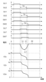
- the control device 50 when the current value of the load current is greater than the first current threshold I1, the control device 50 can discharge the resonance capacitor 9U connected in parallel to the target second switching element 2 with the load current iU without turning on the switch 8 corresponding to the target second switching element 2. This enables the power conversion device 100 to realize zero voltage soft switching of the target second switching element 2 .
- the target second switching element 2 is the second switching element 2U of the switching circuit 10U, and the control signals SU1, SU2, and SU7, the load current iU, the current i9U flowing from the resonant capacitor 9U, and the voltage V2u across the second switching element 2U are shown for the case where the current value of the load current is greater than the first current threshold I1.
- Fig. 6 also shows the dead time period Td and the additional time Tau set in the control device 50 for the control signal SU7 of the second IGBT 7U of the switch 8U.
- the control device 50 When the current value of the load current iU is greater than the first current threshold I1, the control device 50 does not set a high level period for the control signal SU7.
- the current i9U starts to flow from the resonant capacitor 9U at the start time t22 of the dead time period Td, and the current i9U drops to zero before the end time t23 of the dead time period Td, and the voltage V2u across the second switching element 2U becomes zero before the end time t23 of the dead time period Td.
- the second switching element 2U when the control signal SU2 changes from low level to high level at the end time t23 of the dead time period Td, the second switching element 2U is zero voltage soft switched.
- the control device 50 When the current value of the load current iU is smaller than the first current threshold I1, the control device 50 provides a high level period for the control signal SU7, for example, as shown by the two-dot chain line in FIG. 6.
- the start point of the high level period of the control signal SU7 at this time is, for example, the same as the start point t22 of the dead time period Td.
- the end point of the high level period of the control signal SU7 is the same as the end point t23 of the dead time period Td.
- the second switching element 2U when the control signal SU2 changes from a low level to a high level at the end point t23 of the dead time period Td, the second switching element 2U is zero-voltage soft-switched.
- the start point of the high level period of the control signal SU7 may be time t21, which is earlier than the start point of the dead time period Td by an additional time Tau.
- the end point of the high-level period of the control signal SU7 may be time t24, which is later than the end point t23 of the dead-time period Td by the additional time Tau. Note that the time before and after the period in the high-level period that overlaps with the dead-time period Td is not limited to the additional time Tau, and may be another set time.
- control signals SU1, SU2, and SU7 the load current iU, the current iL1 flowing through the resonant inductor L1, and the voltage V2u across the second switching element 2U are shown for the case where the target second switching element 2 is the second switching element 2U of the switching circuit 10U.
- FIG. 7 also illustrates the dead time period Td set in the control device 50 to prevent the first switching element 1 and the second switching element 2 of the same phase from being turned on at the same time.
- FIG. 7 also illustrates the additional time Tau set in the control device 50 for the control signal SU7 of the second IGBT 7U of the switch 8U.
- the end point of the high level period of the control signal SU7 may be the same as the end point t33 of the dead time period Td or later.
- FIG. 7 illustrates an example in which the end point of the high level period of the control signal SU7 is set to the same as the end point t33 of the dead time period Td.
- the control device 50 sets the high level period of the control signal SU7 to Tau+Td.
- the voltage V2u across the second switching element 2U becomes zero at the end point t33 of the dead time period Td.
- the current iL1 flowing through the resonant inductor L1 starts flowing at t31, the start time of the high-level period of the control signal SU7, and becomes zero at t34, the time when the additional time Tau has elapsed from t33, the end time of the dead time period Td.
- the current iL1 As for the current iL1, since iL1 ⁇ iU from t32, the start time of the dead time period Td, LC resonance occurs and a resonant current (discharge current of the resonant capacitor 9U) flows from the resonant capacitor 9U to the resonant inductor L1. After t33, the end time of the dead time period Td, the current iL1 is regenerated to the power conversion circuit 11 via the fourth diode 14, which is directly connected to the resonant inductor L1.
- the resonance half period in the case of basic operation is half the resonance period, which is the reciprocal of the resonance frequency of the resonance circuit including the resonance inductor L1 and one resonance capacitor 9. Therefore, when the inductance of the resonance inductor L1 is L and the capacitance of the resonance capacitor 9 is C, the resonance half period is ⁇ (L ⁇ C) 1/2 .
- the resonance half period in the basic operation is set to be the same as the length of the dead time period Td, for example.
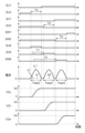
- the power conversion device 100 can charge the resonance capacitor 9U connected in series to the target first switching element 1 with the load current without the control device 50 turning on the switch 8 corresponding to the target first switching element 1. This allows the power conversion device 100 to realize zero-voltage soft switching of the target first switching element 1.
- FIG. 8 the control signals SU1, SU2, and SU6, the load current iU, the current i9U flowing from the resonant capacitor 9U, and the voltage V2u across the second switching element 2U are shown for the case where the target first switching element 1 is the first switching element 1U of the switching circuit 10U, and the current value of the load current is greater than the second current threshold I2 (in other words, the absolute value of the current value of the load current is less than the absolute value of the second current threshold I2).
- FIG. 8 also shows the dead time period Td.
- the control device 50 does not provide a high-level period for the control signal SU6.
- the current i9U starts to flow through the resonant capacitor 9U at the start time t41 of the dead time period Td.
- the resonant capacitor 9U is charged and the voltage V2u across the second switching element 2U increases, the current i9U becomes zero before the end time t23 of the dead time period Td, and the voltage V1u across the first switching element 1U becomes zero before the end time t42 of the dead time period Td.
- the control signal SU1 changes from low level to high level at the end time t42 of the dead time period Td, the first switching element 1U is zero-voltage soft-switched.
- the polarity of the resonant current is the same as the polarity of the current iL1, and in area A1, the polarity of the resonant current is positive, and in area A2, the polarity of the resonant current is negative.
- region A1 for example, during one cycle of the carrier signal, the time difference between start time t1 (see FIG. 2) of the high-level period of the control signal SU6 provided to the first IGBT 6U and start time t5 (see FIG.
- each of the multiple resonant capacitors 9U, 9V, and 9W is C
- the resonant frequency of the resonant circuit including the resonant inductor L1 will change compared to when a single-phase current flows through the resonant inductor L1, and zero-voltage soft switching may not be achieved.
- Fig. 2 is a diagram showing an example of a boundary condition between a case where the U-phase resonance current and the V-phase resonance current do not overlap (do not flow simultaneously) and a case where they overlap (flow simultaneously). The boundary condition will be described with reference to Fig. 2.
- the resonant current of the U phase and the resonant current of the V phase do not overlap, and if the time difference ⁇ Tuv is less than (Tau+Tav+Td), the resonant current of the U phase and the resonant current of the V phase overlap.
- the control device 50 sets a threshold value for the time difference ⁇ Tuv to, for example, (Tau+Tav+Td), and if the time difference ⁇ Tuv is less than the threshold value, it is estimated that resonant currents corresponding to two phases, switching circuit 10U and switching circuit 10V, of the multiple switching circuits 10, will flow simultaneously through the resonant inductor L1.
- the above threshold value settings are merely examples, and other value settings are also possible. For example, it is possible to set the threshold value to a value even greater than (Tau+Tav+Td) in consideration of the error in the additional time Tau and the error in the additional time Tav.
- the method of calculating the time difference ⁇ Tuv used to determine whether the two-phase resonant currents flow simultaneously is not limited to the above example, and other calculation methods may be used as long as they can calculate a time difference equivalent to the time difference.
- the time difference ⁇ Tuv used to determine whether the two-phase resonant currents flow simultaneously may be the time difference between the end point t2 of the high-level period of the control signal SU2 and the end point t6 of the high-level period of the control signal SV2.
- the power conversion device 100 if the time difference between the start time t3 of the high-level period of the control signal SU1 and the start time t11 of the high-level period of the control signal SW1 is (Tau+Taw+Td) or more, the resonant current of the U phase and the resonant current of the W phase do not overlap, and if the time difference is less than (Tau+Taw+Td), the resonant current of the U phase and the resonant current of the W phase overlap.
- the control device 50 sets a threshold value for the time difference to, for example, (Tau+Taw+Td), and if the time difference is less than the threshold value, it estimates that the resonant currents corresponding to two phases, the switching circuit 10U and the switching circuit 10W, among the multiple switching circuits 10, flow simultaneously through the resonant inductor L1.
- the above threshold value setting is an example, and other value settings are also possible. For example, taking into account the error in the additional time Tau and the error in the additional time Taw, the threshold value may be set to a value even greater than (Tau+Taw+Td).
- the method of calculating the time difference used to determine whether the two-phase resonant currents flow simultaneously is not limited to the above example, and other calculation methods may be used as long as they can calculate a time difference equivalent to the time difference.
- the time difference between the end point t2 of the high-level period of the control signal SU2 and the end point t10 of the high-level period of the control signal SW2 may be used as the time difference used to determine whether the two-phase resonant currents flow simultaneously.
- the V-phase resonant current and the W-phase resonant current do not overlap, and if the time difference is less than (Tav+Taw+Td), the V-phase resonant current and the W-phase resonant current overlap.
- the control device 50 sets a threshold value for the time difference to, for example, (Tav+Taw+Td), and if the time difference is less than the threshold value, it estimates that the resonant currents corresponding to two phases, the switching circuit 10V and the switching circuit 10W, of the multiple switching circuits 10, flow simultaneously through the resonant inductor L1.
- the above threshold value setting is an example, and other value settings are also possible. For example, it is possible to set the threshold value to a value even greater than (Tav+Taw+Td) in consideration of the error in the additional time Tav or the additional time Taw.
- the method of calculating the time difference used to determine whether the two-phase resonant currents flow simultaneously is not limited to the above example, and any other calculation method may be used as long as it is possible to calculate a time difference equivalent to the time difference.
- the time difference used to determine whether the two-phase resonant currents flow simultaneously may be the time difference between the end point t6 of the high-level period of the control signal SV2 and the end point t10 of the high-level period of the control signal SW2.
- control device 50 can determine whether two-phase resonant currents flow simultaneously using the same time difference and threshold value as in the case of charging operation of the resonant capacitor 9.
- the control device 50 estimates that the U-phase resonant current and the V-phase resonant current overlap.
- a threshold value e.g., Tau+Tav+Td
- the control device 50 estimates that the U-phase resonant current and the W-phase resonant current overlap.
- a threshold value e.g., Tau+Taw+Td
- the control device 50 estimates that the V-phase resonant current and the W-phase resonant current overlap.
- a threshold value e.g., Tav+Taw+Td
- the control device 50 performs shift control to shift the high-level periods of the control signals to the two switches 8, for example, so that the resonant currents passing through the two switches 8 respectively do not flow simultaneously through the resonant inductor L1.
- the control device 50 shifts the high-level periods of the control signals to the two switches 8 so that the lengths of the high-level periods of the control signals provided to the first switching element 1 and the second switching element 2 of the two switching circuits 10 corresponding to the two switches 8 do not change. For example, when shifting the high-level period of the control signal SU6 or SU7 provided to the switch 8U, the control device 50 shifts the high-level periods of the control signal SU1 and the control signal SU2, but does not change the duties of the control signal SU1 and the control signal SU2 in one period of the carrier signal.
- the control device 50 shifts the high-level periods of the control signal SV1 and the control signal SV2, but does not change the duties of the control signal SV1 and the control signal SV2 in one period of the carrier signal.
- the control device 50 shifts the high-level period of the control signal SW6 or SW7 given to the switch 8W, it shifts the high-level period of each of the control signals SW1 and SW2, but does not change the duty of each of the control signals SW1 and SW2 in one period of the carrier signal.
- the shift time of the high-level period of the control signal SU6 or SU7 to the switch 8U when shifting the high-level period of the control signal SU6 or SU7 is Tus.
- the shift time of the high-level period of the control signal SV6 or SV7 to the switch 8V when shifting the high-level period of the control signal SV6 or SV7 is Tvs.
- the shift time of the high-level period of the control signal SW6 or SW7 to the switch 8W when shifting the high-level period of the control signal SW6 or SW7 is Tws.
- control device 50 shifts the high-level periods of the control signals to the two switches 8 in different directions.
- control device 50 first compares the duties of the control signals for the two first switching elements 1 corresponding to the two switches 8 among the multiple first switching elements 1 when the polarity of the load current flowing through each of the two AC terminals 41 connected to the two switches 8 is positive.
- control device 50 shifts the high-level period of the control signal provided to the switch 8 corresponding to the first switching element 1 that provides a control signal with a relatively large duty among the two switches 8 in an earlier direction, and shifts the high-level period of the control signal provided to the switch 8 corresponding to the first switching element 1 that provides a control signal with a relatively small duty in a later direction.
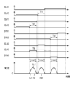
- FIG. 9 shows an example of operation when shift control is performed in a period corresponding to region A1 in FIG. 4.
- the upper part of FIG. 9 shows a timing chart of the control signals SU1, SU2, SV1, SV2, control signals SU6, SV6, load currents iU, iV, and current iL1 before the shift (when shift control is not performed) in the case where the control device 50 determines that two-phase resonant currents of U-phase and V-phase flow simultaneously.
- control device 50 shifts the start point of the high-level period of the control signal SU6 to the switch 8U by a shift time Tus, and shifts the high-level period of the control signal SV6 to the switch 8V by a shift time Tvs.
- the control device 50 sets the predetermined period to a length equal to or longer than the overlap time Tov of the two-phase resonant currents when it is determined that the two-phase resonant currents flow simultaneously.
- the overlap time Tov will be described with reference to FIG. 10.
- FIG. 10 is an explanatory diagram illustrating the waveform of the resonant current when the resonant inductor L1 is not shared (i.e., when three resonant inductors L1 are provided in one-to-one correspondence with the three resonant capacitors).
- the example in FIG. 9 shows a case where the control device 50 sets the predetermined period to Tov + ⁇ T.
- the control device 50 compares the duties of the control signals SU1, SV1 for the two first switching elements 1U, 1V that correspond one-to-one to the two switches 8U, 8V.
- the control device 50 then shifts the high-level period of the control signal SV6 provided to the switch 8V corresponding to the first switching element 1V that provides the control signal SV1 with a relatively large duty in a direction to advance by the shift time Tvs, and shifts the high-level period of the control signal SU6 provided to the switch 8U corresponding to the first switching element 1U that provides the control signal SU1 with a relatively small duty in a direction to delay by the shift time Tus.
- the control device 50 determines in advance that two-phase resonant currents, U phase and V phase, will flow simultaneously, it can perform shift control to avoid overlapping of the U phase resonant current and the V phase resonant current (see current iL1 in the lower part of Figure 9).
- the control device 50 determines that two-phase resonant currents, U phase and W phase, will flow simultaneously, it can perform shift control to avoid overlapping of the U phase resonant current and the W phase resonant current.
- the control device 50 determines that two-phase resonant currents, V phase and W phase, will flow simultaneously, it can perform shift control to avoid overlapping of the V phase resonant current and the W phase resonant current.
- the upper limit (maximum) of the shift time when the high-level period of the control signal to the switch 8 is shifted in a direction to be earlier is the shift time when the time between the start of one cycle of the carrier signal and the start of the high-level period of the shifted control signal (the control signal to the switch 8 after the shift) is set to a minimum value (e.g., 0) without changing the length of the high-level period.
- the upper limit (maximum) of the shift time when the high-level period of the control signal to the switch 8 is shifted in a direction to be later is the shift time when the time between the end of one cycle of the carrier signal and the end of the high-level period of the shifted control signal (the control signal to the switch 8 after the shift) is set to a minimum value (e.g., 0) without changing the length of the high-level period.
- the control device 50 when the control device 50 does not execute shift control, the voltages V2u and V2v across the second switching elements 2U and 2V do not rise to Vd at the time when the control signals SU1 and SV1 change from a low level period to a high level period (the end of the dead time period Td corresponding to the U phase and V phase, respectively).
- the control device 50 when the control device 50 does not execute shift control, the charging of the resonance capacitors 9U and 9V does not end at the end of the dead time period Td corresponding to the U phase and V phase, respectively.
- the shift control when the shift control is not executed, the voltages across the first switching elements 1U and 1V do not decrease to zero at the end of the dead time period Td corresponding to the U phase and V phase, respectively. As a result, in the power conversion device 100, the switching of the first switching elements 1U and 1V becomes hard switching.
- FIG. 9 shows an example of shift control when the control device 50 determines in advance that the U-phase resonant current and the V-phase resonant current will flow simultaneously through the resonant inductor L1, but this is not limiting.
- the control device 50 executes shift control even when it determines in advance that the W-phase resonant current and the U-phase resonant current will flow simultaneously through the resonant inductor L1, thereby enabling zero-voltage soft switching.
- control device 50 shifts the high-level periods of the control signals to the two switches 8 in different directions.
- control device 50 first compares the duties of the control signals for the two first switching elements 1 corresponding to the two switches 8 among the multiple first switching elements 1 when the polarity of the load current flowing through each of the two AC terminals 41 connected to the two switches 8 is negative.
- control device 50 shifts the high-level period of the control signal provided to the switch 8 corresponding to the first switching element 1 that provides a control signal with a relatively large duty in a later direction, and shifts the high-level period of the control signal provided to the switch 8 corresponding to the first switching element 1 that provides a control signal with a relatively small duty in an earlier direction.
- FIG. 11 shows an example of operation when shift control is performed in a period corresponding to region A2 in FIG. 4.
- the upper part of FIG. 11 shows a timing chart of the control signals SU1, SU2, SV1, SV2, control signals SU7, SV7, load currents iU, iV, and current iL1 before the shift (when shift control is not performed) in the case where the control device 50 determines that two-phase resonant currents of the U phase and the V phase flow simultaneously.
- control device 50 shifts the start point of the high-level period of the control signal SU7 to the switch 8U by a shift time Tus, and shifts the high-level period of the control signal SV7 to the switch 8V by a shift time Tvs.
- the control device 50 sets the predetermined period to a length equal to or longer than the overlap time Tov of the two-phase resonant currents when it is determined that the two-phase resonant currents flow simultaneously.
- the example in FIG. 11 shows a case where the control device 50 sets the predetermined period to Tov + ⁇ T.
- the control device 50 compares the duties of the control signals SU1, SV1 for the two first switching elements 1U, 1V that correspond one-to-one to the two switches 8U, 8V.
- the control device 50 then shifts the high-level period of the control signal SV7 provided to the switch 8V corresponding to the first switching element 1V that provides the control signal SV1 with a relatively large duty in a direction to delay the period by the shift time Tvs, and shifts the high-level period of the control signal SU7 provided to the switch 8U corresponding to the first switching element 1U that provides the control signal SU1 with a relatively small duty in a direction to advance the period by the shift time Tus.
- the control device 50 determines in advance that two-phase resonant currents, U-phase and V-phase, will flow simultaneously, it can perform shift control to avoid overlapping of the U-phase resonant current and the V-phase resonant current (see current iL1 in the lower part of FIG. 11).
- the control device 50 determines that two-phase resonant currents, U-phase and W-phase, will flow simultaneously, it can perform shift control to avoid overlapping of the U-phase resonant current and the W-phase resonant current.
- control device 50 determines that two-phase resonant currents, V-phase and W-phase, will flow simultaneously, it can perform shift control to avoid overlapping of the V-phase resonant current and the W-phase resonant current.
- the control device 50 when the control device 50 does not execute shift control, the voltages V1u and V1v across the first switching elements 1U and 1V do not rise to Vd at the time when the control signals SU2 and SV2 change from a low level period to a high level period (the end of the dead time period Td corresponding to the U phase and V phase, respectively).
- the discharge of the resonance capacitors 9U and 9V does not end at the end of the dead time period Td corresponding to the U phase and V phase, respectively.
- the control device 50 executes shift control, as shown in FIG. 11, the voltages V1u, V1v across the first switching elements 1U, 1V rise to Vd at the point when the control signals SU2, SV2 change from a low level period to a high level period (the end point of the dead time period Td corresponding to the U phase and V phase, respectively).
- the control device 50 executes shift control, the discharge of the resonant capacitors 9U, 9V ends at the end point of the dead time period Td corresponding to the U phase and V phase, respectively.
- the switching of the second switching elements 2U, 2V becomes zero voltage soft switching.
- FIG. 11 shows an example of shift control when the control device 50 determines in advance that the U-phase resonant current and the V-phase resonant current will flow simultaneously through the resonant inductor L1, but this is not limiting.
- the control device 50 executes shift control even when it determines in advance that the W-phase resonant current and the U-phase resonant current will flow simultaneously through the resonant inductor L1, thereby enabling zero-voltage soft switching.
- the control device 50 determines that a resonant current passing through each of two of the multiple switches 8 flows simultaneously through the resonant inductor L1
- the control device 50 performs control to shift the high-level period of the control signal to each of the two switches 8 so that the resonant current passing through each of the two switches 8 does not flow simultaneously through the resonant inductor L1. This enables the power conversion device 100 to more reliably achieve soft switching.
- the control device 50 when performing shift control, shifts the high-level period of the control signal to each of the two switches 8 so that the length of the high-level period of the control signal provided to each of the first switching element 1 and the second switching element 2 of the switching circuit 10 connected to the two switches 8 among the multiple switching circuits 10 does not change. This makes it possible for the power conversion device 100 according to the first embodiment to suppress changes in the line voltage.
- the control device 50 when performing shift control, shifts the high-level periods of the control signals to the two switches 8 in different directions. This allows the power conversion device 100 according to the first embodiment to achieve a higher frequency.
- the control device 50 compares the duties of the control signals for the two first switching elements 1 corresponding to the two switches 8. The control device 50 then shifts the high-level period of the control signal given to the switch 8 corresponding to the first switching element 1 that gives a control signal with a relatively large duty in an earlier direction, and shifts the high-level period of the control signal given to the switch 8 corresponding to the first switching element 1 that gives a control signal with a relatively small duty in a later direction.
- the control device 50 also compares the duties of the control signals for the two first switching elements 1 corresponding to the two switches 8 when the polarity of the load current flowing through each of the two AC terminals 41 connected to the two switches 8 is negative. The control device 50 then shifts the high-level period of the control signal provided to the switch 8 corresponding to the first switching element 1 that provides a control signal with a relatively large duty in a later direction, and shifts the high-level period of the control signal provided to the switch 8 corresponding to the first switching element 1 that provides a control signal with a relatively small duty in an earlier direction. This allows the power conversion device 100 according to the first embodiment to achieve a higher frequency.
- the operation of the shift control of the control device 50 when it is determined that the two-phase resonant currents overlap differs from the operation of the control device 50 according to the first embodiment.
- control device 50 for soft switching the first switching element 1 in the case where the control device 50 determines that two-phase resonant currents flow simultaneously through the resonant inductor L1 will be explained with reference to Figs. 12 and 13, and the operation of the control device 50 for soft switching the second switching element 2 will be explained with reference to Fig. 14.
- control device 50 shifts the high-level periods of the control signals to the two switches 8 in different directions.
- control device 50 first compares the duties of the control signals for the two first switching elements 1 corresponding to the two switches 8 among the multiple first switching elements 1 when the polarity of the load current flowing through each of the two AC terminals 41 connected to the two switches 8 is positive.
- control device 50 shifts the high-level period of the control signal provided to the switch 8 corresponding to the first switching element 1 that provides a control signal with a relatively large duty in a later direction, and shifts the high-level period of the control signal provided to the switch 8 corresponding to the first switching element 1 that provides a control signal with a relatively small duty in an earlier direction.
- FIG. 12 shows an example of operation when shift control is performed in a period corresponding to region A1 in FIG. 4.
- the upper part of FIG. 12 shows a timing chart of the control signals SU1, SU2, SV1, SV2, control signals SU6, SV6, load currents iU, iV, and current iL1 before the shift (when shift control is not performed) in the case where the control device 50 determines that two-phase resonant currents of U-phase and V-phase flow simultaneously.
- control device 50 shifts the start point of the high-level period of the control signal SU6 to the switch 8U by a shift time Tus, and shifts the high-level period of the control signal SV6 to the switch 8V by a shift time Tvs.
- the control device 50 sets the predetermined period to ⁇ Tuv+Ti+ ⁇ T, where Ti is the resonant current time and ⁇ T is the time margin.
- Ta is the additional time during the high level period of the switch 8 connected to the AC terminal 41 having the larger absolute value of the load current of the two switches 8, and the resonant current time Ti is calculated by the formula 2 ⁇ Ta+Tres/2.
- Figure 12 illustrates the resonant current time Tiu of the U phase and the resonant current time Tiv of the V phase.
- FIG. 12 shows a case where the U-phase resonant current and the V-phase resonant current overlap, but the method of determining the specified period and the method of determining the shift direction of the control signal are similar in both cases where the U-phase resonant current and the W-phase resonant current overlap, and where the V-phase resonant current and the W-phase resonant current overlap.
- the example in FIG. 12 shows a case where the control device 50 sets the predetermined period to ⁇ Tuv + (2 ⁇ Tav + Tres/2) + ⁇ T.
- the control device 50 sets the predetermined period to ⁇ Tuv + (2 ⁇ Tav + Tres/2) + ⁇ T.
- the control device 50 compares the duties of the control signals SU1, SV1 for the two first switching elements 1U, 1V that correspond one-to-one to the two switches 8U, 8V.
- the control device 50 then shifts the high-level period of the control signal SV6 provided to the switch 8V corresponding to the first switching element 1V that provides the control signal SV1 with a relatively large duty in a direction to delay the period by the shift time Tvs, and shifts the high-level period of the control signal SU6 provided to the switch 8U corresponding to the first switching element 1U that provides the control signal SU1 with a relatively small duty in a direction to advance the period by the shift time Tus.
- the control device 50 determines in advance that two-phase resonant currents, U phase and V phase, will flow simultaneously, it can perform shift control to avoid overlapping of the U phase resonant current and the V phase resonant current (see current iL1 in the lower part of Figure 12).
- the control device 50 determines that two-phase resonant currents, U phase and W phase, will flow simultaneously, it can perform shift control to avoid overlapping of the U phase resonant current and the W phase resonant current.
- the control device 50 determines that two-phase resonant currents, V phase and W phase, will flow simultaneously, it can perform shift control to avoid overlapping of the V phase resonant current and the W phase resonant current.
- the upper limit (maximum) of the shift time when the high-level period of the control signal to the switch 8 is shifted in a later direction is the shift time when the time between the end of one cycle of the carrier signal and the end of the high-level period of the shifted control signal (the control signal to the switch 8 after the shift) is set to 0.
- the upper limit (maximum) of the shift time when the high-level period of the control signal to the switch 8 is shifted in an earlier direction is the shift time when the time between the start of one cycle of the carrier signal and the start of the high-level period of the shifted control signal (the control signal to the switch 8 after the shift) is set to 0.
- the control device 50 determines that two-phase resonant currents flow simultaneously through the resonant inductor L1 and executes shift control, as shown in FIG. 12, overlap of the resonant currents is avoided, and charging of the resonant capacitors 9U and 9V ends at the end of the dead time periods Td corresponding to the U and V phases, respectively. Therefore, in the power conversion device 100, when the control device 50 executes shift control, the switching of the first switching elements 1U and 1V becomes zero-voltage soft switching.
- FIG. 12 shows an example of shift control when the control device 50 determines in advance that the U-phase resonant current and the V-phase resonant current will flow simultaneously through the resonant inductor L1, but this is not limiting.
- the control device 50 executes shift control even when it determines in advance that the W-phase resonant current and the U-phase resonant current will flow simultaneously through the resonant inductor L1, thereby enabling zero-voltage soft switching.
- control device 50 shifts the high-level periods of the control signals to the two switches 8 in different directions.
- control device 50 first compares the duties of the control signals for the two first switching elements 1 corresponding to the two switches 8 among the multiple first switching elements 1 when the polarity of the load current flowing through each of the two AC terminals 41 connected to the two switches 8 is negative.
- control device 50 shifts the high-level period of the control signal provided to the switch 8 corresponding to the first switching element 1 that provides a control signal with a relatively large duty among the two switches 8 in an earlier direction, and shifts the high-level period of the control signal provided to the switch 8 corresponding to the first switching element 1 that provides a control signal with a relatively small duty in a later direction.
- FIG. 14 shows an example of operation when shift control is performed in the period corresponding to region A2 in FIG. 4.
- the upper part of FIG. 14 shows a timing chart of the control signals SU1, SU2, SV1, SV2, control signals SU7, SV7, load currents iU, iV, and current iL1 before the shift (when shift control is not performed) in the case where the control device 50 judges that two-phase resonant currents of the U phase and the V phase flow simultaneously.
- control device 50 shifts the start point of the high-level period of the control signal SU7 to the switch 8U by a shift time Tus, and shifts the high-level period of the control signal SV7 to the switch 8V by a shift time Tvs.
- control device 50 sets the predetermined period to ⁇ Tuv + (2 ⁇ Tau + Tres/2) + ⁇ T.
- the control device 50 compares the duties of the control signals SU1, SV1 for the two first switching elements 1U, 1V that correspond one-to-one to the two switches 8U, 8V.
- the control device 50 then shifts the high-level period of the control signal SV7 provided to the switch 8V corresponding to the first switching element 1V that provides the control signal SV1 with a relatively large duty in a direction to advance by the shift time Tvs, and shifts the high-level period of the control signal SU7 provided to the switch 8U corresponding to the first switching element 1U that provides the control signal SU1 with a relatively small duty in a direction to delay by the shift time Tus.
- the control device 50 determines in advance that two-phase resonant currents, U-phase and V-phase, will flow simultaneously, it can perform shift control to avoid overlapping of the U-phase resonant current and the V-phase resonant current (see current iL1 in the lower part of FIG. 14).
- the control device 50 determines that two-phase resonant currents, U-phase and W-phase, will flow simultaneously, it can perform shift control to avoid overlapping of the U-phase resonant current and the W-phase resonant current.
- control device 50 determines that two-phase resonant currents, V-phase and W-phase, will flow simultaneously, it can perform shift control to avoid overlapping of the V-phase resonant current and the W-phase resonant current.
- the discharge of the resonant capacitors 9U, 9V ends at the point when the control signals SU2, SV2 change from a low level period to a high level period (the end point of the dead time period Td corresponding to the U phase and V phase, respectively). Therefore, in the power conversion device 100, when the control device 50 executes shift control, the switching of the second switching elements 2U, 2V becomes zero voltage soft switching.
- FIG. 14 shows an example of shift control when the control device 50 determines in advance that the U-phase resonant current and the V-phase resonant current will flow simultaneously through the resonant inductor L1, but this is not limiting.
- the control device 50 executes shift control even when it determines in advance that the W-phase resonant current and the U-phase resonant current will flow simultaneously through the resonant inductor L1, thereby enabling zero-voltage soft switching.
- the control device 50 is configured to combine the shift control of the control device 50 according to the second embodiment with the shift control of the control device 50 according to the first embodiment, and to execute the shift control of the control device 50 according to the second embodiment and the shift control of the control device 50 according to the first embodiment alternately or at an arbitrary ratio.
- the power conversion device 100 according to the modification can reduce the bias of the fluctuation of the ripple of the line voltage compared to the power conversion device 100 according to the first embodiment and the power conversion device 100 according to the second embodiment.
- the power conversion device 100 according to the modification it is possible to distribute the period during which the resonant current flows through the resonant inductor L1 compared to the power conversion device 100 according to the first embodiment and the power conversion device 100 according to the second embodiment, and it is possible to reduce the thermal burden on the resonant inductor L1.
- the shift control operation that the control device 50 executes when it determines that the three-phase resonant currents overlap differs from the shift control operation of the control device 50 according to the first embodiment.
- control device 50 executes shift control when it is determined that a resonant current flows through each of three of the multiple switches 8 simultaneously in the resonant inductor L1.
- shift control when it is determined that a resonant current flows through each of three of the multiple switches 8 simultaneously in the resonant inductor L1.
- the control device 50 determines that "three-phase resonant currents flow simultaneously" when, for example, the rotation speed of the motor (e.g., the number of rotations [rpm]) falls below a rotation speed threshold.
- control device 50 determines that "three-phase resonant currents flow simultaneously" when, for example, the rotation speed calculated from sensor information output from a sensor device (e.g., an encoder or resolver) for detecting the rotation speed of the motor, or the estimated rotation speed, falls below the rotation speed threshold.
- a sensor device e.g., an encoder or resolver
- each of the multiple resonant capacitors 9U, 9V, and 9W is C
- the resonant frequency of the resonant circuit including the resonant inductor L1 will change compared to when a single-phase current flows through the resonant inductor L1, and zero-voltage soft switching may not be achieved.
- control device 50 determines that the resonant currents passing through the three switches 8 flow simultaneously through the resonant inductor L1, it performs shift control to shift the high-level periods of the control signals to two of the three switches 8 so that the resonant currents passing through the three switches 8 do not flow simultaneously through the resonant inductor L1.
- control device 50 shifts the high-level period of the control signal to the two switches 8 so that the length of the high-level period of the control signal provided to each of the first switching element 1 and the second switching element 2 of the switching circuit 10 connected to the two switches 8 among the multiple switching circuits 10 does not change.
- control device 50 When performing shift control, the control device 50 shifts the control signals to any two of the three switches 8, and shifts the high-level periods of the two switches 8 to different directions so that the resonant currents passing through the three switches 8 do not flow simultaneously through the resonant inductor L1.
- FIG. 15 shows a timing chart of the power conversion device 100 when the control device 50 executes shift control in a case where the control device 50 determines that three-phase resonant currents of the U phase, the V phase, and the W phase flow simultaneously when the polarity of the current iL1 is positive
- Fig. 16 shows a timing chart of the power conversion device 100 when the control device 50 does not execute shift control. Note that Figs. 15 and 16 show timing charts for a part of a period within one cycle of the carrier signal.
- the control device 50 shifts the control signals SU6 and SW6 to the two switches 8U and 8W, respectively, but this is not limited thereto.
- the control device 50 shifts the high-level period of the control signal SU6 to the switch 8U by a first shift time T1 in a direction to advance the start point of the high-level period of the control signal SU6 to the switch 8U so that overlapping of resonant currents does not occur in a combination of one of the two switches 8 to be shifted and one switch 8 that is not to be shifted (here, the U-phase resonant current and the V-phase resonant current do not flow simultaneously).
- control device 50 shifts the high-level period of the control signal SW6 to the switch 8W by a second shift time T2 in a direction to delay the start point of the high-level period of the control signal SW6 to the switch 8W so that overlapping of resonant currents does not occur in a combination of the remaining one of the two switches 8 to be shifted and the other two switches 8 (here, the W-phase resonant current does not flow simultaneously with both the U-phase resonant current and the V-phase resonant current).
- the state before the high-level period of the control signals SU6 and SW6 is shifted i.e., the state in FIG. 16
- the state after the shift is shown by a solid line.
- the high-level period of the control signal SU6 to the switch 8U is shifted by the first shift time T1 in a direction to advance the start point of the high-level period of the control signal SU6 to the switch 8U, and the high-level period of the control signal SW6 to the switch 8W is shifted by the second shift time T2 in a direction to delay the start point of the high-level period of the control signal SW6 to the switch 8W, but this is not limited to this.
- the high-level period of the control signal SW6 to the switch 8W may be shifted by the first shift time T1 in a direction to advance the start point of the high-level period of the control signal SW6 to the switch 8W, and the high-level period of the control signal SU6 to the switch 8U may be shifted by the second shift time T2 in a direction to delay the start point of the high-level period of the control signal SU6 to the switch 8U.
- the combination of the two switches 8 to be shifted is not limited to the combination of switches 8U and 8W, but may be the combination of switches 8U and 8V, or the combination of switches 8V and 8W.
- the first shift time T1 and the second shift time T2 are each a predetermined period.
- the upper limit (maximum) of the first shift time T1 when the high-level period of the control signal to the switch 8 is shifted in a direction to be advanced is the shift time when the time between the start of one cycle of the carrier signal and the start of the high-level period of the shifted control signal (the control signal to the switch 8 after the shift) is set to a minimum value (e.g., 0) without changing the length of the high-level period.
- the upper limit (maximum) of the second shift time T2 when the high-level period of the control signal to the switch 8 is shifted in a direction to be delayed is the shift time when the time between the end of one cycle of the carrier signal and the end of the high-level period of the shifted control signal (the control signal to the switch 8 after the shift) is set to a minimum value (e.g., 0) without changing the length of the high-level period.
- the voltages V2u, V2v, and V2w across the second switching elements 2U, 2V, and 2W do not rise to Vd at the time when the control signals SU1, SV1, and SW1 change from a low level period to a high level period (at the end of the dead time period Td corresponding to the U phase, V phase, and W phase, respectively).
- the control device 50 when the control device 50 does not execute the shift control, the charging of the resonance capacitors 9U, 9V, and 9W does not end at the end of the dead time period Td corresponding to the U phase, V phase, and W phase, respectively.
- the control device 50 when the control device 50 does not execute the shift operation, the voltages across the first switching elements 1U, 1V, and 1W do not decrease to zero at the end of the dead time period Td corresponding to the U phase, V phase, and W phase, respectively, and the switching of the first switching elements 1U, 1V, and 1W becomes hard switching.
- the voltages V2u, V2v, and V2w across the second switching elements 2U, 2V, and 2W rise to Vd at the time when the control signals SU1, SV1, and SW1 change from a low-level period to a high-level period (the end of the dead time period Td corresponding to the U phase, V phase, and W phase, respectively).
- the control device 50 executes shift control, charging of the resonance capacitors 9U, 9V, and 9W ends at the end of the dead time period Td corresponding to the U phase, V phase, and W phase, respectively. Therefore, in the power conversion device 100, when the control device 50 executes shift control, the switching of the first switching elements 1U, 1V, and 1W becomes zero-voltage soft switching.
- the temporal relationship between the control signals to the first switching element 1 and the relationship between the control signals to the second switching element 2 are not limited.
- the start point of the high-level period of the control signal SV6 may be earlier than the start point of the high-level period of the control signal SU6, and the start point of the control signal SU6 may be earlier than the start point of the control signal SW6.
- FIG. 17 shows a timing chart of the power conversion device 100 when the control device 50 executes shift control in a case where the control device 50 determines that three-phase resonant currents of the U phase, the V phase, and the W phase flow simultaneously when the polarity of the current iL1 is negative
- Fig. 18 shows a timing chart of the power conversion device 100 when the control device 50 does not execute shift control. Note that Figs. 17 and 18 show timing charts for a part of a period within one cycle of the carrier signal.
- a timing chart is shown of the control signals SU1, SU2, SV1, SV2, SW1, SW2, SU7, SV7, SW7, the load currents iU, iV, the current iL1, and the voltages V2u, V2v, and V2w across the second switching elements 2U, 2V, and 2W.
- the control device 50 shifts the control signals SU7 and SW7 to the two switches 8U and 8W, respectively, but this is not limited to this.
- the control device 50 shifts the start point of the high-level period of the control signal SU7 to the switch 8U by a first shift time T1 in a direction to advance the start point of the high-level period of the control signal SU7 to the switch 8U so that overlapping of resonant currents does not occur in a combination of one of the two switches 8 to be shifted and one switch 8 that is not to be shifted (here, the U-phase resonant current and the V-phase resonant current do not flow simultaneously).
- control device 50 shifts the start point of the high-level period of the control signal SW7 to the switch 8W by a second shift time T2 in a direction to delay the start point of the high-level period of the control signal SW7 to the switch 8W so that overlapping of resonant currents does not occur in a combination of the remaining one of the two switches 8 to be shifted and the other two switches 8 (here, the W-phase resonant current does not flow simultaneously with both the U-phase resonant current and the V-phase resonant current).
- FIG. 17 the state before the high-level period of the control signals SU7 and SW7 is shifted (i.e., the state in FIG. 18) is shown by a two-dot chain line, and the state after the shift is shown by a solid line.
- the high level period of the control signal SU7 to the switch 8U is shifted by the first shift time T1 in a direction to advance the start point of the high level period of the control signal SU7 to the switch 8U, and the high level period of the control signal SW7 to the switch 8W is shifted by the second shift time T2 in a direction to delay the start point of the high level period of the control signal SW7 to the switch 8W, but this is not limited to the above.
- the high-level period of the control signal SW7 to the switch 8W may be shifted by a first shift time T1 in a direction to advance the start point of the high-level period of the control signal SW7, and the high-level period of the control signal SU7 to the switch 8U may be shifted by a second shift time T2 in a direction to delay the start point of the high-level period of the control signal SU7 to the switch 8U.
- the combination of the two switches 8 to be shifted is not limited to the combination of switches 8U and 8W, but may be the combination of switches 8U and 8V, or the combination of switches 8V and 8W.
- the voltages V2u, V2v, and V2w across the second switching elements 2U, 2V, and 2W do not drop to zero at the time when the control signals SU2, SV2, and SW2 change from a low level period to a high level period (the end of the dead time period Td corresponding to the U phase, V phase, and W phase, respectively).
- the discharge of the resonance capacitors 9U, 9V, and 9W does not end at the end of the dead time period Td corresponding to the U phase, V phase, and W phase, respectively.
- the control device 50 when the control device 50 does not execute the shift operation, the voltages across the second switching elements 2U, 2V, and 2W do not drop to zero at the end of the dead time period Td corresponding to the U phase, V phase, and W phase, respectively, and the switching of the second switching elements 2U, 2V, and 2W becomes hard switching.
- the voltages V2u, V2v, and V2w across the second switching elements 2U, 2V, and 2W decrease to zero at the time when the control signals SU2, SV2, and SW2 change from a low-level period to a high-level period (the end of the dead time period Td corresponding to the U phase, V phase, and W phase, respectively).
- the control device 50 executes shift control
- the discharge of the resonance capacitors 9U, 9V, and 9W ends at the end of the dead time period Td corresponding to the U phase, V phase, and W phase, respectively. Therefore, in the power conversion device 100, when the control device 50 executes shift control, the switching of the second switching elements 2U, 2V, and 2W becomes zero-voltage soft switching.
- the control device 50 determines that the resonant currents passing through the three switches 8 flow simultaneously through the resonant inductor L1
- the control device 50 performs control to shift the high-level periods of the control signals to two of the three switches 8 so that the resonant currents passing through the three switches 8 do not flow simultaneously through the resonant inductor L1. This enables the power conversion device 100 to more reliably achieve soft switching.
- the shift control operation that the control device 50 executes when it determines that the three-phase resonant currents overlap differs from the shift control operation of the control device 50 according to the third embodiment.
- control device 50 executes shift control when it is determined that a resonant current flows through each of three of the multiple switches 8 simultaneously in the resonant inductor L1.
- the control device 50 shifts the high-level period of the control signal to the two switches 8 so that the length of the high-level period of the control signal provided to each of the first switching element 1 and the second switching element 2 of the switching circuit 10 connected to the two switches 8 among the multiple switching circuits 10 does not change.
- the control device 50 when performing shift control, shifts the control signals to any two of the three switches 8, and shifts the high-level periods of the two switches 8 to be shifted in the same direction so that the resonant currents passing through the three switches 8 do not flow simultaneously through the resonant inductor L1.
- FIG. 19 shows a timing chart of the power conversion device 100 when the control device 50 executes shift control in a case where the control device 50 determines that three-phase resonant currents of the U, V, and W phases flow simultaneously when the polarity of the current iL1 is positive
- FIG. 16 described in embodiment 3 shows a timing chart of the power conversion device 100 when the control device 50 does not execute shift control. Note that FIG. 19 illustrates a timing chart for a portion of one period of the carrier signal.
- FIG. 19 illustrates a timing chart of the control signals SU1, SU2, SV1, SV2, SW1, SW2, SU6, SV6, SW6, load currents iU, iV, current iL1, and voltages V2u, V2v, V2w across the second switching elements 2U, 2V, 2W.
- the control device 50 shifts the control signals SV6 and SW6 to the two switches 8V and 8W, respectively, but this is not limited to this.
- the control device 50 shifts the high-level period of the control signal SV6 to the switch 8V by a first shift time T1 in a direction to delay the start point of the high-level period of the control signal SV6 to the switch 8V so that overlap of the resonant current does not occur in a combination of one of the two switches 8 to be shifted and one switch 8 that is not to be shifted (here, the U-phase resonant current and the V-phase resonant current do not flow simultaneously).
- control device 50 shifts the high-level period of the control signal SW6 to the switch 8W by a second shift time T2 in a direction to delay the start point of the high-level period of the control signal SW6 to the switch 8W so that overlap of the resonant current does not occur in a combination of the remaining one of the two switches 8 to be shifted and the other two switches 8 (here, the W-phase resonant current does not flow simultaneously with both the U-phase resonant current and the V-phase resonant current).
- FIG. 19 the state before the high-level period of the control signals SV6 and SW6 is shifted (i.e., the state in FIG. 16) is shown by a two-dot chain line, and the state after the shift is shown by a solid line.
- the voltages V2u, V2v, and V2w across the second switching elements 2U, 2V, and 2W increase to Vd at the time when the control signals SU1, SV1, and SW1 change from a low level period to a high level period (the end of the dead time period Td corresponding to the U phase, V phase, and W phase, respectively).
- the control device 50 executes the shift control
- the charging of the resonance capacitors 9U, 9V, and 9W ends at the end of the dead time period Td corresponding to the U phase, V phase, and W phase, respectively. Therefore, in the power conversion device 100, when the control device 50 executes the shift control, the switching of the first switching elements 1U, 1V, and 1W becomes zero-voltage soft switching.
- the control device 50 determines that the resonant currents passing through the three switches 8 flow simultaneously through the resonant inductor L1
- the control device 50 performs control to shift the high-level period of the control signals to two of the three switches 8 so that the resonant currents passing through the three switches 8 do not flow simultaneously through the resonant inductor L1. This enables the power conversion device 100 to more reliably achieve soft switching.
- the high level period of the control signal SV6 to the switch 8V is shifted by the first shift time T1 in a direction to delay the start point of the high level period of the control signal SV6, and the high level period of the control signal SW6 to the switch 8W is shifted by the second shift time T2 in a direction to delay the start point of the high level period of the control signal SW6, but this is not limited to this.
- the high level period of the control signal SW6 to the switch 8W may be shifted by the first shift time T1 in a direction to delay the start point of the high level period of the control signal SW6, and the control signal SV6 to the switch 8V may be shifted by the second shift time T2 in a direction to delay the start point of the high level period of the control signal SV6.
- the combination of the two switches 8 to be shifted is not limited to the combination of switches 8V and 8W, but may be the combination of switches 8U and 8V, or may be the combination of switches 8U and 8W.
- the shift direction is not limited to the direction to delay the high level period of the control signals of the two switches 8, but may be the direction to advance the high level period of the control signals of the two switches 8.
- the second shift time T2 is longer than the first shift time T1, but this is not limited thereto, and the first shift time T1 may be longer than the second shift time.
- FIG. 19 describes the operation for soft switching the first switching elements 1U, 1V, and 1W
- the shift control operation is similar when soft switching the second switching elements 2U, 2V, and 2W.
- the control device 50 appropriately changes the combination of the two switches 8 that are the targets of the shift control, for example, it is possible to reduce the bias of the fluctuation of the ripple of the line voltage.
- the shift control operation that the control device 50 executes when it determines that the three-phase resonant currents overlap is different from the shift control operation of the control device 50 according to the third embodiment.
- the control device 50 executes shift control so that the resonant currents do not overlap in the combination of one switch 8 of the three switches 8 and each of the remaining two switches 8.
- the control device 50 determines that resonant currents passing through the three switches 8 simultaneously flow through the resonant inductor L1
- the control device 50 performs a first shift control as the shift control when a first condition is satisfied
- the control device 50 performs a second shift control as the shift control when a second condition is satisfied.
- the first condition is that the time difference between the start points of the high-level periods of the control signals SU1, SV1, and SW1 having the longest high-level period and the control signal having the shortest high-level period given to the three first switching elements 1 is longer than the resonance half period Tres.
- the resonance half period Tres is half the value of the resonance period determined by the reciprocal of the resonance frequency of the resonance circuit including the resonance inductor L1 and one of the multiple resonance capacitors 9.
- the first shift control includes control to shift the high-level period of the control signal to the switch 8 corresponding to the first switching element 1 that gives the control signal having the second longest high-level period among the control signals SU1, SV1, and SW1 given to the three first switching elements 1.
- the second condition is that the time difference between the start points of the high-level periods of the control signals SU2, SV2, and SW2 having the longest high-level period and the control signal having the shortest high-level period given to the three second switching elements 2 is longer than the resonance half period Tres.
- the second shift control includes control to shift the high-level period of the control signal to the switch 8 corresponding to the second switching element 2 that provides the control signal having the second longest high-level period among the control signals SU2, SV2, SW2 provided to each of the three second switching elements 2.
- shift control first shift control or second shift control
- the control device 50 shifts the high-level period of the control signal to the switch 8 so that the length of the high-level period of the control signal does not change.
- FIG. 20 shows a timing chart of the power conversion device 100 when the control device 50 executes the first shift control in a charging operation for charging a plurality of resonant capacitors 9 when the control device 50 determines that resonant currents flow simultaneously through each of the three switches 8, and
- FIG. 21 shows a timing chart of the power conversion device 100 when the control device 50 does not execute the first shift control. Note that FIGS. 20 and 21 show timing charts for a portion of one period of the carrier signal.
- the control device 50 shifts the high level period of the control signal SV6 to the switch 8V corresponding to the first switching element 1V that provides the control signal SV1 by shift time Ts in the direction of advancing it.
- the shift time Ts is a predetermined period.
- the state before the high level period is shifted i.e., the state in Figure 21
- the state after the shift is shown by a solid line.
- the control device 50 shifts the high-level period of the control signal SV6 to the switch 8V by a shift time Ts in a direction to advance the start point of the high-level period of the control signal SV6 to the switch 8V so that the resonant current flowing through the switch 8V and the resonant current flowing through the switch 8U do not flow simultaneously through the resonant inductor L1, and the resonant current flowing through the switch 8V and the resonant current flowing through the switch 8W do not flow simultaneously through the resonant inductor L1.
- the length of the predetermined period (shift time Ts) is, for example, 2 ⁇ Tres/2.
- the length of the predetermined period is not limited to this, and may be any length that can avoid overlapping of the resonant currents.
- the direction in which the high-level period of the control signal SV6 is shifted is not limited to the direction of advancing the high-level period, and may be the direction of delaying the high-level period.
- the control device 50 when the control device 50 executes shift control, the voltages V2u, V2v, and V2w across the second switching elements 2U, 2V, and 2W increase to Vd at the time when the control signals SU1, SV1, and SW1 change from a low-level period to a high-level period (the end of the dead time period Td corresponding to the U phase, V phase, and W phase, respectively).
- the control device 50 executes shift control in the power conversion device 100
- the charging of the resonant capacitors 9U, 9V, and 9W ends at the end of the dead time period Td corresponding to the U phase, V phase, and W phase, respectively. Therefore, in the power conversion device 100, when the control device 50 executes shift control, the switching of the first switching elements 1U, 1V, and 1W becomes zero-voltage soft switching.
- the control device 50 when the second condition is satisfied, performs the second shift control, thereby enabling the second switching elements 2U, 2V, and 2W to be zero-voltage soft-switched.
- the power conversion device 100 according to embodiment 5 can perform soft switching more reliably.
- FIG. 6 A power conversion device 100A according to the sixth embodiment will be described with reference to Fig. 22.
- components similar to those of the power conversion device 100 according to the first embodiment will be denoted by the same reference numerals and description thereof will be omitted.
- the first IGBT 6 and the second IGBT 7 are connected in anti-series in each of the multiple switches 8.
- the collector terminal of the first IGBT 6 and the collector terminal of the second IGBT 7 are connected in each of the multiple switches 8, the emitter terminal of the first IGBT 6 is connected to the connection point 3 of a corresponding one of the multiple switching circuits 10, and the emitter terminal of the second IGBT 7 is connected to the common connection point 25.
- Each of the multiple switches 8 further includes a diode 61 connected in anti-parallel to the first IGBT 6 and a diode 71 connected in anti-parallel to the second IGBT 7.
- each of the first IGBT 6 and the second IGBT 7 may be replaced with a MOSFET or a bipolar transistor.
- the diodes 61 and 71 in FIG. 22 may be replaced with a parasitic diode of the replaced element, or an element built into the chip of the replaced element.
- the diodes 61 and 71 are not limited to being externally attached to the first IGBT 6 and the second IGBT 7, but may also be elements built into the chip.
- control device 50 is, for example, the same as the operation of the control device 50 in embodiment 1, but is not limited thereto, and may be the same as the operation of the control device 50 in any of embodiments 2 to 5, or may execute the shift control of the control device 50 in embodiments 1 to 5.
- FIG. 7 A power conversion device 100A according to the seventh embodiment will be described with reference to Fig. 23.
- components similar to those of the power conversion device 100 according to the first embodiment will be denoted by the same reference numerals and will not be described.
- the first IGBT 6 and the second IGBT 7 are connected in anti-series in each of the multiple switches 8.
- the emitter terminal of the first IGBT 6 and the emitter terminal of the second IGBT 7 are connected in each of the multiple switches 8, the collector terminal of the second IGBT 7 is connected to the connection point 3 of a corresponding one of the multiple switching circuits 10, and the collector terminal of the first IGBT 6 is connected to the common connection point 25.
- Each of the multiple switches 8 further includes a diode 61 connected in anti-parallel to the first IGBT 6 and a diode 71 connected in anti-parallel to the second IGBT 7.
- each of the first IGBT 6 and the second IGBT 7 may be replaced with a MOSFET or a bipolar transistor.
- the diodes 61 and 71 in FIG. 23 may be replaced with a parasitic diode of the replaced element, or an element built into the chip of the replaced element.
- the diodes 61 and 71 are not limited to being externally attached to the first IGBT 6 and the second IGBT 7, but may also be elements built into the chip.
- control device 50 is, for example, the same as the operation of the control device 50 in embodiment 1, but is not limited thereto, and may be the same as the operation of the control device 50 in any of embodiments 2 to 5, or may execute the shift control of the control device 50 in embodiments 1 to 5.
- FIG. 8 A power conversion device 100A according to an eighth embodiment will be described with reference to Fig. 24.
- components similar to those of the power conversion device 100 according to the first embodiment will be denoted by the same reference numerals and will not be described.
- the first MOSFET 6A and the second MOSFET 7A are connected in anti-series in each of the multiple switches 8.
- the drain terminal of the first MOSFET 6A and the drain terminal of the second MOSFET 7A are connected in anti-parallel in each of the multiple switches 8.
- Each of the multiple switches 8 further includes a diode 61 connected in anti-parallel to the first MOSFET 6A and a diode 71 connected in anti-parallel to the second MOSFET 7A.
- the source terminal of the second MOSFET 7A is connected to the common connection point 25.
- the source terminal of the first MOSFET 6A is connected to the connection point 3 of the switching circuit 10 corresponding to the switch 8 having the first MOSFET 6A.
- the first MOSFET 6A and the second MOSFET 7A of the switch 8U are provided with control signals SU6 and SU7 from the control device 50.
- the first MOSFET 6A and the second MOSFET 7A of the switch 8V are provided with control signals SV6 and SV7 from the control device 50.
- the first MOSFET 6A and the second MOSFET 7A of the switch 8W are provided with control signals SW6 and SW7 from the control device 50.
- control device 50 is, for example, similar to the operation of the control device 50 of embodiment 1, but is not limited thereto, and may be similar to the operation of the control device 50 of any of embodiments 2 to 5, or may execute the shift control of the control device 50 of embodiments 1 to 5.
- FIG. 9 A power conversion device 100A according to the ninth embodiment will be described with reference to Fig. 25.
- components similar to those of the power conversion device 100 according to the first embodiment are denoted by the same reference numerals and descriptions thereof will be omitted.
- a diode 63 is connected in series to the first MOSFET 6A, and a diode 73 is connected in series to the second MOSFET 7A.
- the series circuit of the first MOSFET 6A and the diode 63 and the series circuit of the second MOSFET 7A and the diode 73 are connected in anti-parallel.
- control device 50 is, for example, similar to the operation of the control device 50 of embodiment 1, but is not limited thereto, and may be similar to the operation of the control device 50 of any of embodiments 2 to 5, or may execute the shift control of the control device 50 of embodiments 1 to 5.
- FIG. 26 A power conversion device 100A according to the tenth embodiment will be described with reference to Fig. 26.
- components similar to those of the power conversion device 100 according to the first embodiment will be denoted by the same reference numerals and description thereof will be omitted.
- each of the multiple switches 8 has one MOSFET 80, a diode 83 connected in anti-parallel to the MOSFET 80, a series circuit of two diodes 84 and 85 connected in anti-parallel to the MOSFET 80, and a series circuit of two diodes 86 and 87 connected in anti-parallel to the MOSFET 80.
- connection point between the diode 84 and the diode 85 in the switch 8 (the first end of the switch 8) is connected to the connection point 3 of the corresponding switching circuit 10 among the multiple switching circuits 10, and the connection point between the diode 86 and the diode 87 (the second end of the switch 8) is connected to the common connection point 25.
- the switch 8 when the MOSFET 80 is in the on state, the switch 8 is in the on state, and when the MOSFET 80 is in the off state, the switch 8 is in the off state.
- the MOSFETs 80 of the multiple switches 8 are controlled by the control device 50.
- the control device 50 outputs a control signal SU8 that controls the on/off state of the MOSFET 80 of the switch 8U, a control signal SV8 that controls the on/off state of the MOSFET 80 of the switch 8V, and a control signal SW8 that controls the on/off state of the MOSFET 80 of the switch 8W.
- a resonant current flows due to a resonant circuit including the resonant inductor L1 and the resonant capacitor 9.
- a charging current including the resonant current flows through the path of the regenerative capacitor 15 - resonant inductor L1 - diode 86 - MOSFET 80 - diode 85 - resonant capacitor 9.
- a discharging current including the resonant current flows through the path of the resonant capacitor 9 - diode 84 - MOSFET 80 - diode 87 - resonant inductor L1 - regenerative capacitor 15.
- each of the multiple MOSFETs 80 may be replaced with an IGBT.
- each of the multiple switches 8 may have, for example, a bipolar transistor or a GaN-based GIT (Gate Injection Transistor) instead of the MOSFET 80.
- control device 50 is, for example, similar to the operation of the control device 50 of embodiment 1, but is not limited thereto, and may be similar to the operation of the control device 50 of any of embodiments 2 to 5, or may execute the shift control of the control device 50 of embodiments 1 to 5.
- FIG. 11 A power conversion device 100A according to an eleventh embodiment will be described with reference to Fig. 27.
- components similar to those of the power conversion device 100 according to the first embodiment will be denoted by the same reference numerals and description thereof will be omitted.
- each of the multiple switches 8 is a dual-gate type GaN-based GIT having a first source terminal, a first gate terminal, a second gate terminal, and a second source terminal.
- a control signal SU6 is applied between the first gate terminal and the first source terminal of the dual-gate type GaN-based GIT constituting the switch 8U, and a control signal SU7 is applied between the second gate terminal and the second source terminal.
- a control signal SV6 is applied between the first gate terminal and the first source terminal of the dual-gate type GaN-based GIT constituting the switch 8V, and a control signal SV7 is applied between the second gate terminal and the second source terminal.
- a control signal SW6 is applied between the first gate terminal and the first source terminal of the dual-gate type GaN-based GIT constituting the switch 8W, and a control signal SW7 is applied between the second gate terminal and the second source terminal.
- control device 50 is, for example, similar to the operation of the control device 50 of embodiment 1, but is not limited thereto, and may be similar to the operation of the control device 50 of any of embodiments 2 to 5, or may execute the shift control of the control device 50 of embodiments 1 to 5.
- a power conversion device 100B according to the twelfth embodiment will be described below with reference to Fig. 28.
- the power conversion device 100B according to the twelfth embodiment differs from the power conversion device 100 according to the first embodiment in that the power conversion device 100B according to the twelfth embodiment further includes a capacitor 16 connected between the second end of the resonance inductor L1 and the first DC terminal 31.
- the power conversion device 100B according to the twelfth embodiment components similar to those of the power conversion device 100 according to the first embodiment are denoted by the same reference numerals and will not be described.
- the power conversion device 100B does not include the capacitor C10 in the power conversion device 100 according to the first embodiment.
- the capacitor 16 is connected in series to the regenerative capacitor 15. Therefore, in the power conversion device 100B, the series circuit of the capacitor 16 and the regenerative capacitor 15 is connected between the first DC terminal 31 and the second DC terminal 32.
- the capacitance of the capacitor 16 is the same as the capacitance of the regenerative capacitor 15.
- the capacitance of the capacitor 16 is the same as the capacitance of the regenerative capacitor 15” does not necessarily mean that the capacitance of the capacitor 16 is completely the same as the capacitance of the regenerative capacitor 15, but may mean that the capacitance of the capacitor 16 is within a range of 95% to 105% of the capacitance of the regenerative capacitor 15.
- the potential V15 at the fourth end 154 of the regenerative capacitor 15 is the value obtained by dividing the voltage value Vd of the DC power source E1 between the capacitor 16 and the regenerative capacitor 15. Therefore, the potential V15 at the fourth end 154 of the regenerative capacitor 15 is Vd/2.
- the control device 50 may store the value of the potential V15 at the fourth end 154 of the regenerative capacitor 15 in advance.
- the control device 50 of the power conversion device 100B according to the twelfth embodiment performs shift control in the same manner as the control device 50 of the power conversion device 100 according to the first embodiment. Therefore, the power conversion device 100B according to the twelfth embodiment can realize zero-voltage soft switching of each of the multiple first switching elements 1 and the multiple second switching elements 2, in the same manner as the power conversion device 100 according to the first embodiment.
- control device 50 is, for example, similar to the operation of the control device 50 of embodiment 1, but is not limited thereto, and may be similar to the operation of the control device 50 of any of embodiments 2 to 5, or may execute the shift control of the control device 50 of embodiments 1 to 5.
- a power conversion device 100C according to the thirteenth embodiment will be described below with reference to Fig. 29.
- the power conversion device 100C according to the thirteenth embodiment differs from the power conversion device 100 according to the first embodiment in that a regenerative capacitor 15 is connected between the second end of the resonance inductor L0 and the first DC terminal 31.
- a regenerative capacitor 15 is connected between the second end of the resonance inductor L0 and the first DC terminal 31.
- components similar to those of the power conversion device 100 according to the first embodiment are denoted by the same reference numerals and will not be described.
- the control device 50 of the power conversion device 100C according to the thirteenth embodiment performs shift control in the same manner as the control device 50 of the power conversion device 100 according to the first embodiment. Therefore, the power conversion device 100C according to the thirteenth embodiment can perform soft switching more reliably, similar to the power conversion device 100 according to the first embodiment.
- the above-described first to thirteenth embodiments are merely examples of the present disclosure.
- the above-described first to thirteenth embodiments can be modified in various ways depending on the design, etc., as long as the object of the present disclosure can be achieved.
- the operation of "determining that multiple resonant currents flow simultaneously” is not limited to the operation of “determining that multiple resonant currents flow simultaneously” when the time difference is less than the threshold value described in embodiment 1, or the operation of "determining that three-phase resonant currents flow simultaneously” when the rotation speed of the motor described above is less than the rotation speed threshold value, etc.
- control device 50 may determine that three-phase resonant currents flow simultaneously when the time difference between the start point of the high-level period of the control signal corresponding to the U phase and the start point of the high-level period of the control signal corresponding to the V phase, the time difference between the start point of the high-level period of the control signal corresponding to the V phase and the start point of the high-level period of the control signal corresponding to the W phase, and the time difference between the start point of the high-level period of the control signal corresponding to the W phase and the start point of the high-level period of the control signal corresponding to the U phase are all less than a threshold value.
- the control device 50 may also determine that two-phase resonant currents flow simultaneously when any one of the current difference between the U-phase load current iU and the V-phase load current iV, the current difference between the V-phase load current iV and the W-phase load current iW, and the current difference between the W-phase load current iW and the U-phase load current iU is less than a current difference threshold.
- the control device 50 may also determine that three-phase resonant currents flow simultaneously when the current difference between the U-phase load current iU and the V-phase load current iV, the current difference between the V-phase load current iV and the W-phase load current iW, and the current difference between the W-phase load current iW and the U-phase load current iU are all less than the current difference threshold.
- the control device 50 may also determine that "two-phase resonant currents flow simultaneously" when the electrical angle calculated from sensor information output from a sensor device (e.g., an encoder or resolver) for detecting the rotation speed of the motor, or the estimated electrical angle, is within a first rotation angle range (e.g., 55 degrees or more and 65 degrees or less), a second rotation angle range (e.g., 115 degrees or more and 125 degrees or less), a third rotation angle range (e.g., 175 degrees or more and 185 degrees or less), a fourth rotation angle range (e.g., 235 degrees or more and 245 degrees or less), a fifth rotation angle range (295 degrees or more and 305 degrees or less), or a sixth rotation angle range (e.g., 355 degrees or more and 365 degrees or less).
- a sensor device e.g., an encoder or resolver
- each of the multiple first switching elements 1 and the multiple second switching elements 2 is not limited to an IGBT, but may be a MOSFET.
- each of the multiple first diodes 4 may be substituted with a parasitic diode of a MOSFET constituting the corresponding first switching element 1.
- each of the multiple second diodes 5 may be substituted with a parasitic diode of a MOSFET constituting the corresponding second switching element 2.
- the MOSFET is, for example, a Si-based MOSFET or a SiC-based MOSFET.
- Each of the multiple first switching elements 1 and the multiple second switching elements 2 may be, for example, a bipolar transistor or a GaN-based GIT.
- the parasitic capacitance between both ends of the multiple second switching elements 2 may also serve as the multiple resonant capacitors 9.
- the length of the dead time period Td does not necessarily have to be set to be the same as the resonance half cycle, but may be set to a length different from the resonance half cycle.
- the dead time period Td may be set by a dead time generation circuit such as a gate driver IC (Integrated Circuit) that is provided separately from the control device 50.
- a dead time generation circuit such as a gate driver IC (Integrated Circuit) that is provided separately from the control device 50.
- the control device 50 may include a gate driver IC, and the dead time generation circuit of the gate driver IC may set the dead time period Td.
- the power conversion devices 100, 100A, 100B, and 100C are not limited to being configured to output three-phase AC, but may be configured to output three or more phases of polyphase AC.
- the power conversion device (100; 100A; 100B; 100C) includes a first DC terminal (31) and a second DC terminal (32), a power conversion circuit (11), a plurality of AC terminals (41), a plurality of switches (8), a plurality of resonant capacitors (9), a resonant inductor (L1), a regenerative capacitor (15), and a control device (50).
- the power conversion circuit (11) has a plurality of first switching elements (1) and a plurality of second switching elements (2).
- a plurality of switching circuits (10) in which a plurality of first switching elements (1) and a plurality of second switching elements (2) are connected in series in a one-to-one relationship are connected in parallel with each other.
- a plurality of first switching elements (1) are connected to the first DC terminal (31), and a plurality of second switching elements (2) are connected to the second DC terminal (32).
- the AC terminals (41) correspond one-to-one to the switching circuits (10).
- Each of the AC terminals (41) is connected to a connection point (3) of a first switching element (1) and a second switching element (2) in the corresponding switching circuit (10).
- the switches (8) correspond one-to-one to the switching circuits (10).
- Each of the switches (8) has a first end (81) connected to a connection point (3) of a first switching element (1) and a second switching element (2) in the corresponding switching circuit (10), and a second end (82) commonly connected to a common connection point (25).
- the resonant capacitors (9) correspond one-to-one to the switches (8).
- Each of the resonant capacitors (9) is connected between a first end (81) of the corresponding switch (8) and a second DC terminal (32).
- the resonant inductor (L1) has a first end and a second end. In the resonant inductor (L1), a first end of the resonant inductor (L1) is connected to the common connection point (25).
- the regenerative capacitor (15) has a third end (153) and a fourth end (154). In the regenerative capacitor (15), the third end (153) is connected to the first DC terminal (31) or the second DC terminal (32).
- the control device (50) provides a control signal whose potential changes between a high level and a low level to each of the multiple first switching elements (1), the multiple second switching elements (2), and the multiple switches (8).
- the control device (50) determines that a resonant current passing through each of two or more switches (8) among the multiple switches (8) flows simultaneously through the resonant inductor (L1), the control device (50) performs shift control to shift a high level period of a control signal to at least one switch (8) among the two or more switches (8) so that the resonant current passing through each of the two or more switches (8) does not flow simultaneously through the resonant inductor (L1).
- This aspect makes it possible to perform soft switching more reliably.
- the control device (50) shifts the high-level period of the control signal to the at least one switch (8) when performing shift control so that the length of the high-level period of the control signal provided to each of the first switching element (1) and the second switching element (2) of the switching circuit (10) connected to the at least one switch (8) among the multiple switching circuits (10) does not change.
- This aspect makes it possible to suppress changes in line voltage.
- the control device (50) shifts the high-level periods of the control signals to two of the two or more switches (8) in different directions when performing shift control.
- This aspect makes it possible to achieve higher frequencies.
- a power conversion device (100; 100A; 100B; 100C) according to a fourth aspect is based on any one of the first to third aspects.
- the control device (50) determines that a resonant current flows through each of two switches (8) among the multiple switches (8) simultaneously in the resonant inductor (L1), and when the polarity of the load current flowing through each of the two AC terminals (41) connected to the two switches (8) among the multiple AC terminals (41) is positive, the control device (50) compares the duties of the control signals for the two first switching elements (1) corresponding to the two switches (8) among the multiple first switching elements (1).
- control device (50) shifts the high-level period of the control signal given to the switch (8) corresponding to the first switching element (1) that gives a control signal with a relatively large duty in an earlier direction, and shifts the high-level period of the control signal given to the switch (8) corresponding to the first switching element (1) that gives a control signal with a relatively small duty in a later direction.
- the control device (50) compares the duties of the control signals for the two first switching elements (1) corresponding to the two switches (8) among the multiple first switching elements (1). The control device (50) then shifts the high-level period of the control signal provided to the switch (8) corresponding to the first switching element (1) that provides a control signal with a relatively large duty in a later direction, and shifts the high-level period of the control signal provided to the switch (8) corresponding to the first switching element (1) that provides a control signal with a relatively small duty in an earlier direction.
- a power conversion device (100; 100A; 100B; 100C) according to a fifth aspect is based on any one of the first to third aspects.
- the control device (50) determines that a resonant current flows through each of two switches (8) among the plurality of switches (8) simultaneously in the resonant inductor (L1), and when the polarity of the load current flowing through each of the two AC terminals (41) connected to the two switches (8) among the plurality of AC terminals (41) is positive, the control device (50) compares the duties of the control signals for the two first switching elements (1) corresponding to the two switches (8) among the plurality of first switching elements (1).
- control device (50) shifts the high-level period of the control signal given to the switch (8) corresponding to the first switching element (1) that gives a control signal with a relatively large duty in a later direction, and shifts the high-level period of the control signal given to the switch (8) corresponding to the first switching element (1) that gives a control signal with a relatively small duty in an earlier direction.
- the control device (50) compares the duties of the control signals for the two first switching elements (1) corresponding to the two switches (8) among the multiple first switching elements (1). The control device (50) then shifts the high-level period of the control signal provided to the switch (8) corresponding to the first switching element (1) that provides a control signal with a relatively large duty in an earlier direction, and shifts the high-level period of the control signal provided to the switch (8) corresponding to the first switching element (1) that provides a control signal with a relatively small duty in a later direction.
- the power conversion device (100; 100A; 100B; 100C) according to the sixth aspect is based on any one of the first to fifth aspects.
- the control device (50) determines that resonant currents passing through three of the multiple switches (8) simultaneously flow through the resonant inductor (L1), the control device (50) shifts the high-level periods of the control signals given to two of the three switches (8) in the same direction in the shift control.
- the power conversion device (100; 100A; 100B; 100C) according to the seventh aspect is based on any one of the first to sixth aspects.
- the plurality of first switching elements (1) includes three first switching elements (1).
- the plurality of second switching elements (2) includes three second switching elements (2).
- the plurality of switches (8) includes three switches (8).
- control device (50) determines that a resonant current passing through each of the three switches (8) simultaneously flows through the resonant inductor (L1), in the case of a charging operation for charging the plurality of resonant capacitors (9), it performs a first shift control when a first condition is satisfied, and in the case of a discharging operation for discharging the plurality of resonant capacitors (9), it performs a second shift control when a second condition is satisfied.
- the first condition is that the time difference between the start points of the high-level periods of the control signal having the longest high-level period and the control signal having the shortest high-level period among the control signals (SU1, SV1, SW1) given to the three first switching elements (1) is longer than the resonance half period (Tres).
- the resonance half period (Tres) is half the resonance period determined by the reciprocal of the resonance frequency of a resonance circuit including a resonance inductor (L1) and one of the multiple resonance capacitors (9).
- the first shift control includes control to shift the high-level period of the control signal to the switch (8) corresponding to the first switching element (1) that gives the control signal having the second longest high-level period among the control signals (SU1, SV1, SW1) given to the three first switching elements (1).
- the second condition is that the time difference between the start points of the high-level periods of the control signals (SU2, SV2, SW2) having the longest high-level period and the control signals having the shortest high-level period among the control signals (SU2, SV2, SW2) given to the three second switching elements (2) is longer than the resonance half period (Tres).
- the second shift control includes control to shift the high-level period of the control signal to the switch (8) corresponding to the second switching element (2) that gives the control signal having the second longest high-level period among the control signals (SU2, SV2, SW2) given to the three second switching elements (2).
- the power conversion device disclosed herein is capable of performing soft switching more reliably, thereby improving the reliability of the power conversion device. In this way, the power conversion device disclosed herein is industrially useful.
Landscapes
- Engineering & Computer Science (AREA)
- Power Engineering (AREA)
- Inverter Devices (AREA)
Priority Applications (2)
| Application Number | Priority Date | Filing Date | Title |
|---|---|---|---|
| JP2024574858A JPWO2024162204A1 (https=) | 2023-02-02 | 2024-01-26 | |
| CN202480009092.1A CN120660274A (zh) | 2023-02-02 | 2024-01-26 | 电力转换器 |
Applications Claiming Priority (2)
| Application Number | Priority Date | Filing Date | Title |
|---|---|---|---|
| JP2023-014911 | 2023-02-02 | ||
| JP2023014911 | 2023-02-02 |
Publications (1)
| Publication Number | Publication Date |
|---|---|
| WO2024162204A1 true WO2024162204A1 (ja) | 2024-08-08 |
Family
ID=92146716
Family Applications (1)
| Application Number | Title | Priority Date | Filing Date |
|---|---|---|---|
| PCT/JP2024/002385 Ceased WO2024162204A1 (ja) | 2023-02-02 | 2024-01-26 | 電力変換装置 |
Country Status (3)
| Country | Link |
|---|---|
| JP (1) | JPWO2024162204A1 (https=) |
| CN (1) | CN120660274A (https=) |
| WO (1) | WO2024162204A1 (https=) |
Cited By (4)
| Publication number | Priority date | Publication date | Assignee | Title |
|---|---|---|---|---|
| WO2025070153A1 (ja) * | 2023-09-29 | 2025-04-03 | パナソニックIpマネジメント株式会社 | 電力変換装置 |
| WO2025105026A1 (ja) * | 2023-11-16 | 2025-05-22 | パナソニックIpマネジメント株式会社 | 電力変換装置 |
| WO2026058478A1 (ja) * | 2024-09-12 | 2026-03-19 | パナソニックIpマネジメント株式会社 | 電力変換装置 |
| WO2026078952A1 (ja) * | 2024-10-09 | 2026-04-16 | パナソニックIpマネジメント株式会社 | 電力変換装置 |
Citations (4)
| Publication number | Priority date | Publication date | Assignee | Title |
|---|---|---|---|---|
| JP2000308360A (ja) * | 1999-02-15 | 2000-11-02 | Toyota Central Res & Dev Lab Inc | ソフトスイッチングインバータ回路 |
| JP2010233306A (ja) * | 2009-03-26 | 2010-10-14 | Nissan Motor Co Ltd | 電力変換装置 |
| JP2011078204A (ja) * | 2009-09-30 | 2011-04-14 | Fuji Electric Systems Co Ltd | 電力変換装置及びその制御方法 |
| WO2023074636A1 (ja) * | 2021-10-26 | 2023-05-04 | パナソニックIpマネジメント株式会社 | 電力変換装置及び制御方法 |
-
2024
- 2024-01-26 JP JP2024574858A patent/JPWO2024162204A1/ja active Pending
- 2024-01-26 WO PCT/JP2024/002385 patent/WO2024162204A1/ja not_active Ceased
- 2024-01-26 CN CN202480009092.1A patent/CN120660274A/zh active Pending
Patent Citations (4)
| Publication number | Priority date | Publication date | Assignee | Title |
|---|---|---|---|---|
| JP2000308360A (ja) * | 1999-02-15 | 2000-11-02 | Toyota Central Res & Dev Lab Inc | ソフトスイッチングインバータ回路 |
| JP2010233306A (ja) * | 2009-03-26 | 2010-10-14 | Nissan Motor Co Ltd | 電力変換装置 |
| JP2011078204A (ja) * | 2009-09-30 | 2011-04-14 | Fuji Electric Systems Co Ltd | 電力変換装置及びその制御方法 |
| WO2023074636A1 (ja) * | 2021-10-26 | 2023-05-04 | パナソニックIpマネジメント株式会社 | 電力変換装置及び制御方法 |
Cited By (4)
| Publication number | Priority date | Publication date | Assignee | Title |
|---|---|---|---|---|
| WO2025070153A1 (ja) * | 2023-09-29 | 2025-04-03 | パナソニックIpマネジメント株式会社 | 電力変換装置 |
| WO2025105026A1 (ja) * | 2023-11-16 | 2025-05-22 | パナソニックIpマネジメント株式会社 | 電力変換装置 |
| WO2026058478A1 (ja) * | 2024-09-12 | 2026-03-19 | パナソニックIpマネジメント株式会社 | 電力変換装置 |
| WO2026078952A1 (ja) * | 2024-10-09 | 2026-04-16 | パナソニックIpマネジメント株式会社 | 電力変換装置 |
Also Published As
| Publication number | Publication date |
|---|---|
| CN120660274A (zh) | 2025-09-16 |
| JPWO2024162204A1 (https=) | 2024-08-08 |
Similar Documents
| Publication | Publication Date | Title |
|---|---|---|
| WO2023074636A1 (ja) | 電力変換装置及び制御方法 | |
| WO2024162204A1 (ja) | 電力変換装置 | |
| WO2024162289A1 (ja) | 電力変換装置 | |
| EP4554075A1 (en) | Power conversion device | |
| WO2024043125A1 (ja) | 電力変換装置 | |
| JP6984727B2 (ja) | 電力変換装置および電動機システム | |
| EP4580028A1 (en) | Power conversion device | |
| EP4475421A1 (en) | Power conversion device | |
| WO2024090345A1 (ja) | 電力変換装置 | |
| WO2025023007A1 (ja) | 電力変換装置 | |
| WO2024106284A1 (ja) | 電力変換装置 | |
| WO2024106290A1 (ja) | 電力変換装置 | |
| EP4704321A1 (en) | Electric power conversion apparatus | |
| WO2024252787A1 (ja) | 電力変換装置 | |
| WO2025041615A1 (ja) | 電力変換装置 | |
| WO2024247827A1 (ja) | 電力変換装置 | |
| WO2025070153A1 (ja) | 電力変換装置 | |
| WO2025158857A1 (ja) | 電力変換装置 | |
| WO2025158856A1 (ja) | 電力変換装置 | |
| WO2026058478A1 (ja) | 電力変換装置 | |
| WO2025105026A1 (ja) | 電力変換装置 | |
| WO2025070009A1 (ja) | 電力変換装置 | |
| WO2026078952A1 (ja) | 電力変換装置 | |
| WO2025150521A1 (ja) | 電力変換装置 | |
| WO2025238983A1 (ja) | 電力変換装置 |
Legal Events
| Date | Code | Title | Description |
|---|---|---|---|
| 121 | Ep: the epo has been informed by wipo that ep was designated in this application |
Ref document number: 24750153 Country of ref document: EP Kind code of ref document: A1 |
|
| ENP | Entry into the national phase |
Ref document number: 2024574858 Country of ref document: JP Kind code of ref document: A |
|
| WWE | Wipo information: entry into national phase |
Ref document number: 2024574858 Country of ref document: JP |
|
| WWE | Wipo information: entry into national phase |
Ref document number: 202480009092.1 Country of ref document: CN |
|
| NENP | Non-entry into the national phase |
Ref country code: DE |
|
| WWP | Wipo information: published in national office |
Ref document number: 202480009092.1 Country of ref document: CN |
|
| 122 | Ep: pct application non-entry in european phase |
Ref document number: 24750153 Country of ref document: EP Kind code of ref document: A1 |