WO2024162073A1 - 発光デバイス、発光モジュール、発光デバイスの製造方法、及び、発光モジュールの製造方法 - Google Patents
発光デバイス、発光モジュール、発光デバイスの製造方法、及び、発光モジュールの製造方法 Download PDFInfo
- Publication number
- WO2024162073A1 WO2024162073A1 PCT/JP2024/001685 JP2024001685W WO2024162073A1 WO 2024162073 A1 WO2024162073 A1 WO 2024162073A1 JP 2024001685 W JP2024001685 W JP 2024001685W WO 2024162073 A1 WO2024162073 A1 WO 2024162073A1
- Authority
- WO
- WIPO (PCT)
- Prior art keywords
- bonding layer
- light
- emitting device
- substrate
- base
- Prior art date
- Legal status (The legal status is an assumption and is not a legal conclusion. Google has not performed a legal analysis and makes no representation as to the accuracy of the status listed.)
- Ceased
Links
Images


Classifications
-
- H—ELECTRICITY
- H01—ELECTRIC ELEMENTS
- H01S—DEVICES USING THE PROCESS OF LIGHT AMPLIFICATION BY STIMULATED EMISSION OF RADIATION [LASER] TO AMPLIFY OR GENERATE LIGHT; DEVICES USING STIMULATED EMISSION OF ELECTROMAGNETIC RADIATION IN WAVE RANGES OTHER THAN OPTICAL
- H01S5/00—Semiconductor lasers
- H01S5/02—Structural details or components not essential to laser action
- H01S5/022—Mountings; Housings
- H01S5/023—Mount members, e.g. sub-mount members
-
- H—ELECTRICITY
- H01—ELECTRIC ELEMENTS
- H01S—DEVICES USING THE PROCESS OF LIGHT AMPLIFICATION BY STIMULATED EMISSION OF RADIATION [LASER] TO AMPLIFY OR GENERATE LIGHT; DEVICES USING STIMULATED EMISSION OF ELECTROMAGNETIC RADIATION IN WAVE RANGES OTHER THAN OPTICAL
- H01S5/00—Semiconductor lasers
- H01S5/02—Structural details or components not essential to laser action
- H01S5/022—Mountings; Housings
- H01S5/0233—Mounting configuration of laser chips
-
- H—ELECTRICITY
- H01—ELECTRIC ELEMENTS
- H01S—DEVICES USING THE PROCESS OF LIGHT AMPLIFICATION BY STIMULATED EMISSION OF RADIATION [LASER] TO AMPLIFY OR GENERATE LIGHT; DEVICES USING STIMULATED EMISSION OF ELECTROMAGNETIC RADIATION IN WAVE RANGES OTHER THAN OPTICAL
- H01S5/00—Semiconductor lasers
- H01S5/20—Structure or shape of the semiconductor body to guide the optical wave ; Confining structures perpendicular to the optical axis, e.g. index or gain guiding, stripe geometry, broad area lasers, gain tailoring, transverse or lateral reflectors, special cladding structures, MQW barrier reflection layers
- H01S5/22—Structure or shape of the semiconductor body to guide the optical wave ; Confining structures perpendicular to the optical axis, e.g. index or gain guiding, stripe geometry, broad area lasers, gain tailoring, transverse or lateral reflectors, special cladding structures, MQW barrier reflection layers having a ridge or stripe structure
-
- H—ELECTRICITY
- H01—ELECTRIC ELEMENTS
- H01S—DEVICES USING THE PROCESS OF LIGHT AMPLIFICATION BY STIMULATED EMISSION OF RADIATION [LASER] TO AMPLIFY OR GENERATE LIGHT; DEVICES USING STIMULATED EMISSION OF ELECTROMAGNETIC RADIATION IN WAVE RANGES OTHER THAN OPTICAL
- H01S5/00—Semiconductor lasers
- H01S5/30—Structure or shape of the active region; Materials used for the active region
- H01S5/34—Structure or shape of the active region; Materials used for the active region comprising quantum well or superlattice structures, e.g. single quantum well [SQW] lasers, multiple quantum well [MQW] lasers or graded index separate confinement heterostructure [GRINSCH] lasers
- H01S5/343—Structure or shape of the active region; Materials used for the active region comprising quantum well or superlattice structures, e.g. single quantum well [SQW] lasers, multiple quantum well [MQW] lasers or graded index separate confinement heterostructure [GRINSCH] lasers in AIIIBV compounds, e.g. AlGaAs-laser, InP-based laser
Definitions
- This disclosure relates to a light-emitting device, a light-emitting module, a method for manufacturing a light-emitting device, and a method for manufacturing a light-emitting module.
- a light-emitting device called CoS (chip on submount) in which a semiconductor laser element is mounted on a base such as a submount (see, for example, Patent Document 1).
- the light-emitting element is bonded to the base in a predetermined position and orientation.
- Solder is used, for example, to bond the semiconductor laser element to the base.
- Such a light-emitting device is used by mounting it on a mounting base such as a heat sink.
- a light-emitting device such as that described in Patent Document 1 is joined to a mounting base using, for example, solder.
- the solder arranged between the base of the light-emitting device and the mounting base needs to be heated in order to melt the solder.
- the light-emitting device is also heated, and the solder arranged between the base of the light-emitting device and the semiconductor laser element may also melt. This may cause the relative position and attitude of the semiconductor laser element with respect to the base to change. As a result, the optical axis of the semiconductor laser element may deviate from a predetermined position.
- the present disclosure therefore aims to provide a structure and manufacturing method for a light-emitting device comprising a semiconductor laser element and a substrate that can suppress changes in the basic characteristics of the device even after the device has been mounted on a heat sink or the like.
- a light-emitting device includes a base, a semiconductor laser element bonded to the base, and a first bonding layer bonding the base and the semiconductor laser element, the first bonding layer including an element bonding layer made of a single metal element, a sintered metal film made of a single metal element disposed between the element bonding layer and the base, and a base bonding layer made of a single metal element disposed between the metal film and the base, the metal film being made of Au, Ag, Cu, or Al, and the total thickness of the element bonding layer, the metal film, and the base bonding layer is 80% or more of the thickness of the first bonding layer.
- a light-emitting module includes the above light-emitting device, a heat sink to which the base of the light-emitting device is joined, and a second bonding layer that bonds the base and the heat sink, and the melting point of the second bonding layer is lower than the melting point of the first bonding layer.
- the light-emitting device comprises a base, a semiconductor laser element bonded to the base, and a first bonding layer bonding the base and the semiconductor laser element, the first bonding layer comprising an element bonding layer made of a single metal element, a metal film of a sintered body made of a single metal element disposed between the element bonding layer and the base, and a base bonding layer made of a single metal element disposed between the metal film and the base
- the method for manufacturing the light-emitting device comprises an element bonding layer forming step of forming the element bonding layer on the semiconductor laser element, a base bonding layer forming step of forming the base bonding layer on the base, a coating step of coating a paste in which metal particles are dispersed in a solvent on the base bonding layer, a placement step of placing the element bonding layer on the paste, and a sintering step of heating the paste
- a method for manufacturing a light-emitting module includes the method for manufacturing the light-emitting device, and the light-emitting module includes the light-emitting device and a heat sink to which the base of the light-emitting device is joined, and the method for manufacturing the light-emitting module further includes a second bonding layer arrangement step of arranging a second bonding layer on the heat sink, a base arrangement step of arranging the base on the second bonding layer, and a bonding step of bonding the base to the heat sink by heating the second bonding layer.
- a light-emitting device including a semiconductor laser element and a base
- changes in the relative position and attitude of the semiconductor laser element with respect to the base can be suppressed when the semiconductor laser element is mounted on a heat sink or the like.
- FIG. 1 is a schematic cross-sectional view showing an overall configuration of a light-emitting device according to a first embodiment.
- 1 is a schematic cross-sectional view showing an overall configuration of a light-emitting module according to a first embodiment.
- 3 is a schematic cross-sectional view showing a first step of a method for manufacturing a light-emitting device according to the first embodiment.
- FIG. 5 is a schematic cross-sectional view showing a second step of the method for manufacturing the light-emitting device according to the first embodiment.
- FIG. 5 is a schematic cross-sectional view showing a third step of the method for manufacturing the light-emitting device according to the first embodiment.
- 5A to 5C are schematic cross-sectional views showing a fourth step of the method for manufacturing the light-emitting device according to the first embodiment.
- 5A to 5C are schematic cross-sectional views showing a fifth step of the method for manufacturing the light-emitting device according to the first embodiment.
- 5 is a schematic cross-sectional view showing a sixth step of the method for manufacturing the light-emitting device according to the first embodiment.
- FIG. 5A to 5C are schematic cross-sectional views showing a seventh step of the method for manufacturing the light-emitting device according to the first embodiment.
- 5 is a schematic cross-sectional view showing an eighth step of the method for manufacturing the light-emitting device according to the first embodiment.
- FIG. 5A to 5C are schematic cross-sectional views showing a ninth step of the method for manufacturing the light-emitting device according to the first embodiment.
- 11 is a schematic perspective view showing a ninth step of the method for manufacturing the light-emitting device according to the first embodiment.
- 3 is a schematic cross-sectional view showing a first step of a method for manufacturing a light-emitting module according to the first embodiment.
- FIG. 4 is a schematic cross-sectional view showing a second step of the method for manufacturing the light-emitting module according to the first embodiment.
- FIG. 11 is a schematic perspective view showing the overall configuration of a light-emitting module according to a second embodiment.
- FIG. 11 is a schematic perspective view showing a first step of a method for manufacturing a light-emitting module according to embodiment 2.
- FIG. 11 is a schematic perspective view showing a second step of the method for manufacturing the light-emitting module according to the second embodiment.
- FIG. 11 is a schematic perspective view showing a third step of the method for manufacturing the light-emitting module according to the second embodiment.
- FIG. 11 is a schematic perspective view showing a fourth step of the method for manufacturing the light-emitting module according to the second embodiment.
- FIG. 11 is a schematic perspective view showing a fifth step of the manufacturing method for the light-emitting module according to the second embodiment.
- 11 is a schematic perspective view showing the overall configuration of a light-emitting module according to a third embodiment.
- FIG. 13 is a schematic perspective view showing a first step of a method for manufacturing a light-emitting module according to embodiment 3.
- FIG. 13 is a schematic perspective view showing a second step of the method for manufacturing the light-emitting module according to the third embodiment.
- FIG. 13 is a schematic cross-sectional view showing the overall configuration of a light-emitting module according to a modified example of embodiment 3.
- FIG. 11 is a schematic cross-sectional view showing the overall configuration of a light-emitting module according to a fourth embodiment.
- FIG. 13 is a schematic perspective view showing a first step of a method for manufacturing a light-emitting module according to embodiment 3.
- FIG. 13 is a schematic perspective view showing a second step of the method for manufacturing
- FIG. 13 is a schematic cross-sectional view showing the overall configuration of a light-emitting module according to a fifth embodiment.
- FIG. 13 is a schematic cross-sectional view showing the overall configuration of a light-emitting module according to a modified example of the fifth embodiment.
- FIG. 13 is a schematic cross-sectional view showing the overall configuration of a light-emitting module according to a sixth embodiment.
- each figure is a schematic diagram and is not necessarily an exact illustration. Therefore, for example, the scales of each figure do not necessarily match.
- the same reference numerals are used for substantially the same configuration, and duplicate explanations are omitted or simplified.
- the terms “above” and “below” do not refer to vertically above and below in an absolute spatial sense, but are used as terms defined by a relative positional relationship based on the stacking order in the stacked configuration. Furthermore, the terms “above” and “below” are applied not only to cases where two components are arranged with a gap between them and another component exists between the two components, but also to cases where two components are arranged in close contact with each other and the two components are in contact.
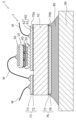
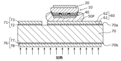
- Fig. 1 is a schematic cross-sectional view showing the overall configuration of a light-emitting device 1 according to the present embodiment.
- Fig. 1 shows a cross section perpendicular to the propagation direction of light emitted by the light-emitting device 1.
- the light-emitting device 1 includes a semiconductor laser element 10, a base 70, and a first bonding layer 30.
- the light-emitting device 1 further includes a first electrode 20.
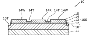
- the semiconductor laser element 10 is an edge-emitting semiconductor light-emitting element that emits laser light from the side (edge) of the element.
- the semiconductor laser element 10 includes a semiconductor laminate 10S.
- the configuration and dimensions of the semiconductor laser element 10 are not particularly limited.
- the semiconductor laser element 10 may emit, for example, infrared light, visible light, or ultraviolet light. In this embodiment, the semiconductor laser element 10 emits blue laser light.
- the length (in the resonance direction) of the semiconductor laser element 10 may be about 1.2 mm, the width may be about 150 ⁇ m, and the thickness may be about 80 ⁇ m.
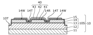
- the semiconductor laser element 10 according to this embodiment includes a substrate 11, a semiconductor laminate 10S, and an insulating film 15.
- the semiconductor laser element 10 is junction-down mounted on the base 70.
- the semiconductor laminate 10S of the semiconductor laser element 10 is bonded to the base 70 via the first bonding layer 30 or the like.
- a portion of the semiconductor laminate 10S generates heat, so bonding the surface on which the semiconductor laminate 10S is formed to the base 70 can achieve higher heat dissipation than bonding the substrate 11 to the base 70.
- the light-emitting device 1 in which the semiconductor laser element 10 is junction-down mounted as in this embodiment can enhance the effect of improving heat dissipation.
- the substrate 11 is a plate-like member that serves as the base for the semiconductor laser element 10.
- the semiconductor laminate 10S is a laminate including multiple semiconductor layers stacked on a substrate 11, and includes a pn junction.
- the semiconductor laminate 10S has a first semiconductor layer 12 including a semiconductor of a first conductivity type, an active layer 13 that generates light, and a second semiconductor layer 14 including a semiconductor of a second conductivity type different from the first conductivity type.
- the first conductivity type and the second conductivity type are n-type and p-type, respectively.
- the semiconductor laminate 10S has an opposing surface 10Sa that faces the substrate 11, a back surface 10Sb on the back side of the opposing surface 10Sa, and a side surface 10Sc that is connected to the opposing surface 10Sa and extends along the resonance direction of the semiconductor laser element 10.
- the semiconductor laminate 10S has a ridge stripe 14R, two grooves 14T, two raised portions 14W, and two laminate recesses 10T.
- the two grooves 14T are recesses formed on the back surface 10Sb of the semiconductor laminate 10S and extend parallel to the resonance direction of the laser light in the semiconductor laser element 10.
- the two grooves 14T are formed in the second semiconductor layer 14.
- the ridge stripe 14R is disposed on the back surface 10Sb behind the facing surface 10Sa of the semiconductor laminate 10S that faces the substrate 11, and is a convex portion that extends parallel to the resonance direction of the laser light in the semiconductor laser element 10.
- the ridge stripe 14R protrudes in a direction away from the substrate 11 (upward in Figure 1).
- the ridge stripe 14R is a structure for confining the current supplied to the active layer 13 to the central portion in the horizontal direction in Figure 1, and also functions as an optical waveguide.
- the longitudinal direction of the ridge stripe 14R is the resonance direction of the laser light.
- the width of the ridge stripe 14R (the horizontal dimension in FIG. 1) is 45 ⁇ m.
- the width of the ridge stripe 14R is designed according to the expected value of the operating optical output. Generally, in order to achieve a high operating optical output in the semiconductor laser element 10, the width of the ridge stripe 14R needs to be large. This is to reduce the optical density at the laser light emission end face and avoid the occurrence of a destructive phenomenon called COD (catastrophic optical damage). However, if the width of the ridge stripe 14R is increased, the current required for laser oscillation, i.e., the oscillation threshold current, increases, and the temperature of the semiconductor laser element 10 rises.
- the designer determines an appropriate width of the ridge stripe 14R taking into consideration the expected optical output, the laser characteristics of the semiconductor laser element, the thermal resistance of the entire light-emitting device 1, and the like.
- the width of the ridge stripe 14R is often designed to be about 1 ⁇ m or more and 100 ⁇ m or less.
- Each of the two raised portions 14W is a region between the groove 14T and the side surface 10Sc of the semiconductor laminate 10S, and is a convex portion that protrudes in a direction away from the substrate 11 relative to the bottom of the groove 14T.
- the groove 14T is disposed between each of the two raised portions 14W and the ridge stripe 14R.
- the two laminate recesses 10T are located between the back surface 10Sb and the side surface 10Sc of the semiconductor laminate 10S, and are recesses recessed with respect to the back surface 10Sb and the side surface 10Sc.
- the side surface 10Sc is the end surface in the lateral direction (perpendicular to the stacking direction of the semiconductor laminate 10S and the resonance direction of the laser light) of the semiconductor laminate 10S shown in FIG. 1.
- the side surface 10Sc is a surface of the surface of the semiconductor laminate 10S that is connected to the opposing surface 10Sa and extends along the resonance direction of the laser light of the semiconductor laser element 10.
- the depth of the laminate recess 10T from the back surface 10Sb toward the substrate 11 is deeper than the depth from the back surface 10Sb to the pn junction, and reaches halfway through the first semiconductor layer 12.
- the laminate recess 10T may be part of an element isolation groove formed when the semiconductor laser element 10 is singulated.
- the laminate recess 10T is also covered with an insulating film 15. In other words, the insulating film 15 covers the first semiconductor layer 12 in the stack recess 10T.
- the insulating film 15 covers a part of the semiconductor laminate 10S.
- the insulating film 15 is disposed on the back surface 10Sb of the semiconductor laminate 10S.
- the insulating film 15 covers the entire surface of the ridge stripe 14R except for the top surface of the ridge stripe 14R.
- the insulating film 15 continuously covers the area from one laminate recess 10T to one side surface of the ridge stripe 14R, and also continuously covers the area from the other laminate recess 10T to the other side surface of the ridge stripe 14R.
- the insulating film 15 is disposed between the semiconductor laminate 10S and the adhesion layer 42.
- the material of the insulating film 15 is a silicon oxide film having a thickness of 300 nm.
- the first electrode 20 is a conductive member disposed on the substrate 11.
- the first electrode 20 is disposed on the principal surface of the substrate 11, the principal surface being the back side of the principal surface on which the semiconductor laminate 10S is laminated.
- the first electrode 20 has an ohmic electrode layer 21 and a pad electrode layer 22.
- the ohmic electrode layer 21 is an electrode that contacts the substrate 11. An electrical ohmic contact is formed at the interface between the ohmic electrode layer 21 and the substrate 11.
- the ohmic electrode layer 21 may have a function of increasing the adhesion between the substrate 11 and the pad electrode layer 22.
- the ohmic electrode layer 21 may be, for example, a single layer or a multilayer film made of at least one of Ti, Al, Cr, Ag, Ni, Pd, and Pt.
- the pad electrode layer 22 is a conductive layer for supplying power to the semiconductor laser element 10.
- a wire (described later) is connected to the pad electrode layer 22.
- the pad electrode layer 22 may be, for example, a single layer film made of Au.
- the pad electrode layer 22 is an Au film having a thickness of 0.3 ⁇ m or less.
- the first bonding layer 30 is a conductive layer that bonds the base 70 and the semiconductor laser element 10.
- the first bonding layer 30 has a second electrode 40, a metal film 50, and a base electrode 60, which are arranged in this order from the semiconductor laser element 10 toward the base 70.
- the second electrode 40 is a conductive member disposed on the semiconductor laminate 10S.
- the second electrode 40 is disposed on the back surface 10Sb of the semiconductor laminate 10S.
- the second electrode 40 has an element junction layer 43.
- the second electrode 40 further has an ohmic electrode layer 41 and an adhesion layer 42.
- the ohmic electrode layer 41 is an electrode that contacts the semiconductor laser element 10.
- the ohmic electrode layer 41 is in ohmic contact with the second semiconductor layer 14 of the semiconductor laminate 10S.
- the ohmic electrode layer 41 is disposed on the upper surface of the ridge stripe 14R (i.e., the surface of the ridge stripe 14R that is located farthest from the substrate 11).
- the ohmic electrode layer 41 may be, for example, a single layer or a multilayer film made of at least one of Pd, Ni, Pt, Au, Ag, W, Ti, and Al. Metal oxides such as ITO and ZnO may also form ohmic contact. However, these materials have low thermal conductivity and are disadvantageous materials in terms of heat dissipation.
- the ohmic electrode layer 41 is a Pd film with a thickness of 0.1 ⁇ m or less.
- the adhesion layer 42 is a conductive layer disposed between the ohmic electrode layer 41 and the element bonding layer 43.
- the adhesion layer 42 may have a function of increasing the adhesion between the semiconductor laser element 10 and the element bonding layer 43.
- the adhesion layer 42 may cover the ohmic electrode layer 41.
- the adhesion layer 42 may be, for example, a single layer film made of Ti, Cr, or Ni. These materials that have the function of increasing adhesion have low thermal conductivity and are disadvantageous in terms of heat dissipation. Therefore, the thickness may be as thin as possible.
- the adhesion layer 42 is a Ti film having a thickness of 0.1 ⁇ m or less.
- the element bonding layer 43 is a metal layer disposed between the semiconductor laser element 10 and the metal film 50.
- the element bonding layer 43 is a conductive layer bonded to a conductor for supplying power to the semiconductor laser element 10.
- the element bonding layer 43 also plays a role in efficiently transferring heat generated in the semiconductor laser element 10 to the base 70. Therefore, the element bonding layer 43 is composed of a single metal element. In a layer composed of a single metal element, alloy scattering of electrons and phonons does not occur, so that the electrical resistance and thermal resistance of the element bonding layer 43 can be reduced.
- the element bonding layer 43 may be selected from Au, Ag, Cu, or Al. All of these metals have a thermal conductivity of 200 W ⁇ m ⁇ 1 ⁇ K ⁇ 1 or more. These metals are characterized by having a particularly high thermal conductivity among metal materials.
- a part or all of the element bonding layer 43 contacts the metal film 50, which is a sintered body, to form a continuum.
- a part or all of the element bonding layer 43 may be composed of the same metal element as the metal film 50. This can increase the bonding strength between the element bonding layer 43 and the metal film 50.
- a sintered body of Ag forms a continuum with metals other than Ag, so the element bonding layer 43 does not necessarily have to be the same metal as the metal film 50.
- the first bonding layer 30 has a single element bonding layer 43, but may have multiple element bonding layers.
- the first bonding layer 30 may have an element bonding layer made of Cu in addition to the element bonding layer 43 made of Au.
- the multiple element bonding layers do not have to be adjacent to each other.
- other layers such as an adhesive layer, may be inserted between the two element bonding layers.
- layers made of metal elements other than the four types of Au, Ag, Cu, and Al have low thermal conductivity and are a factor that inhibits heat dissipation. Therefore, layers made of metal elements other than the four types of Au, Ag, Cu, and Al may be formed as thin as possible.
- the metal film 50 is disposed between the element bonding layer 43 and the base 70, and is a conductive film made of a single metal element.
- the metal film 50 is in contact with the element bonding layer 43.
- the metal film 50 may be a sintered body of metal fine particles formed by, for example, heating a paste in which metal fine particles are dispersed in a solvent (organic solvent) to remove the solvent and sinter the metal fine particles.
- the metal fine particles are made of, for example, Au, Ag, Cu, or Al metal.
- the average particle size of the metal fine particles measured by a scanning electron microscope is 1 ⁇ m or less.
- the average particle size is a value obtained by an intercept method in a cross-sectional image by a scanning electron microscope.
- the metal fine particles are melted by heating at a relatively low temperature of about 250 ° C., and the metal fine particles are bonded to each other (in other words, sintered).
- the paste contains metal fine particles and a solvent, but may also contain a surfactant to increase the dispersibility of the metal fine particles.
- the solvent used in the paste is, for example, an organic solvent such as ester alcohol (2,2,4-trimethyl-3-hydroxypentaisobutyrate: C 12 H 24 O 3 ), terpineol, pine oil, butyl carbitol acetate, butyl carbitol, carbitol, etc.
- the surfactant is, for example, an alkylamine (CH 3 (CH 2 ) n NH 2 ), an alkylamine carboxylate, a carboxylic acid amide, an esteramine, an organic titanium compound, sodium sulfocarboxylate, etc.
- the boiling point of the solvent may be 250°C or less, or may be 150°C or more and 230°C or less. By having the boiling point of the solvent be in the range of 150°C or more and 230°C or less, it is possible to prevent the solvent from being trapped between the sintered metal microparticles when the solvent is removed by heating.
- the metal film 50 which is a sintered body formed in this way, may become a porous film having voids.
- the porosity in terms of area ratio of the metal film 50 is, for example, less than 30%.
- the average cross-sectional area of each void is 1 ⁇ m 2 or less. This makes it possible to suppress the decrease in thermal conductivity due to voids in the metal film 50. Therefore, the heat dissipation of the semiconductor laser element 10 can be improved compared to when a solder made of AuSn is used as the metal film 50.
- the porosity in terms of area ratio in the cross section of the metal film 50 can be obtained, for example, as follows.
- the void portion is observed to have low brightness because there are few reflected electrons. Therefore, in the electron microscope photograph, a region with a brightness below a certain value can be determined as a void. Specifically, a histogram of the brightness of pixels in the measurement area can be obtained, and the ratio of the portion below a certain value can be determined as the porosity.
- the porosity of the metal film 50 depends on the pressure applied to the metal film 50 during sintering.
- the highly filled portion 50a of the metal film 50 sandwiched between the semiconductor laser element 10 and the base 70 is compressed vertically between the semiconductor laser element 10 and the base 70 during the sintering process by heating. Therefore, the metal particles in the highly filled portion 50a press against each other and are crushed. As a result, the gaps between the metal particles are filled, and the highly filled portion 50a with a low porosity is easily formed.
- the low-filling portion 50b of the metal film located outside the high-filling portion 50a is not subjected to direct pressure from the semiconductor laser element 10 and the substrate 70. Therefore, the metal particles in the low-filling portion 50b form a sintered body without pressing against each other. As a result, the gaps between the metal particles are preserved, and it is easy to form the low-filling portion 50b with a higher porosity than the high-filling portion 50a.
- the voids in the metal film 50 function to locally block the heat dissipation path. Therefore, in order to improve heat dissipation, the porosity of the metal film 50 may be low.
- the high filling portion 50a of the metal film 50 constitutes the main part of the heat dissipation path. Therefore, in this high filling portion 50a, a sintering process may be performed by applying pressure from above and below so that the void ratio is as low as possible.
- the void ratio of the high filling portion 50a is lower than that of the low filling portion 50b.
- the average cross-sectional area of the individual voids in the low filling portion 50b is greater than the average cross-sectional area of the individual voids in the high filling portion 50a.
- the metal film 50 is made of a single metal element. As a result, alloy scattering of electrons and phonons does not occur in the metal film 50, so that the electrical resistance and thermal resistance of the metal film 50 can be reduced.
- the metal film 50 is made of Au, Ag, Cu, or Al. All of these metals have a thermal conductivity of 200 W ⁇ m ⁇ 1 ⁇ K ⁇ 1 or more. In other words, these metals are characterized by having particularly high thermal conductivity among metal materials.
- the metal film 50 is made of Au.
- the thickness of the metal film 50 is, for example, 3 ⁇ m or more.
- the melting point of the Au metal film 50 formed as a sintered body in this way has a value close to the melting point of 1064° C.
- the metal film 50 does not melt even if it is heated to about 300° C. to melt the solder. Therefore, in the light-emitting device 1, changes in the relative position and attitude of the semiconductor laser element 10 with respect to the base 70 when the light-emitting device 1 is mounted on the mounting base can be suppressed.
- the thickness of the metal film 50 may be 10 ⁇ m or less. This reduces the thermal resistance of the metal film 50, thereby improving the heat dissipation properties of the light-emitting device 1.
- the metal film 50, the pad electrode layer 22, and the substrate bonding layer 62 described below may be made of the same metal element. This can increase the bonding strength between the metal film 50 and the pad electrode layer 22 and substrate bonding layer 62.
- the metal film 50 has an extension 50e that extends outward from the side surface of the semiconductor laser element 10 (i.e., the side surface 10Sc of the semiconductor laminate 10S) in the horizontal direction in a cross-sectional view perpendicular to the resonance direction (i.e., in the left-right direction in FIG. 1).
- the metal film 50 extends outward from the side surface of the semiconductor laser element 10 in the horizontal direction in a cross-sectional view perpendicular to the resonance direction (i.e., in the left-right direction in FIG. 1).
- the surface of the extension 50e has a convex shape. In other words, the surface of the extension 50e protrudes outward. This increases the number of heat dissipation paths that diffuse outward from the end of the surface of the semiconductor laser element 10 that faces the base 70, thereby improving the heat dissipation properties of the semiconductor laser element 10.
- the maximum height h1 of the extension 50e from the base 70 may be greater than the minimum distance d1 from the base 70 to the element bonding layer 43.
- the maximum thickness of the extension 50e of the metal film 50 may be greater than the minimum thickness of the portion of the metal film 50 that contacts the second electrode 40 and the base electrode 60. This allows the extension 50e to block a portion of the leaked light (spontaneous emission light) from the side surface 10Sc of the semiconductor laminate 10S.
- the metal film 50 contacts the insulating film 15 on the laminate recess 10T, but it does not have to be in contact. This makes it possible to prevent the metal film 50 from contacting the pn junction exposed in the laminate recess 10T.
- the metal film 50 may be disposed in the groove 14T of the semiconductor laminate 10S. In other words, a portion of the metal film 50 may be disposed in a position facing a side surface of the ridge stripe 14R that extends along the resonance direction.
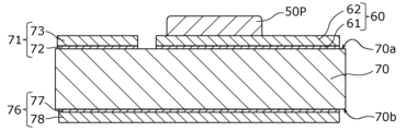
- the substrate electrode 60 is a conductive member disposed between the metal film 50 and the substrate 70.
- the substrate electrode 60 is disposed on the first main surface 70a of the substrate 70.
- the substrate electrode 60 has a substrate bonding layer 62.
- the substrate electrode 60 further has a substrate adhesion layer 61.
- the substrate adhesion layer 61 is a conductive layer disposed between the substrate 70 and the substrate bonding layer 62. In this embodiment, the substrate adhesion layer 61 contacts the first main surface 70a of the substrate 70.
- the substrate adhesion layer 61 may have a function of increasing adhesion between the first main surface 70a of the substrate 70 and the substrate bonding layer 62.
- the substrate adhesion layer 61 may be, for example, a single layer film made of Ti, Cr, or Ni. These materials that have the function of increasing adhesion have low thermal conductivity and are disadvantageous in terms of heat dissipation. Therefore, the thickness may be as thin as possible.
- the substrate adhesion layer 61 is a Ti film having a thickness of 0.1 ⁇ m or less.
- the substrate bonding layer 62 is disposed between the metal film 50 and the substrate 70, and is a conductive layer made of a single metal element. As described above in the description of the element bonding layer 43, the substrate bonding layer 62 may be selected from Au, Ag, Cu, or Al. All of these metals have a thermal conductivity of 200 W ⁇ m ⁇ 1 ⁇ K ⁇ 1 or more. These metals are characterized by having particularly high thermal conductivity among metallic materials.
- the substrate bonding layer 62 contacts the metal film 50, which is a sintered body, to form a continuum. For this reason, it may be composed of the same metal element as the metal film 50. This makes it possible to increase the bonding strength between the substrate bonding layer 62 and the metal film 50.
- the substrate bonding layer 62 does not necessarily have to be made of the same metal as the metal film 50.
- the first bonding layer 30 has a single substrate bonding layer 62, but may have multiple substrate bonding layers.
- the first bonding layer 30 may have a substrate bonding layer made of Cu in addition to the substrate bonding layer 62 made of Au.
- the multiple substrate bonding layers do not have to be adjacent to each other.
- other layers such as an adhesive layer, may be inserted between the two substrate bonding layers.
- metal layers other than the four types of Au, Ag, Cu, and Al have low thermal conductivity, which is a factor that inhibits heat dissipation. Therefore, metal layers other than the four types of Au, Ag, Cu, and Al may be formed as thin as possible.
- the substrate bonding layer 62 is an Au film with a thickness of 0.3 ⁇ m or less.
- the total thickness of the element bonding layer 43, metal film 50, and substrate bonding layer 62 included in the first bonding layer 30 is 80% or more of the thickness of the first bonding layer 30. In this way, by increasing the proportion of the thickness of the portion of the first bonding layer 30 that is made of a single metal element, the electrical resistance of the first bonding layer 30 can be reduced. Therefore, the ohmic loss and heat generation in the light-emitting device 1 can be reduced.
- the base 70 is a base on which the semiconductor laser element 10 is bonded.
- the base 70 has a first main surface 70a on which the semiconductor laser element 10 is bonded, and a second main surface 70b located on the back side of the first main surface 70a.
- the base 70 has a rectangular parallelepiped shape.
- the light-emitting device 1 according to this embodiment is often used in a state in which it is electrically connected to one or more other light-emitting devices 1.
- the multiple light-emitting devices 1 are mounted on a metal heat sink and electrically connected to each other in series or in parallel.
- the base 70 of each of the multiple light-emitting devices 1 may be made of an electrically insulating material.
- the semiconductor laser element 10 used in this embodiment is a GaN-based semiconductor laser element mainly made of GaN.
- the thermal expansion coefficient of GaN is about 3 ⁇ 10 ⁇ 6 K ⁇ 1 (at room temperature, in the in-plane direction of the c-plane).
- the thermal expansion coefficients of Cu and Al, which are often used for heat sinks are 17 ⁇ 10 ⁇ 6 K ⁇ 1 and 23 ⁇ 10 ⁇ 6 K ⁇ 1 , respectively, which are much larger than that of GaN.
- the thermal strain can be alleviated by connecting the semiconductor laser element 10 to the heat sink via a base 70 made of SiC ceramic, AlN ceramic, or the like. This is because the thermal expansion coefficients of these materials are about 4 ⁇ 10 ⁇ 6 K ⁇ 1 , which is close to that of GaN.
- a base 70 with a small thermal expansion coefficient can be constructed.
- W tungsten
- CuW copper-tungsten alloy
- Mo mobdenum
- CuMo copper-molybdenum alloy
- the semiconductor laser element When using a laser array element called a laser bar as the semiconductor laser element, the semiconductor laser element may be directly bonded to a Cu heat sink. However, thermal distortion still remains an issue.
- synthetic diamond having a thermal conductivity of 1000 W ⁇ m ⁇ 1 ⁇ K ⁇ 1 or more can also be used as the substrate 70.
- single crystal SiC can be used if the electrical resistance is sufficiently high. These materials also do not have a high thermal expansion coefficient like metals, and are therefore useful as materials for the substrate 70.
- the substrate 70 is made of SiC ceramic.
- the operating voltage is higher and the WPE (Wall-Plug Efficiency) is lower than, for example, a GaAs-based semiconductor laser element.
- the WPE Wide-Plug Efficiency
- Fig. 2 is a schematic cross-sectional view showing the overall configuration of a light emitting module 5 according to the present embodiment.
- Fig. 2 shows a cross section perpendicular to the propagation direction of light emitted by the light emitting module 5.
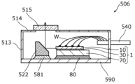
- the light-emitting module 5 of this embodiment includes a light-emitting device 1, a heat sink 90, and a second bonding layer 80.
- the light-emitting device 1 shown in FIG. 2 includes the components of the light-emitting device 1 shown in FIG. 1, as well as a relay electrode 71 and a back metal layer 76.
- the relay electrode 71 is an electrode disposed on the substrate 70.
- the relay electrode 71 is electrically insulated from the substrate electrode 60.
- the relay electrode 71 is disposed on the first main surface 70a of the substrate 70.
- the relay electrode 71 may be used to relay a power supply path for supplying power to the first electrode 20.
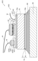
- the relay electrode 71 may be bonded with a wire W connected to a power source (not shown) and a wire W connected to the first electrode 20.
- a wire W connected to a power source is connected to the substrate electrode 60.
- These wires W are an example of a power supply conductor for supplying power to the semiconductor laser element 10.
- the relay electrode 71 has a substrate adhesion layer 72 and a pad electrode layer 73.
- the relay electrode 71 may have the same layer structure as the substrate electrode 60.
- the relay electrode 71 may be formed simultaneously with the substrate electrode 60 in the same process.
- the light-emitting device 1 does not need to include the relay electrode 71. In this case, for example, a wire W may be bonded directly from the power source to the first electrode 20.
- the back metal layer 76 is a metal layer disposed on the second main surface 70b of the base 70.
- the back metal layer 76 may have the function of increasing the adhesion between the base 70 and the heat sink 90.
- the back metal layer 76 has a back adhesion layer 77 and a back bonding layer 78.
- the back adhesion layer 77 is a metal layer disposed between the substrate 70 and the back adhesion layer 78. In this embodiment, the back adhesion layer 77 contacts the second main surface 70b of the substrate 70. The back adhesion layer 77 may have a function of increasing the adhesion between the second main surface 70b of the substrate 70 and the back adhesion layer 78.
- the back adhesion layer 77 may be, for example, a single layer film made of Ti, Cr, or Ni. In this embodiment, the back adhesion layer 77 is a Ti film having a thickness of 0.1 ⁇ m or less.
- the back surface bonding layer 78 is a conductive layer disposed between the substrate 70 and the second bonding layer 80.
- the back surface bonding layer 78 is a layer made of a single metal element.
- the back surface bonding layer 78 may be, for example, a single layer film made of Au.
- the back surface bonding layer 78 is an Au film having a thickness of 0.3 ⁇ m or less.
- the heat sink 90 is a member for dissipating heat generated by the light emitting device 1.
- the heat sink 90 also functions as a mounting base on which the light emitting device 1 is mounted.
- the base 70 of the light emitting device 1 is joined to the heat sink 90.
- the heat sink 90 has, for example, a plate shape and is made of a material with high thermal conductivity such as Cu or Al.
- the heat sink 90 may have a surface treatment layer made of, for example, Ni, Cr, Au, etc., on the surface on the second bonding layer 80 side, which has good adhesion to the second bonding layer 80.
- the second bonding layer 80 is a bonding member that bonds the base 70 and the heat sink 90.
- the second bonding layer 80 is disposed between the heat sink 90 and the back metal layer 76.
- the heat sink 90 is bonded to the second main surface 70b of the base 70 via the back metal layer 76.
- the melting point of the second bonding layer 80 must be lower than that of the first bonding layer 30.
- a sintered body with a high melting point is used for the metal film 50 of the first bonding layer 30. Therefore, a material with a relatively high melting point can be selected for the second bonding layer 80.
- the second bonding layer 80 is made of, for example, AuSn, SnAgCu, etc., and can firmly bond the base 70 and the heat sink 90. To use these materials, heating to nearly 300°C is required, but the heat treatment can be performed without melting the first bonding layer 30.
- the second bonding layer 80 is an AuSn film with a thickness of 5 ⁇ m or less.
- Fig. 3 to Fig. 11 and Fig. 13 are schematic cross-sectional views showing each step of the method for manufacturing the light emitting device 1 according to the present embodiment.
- Fig. 12 is a schematic perspective view showing a ninth step of the method for manufacturing the light emitting device 1 according to the present embodiment.
- a semiconductor laminate 10S is formed above a substrate 11.
- the semiconductor laminate 10S can be laminated, for example, using a MOCVD (Metal Organic Chemical Vapor Deposition) method.
- MOCVD Metal Organic Chemical Vapor Deposition
- the stack recess 10T, the protuberance 14W, the groove 14T, and the ridge stripe 14R are formed in the semiconductor stack 10S.
- the stack recess 10T and the groove 14T are formed in the semiconductor stack 10S using photolithography, etching, and the like.
- the stack recess 10T is formed on both side surfaces of the semiconductor stack 10S.
- Two grooves 14T are also formed.
- the protuberance 14W is formed between the stack recess 10T and the groove 14T
- the ridge stripe 14R is formed between the two grooves 14T.
- the stack recess 10T may be a part of an element isolation groove formed when the semiconductor laser element 10 is divided into individual pieces.
- the depth of the groove is deeper than the depth from the back surface 10Sb of the semiconductor stack 10S to the pn junction, so that the pn junction is less likely to be altered by processing when the elements are isolated by dicing or the like.
- the insulating film 15 is formed.
- the insulating film 15 is disposed on the entire upper surface of the semiconductor laminate 10S shown in FIG. 5, except for the upper surface of the ridge stripe 14R, by using a CVD (Chemical Vapor Deposition) method and etching.
- CVD Chemical Vapor Deposition
- an element bonding layer 43 is formed on the semiconductor laser element 10 (element bonding layer forming process).
- a second electrode 40 including the element bonding layer 43 is formed above the semiconductor laminate 10S.
- each layer of the second electrode 40 is formed by photolithography technology, deposition method, etc.
- a first electrode 20 is formed on the rear surface of the substrate 11 (i.e., of the two main surfaces of the substrate 11, the main surface on the rear side of the main surface on which the semiconductor laminate 10S is disposed).
- each layer of the first electrode 20 is formed by photolithography technology, deposition method, etc.
- a substrate bonding layer 62 is formed on the substrate 70 (substrate bonding layer formation process).
- a substrate electrode 60 including the substrate bonding layer 62 and a relay electrode 71 are formed on the first main surface 70a of the substrate 70.
- the substrate electrode 60 and the relay electrode 71 are formed by photolithography technology, vapor deposition, or the like.
- the substrate electrode 60 and the relay electrode 71 may be formed simultaneously in the same process.
- a back metal layer 76 is formed on the second main surface 70b of the substrate 70.
- the back metal layer 76 is formed by photolithography, deposition, or the like.
- a paste 50P in which metal particles are dispersed in a solvent is applied onto the base bonding layer 62 (application process).
- the paste 50P is patterned as it is applied. This makes it possible to reduce the amount of paste 50P used and the time required to manufacture the light-emitting device 1, compared to, for example, applying the paste 50P to the entire surface of the first main surface 70a and then patterning it.
- the embodiment of the application process is not particularly limited. In the application process, for example, a method using a transfer pin, silk screen printing, a dispenser method, inkjet printing, etc. can be used.
- the viscosity of the paste 50P may be, for example, 10 Pa ⁇ s or more. This allows the amount of solvent contained in the paste 50P to be reduced, thereby suppressing deformation caused by a reduction in volume when the paste 50P is heated. In addition, the heating time required to sinter the paste 50P can be reduced.
- the element bonding layer 43 formed on the semiconductor laser element 10 is placed on the paste 50P (placement process).
- the semiconductor laser element 10 is placed so that the light emission surface 10E protrudes from the edge 70E of the first main surface of the base 70. This makes it possible to prevent the base 70 from blocking the emitted light of the semiconductor laser element 10.
- the entire surface of the laminate recess 10T is covered with an insulating film 15.
- the insulating film 15 covers the first semiconductor layer 12 in the laminate recess 10T. This makes it possible to prevent a short circuit from occurring between the pn layers of the semiconductor laminate even if the paste 50P containing metal particles that protrudes toward the side of the semiconductor laminate 10S during the placement process extends into the laminate recess 10T.
- the paste 50P is heated and sintered to form the metal film 50 (sintering process).
- the base 70 and the like are heated in a bake furnace or the like at 200°C for about 30 minutes, and then cooled.
- This forms the metal film 50 which is a sintered body of metal particles, and the element bonding layer 43 and the base bonding layer 62 can be bonded by the metal film 50.
- the base 70 and the semiconductor laser element 10 can be bonded.
- bonding can be performed at a relatively low temperature as described above. Therefore, damage to the semiconductor laser element 10 caused by heating can be reduced.
- the manufacturing method of the light-emitting device 1 may include a removal step between the application step and the placement step, in which the paste 50P is heated to remove the solvent. This makes it possible to stabilize the amount of solvent contained in the paste 50P in the placement step, thereby suppressing variation in the characteristics of the light-emitting device 1 due to factors such as the shape of the paste 50P, which are influenced by fluctuations in the waiting time before the placement step.
- a light-emitting device 1 as shown in Figure 2 can be formed.
- Figures 14 to 16 are schematic cross-sectional views showing each step of the method for manufacturing a light-emitting module 5 according to this embodiment.
- the second bonding layer 80 is placed on the heat sink 90 (second bonding layer placement process).
- the base 70 of the light-emitting device 1 is placed on the second bonding layer 80 (base placement process). Specifically, the light-emitting device 1 is placed on the second bonding layer 80 so that the second main surface 70b of the base 70 faces the second bonding layer 80. Here, the base 70 may be pressed against the heat sink 90. This can increase the adhesion between the back metal layer 76, which is placed on the second main surface 70b of the base 70, and the second bonding layer 80.
- the second bonding layer 80 is heated to melt the second bonding layer 80.
- This bonds the base 70 to the heat sink 90 (bonding process).
- the heat sink 90 is heated at 300°C in a baking furnace or the like for about 1 minute, and then cooled. This allows the heat sink 90 and the back surface metal layer 76 to be bonded by the second bonding layer 80. In other words, the base 70 and the heat sink 90 can be bonded.
- the above steps allow the light emitting module 5 shown in FIG. 2 to be manufactured.
- a metal film 50 of a sintered body having a high melting point is used for the first bonding layer 30.
- the light emitting device 1 can be firmly bonded to the heat sink 90 by using AuSn solder, which has a relatively high melting point.
- the first bonding layer 30 that connects the semiconductor laser element 10 to the base 70 does not remelt. Therefore, changes in the relative position and posture of the semiconductor laser element 10 with respect to the base 70 can be suppressed.
- the manufacturing process of the light emitting module 5 can be completed while suppressing changes in the initial heat dissipation. In other words, even after the mounting process on the heat sink 90, changes in the basic characteristics of the semiconductor laser element 10 can be suppressed.
- Heat generated in the semiconductor laser element 10 is locally concentrated in a strip-shaped area corresponding to the position of the ridge stripe 14R. This is because the current required to drive the laser is concentrated in the area of the ridge stripe 14R. In addition, since the guided light is also confined to the area corresponding to this portion, heat generated by scattering and absorption is also concentrated in this area. This is significantly different from general electronic devices and light-emitting diodes, in which heat sources are widely distributed within the surface of the element.
- the thermal resistance of the portion adjacent to the semiconductor laser element 10, that is, the first bonding layer 30 in this embodiment is extremely important. How quickly the heat dissipation path from the band-shaped heat source can be expanded laterally greatly affects the thermal resistance of the entire heat dissipation path of the light-emitting module 5. If the heat dissipation path cannot be expanded laterally quickly, only a part of the area of the base 70 functions as a heat dissipation path, and the thermal resistance of the entire system cannot be reduced.
- This problem is more susceptible to the narrower the width of the ridge stripe 14R, and is significant when the width of the ridge stripe 14R is 100 ⁇ m or less.
- a metal material is used as the base 70, and it is important to reduce the thermal resistance of the first bonding layer 30 including the base bonding layer 62 formed on the surface of the base 70.
- a single element layer of Au which has high thermal conductivity, is used for the element bonding layer 43, the metal film 50 of the sintered body, and the base bonding layer 62, so that the total thickness of the layers of the first bonding layer 30 made of a single metal element of any of Au, Ag, Cu, and Al is 80% or more of the entire thickness of the first bonding layer 30.
- the heating temperature in the sintering process may be lower than the heating temperature in the bonding process. This reduces damage to the semiconductor laser element 10 caused by heating in the sintering process.
- the light emitting module according to the present embodiment differs from the light emitting module 5 according to the first embodiment mainly in that the light emitting module combines and outputs a plurality of laser beams from a plurality of light emitting devices 1, and that the light emitting devices 1 are hermetically sealed.
- the volume of the member corresponding to the heat sink (the multi-stage base 190 and the module substrate 112 described later) is inevitably large. When the volume of the member is large, the heat capacity of the member is also large, so that rapid heating and rapid cooling are difficult.
- Fig. 17 is a schematic perspective view showing the overall configuration of a light emitting module 106 according to the present embodiment.
- the light emitting module 106 includes a module substrate 112, a frame 113, a multi-stage base 190, six light emitting devices 1, six FAST axis collimator lenses 120, six SLOW axis collimator lenses 121, six reflecting mirrors 122, a focusing lens 123, an optical fiber 124, and two current introduction terminals 140.
- the module substrate 112 is a plate-like member that serves as the base for the light-emitting module 106.
- the module substrate 112 is made of, for example, Cu or Al.
- the module substrate 112 is used by being fixed to, for example, a temperature control stage using a Peltier element, a cooling stage equipped with a water-cooling mechanism, or the like (not shown).
- the frame 113 is an annular side wall that is erected on the module substrate 112. In this embodiment, the frame 113 has a rectangular annular shape. In FIG. 17, a portion of the frame 113 is cut out to show the internal structure of the frame 113 of the light-emitting module 106.
- the frame 113 is made of an Fe-based material, such as Fe, an FeNi alloy, or stainless steel.
- the light-emitting module 106 is disposed on the frame body 113 and has a plate-shaped lid that covers the opening of the frame body 113 (see the lid 114 shown in FIG. 22 described later).
- the lid is made of an Fe-based material such as Fe, FeNi alloy, or stainless steel.
- the module substrate 112, frame body 113, and lid form a housing.
- the light-emitting device 1 and the like are disposed inside the housing.
- the current introduction terminals 140 are terminals for introducing current from the outside of the frame body 113 to the inside of the frame body 113.
- One end of each of the two current introduction terminals 140 is disposed on the outside of the frame body 113, and the other end is disposed on the inside of the frame body 113.
- the current introduction terminals 140 are disposed on the frame body 113 and penetrate the frame body 113. If the frame body 113 is formed of a conductive material, an insulating member is disposed between the current introduction terminals 140 and the frame body 113.
- the multi-stage base 190 and the module substrate 112 correspond to the heat sink in the first embodiment.
- the multi-stage base 190 is a member having a plurality of laser mounting surfaces 191 and a plurality of optical element mounting surfaces 192.
- the multi-stage base 190 has six flat rectangular laser mounting surfaces 191 and six flat rectangular optical element mounting surfaces 192.
- the multi-stage base 190 has six stair-shaped steps.
- the six laser mounting surfaces 191 correspond to the step surfaces (surfaces parallel to the main surface of the module substrate 112) of the plurality of stair-shaped steps.
- the six laser mounting surfaces 191 are at different heights from the module substrate 112.
- the six optical element mounting surfaces 192 correspond to the step surfaces of the plurality of stair-shaped steps.
- the six laser mounting surfaces 191 are at different heights from the module substrate 112. Each of the six laser mounting surfaces 191 is adjacent to each of the six optical element mounting surfaces 192. In this embodiment, the six laser mounting surfaces 191 and the six optical element mounting surfaces 192 are at different heights from the module substrate 112, but they may be the same height.
- the multi-stage base 190 is made of, for example, Cu, Al, or the like. In this embodiment, the six laser mounting surfaces 191 and the six optical element mounting surfaces 192 of the multi-stage base 190 are plated with Au. This makes it easier to join the laser mounting surfaces 191 and the optical element mounting surfaces 192 with solder such as AuSn.
- Each of the six light-emitting devices 1 has the same configuration as the light-emitting device 1 according to the first embodiment.
- the six light-emitting devices 1 are respectively arranged on six laser mounting surfaces 191 of the multi-stage base 190.
- Each of the six light-emitting devices 1 emits laser light above the adjacent optical element mounting surface 192, parallel to the optical element mounting surface 192.
- the optical axes of the six laser lights emitted from the six light-emitting devices 1 are parallel to each other.
- Each of the six light-emitting devices 1 is supplied with power from a current introduction terminal 140.
- the six light-emitting devices 1 are connected in series between two current introduction terminals 140. This makes it possible to reduce the output current of the power source for supplying power.
- the six light-emitting devices 1 may also be connected in parallel.
- a wire (not shown) can be used as a power supply conductor connecting between the current introduction terminal 140 and the light emitting device 1, and between two light emitting devices 1, for example.
- the wire is bonded to the current introduction terminal 140 and the light emitting device 1 inside the frame body 113.
- Each of the six FAST axis collimator lenses 120 is a lens that collimates the laser light emitted from the light-emitting device 1 in the FAST axis direction (in this embodiment, the direction perpendicular to the laser installation surface 191).
- the six FAST axis collimator lenses 120 are disposed near the light emission surfaces of the six light-emitting devices 1, respectively.
- Each of the six FAST axis collimator lenses 120 may be disposed on the base 70 of the light-emitting device 1, or on the laser installation surface 191.
- Each of the six SLOW-axis collimator lenses 121 is a lens that collimates the laser light emitted from the FAST-axis collimator lens 120 in the SLOW-axis direction (a direction perpendicular to the FAST-axis direction and the propagation direction of the laser light).
- the six SLOW-axis collimator lenses 121 are arranged on the six optical element mounting surfaces 192, respectively.
- Each of the six SLOW-axis collimator lenses 121 collimates the laser light (laser light emitted from the FAST-axis collimator lens 120) from the light-emitting device 1 arranged on the laser mounting surface 191 adjacent to the optical element mounting surface 192 on which the lens itself is arranged.
- Each of the six reflecting mirrors 122 has the role of changing the direction of travel of the laser light emitted from the SLOW axis collimator lens 121.
- the six reflecting mirrors 122 are arranged on the six optical element mounting surfaces 192, respectively.
- each of the six reflecting mirrors 122 bends the direction of travel of the laser light by 90 degrees.
- the laser light emitted from each of the six reflecting mirrors 122 enters the focusing lens 123.
- the optical axes of the six laser lights emitted from the six reflecting mirrors 122 are parallel to each other.
- the six reflecting mirrors 122 are disposed on six optical element mounting surfaces 192 that are respectively at different heights from the module substrate 112, and the heights from the module substrate 112 of the optical axes of the six laser beams incident on the six reflecting mirrors 122 are also different from each other. Therefore, the heights from the module substrate 112 of the optical axes of the six laser beams output from the six reflecting mirrors 122 are different from each other. Therefore, the six laser beams output from the six reflecting mirrors 122 can enter the focusing lens 123 without interfering with the six reflecting mirrors 122.
- the focusing lens 123 is a lens that focuses the six laser beams reflected by the six reflecting mirrors 122.
- the six laser beams are focused by the focusing lens 123 so that most of the six laser beams are incident on the end face of the optical fiber 124 and can propagate through the optical fiber 124. In other words, they are spatially combined.
- an aspheric lens can be used as the focusing lens 123.
- the optical fiber 124 is a member that guides the laser light from the inside to the outside of the frame 113. As described above, the six laser lights emitted from the focusing lens 123 are incident on the end face of the optical fiber 124 that is located on the inside of the frame 113.
- a light-emitting module 106 having such a configuration can realize a high-power laser light source. Note that, in the example shown in FIG. 17, the number of light-emitting devices 1, etc. is six, but the number of light-emitting devices 1, etc. is not limited to six, and may be two or more.
- FIG. 18 to Fig. 22 are schematic perspective views showing each step of the method for manufacturing the light emitting module 106 according to the present embodiment.
- a multi-stage base 190 and a frame 113 on which a current introduction terminal 140 is arranged are placed on a module substrate 112.
- a second bonding layer 80 is also placed on each of the six laser mounting surfaces 191 of the multi-stage base 190.
- Each of the six light-emitting devices 1 is placed on the second bonding layer 80 placed on each of the six laser mounting surfaces 191.
- the second bonding layer 80 is melted by heating at 300° C. or higher and 350° C. or lower for about 1 minute to 60 minutes.
- the heating temperature and heating time are set to appropriate values depending on the volume of the module substrate 112 and the multi-stage base 190, which correspond to the heat sink. As mentioned above, if the volume of the heat sink increases, the heat capacity also increases, making rapid heating and cooling difficult. Therefore, the heating conditions must be higher in temperature and longer in time.
- each light-emitting device 1 can be bonded to each laser mounting surface 191 by the second bonding layer 80.
- a solder made of AuSn is used as the second bonding layer 80.
- the six light-emitting devices 1 are connected in series by wire bonding, and the light-emitting devices 1 at both ends of the series connection are connected to the two current introduction terminals 140 by wire bonding, respectively.
- the optical fiber 124 is connected to a predetermined position on the frame 113. Furthermore, the focusing lens 123 is fixed to a predetermined position on the module substrate 112, and the reflecting mirror 122 is fixed to a predetermined position on each optical element mounting surface 192.
- solder made of SnAgCu is used for fixing, and the solder is heated at 250°C for 1 to 60 minutes, and then cooled. SnAgCu solder has a lower melting point than the AuSn solder used for the second bonding layer 80. Therefore, when heated at this temperature, the second bonding layer 80 made of AuSn does not re-melt.
- the FAST axis collimator lens 120 is provisionally placed on each light-emitting device 1, and the SLOW axis collimator lens 121 is provisionally placed at a predetermined position on each optical element mounting surface 192.
- active alignment of each FAST axis collimator lens 120 and each SLOW axis collimator lens 121 is performed.
- laser light is emitted from each light-emitting device 1, and the position and attitude of each FAST axis collimator lens 120 and each SLOW axis collimator lens 121 are adjusted while monitoring the amount of laser light output from the light emission end of the optical fiber 124.
- each FAST axis collimator lens 120 and each SLOW axis collimator lens 121 are fixed.
- solder made of In or InSn is used, and they are heated at 170°C for about 1 to 60 minutes, and then cooled.
- In or InSb solder has a lower melting point than the AuSn solder used for the second bonding layer 80 and the AnAgCu solder used to fix the reflecting mirror 122. Therefore, when heated at this temperature, the second bonding layer 80 made of AuSn and the solder made of SnAgCu do not remelt.
- the module substrate 112 to which the light-emitting device 1 and other components are bonded and the lid 114 are placed in an ozone atmosphere for a predetermined period of time. This removes organic matter adhering to the surfaces of the module substrate 112 and each component bonded to the module substrate 112.
- the inside of the frame 113 is immediately hermetically sealed. Specifically, for example, the module substrate 112 to which the light-emitting device 1 and the like are joined, and the lid 114 are placed in a clean, dry air atmosphere. Next, the lid 114 is joined to the upper surface of the frame 113 by seam welding.
- a light-emitting module 106 as shown in FIG. 22 can be manufactured.
- components such as the light-emitting device 1 are sealed in the internal space of the light-emitting module 106, which is filled with clean, dry air. This allows each component in the light-emitting module 106 to be kept clean.
- the light emitting device 1 since the light emitting device 1 is hermetically sealed, it is possible to suppress the adsorption of foreign matter such as organic matter near the light emitting portion of the semiconductor laser element 10 due to the optical tweezers effect while the light emitting device 1 is emitting light. This makes it possible to realize a highly reliable light emitting module 106.
- components such as the light emitting device 1 are fixed with a bonding material composed of an inorganic material such as a metal film that is a sintered body or solder, and then hermetically sealed.
- the light emitting device 1 is fixed to a heat sink composed of the multi-stage base 190 and the module substrate 112. As a result, the Joule heat generated in the hermetically sealed light emitting device 1 can be exhausted to the outside of the light emitting module 106 through the heat sink.
- the semiconductor laser element 10 and the base 70 are connected with a first bonding layer 30 having a high thermal conductivity. Therefore, the Joule heat generated in the semiconductor laser element 10 can be efficiently dissipated to the outside of the light-emitting module 106 through the heat sink.
- Embodiment 3 A light emitting module according to embodiment 3 and a method for manufacturing the same will be described.
- the light emitting module according to this embodiment differs from the light emitting module 106 according to embodiment 2 in that only one light emitting device 1 is hermetically sealed.
- the light emitting module according to this embodiment and a method for manufacturing the same will be described below.
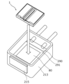
- Fig. 23 is a schematic perspective view showing the overall configuration of a light-emitting module 206 according to the present embodiment.
- the light emitting module 206 includes a module substrate 290, a frame 213, a light-transmitting window 215, a light emitting device 1, and two current input terminals 240.
- the light emitting device 1 according to this embodiment also includes a semiconductor laser element 10, a base 70, and a first bonding layer 30, similar to the first embodiment.
- the module substrate 290 is a plate-like member that serves as the base for the light-emitting module 206.
- the module substrate 290 is made of a material with high thermal conductivity, such as Cu or Al.
- the module substrate 290 corresponds to the heat sink in the first embodiment.
- the frame body 213 is an annular side wall that is erected on the module substrate 290.
- a through hole (not shown) is formed in the frame body 213, penetrating a portion of the frame body 213 in a direction along the top surface of the module substrate 290.
- This through hole is a through hole for extracting laser light emitted from the light-emitting device 1 arranged inside the frame body 213 to the outside of the frame body 213.
- the through hole is covered with a light-transmitting window 215.
- the frame body 213 is made of an Fe-based material, such as Fe, an FeNi alloy, or stainless steel.
- the light-emitting module 206 is disposed on the frame body 213 and has a plate-shaped lid that covers the opening of the frame body 213 (see the lid 214 shown in FIG. 25 described later).
- the lid is made of an Fe-based material such as Fe, an FeNi alloy, or stainless steel.
- the module substrate 290, the frame body 213, and the lid form a housing.
- the light-emitting device 1 is disposed inside the housing.
- the light-transmitting window 215 is a window for extracting the laser light emitted from the light-emitting device 1 to the outside of the frame body 213.
- the light-transmitting window 215 is made of, for example, glass. It is a plate-shaped member.
- the current introduction terminals 240 are terminals for introducing current from the outside of the frame body 213 to the inside of the frame body 213. One end of each of the two current introduction terminals 240 is disposed outside the frame body 213, and the other end is disposed inside the frame body 213. In this embodiment, the current introduction terminals 240 are disposed in the frame body 213 and penetrate the frame body 213. If the frame body 213 is formed of a conductive material, an insulating member is disposed between the current introduction terminals 240 and the frame body 213. The current introduction terminals 240 and the light-emitting device 1 are electrically connected by a metal wire (not shown).
- FIG. 24 and Fig. 25 are schematic perspective views showing each step of the method for manufacturing the light emitting module 206 according to the present embodiment.
- a frame 213 on which a current introduction terminal 240 is arranged is placed on a module substrate 290.
- the through hole of the frame 213 is covered by a light-transmitting window 215.
- the module substrate 290 also has a flat laser mounting surface 291, and the second bonding layer 80 is placed on the laser mounting surface 291.
- the light-emitting device 1 is placed on the second bonding layer 80.
- the light-emitting device 1 is placed on the laser mounting surface 291, and the module substrate 290 is heated while the light-emitting device 1 is pressed against the laser mounting surface 291.
- the second bonding layer 80 is melted by heating at 300°C for about 1 minute.
- the light emitting device 1 can be bonded to the laser mounting surface 291 by the second bonding layer 80.
- a solder made of AuSn is used as the second bonding layer 80.
- the light-emitting device 1 and the two current input terminals 140 are connected by wire bonding.
- the module substrate 290 to which the light-emitting device 1 and other components are bonded and the lid 214 are placed in an ozone atmosphere for a predetermined period of time. This removes organic matter adhering to the surfaces of the module substrate 290 and each component bonded to the module substrate 290.
- the inside of the frame 213 is immediately hermetically sealed. Specifically, for example, the module substrate 290 to which the light emitting device 1 and the like are joined, and the lid 214 are placed in a clean, dry air atmosphere. Next, the lid 214 is joined to the upper surface of the frame 213 by seam welding.
- the light-emitting module 206 according to this embodiment can be manufactured.
- components such as the light-emitting device 1 are sealed in the internal space of the light-emitting module 206, which is filled with clean, dry air. This allows the light-emitting device 1 in the light-emitting module 206 and the surface facing the through-hole of the translucent window 215 to be kept clean.
- the light-emitting device 1 since the light-emitting device 1 is hermetically sealed, it is possible to prevent foreign matter such as organic matter from being adsorbed near the light-emitting portion of the semiconductor laser element 10 due to the optical tweezers effect while the light-emitting device 1 is emitting light. This makes it possible to realize a highly reliable light-emitting module 206.
- the light-emitting device 1 is fixed to a heat sink made of a module substrate 290. This makes it possible to exhaust Joule heat generated in the hermetically sealed light-emitting device 1 to the outside of the light-emitting module 206 through the heat sink.
- the semiconductor laser element 10 and the base 70 are connected by a first bonding layer 30 with high thermal conductivity. Therefore, it is possible to efficiently exhaust Joule heat generated in the semiconductor laser element 10 to the outside of the light-emitting module 206 through the heat sink.
- a light emitting module according to a modified example of the present embodiment will be described.
- the light emitting module according to this modified example differs from the light emitting module 206 according to the present embodiment described above mainly in the direction of emission of the laser light.
- the light emitting module according to this modified example will be described below, focusing on the differences from the light emitting module 206 according to the present embodiment.
- Fig. 26 is a schematic cross-sectional view showing the overall configuration of a light emitting module 506 according to this modification. A cross section parallel to the optical axis of the laser light emitted by the light emitting module 506 is shown.
- the light emitting module 506 includes a module substrate 590, a frame 513, a lid 514, a light-transmitting window 515, a light emitting device 1, a second bonding layer 80, a reflecting mirror 522, an optical element bonding layer 581, and a current input terminal 540.
- the light emitting device 1 according to this embodiment also includes a semiconductor laser element 10, a base 70, and a first bonding layer 30, similar to the first embodiment.
- the module substrate 590 is a plate-like member that serves as the base for the light-emitting module 506.
- the module substrate 590 is made of a material with high thermal conductivity, such as Cu or Al.
- the module substrate 590 corresponds to the heat sink in the first embodiment.
- the frame 513 is an annular side wall that is erected on the module substrate 590.
- the frame 513 is made of an Fe-based material, such as Fe, an FeNi alloy, or stainless steel.
- the lid 514 is a plate-like member that covers the opening of the frame 513.
- the lid 514 is made of an Fe-based material, such as Fe, an FeNi alloy, or stainless steel.
- a through hole is formed in the lid 514. This through hole is a through hole for extracting laser light emitted from the light-emitting device 1 arranged in the area surrounded by the lid 514, the frame 513, and the module substrate 590 to the outside of the area.
- the through hole is covered by a light-transmitting window 515.
- the second bonding layer 80 bonds the base 70 of the light-emitting device 1 to the heat sink, similar to the second bonding layer 80 in the first embodiment. In this modification, the second bonding layer 80 bonds the base 70 to the module substrate 590.
- the reflecting mirror 522 is an optical element that changes the traveling direction of the laser light emitted from the semiconductor laser element 10 of the light-emitting device 1.
- the reflecting mirror 522 has a reflecting surface that is inclined at 45 degrees with respect to the main surface of the module substrate 590.
- the reflecting mirror 522 reflects the laser light traveling parallel to the main surface of the module substrate 590, thereby bending the traveling direction of the laser light by 90 degrees to a direction perpendicular to the main surface of the module substrate 590.
- the laser light reflected upward in FIG. 26 by the reflecting mirror 522 passes through the light-transmitting window 515 arranged in the through hole of the lid 514, and is output to the outside of the light-emitting module 506.
- the optical element bonding layer 581 is a bonding member that bonds the module substrate 590 and the reflecting mirror 522.
- the optical element bonding layer 581 is disposed between the module substrate 590 and the reflecting mirror 522.
- a material with a relatively high melting point can be selected for the optical element bonding layer 581, similar to the second bonding layer 80.
- AuSn, SnAgCu, etc. can be used for the optical element bonding layer 581, and the reflecting mirror 522 and the module substrate 590 can be firmly bonded together.
- the current introduction terminal 540 is a terminal for introducing a current from the outside of the frame body 513 to the inside of the frame body 513.
- the light-emitting module 506 may be provided with two current introduction terminals 540. One end of each of the current introduction terminals 540 is disposed outside the frame body 513, and the other end is disposed inside the frame body 513. In this modification, the current introduction terminal 540 is disposed in the frame body 513 and penetrates the frame body 513. If the frame body 513 is formed of a conductive material, an insulating member is disposed between the current introduction terminal 540 and the frame body 513.
- the current introduction terminal 540 and the semiconductor laser element 10 of the light-emitting device 1 are connected by a wire W.
- the light-emitting device 1 can be mounted on the module substrate 590 so that the resonance direction of the semiconductor laser element 10 is parallel to the main surface of the module substrate 590, and laser light can be emitted in a direction perpendicular to the main surface of the module substrate 590.
- a method for manufacturing the light emitting module 506 according to this modification will be described.
- the method for manufacturing the light emitting module 506 according to this modification differs from the method for manufacturing the light emitting module 206 according to the third embodiment in that it includes a step of bonding the reflection mirror 522 to the module substrate 590.
- the reflecting mirror 522 may be bonded to the module substrate 590 in the process of bonding the light emitting device 1 to the module substrate 590. That is, the light emitting device 1 and the reflecting mirror 522 may be bonded to the main surface of the module substrate 590 as follows. First, the second bonding layer 80 and the optical element bonding layer 581 are disposed on the main surface of the module substrate 590. Next, the light emitting device 1 is disposed on the second bonding layer 80, and the reflecting mirror 522 is disposed on the optical element bonding layer 581. Next, the module substrate 590 is heated while pressing the light emitting device 1 and the reflecting mirror 522 against the module substrate 590.
- the second bonding layer 80 and the optical element bonding layer 581 are melted by heating at 300°C for about one minute.
- the light emitting device 1 and the reflective mirror 522 can be bonded to the module substrate 590 by the second bonding layer 80 and the optical element bonding layer 581.
- the reflecting mirror 522 is bonded to the module substrate 590 in a separate process from the process of bonding the light emitting device 1 to the module substrate 590.
- a material having a lower melting point than the second bonding layer 80 is selected as the optical element bonding layer 581.
- AuSn solder is used as the second bonding layer 80
- SnAgCu solder or the like can be used as the optical element bonding layer 581.
- the reflecting mirror 522 can be precisely aligned with respect to the light emitting device 1. It is also possible to align the reflecting mirror 522 while emitting laser light from the light emitting device 1.
- the light-emitting module 506 according to this modified example can be manufactured.
- the light-emitting device 1 and the reflecting mirror 522 are fixed with an inorganic material and then hermetically sealed. This makes it possible to realize a highly reliable light-emitting module 506.
- Embodiment 4 A light emitting device and a light emitting module according to embodiment 4 will be described.
- the light emitting device according to this embodiment differs from the light emitting device 1 according to embodiment 1 mainly in the configuration of the metal film.
- the light emitting device and the light emitting module according to this embodiment will be described below with reference to FIG. 27, focusing on the differences from the light emitting device 1 and the light emitting module 5 according to embodiment 1.
- FIG. 27 is a schematic cross-sectional view showing the overall configuration of the light-emitting module 305 according to this embodiment.
- FIG. 27 shows a cross section perpendicular to the propagation direction of the light emitted by the light-emitting module 305.
- the light-emitting module 305 of this embodiment includes a light-emitting device 301, a heat sink 90, a second bonding layer 80, and a wire W.
- the light-emitting device 301 according to this embodiment differs from the light-emitting device 1 according to the first embodiment shown in FIG. 2 in the configuration of the metal film 350, but is the same in other respects.
- the metal film 350 has an extension 350e that extends outward from the side surface of the semiconductor laser element 10 (i.e., the side surface 10Sc of the semiconductor laminate 10S) in a direction perpendicular to the resonance direction of the semiconductor laser element 10 and the stacking direction of the first bonding layer 30.
- the detailed configuration of the extension 350e will be described later.
- the wire W is an example of a power supply conductor for supplying power to the semiconductor laser element 10 included in the light-emitting device 301.
- a wire W which is an example of a power supply conductor for supplying power to the semiconductor laser element 10
- the extension 350e and the power supply conductor are bonded without any other conductive member included in the light-emitting module 305 being interposed between them.
- the wire W is directly bonded to the extension 350e.
- power can be supplied directly to the metal film 350 without going through the base electrode 60, so that the electrical resistance of the light-emitting module 305 can be reduced. Therefore, the ohmic loss and heat generation in the base electrode 60 can be reduced.
- Such a configuration is particularly effective when the current supplied to the semiconductor laser element 10 is large.
- the thickness of the metal film 350 may be 3 ⁇ m or more. This can further reduce the electrical resistance of the light-emitting module 305.
- the width of the extension 350e (the horizontal dimension in FIG. 27) may be 50 ⁇ m or more. This makes it easier to join the power supply conductor to the extension 350e.
- At least a portion of the surface of the extension portion 350e behind the surface facing the base body 70 may be flat. This makes it easier to join the power supply conductor to the extension portion 350e.
- Embodiment 5 A light emitting device and a light emitting module according to embodiment 5 will be described.
- the light emitting device according to this embodiment differs from the light emitting device 1 according to embodiment 1 mainly in the configuration of the base bonding layer.
- the light emitting device and the light emitting module according to this embodiment will be described below with reference to FIG. 28, focusing on the differences from the light emitting device 1 and the light emitting module 5 according to embodiment 1.
- FIG. 28 is a schematic cross-sectional view showing the overall configuration of the light-emitting module 405 according to this embodiment.
- FIG. 28 shows a cross section perpendicular to the propagation direction of the light emitted by the light-emitting module 405.
- the light-emitting module 405 of this embodiment includes a light-emitting device 401, a heat sink 90, a second bonding layer 80, and a wire W.
- the light-emitting device 401 according to this embodiment differs from the light-emitting device 1 according to the first embodiment shown in FIG. 2 in the configuration of the base electrode 460 and relay electrode 471, but is the same in other respects.
- the substrate electrode 460 according to this embodiment has a substrate adhesion layer 61 and a substrate bonding layer 462.
- the substrate bonding layer 462 according to this embodiment differs from the substrate bonding layer 62 according to embodiment 1 in that it has a thickness of 0.3 ⁇ m or more, but is the same in other respects.
- the relay electrode 471 according to this embodiment has a substrate adhesion layer 72 and a pad electrode layer 473.
- the pad electrode layer 473 according to this embodiment differs from the pad electrode layer 73 according to embodiment 1 in that the thickness of the pad electrode layer 473 according to this embodiment is 0.3 ⁇ m or more, but is the same in other respects.
- a wire W which is an example of a power supply conductor for supplying power to the semiconductor laser element 10, is directly bonded to the base bonding layer 462.
- the electrical resistance in the direction perpendicular to the thickness direction of the base bonding layer 462 can be reduced. Therefore, by directly bonding the wire W to the base bonding layer 462, the electrical resistance in the current path from the wire W to the metal film 50 can be reduced. This reduces the ohmic loss and heat generation in the base bonding layer 462. This configuration is particularly effective when the current supplied to the semiconductor laser element 10 is large.
- the thickness of the substrate bonding layer 462 may be 3 ⁇ m or more. This can further reduce the electrical resistance in the direction perpendicular to the thickness direction of the substrate bonding layer 462.
- the thickness of the pad electrode layer 473 of the relay electrode 471 be 0.3 ⁇ m or more, the electrical resistance in the direction perpendicular to the thickness direction of the pad electrode layer 473 can be reduced. Therefore, for example, as shown in FIG. 28, when multiple wires W are joined to the pad electrode layer 473 to relay a current path, the electrical resistance in the pad electrode layer 473 can be reduced. This makes it possible to reduce ohmic loss and heat generation in the pad electrode layer 473.
- the thickness of the pad electrode layer 473 may be 3 ⁇ m or more. This can further reduce the electrical resistance in a direction perpendicular to the thickness direction of the pad electrode layer 473.
- FIG. 6 is a schematic cross-sectional view showing the overall configuration of a light emitting module 505 according to this embodiment.
- the light-emitting module 505 of this embodiment includes a light-emitting device 501, a heat sink 90, and a second bonding layer 80.
- the light-emitting device 501 includes a semiconductor laser element 10, a first electrode 20, a base 570, a first bonding layer 530, a relay electrode 571, and a back metal layer 576.
- the base 570 is a base to which the semiconductor laser element 10 is bonded.
- the base 570 has a first main surface 570a to which the semiconductor laser element 10 is bonded, and a second main surface 570b located on the back side of the first main surface 570a.
- the base 570 is made of an electrically insulating material. More specifically, the base 570 is an AlN ceramic substrate having a thickness of 350 ⁇ m.
- the first bonding layer 530 has a second electrode 40, a metal film 50, and a substrate electrode 560, which are arranged in this order from the semiconductor laser element 10 toward the substrate 570.
- the substrate electrode 560 is a conductive member disposed between the metal film 50 and the substrate 570.
- the substrate electrode 560 is disposed on the first main surface 570a of the substrate 570.
- the substrate electrode 560 has a substrate bonding layer 562a, a substrate adhesion layer 561b, a substrate bonding layer 562b, and a substrate adhesion layer 561a, which are disposed in this order from the semiconductor laser element 10 toward the substrate 570.
- the substrate adhesion layer 561a is a conductive layer disposed between the substrate 570 and the substrate bonding layer 562b. In this embodiment, the substrate adhesion layer 561a contacts the first main surface 570a of the substrate 570.
- the substrate adhesion layer 561a may have a function of increasing the adhesion between the first main surface 570a of the substrate 570 and the substrate bonding layer 562b.
- the substrate adhesion layer 561a may be, for example, a single layer film made of Ti, Cr, or Ni. In this embodiment, the substrate adhesion layer 561a is a Ti film having a thickness of 0.1 ⁇ m.
- the substrate bonding layer 562b is disposed between the metal film 50 and the substrate 570, and is a conductive layer made of a single metal element.
- the substrate bonding layer 562b is disposed between the substrate adhesion layer 561a and the substrate adhesion layer 561b.
- the substrate bonding layer 562b may be selected from Au, Ag, Cu, or Al.
- the thickness of the substrate bonding layer 562b may be, for example, 10 ⁇ m or more, 30 ⁇ m or more, or 50 ⁇ m or more.
- the substrate bonding layer 562b is a Cu film having a thickness of 75 ⁇ m.
- the thickness of the base bonding layer 562b is increased in this way, warping of the base 570 due to the difference in thermal expansion coefficient between the base bonding layer 562b and the base 570 may become significant.
- a film having the same configuration as the base bonding layer 562b may be formed on the second main surface 570b of the base 570, or a back metal layer 576 having the same layer configuration as the base electrode 560 may be disposed on the second main surface 570b of the base 570.
- the base bonding layer 562b may be formed by plating, such as electrolytic plating, for example.
- the substrate adhesion layer 561b is a conductive layer disposed between the substrate 570 and the substrate bonding layer 562a. In this embodiment, the substrate adhesion layer 561b is disposed between the substrate bonding layer 562a and the substrate bonding layer 562b. The substrate adhesion layer 561b may have a function of increasing the adhesion between the substrate bonding layer 562a and the substrate bonding layer 562b.
- the substrate adhesion layer 561b may be, for example, a single layer film made of Ti, Cr, or Ni. In this embodiment, the substrate adhesion layer 561b is a Ni film having a thickness of 1 ⁇ m.
- the substrate bonding layer 562a is disposed between the metal film 50 and the substrate 570, and is a conductive layer made of a single metal element. In this embodiment, the substrate bonding layer 562a is disposed between the substrate adhesion layer 561b and the metal film 50.
- the substrate bonding layer 562a may be selected from Au, Ag, Cu, or Al. In this embodiment, the substrate bonding layer 562a is an Au film having a thickness of 1 ⁇ m.
- the relay electrode 571 is a conductive member disposed on the base 570.
- the relay electrode 571 is electrically insulated from the base electrode 560.
- the relay electrode 571 is disposed on the first main surface 570a of the base 570.
- the relay electrode 571 may be used to relay a power supply path for supplying power to the first electrode 20. For example, as shown in FIG. 29, a wire W connected to a power source (not shown) and a wire W connected to the first electrode 20 may be bonded to the relay electrode 571.
- the relay electrode 571 has a base adhesion layer 572a arranged on the first main surface 570a of the base 570, a pad electrode layer 573b arranged above the base adhesion layer 572a, a base adhesion layer 572b arranged above the pad electrode layer 573b, and a pad electrode layer 573a arranged above the base adhesion layer 572b.
- the base adhesion layer 572a is arranged between the base 570 and the pad electrode layer 573b.
- the pad electrode layer 573b is arranged between the base adhesion layer 572a and the base adhesion layer 572b.
- the base adhesion layer 572b is arranged between the pad electrode layer 573b and the pad electrode layer 573a.
- the pad electrode layer 573a is arranged above the base adhesion layer 572b.
- the relay electrode 571 may have the same layer structure as the base electrode 560.
- the relay electrode 571 may also be formed at the same time as the base electrode 560 in the same process.
- the back metal layer 576 is a metal layer disposed on the second main surface 570b of the base 570.
- the back metal layer 576 may have the function of increasing the adhesion between the base 570 and the heat sink 90.
- the back metal layer 576 has a back adhesion layer 577a, a back bonding layer 578b, a back adhesion layer 577b, and a back bonding layer 578a.
- the back metal layer 576 may have the same layer structure as the base electrode 560.
- the back adhesion layer 577a is a metal layer disposed between the substrate 570 and the back adhesion layer 578b. In this embodiment, the back adhesion layer 577a contacts the second main surface 570b of the substrate 570.
- the back adhesion layer 577a may have a function of increasing the adhesion between the second main surface 570b of the substrate 570 and the back adhesion layer 578b.
- the back adhesion layer 577a may be, for example, a single layer film made of Ti, Cr, or Ni. In this embodiment, the back adhesion layer 577a is a Ti film having a thickness of 0.1 ⁇ m.
- the back surface bonding layer 578b is a conductive layer disposed between the substrate 570 and the second bonding layer 80. In this embodiment, the back surface bonding layer 578b is disposed between the back surface adhesive layer 577a and the back surface adhesive layer 577b.
- the back surface bonding layer 578b is a layer made of a single metal element.
- the back surface bonding layer 578b may be a single layer film made of Au, Ag, Cu, or Al.
- the back surface bonding layer 578b is a single layer film made of Cu.
- the back surface bonding layer 578b is a Cu film having a thickness of 75 ⁇ m.
- the back surface bonding layer 578b may be formed by plating, for example.
- the back adhesion layer 577b is a metal layer disposed between the substrate 570 and the back adhesion layer 578a. In this embodiment, the back adhesion layer 577b is disposed between the back adhesion layer 578b and the back adhesion layer 578a. The back adhesion layer 577b may have a function of increasing the adhesion between the back adhesion layer 578b and the back adhesion layer 578a.
- the back adhesion layer 577b may be, for example, a single layer film made of Ti, Cr, or Ni. In this embodiment, the back adhesion layer 577b is a Ni film having a thickness of 1 ⁇ m.
- the back surface bonding layer 578a is a conductive layer disposed between the substrate 570 and the second bonding layer 80. In this embodiment, the back surface bonding layer 578a is disposed between the back surface adhesive layer 577b and the second bonding layer 80.
- the back surface bonding layer 578a is a layer made of a single metal element.
- the back surface bonding layer 578a may be a single layer film made of Au, Ag, Cu, or Al.
- the back surface bonding layer 578a is a single layer film made of Au.
- the back surface bonding layer 578a is an Au film having a thickness of 1 ⁇ m.
- the light emitting module 505 having the above configuration also achieves the same effects as the light emitting module 5 according to embodiment 1. Furthermore, in this embodiment, since the thick substrate bonding layer 562b is made of Au, Ag, Cu, or Al, which has a high thermal conductivity, the heat dissipation of the substrate electrode 560 in the direction along the first main surface 570a of the substrate 570 can be improved. Furthermore, the electrical resistance in the direction along the first main surface 570a of the substrate electrode 560 can be reduced.
- FIG. 7 is a schematic cross-sectional view showing the overall configuration of a light-emitting module 605 according to this embodiment.
- the light-emitting module 605 of this embodiment includes a light-emitting device 601, a second bonding layer 80, and a heat sink 90.
- the light-emitting device 601 includes a semiconductor laser element 10, a first electrode 20, a substrate 70, a first bonding layer 30, a Zener diode 699, a functional element bonding layer 651, and a back metal layer 76.
- the Zener diode 699 is an example of a functional element having a different function from the semiconductor laser element 10.
- the Zener diode 699 is connected in inverse parallel to the semiconductor laser element 10, for example. That is, the cathode electrode 699a of the Zener diode 699 is connected to the anode of the semiconductor laser element 10, and the anode electrode 699b of the Zener diode 699 is connected to the cathode of the semiconductor laser element 10.
- a Zener diode 699 having a breakdown voltage slightly higher than the operating voltage of the semiconductor laser element 10 is used.
- a voltage less than the breakdown voltage of the Zener diode 699 is applied to the semiconductor laser element 10, a current flows only through the semiconductor laser element 10.
- the Zener diode 699 when a voltage equal to or greater than the breakdown voltage of the Zener diode 699 is applied to the semiconductor laser element 10 due to a surge or the like, the Zener diode 699 has a lower resistance than the semiconductor laser element 10, so that a current flows only through the Zener diode 699. Furthermore, when a reverse voltage is applied to the semiconductor laser element 10, a forward voltage is applied to the Zener diode 699, so that a current flows only through the Zener diode 699. As described above, the Zener diode 699 has the function of protecting the semiconductor laser element 10 when an abnormal voltage is applied to the semiconductor laser element 10.
- the Zener diode 699 is disposed on the first main surface 70a of the base 70.
- the cathode electrode 699a of the Zener diode 699 is bonded to the base electrode 60 by the functional element bonding layer 651.
- the Zener diode 699 is disposed on the first main surface 70a of the base 70 via the base electrode 60 and the functional element bonding layer 651. Note that since the Zener diode 699 does not need to be precisely aligned with the semiconductor laser element 10, it may be bonded to the semiconductor laser element 10 at the same time by the functional element bonding layer 651 having a configuration similar to that of the metal film 50.
- the functional element bonding layer 651 is a member that bonds the base 70 and the functional element.
- the functional element bonding layer 651 has a configuration similar to that of the metal film 50.
- the light emitting module 605 having the above configuration also achieves the same effects as the light emitting module 5 according to the first embodiment. Furthermore, in this embodiment, the light emitting module 605 includes a functional element, so that a function can be added to the light emitting module 5.
- the light emitting module 605 according to this embodiment includes a Zener diode 699 as a functional element, so that the semiconductor laser element 10 can be protected when an abnormal voltage is applied to the semiconductor laser element 10.
- the paste 50P is patterned when it is applied, but it may be patterned after application.
- wire W is used as the power supply conductor
- the configuration of the power supply conductor is not limited to this.
- a plate-shaped, rod-shaped, or sheet-shaped conductor may be used as the power supply conductor, or a conductive film disposed on a wiring board may be used.
- a power supply conductor may be directly bonded to the extension of the metal film, and another power supply conductor may be directly bonded to the substrate bonding layer.
- the light-emitting devices disclosed herein are particularly useful as high-brightness, high-power laser light sources, such as laser light sources for processing, laser light sources for displays, and medical laser light sources.
Landscapes
- Physics & Mathematics (AREA)
- Condensed Matter Physics & Semiconductors (AREA)
- General Physics & Mathematics (AREA)
- Electromagnetism (AREA)
- Optics & Photonics (AREA)
- Geometry (AREA)
- Semiconductor Lasers (AREA)
Priority Applications (1)
| Application Number | Priority Date | Filing Date | Title |
|---|---|---|---|
| JP2024574457A JPWO2024162073A1 (https=) | 2023-01-30 | 2024-01-22 |
Applications Claiming Priority (2)
| Application Number | Priority Date | Filing Date | Title |
|---|---|---|---|
| JP2023011751 | 2023-01-30 | ||
| JP2023-011751 | 2023-01-30 |
Publications (1)
| Publication Number | Publication Date |
|---|---|
| WO2024162073A1 true WO2024162073A1 (ja) | 2024-08-08 |
Family
ID=92146557
Family Applications (1)
| Application Number | Title | Priority Date | Filing Date |
|---|---|---|---|
| PCT/JP2024/001685 Ceased WO2024162073A1 (ja) | 2023-01-30 | 2024-01-22 | 発光デバイス、発光モジュール、発光デバイスの製造方法、及び、発光モジュールの製造方法 |
Country Status (2)
| Country | Link |
|---|---|
| JP (1) | JPWO2024162073A1 (https=) |
| WO (1) | WO2024162073A1 (https=) |
Citations (5)
| Publication number | Priority date | Publication date | Assignee | Title |
|---|---|---|---|---|
| JP2004265961A (ja) * | 2003-02-28 | 2004-09-24 | Furukawa Electric Co Ltd:The | 半導体レーザ装置、半導体レーザモジュールおよび半導体レーザ装置の製造方法 |
| JP2004281863A (ja) * | 2003-03-18 | 2004-10-07 | Nichia Chem Ind Ltd | 窒化物半導体素子及びその製造方法 |
| WO2020174982A1 (ja) * | 2019-02-27 | 2020-09-03 | パナソニックセミコンダクターソリューションズ株式会社 | 半導体レーザモジュール |
| WO2021235304A1 (ja) * | 2020-05-21 | 2021-11-25 | ソニーグループ株式会社 | 半導体レーザ素子及び半導体レーザ素子の製造方法 |
| JP2022089985A (ja) * | 2019-01-10 | 2022-06-16 | 三菱電機株式会社 | 半導体レーザ装置 |
-
2024
- 2024-01-22 JP JP2024574457A patent/JPWO2024162073A1/ja active Pending
- 2024-01-22 WO PCT/JP2024/001685 patent/WO2024162073A1/ja not_active Ceased
Patent Citations (5)
| Publication number | Priority date | Publication date | Assignee | Title |
|---|---|---|---|---|
| JP2004265961A (ja) * | 2003-02-28 | 2004-09-24 | Furukawa Electric Co Ltd:The | 半導体レーザ装置、半導体レーザモジュールおよび半導体レーザ装置の製造方法 |
| JP2004281863A (ja) * | 2003-03-18 | 2004-10-07 | Nichia Chem Ind Ltd | 窒化物半導体素子及びその製造方法 |
| JP2022089985A (ja) * | 2019-01-10 | 2022-06-16 | 三菱電機株式会社 | 半導体レーザ装置 |
| WO2020174982A1 (ja) * | 2019-02-27 | 2020-09-03 | パナソニックセミコンダクターソリューションズ株式会社 | 半導体レーザモジュール |
| WO2021235304A1 (ja) * | 2020-05-21 | 2021-11-25 | ソニーグループ株式会社 | 半導体レーザ素子及び半導体レーザ素子の製造方法 |
Also Published As
| Publication number | Publication date |
|---|---|
| JPWO2024162073A1 (https=) | 2024-08-08 |
Similar Documents
| Publication | Publication Date | Title |
|---|---|---|
| JP4897133B2 (ja) | 半導体発光素子、その製造方法および配設基板 | |
| CN104040809B (zh) | 半导体激光器装置以及其制造方法 | |
| US8031751B2 (en) | Nitride semiconductor laser device | |
| US9735314B2 (en) | Nitride semiconductor light emitting device | |
| CN1299170A (zh) | 制造半导体激光器的方法及安装板和支撑板 | |
| JP2003031895A (ja) | 半導体発光装置およびその製造方法 | |
| JP2016054279A (ja) | 半導体レーザ | |
| US9780523B2 (en) | Semiconductor laser device | |
| JP2015513229A (ja) | レーザーダイオード装置 | |
| US8138663B2 (en) | Light emitting device and method of manufacturing the same | |
| JP7583321B2 (ja) | 光源装置 | |
| CN118613976A (zh) | 激光器封装件和用于制造激光器封装件的方法 | |
| JP4573882B2 (ja) | 半導体レーザ装置 | |
| JPH10308560A (ja) | 半導体発光素子および発光装置 | |
| JP5245980B2 (ja) | 発光装置及びその製造方法 | |
| WO2024162073A1 (ja) | 発光デバイス、発光モジュール、発光デバイスの製造方法、及び、発光モジュールの製造方法 | |
| CN111541144A (zh) | 半导体激光光源装置 | |
| US7873086B2 (en) | Semiconductor device | |
| JP7783486B2 (ja) | 発光装置 | |
| JP7271243B2 (ja) | レーザ装置及びそれに用いる蓋体 | |
| WO2024162074A1 (ja) | 半導体レーザデバイス、半導体レーザ素子用サブマウント、半導体レーザ素子用集合サブマウント、発光デバイスの製造方法、及び発光素子用サブマウントの製造方法 | |
| JP2024104058A (ja) | 発光素子及び発光装置 | |
| JP2008010597A (ja) | 半導体発光素子接合体およびサブマウント | |
| JP2008130664A (ja) | 半導体発光素子および発光装置 | |
| JP2004039926A (ja) | 半導体レーザ装置及びその製造方法 |
Legal Events
| Date | Code | Title | Description |
|---|---|---|---|
| 121 | Ep: the epo has been informed by wipo that ep was designated in this application |
Ref document number: 24750025 Country of ref document: EP Kind code of ref document: A1 |
|
| ENP | Entry into the national phase |
Ref document number: 2024574457 Country of ref document: JP Kind code of ref document: A |
|
| WWE | Wipo information: entry into national phase |
Ref document number: 2024574457 Country of ref document: JP |
|
| NENP | Non-entry into the national phase |
Ref country code: DE |
|
| 122 | Ep: pct application non-entry in european phase |
Ref document number: 24750025 Country of ref document: EP Kind code of ref document: A1 |