WO2024157830A1 - Method for fabricating piezoelectric film, piezoelectric film fabricated using said method, and piezoelectric device - Google Patents
Method for fabricating piezoelectric film, piezoelectric film fabricated using said method, and piezoelectric device Download PDFInfo
- Publication number
- WO2024157830A1 WO2024157830A1 PCT/JP2024/000878 JP2024000878W WO2024157830A1 WO 2024157830 A1 WO2024157830 A1 WO 2024157830A1 JP 2024000878 W JP2024000878 W JP 2024000878W WO 2024157830 A1 WO2024157830 A1 WO 2024157830A1
- Authority
- WO
- WIPO (PCT)
- Prior art keywords
- piezoelectric
- piezoelectric film
- film
- crystal axis
- substrate
- Prior art date
- Legal status (The legal status is an assumption and is not a legal conclusion. Google has not performed a legal analysis and makes no representation as to the accuracy of the status listed.)
- Ceased
Links
Images







Classifications
-
- H—ELECTRICITY
- H10—SEMICONDUCTOR DEVICES; ELECTRIC SOLID-STATE DEVICES NOT OTHERWISE PROVIDED FOR
- H10N—ELECTRIC SOLID-STATE DEVICES NOT OTHERWISE PROVIDED FOR
- H10N30/00—Piezoelectric or electrostrictive devices
- H10N30/01—Manufacture or treatment
- H10N30/09—Forming piezoelectric or electrostrictive materials
- H10N30/093—Forming inorganic materials
-
- C—CHEMISTRY; METALLURGY
- C23—COATING METALLIC MATERIAL; COATING MATERIAL WITH METALLIC MATERIAL; CHEMICAL SURFACE TREATMENT; DIFFUSION TREATMENT OF METALLIC MATERIAL; COATING BY VACUUM EVAPORATION, BY SPUTTERING, BY ION IMPLANTATION OR BY CHEMICAL VAPOUR DEPOSITION, IN GENERAL; INHIBITING CORROSION OF METALLIC MATERIAL OR INCRUSTATION IN GENERAL
- C23C—COATING METALLIC MATERIAL; COATING MATERIAL WITH METALLIC MATERIAL; SURFACE TREATMENT OF METALLIC MATERIAL BY DIFFUSION INTO THE SURFACE, BY CHEMICAL CONVERSION OR SUBSTITUTION; COATING BY VACUUM EVAPORATION, BY SPUTTERING, BY ION IMPLANTATION OR BY CHEMICAL VAPOUR DEPOSITION, IN GENERAL
- C23C14/00—Coating by vacuum evaporation, by sputtering or by ion implantation of the coating forming material
- C23C14/06—Coating by vacuum evaporation, by sputtering or by ion implantation of the coating forming material characterised by the coating material
- C23C14/08—Oxides
-
- C—CHEMISTRY; METALLURGY
- C30—CRYSTAL GROWTH
- C30B—SINGLE-CRYSTAL GROWTH; UNIDIRECTIONAL SOLIDIFICATION OF EUTECTIC MATERIAL OR UNIDIRECTIONAL DEMIXING OF EUTECTOID MATERIAL; REFINING BY ZONE-MELTING OF MATERIAL; PRODUCTION OF A HOMOGENEOUS POLYCRYSTALLINE MATERIAL WITH DEFINED STRUCTURE; SINGLE CRYSTALS OR HOMOGENEOUS POLYCRYSTALLINE MATERIAL WITH DEFINED STRUCTURE; AFTER-TREATMENT OF SINGLE CRYSTALS OR A HOMOGENEOUS POLYCRYSTALLINE MATERIAL WITH DEFINED STRUCTURE; APPARATUS THEREFOR
- C30B29/00—Single crystals or homogeneous polycrystalline material with defined structure characterised by the material or by their shape
- C30B29/10—Inorganic compounds or compositions
- C30B29/16—Oxides
- C30B29/22—Complex oxides
- C30B29/32—Titanates; Germanates; Molybdates; Tungstates
-
- C—CHEMISTRY; METALLURGY
- C30—CRYSTAL GROWTH
- C30B—SINGLE-CRYSTAL GROWTH; UNIDIRECTIONAL SOLIDIFICATION OF EUTECTIC MATERIAL OR UNIDIRECTIONAL DEMIXING OF EUTECTOID MATERIAL; REFINING BY ZONE-MELTING OF MATERIAL; PRODUCTION OF A HOMOGENEOUS POLYCRYSTALLINE MATERIAL WITH DEFINED STRUCTURE; SINGLE CRYSTALS OR HOMOGENEOUS POLYCRYSTALLINE MATERIAL WITH DEFINED STRUCTURE; AFTER-TREATMENT OF SINGLE CRYSTALS OR A HOMOGENEOUS POLYCRYSTALLINE MATERIAL WITH DEFINED STRUCTURE; APPARATUS THEREFOR
- C30B29/00—Single crystals or homogeneous polycrystalline material with defined structure characterised by the material or by their shape
- C30B29/10—Inorganic compounds or compositions
- C30B29/38—Nitrides
-
- H—ELECTRICITY
- H10—SEMICONDUCTOR DEVICES; ELECTRIC SOLID-STATE DEVICES NOT OTHERWISE PROVIDED FOR
- H10N—ELECTRIC SOLID-STATE DEVICES NOT OTHERWISE PROVIDED FOR
- H10N30/00—Piezoelectric or electrostrictive devices
- H10N30/01—Manufacture or treatment
- H10N30/07—Forming of piezoelectric or electrostrictive parts or bodies on an electrical element or another base
- H10N30/074—Forming of piezoelectric or electrostrictive parts or bodies on an electrical element or another base by depositing piezoelectric or electrostrictive layers, e.g. aerosol or screen printing
- H10N30/076—Forming of piezoelectric or electrostrictive parts or bodies on an electrical element or another base by depositing piezoelectric or electrostrictive layers, e.g. aerosol or screen printing by vapour phase deposition
-
- H—ELECTRICITY
- H10—SEMICONDUCTOR DEVICES; ELECTRIC SOLID-STATE DEVICES NOT OTHERWISE PROVIDED FOR
- H10N—ELECTRIC SOLID-STATE DEVICES NOT OTHERWISE PROVIDED FOR
- H10N30/00—Piezoelectric or electrostrictive devices
- H10N30/01—Manufacture or treatment
- H10N30/07—Forming of piezoelectric or electrostrictive parts or bodies on an electrical element or another base
- H10N30/074—Forming of piezoelectric or electrostrictive parts or bodies on an electrical element or another base by depositing piezoelectric or electrostrictive layers, e.g. aerosol or screen printing
- H10N30/079—Forming of piezoelectric or electrostrictive parts or bodies on an electrical element or another base by depositing piezoelectric or electrostrictive layers, e.g. aerosol or screen printing using intermediate layers, e.g. for growth control
-
- H—ELECTRICITY
- H10—SEMICONDUCTOR DEVICES; ELECTRIC SOLID-STATE DEVICES NOT OTHERWISE PROVIDED FOR
- H10N—ELECTRIC SOLID-STATE DEVICES NOT OTHERWISE PROVIDED FOR
- H10N30/00—Piezoelectric or electrostrictive devices
- H10N30/40—Piezoelectric or electrostrictive devices with electrical input and electrical output, e.g. functioning as transformers
-
- H—ELECTRICITY
- H10—SEMICONDUCTOR DEVICES; ELECTRIC SOLID-STATE DEVICES NOT OTHERWISE PROVIDED FOR
- H10N—ELECTRIC SOLID-STATE DEVICES NOT OTHERWISE PROVIDED FOR
- H10N30/00—Piezoelectric or electrostrictive devices
- H10N30/50—Piezoelectric or electrostrictive devices having a stacked or multilayer structure
-
- H—ELECTRICITY
- H10—SEMICONDUCTOR DEVICES; ELECTRIC SOLID-STATE DEVICES NOT OTHERWISE PROVIDED FOR
- H10N—ELECTRIC SOLID-STATE DEVICES NOT OTHERWISE PROVIDED FOR
- H10N30/00—Piezoelectric or electrostrictive devices
- H10N30/704—Piezoelectric or electrostrictive devices based on piezoelectric or electrostrictive films or coatings
- H10N30/706—Piezoelectric or electrostrictive devices based on piezoelectric or electrostrictive films or coatings characterised by the underlying bases, e.g. substrates
- H10N30/708—Intermediate layers, e.g. barrier, adhesion or growth control buffer layers
-
- H—ELECTRICITY
- H10—SEMICONDUCTOR DEVICES; ELECTRIC SOLID-STATE DEVICES NOT OTHERWISE PROVIDED FOR
- H10N—ELECTRIC SOLID-STATE DEVICES NOT OTHERWISE PROVIDED FOR
- H10N30/00—Piezoelectric or electrostrictive devices
- H10N30/80—Constructional details
- H10N30/85—Piezoelectric or electrostrictive active materials
- H10N30/853—Ceramic compositions
- H10N30/8542—Alkali metal based oxides, e.g. lithium, sodium or potassium niobates
Definitions
- the present invention relates to a method for producing piezoelectric films used in frequency filters in communication devices such as smartphones.
- frequency filters equipped with piezoelectric films such as SAW filters that utilize the surface acoustic waves (SAW: Surface Acoustic Wave) generated on the surface of a piezoelectric film, and Bulk Acoustic Wave (BAW: Bulk Acoustic Wave) filters that utilize the bulk vibration of a piezoelectric film, have been used as frequency filters that allow electrical signals of a specific frequency band to pass.
- SAW Surface Acoustic Wave
- BAW Bulk Acoustic Wave
- Patent Document 1 describes a BAW filter having a piezoelectric film made of a single crystal of lithium niobate (LiNbO 3 ).
- Lithium niobate has a trigonal crystal structure with three-fold rotational symmetry around the c-axis.
- the lithium niobate film can generate higher piezoelectricity in the direction perpendicular to the film when the c-axis is oriented in a direction inclined from the direction perpendicular to the film than when the c-axis is oriented perpendicular to the film. Therefore, in the BAW filter described in Patent Document 1, a bulk single crystal of lithium niobate is cut into a plate shape so that the c-axis is inclined from the direction perpendicular to the film, and used as the piezoelectric film.
- lithium niobate As an example to discuss the problems involved in obtaining a piezoelectric film whose c-axis is tilted from the direction perpendicular to the film in order to increase the piezoelectricity in the direction perpendicular to the film.
- piezoelectric materials such as scandium aluminum nitride (ScAlN) and magnesium zinc oxide (MgZnO)
- a piezoelectric film is used in which a specific axis (the c-axis of the hexagonal crystal) is tilted from the direction perpendicular to the film in order to generate shear vibrations parallel to the film and thus generate high piezoelectricity in the direction parallel to the film.
- the production of these piezoelectric films also presents the same problems as with piezoelectric films made from lithium niobate.
- the problem that this invention aims to solve is to provide a method for producing a single crystal or polycrystalline piezoelectric film in which a predetermined crystal axis is tilted in a specific direction from the direction perpendicular to the film, without cutting a bulk single crystal into a film.
- the piezoelectric film manufacturing method which has been developed to solve the above problems, is a method for manufacturing a piezoelectric film made of a single crystal or polycrystalline piezoelectric body in which a specific orientation crystal axis, which is a predetermined crystal axis, is tilted from a direction perpendicular to the film, and includes a substrate preparation step of preparing a substrate made of a single crystal that has the same rotational symmetry with respect to a specific substrate crystal axis, which is the predetermined crystal axis, as the rotational symmetry with respect to the specific orientation crystal axis in the piezoelectric body, and in which the specific substrate crystal axis has the same inclination as the inclination of the specific orientation crystal axis, and a piezoelectric film formation step of forming a piezoelectric film made of the piezoelectric body on the substrate by an epitaxial method.
- the rotational symmetry of the orientation-specific crystal axis of the piezoelectric film to be manufactured is matched to the rotational symmetry of the substrate-specific crystal axis of the substrate.
- a substrate made of a material whose crystal structure has such rotational symmetry is used.
- a substrate is prepared in which the orientation-specific crystal axis of the substrate is aligned with the orientation-specific crystal axis so that the orientation-specific crystal axis of the piezoelectric film to be manufactured and the substrate-specific crystal axis of the substrate have the same inclination.
- the piezoelectric film By forming a piezoelectric film made of the piezoelectric material on such a substrate by the epitaxial method, the piezoelectric film grows so that the orientation-specific crystal axis faces the same direction as the substrate-specific crystal axis while being aligned with the single crystal of the substrate. This results in a single-crystal or polycrystalline piezoelectric film in which the orientation-specific crystal axis is inclined in a specific direction from the direction perpendicular to the film.
- the substrate When making a piezoelectric film that has three-fold rotational symmetry about the specific crystal axis of the orientation, the substrate can be made of a material that has three-fold or six-fold rotational symmetry about the specific crystal axis of the substrate (those that have six-fold rotational symmetry also satisfy three-fold rotational symmetry).
- the substrate When making a piezoelectric film that has six-fold rotational symmetry about the specific crystal axis of the orientation, the substrate can be made of a material that has six-fold rotational symmetry about the specific crystal axis of the substrate.
- the substrate When making a piezoelectric film that has four-fold rotational symmetry about the specific crystal axis of the orientation, the substrate can be made of a material that has four-fold rotational symmetry about the specific crystal axis of the substrate.
- a material having a crystal structure having three-fold or six-fold rotational symmetry with respect to a specific axis can be used for the substrate.
- a substrate made of sapphire (Al 2 O 3 ), silicon carbide (SiC), titanium (Ti), gallium phosphide (GaP), etc., having a trigonal or hexagonal crystal structure having three-fold or six-fold rotational symmetry with respect to the c-axis can be used.
- Substrates similar to these can also be used to fabricate films of scandium aluminum nitride or magnesium zinc oxide, which are piezoelectric materials having six-fold rotational symmetry about the c-axis.
- a material having a crystal structure having four-fold rotational symmetry about the c-axis can be used for the substrate.
- a substrate made of cubic strontium titanate, magnesium oxide, aluminum, silicon, germanium, gallium arsenide, yttria-stabilized zirconia, or the like having four-fold rotational symmetry about an axis perpendicular to the (100) plane, and having a (100) surface, can be used.
- a conductive film deposition step is provided in which a conductive film made of a conductive material having the same rotational symmetry about a specific crystal axis as the substrate specific crystal axis is deposited on the surface of the substrate by an epitaxial method, and the piezoelectric film is deposited on the surface of the conductive film in the piezoelectric film deposition step.
- the conductive film can be used as one of the electrodes for applying a voltage to the piezoelectric film.
- a substrate made of a material having three-fold or six-fold rotational symmetry about the c-axis such as sapphire or silicon carbide
- platinum which has three-fold or six-fold rotational symmetry about the [111] axis, can be suitably used as the material for the conductive film.
- the piezoelectric film produced by the method of the present invention is characterized by being epitaxially grown so that the specific crystal axis, which is a predetermined crystal axis, is tilted from the direction perpendicular to the film.
- TEM transmission electron microscope
- the piezoelectric film can further be configured to be in contact with a conductive film made of a single crystal or polycrystalline conductor that has the same rotational symmetry about a specified crystal axis as the rotational symmetry about the specific crystal axis of orientation, and the specified crystal axis has the same inclination as the inclination of the specific crystal axis of orientation.
- a conductive film made of a single crystal or polycrystalline conductor that has the same rotational symmetry about a specified crystal axis as the rotational symmetry about the specific crystal axis of orientation, and the specified crystal axis has the same inclination as the inclination of the specific crystal axis of orientation.
- the polarization component perpendicular to the film (hereinafter referred to as the "perpendicular component of polarization") is aligned in one direction, and then the polarity of the applied electric field is reversed (an electric field exceeding the coercive electric field is applied in a direction 180° different), the direction of the perpendicular component of polarization is reversed in the vicinity of the surface opposite the substrate in the piezoelectric film, while the direction of the perpendicular component of polarization is maintained in the vicinity of the surface on the substrate side.
- a state is formed in which the perpendicular components of polarization face in opposite directions between one surface side and the other surface side in the piezoelectric film.
- a piezoelectric film is obtained in which the perpendicular components of polarization face in opposite directions between the vicinity of one surface side and the other surface side.
- Such a piezoelectric film can be used as an oscillator that expands and contracts between one surface side and the other surface side with phases that differ by 180° from each other, and generates vibrations with a wavelength twice the thickness of the film in the direction perpendicular to the film, by applying an AC electric field smaller than the coercive electric field.
- the piezoelectric film produced by the method of the present invention can be used as a piezoelectric film in piezoelectric devices such as BAW devices, SAW devices, and Lamb wave devices used for frequency filters, etc.
- BAW devices propagate sound waves in the film thickness direction, and include SMR (Solidly Mounted Resonator) types in which a piezoelectric film is provided on a Bragg reflector, FBAR (Film Bulk Acoustic Resonator) types in which an independent piezoelectric film is sandwiched between electrodes on the top and bottom, and XBAR (eXcited Bulk Wave Resonator) types in which comb electrodes are provided on an independent piezoelectric film.
- SMR Solidly Mounted Resonator
- FBAR Flexible Bulk Acoustic Resonator
- XBAR eXcited Bulk Wave Resonator
- SAW devices propagate sound waves in a direction parallel to the film surface by providing comb electrodes on a piezoelectric film provided on a substrate.
- Lamb wave devices propagate sound waves in a direction parallel to the film surface by providing comb electrodes on an independent piezoelectric film.
- the piezoelectric film produced by the method of the present invention can be applied to other known piezoelectric devices.
- the present invention makes it possible to produce a single crystal or polycrystalline piezoelectric film in which a predetermined crystal axis is tilted in a specific direction from the direction perpendicular to the film, without the need to cut a bulk single crystal into a film.
- FIG. 1A is a schematic vertical cross-sectional view showing a substrate preparation step in one embodiment of a piezoelectric film production method according to the present invention.
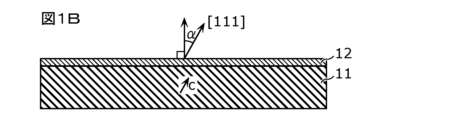
- FIG. 1B is a schematic vertical cross-sectional view illustrating a conductive film forming step in the first embodiment.
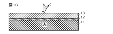
- FIG. 1C is a schematic vertical cross-sectional view showing a piezoelectric film forming step in the first embodiment.
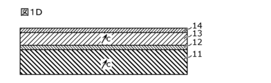
- FIG. 1D is a schematic vertical cross-sectional view illustrating a conductive film forming step in the first embodiment.
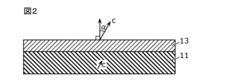
- FIG. 2 is a schematic vertical cross-sectional view showing a piezoelectric film forming step in a modified example of the first embodiment.
- FIG. 1A is a schematic vertical cross-sectional view showing a substrate preparation step in one embodiment of a piezoelectric film production method according to the present invention.
- FIG. 1B is a schematic vertical cross-sectional view illustrating a conductive film forming step in the first embodiment.
- FIG. 1C is a schematic vertical cross-
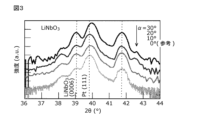
- FIG. 3 is a graph showing the results of X-ray diffraction measurement by 2 ⁇ - ⁇ scanning for the piezoelectric film made of lithium niobate produced by the method of the first embodiment and a reference example.
- FIG. 4 is a graph showing the results of X-ray diffraction measurement by ⁇ scan (fixed 2 ⁇ ) for the piezoelectric film made of lithium niobate produced by the method of the first embodiment and a reference example.
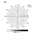
- FIG. 5A is a (10-12) plane pole figure obtained by X-ray diffraction for a piezoelectric film made of lithium niobate with a tilt angle ⁇ of 10°, produced by the method of embodiment 1.
- FIG. 1 is a (10-12) plane pole figure obtained by X-ray diffraction for a piezoelectric film made of lithium niobate with a tilt angle ⁇ of 10°, produced by the method of embodiment 1.
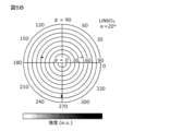
- FIG. 5B is a pole figure of the (10-12) plane obtained by X-ray diffraction for a piezoelectric film made of lithium niobate and having a tilt angle ⁇ of 20°, which was produced by the method of the first embodiment.
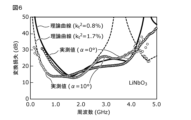
- FIG. 6 is a graph showing measured values and theoretical curves of conversion loss for thin-film resonators obtained using a piezoelectric film made of lithium niobate with a tilt angle ⁇ of 10°, produced by the method of embodiment 1, and a piezoelectric film of a reference example.
- FIG. 10-12 10-12
- FIG. 6 is a graph showing measured values and theoretical curves of conversion loss for thin-film resonators obtained using a piezoelectric film made of lithium niobate with a tilt angle ⁇ of 10°, produced by the method of embodiment 1, and a piezoelectric film of a reference example.
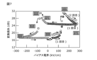
- FIG. 7 is a hysteresis curve showing the results of measuring the minimum conversion loss of a piezoelectric film made of lithium niobate and having an inclination angle ⁇ of 20°, produced by the method of embodiment 1, while changing the strength of the applied DC electric field.
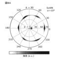
- FIG. 8A is a (10-11) plane pole figure obtained by X-ray diffraction for a piezoelectric film made of scandium aluminum nitride with a tilt angle ⁇ of 10°, produced by the method of embodiment 1.
- FIG. 8B is a pole figure of the (10-11) plane obtained by X-ray diffraction for a magnesium zinc oxide piezoelectric film having an inclination angle ⁇ of 20°, which was produced by the method of embodiment 1.
- FIG. 8A is a (10-11) plane pole figure obtained by X-ray diffraction for a piezoelectric film made of scandium aluminum nitride with a tilt angle ⁇ of 10°, produced by the method of embodiment 1.
- FIG. 9A is a transmission electron microscope photograph of a magnesium zinc oxide piezoelectric film having an inclination angle ⁇ of 20°, which was produced by the method of embodiment 1.
- FIG. 9B is an electron diffraction image obtained on a magnesium zinc oxide piezoelectric film having a tilt angle ⁇ of 20°, which was produced by the method of embodiment 1.
- FIG. 10A is a graph showing measured values and a theoretical curve of the conversion loss for a thin-film resonator obtained using a scandium aluminum nitride piezoelectric film having an inclination angle ⁇ of 10°, which was produced by the method of the first embodiment.
- FIG. 10B is a graph showing measured values and a theoretical curve of the conversion loss for a thin-film resonator obtained using a magnesium zinc oxide piezoelectric film having an inclination angle ⁇ of 20°, which was produced by the method of embodiment 1.
- FIG. 11 is a graph showing the results of X-ray diffraction measurement by 2 ⁇ - ⁇ scanning on a piezoelectric film made of lanthanum-added strontium titanate having an inclination angle ⁇ of 25°, which was produced by the method of embodiment 1.
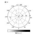
- FIG. 12 is a pole figure of the (101) plane obtained by X-ray diffraction for a piezoelectric film made of lanthanum-added strontium titanate with an inclination angle ⁇ of 25°, which was produced by the method of the first embodiment.
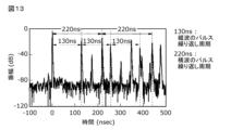
- FIG. 13 is a graph showing the impulse response of a thin-film resonator obtained by using a piezoelectric film made of lanthanum-doped strontium titanate with an inclination angle ⁇ of 25°, which was produced by the method of the first embodiment.
- FIG. 13 is a graph showing the impulse response of a thin-film resonator obtained by using a piezoelectric film made of lanthanum-doped strontium titanate with an inclination angle ⁇ of 25°, which was produced by the method of the first embodiment.
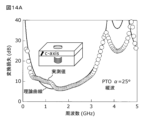
- FIG. 14A is a graph showing measured values and a theoretical curve of the conversion loss of a longitudinal wave for a thin-film resonator obtained using a piezoelectric film made of lanthanum-doped strontium titanate having an inclination angle ⁇ of 25°, which was produced by the method of embodiment 1.
- FIG. 14B is a graph showing measured values and a theoretical curve of the conversion loss of a shear wave for a thin-film resonator obtained using a piezoelectric film made of lanthanum-doped strontium titanate with an inclination angle ⁇ of 25°, which was produced by the method of embodiment 1.
- FIG. 15 is a cross-sectional view of the piezoelectric device according to the second embodiment.
- FIG. 15 is a cross-sectional view of the piezoelectric device according to the second embodiment.
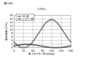
- FIG. 16A is a graph showing the relationship between the second Euler angle and the coupling coefficient when the piezoelectric film is made of lithium tantalate in the piezoelectric device according to the second embodiment.
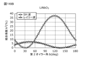
- FIG. 16B is a graph showing the relationship between the second Euler angle and the coupling coefficient when the piezoelectric film is made of lithium niobate in the piezoelectric device according to the second embodiment.
- FIG. 16C is a graph showing the relationship between the second Euler angles and the SH wave/Rayleigh wave ratio of the piezoelectric device according to embodiment 2.
- FIG. 17 is a cross-sectional view of a piezoelectric device according to a modified example of the second embodiment.
- a piezoelectric film made of lithium niobate and having a c-axis, which is a specific crystal axis of orientation, tilted with respect to a direction perpendicular to the film will be described.
- a sapphire substrate 11 is prepared. Sapphire crystals are hexagonal and have six-fold rotational symmetry around the c-axis. The c-axis of this sapphire is the specific crystal axis of the substrate.
- the substrate 11 is fabricated by cutting a single crystal of sapphire so that the tilt direction of the c-axis of the sapphire, which is an insulator, coincides with the tilt direction of the c-axis of the piezoelectric film to be fabricated on the substrate 11 (FIG. 1A: substrate preparation process).
- the single crystal of sapphire can be cut by a cutting device using a laser beam or a diamond wire saw. Since the substrate 11 is sufficiently thicker than the piezoelectric film 13 to be fabricated, the operation of cutting the single crystal of sapphire to fabricate the substrate 11 is easier than the operation of cutting the single crystal of the piezoelectric body into a film (plate).
- a substrate made of silicon carbide or the like having a crystal structure with six-fold rotational symmetry around the c-axis may be used.
- the angle that the substrate specific crystal axis makes with respect to the normal to the surface of the substrate 11 is defined as ⁇ .
- the angle ⁇ is determined so that the inclination direction of the substrate specific crystal axis of the piezoelectric film to be fabricated is aligned with the inclination direction of the orientation specific crystal axis.
- the angle ⁇ is determined within a range of more than 0° and less than 90° so that the inclination direction of the orientation specific crystal axis corresponds to the piezoelectric characteristics required for the piezoelectric film to be fabricated.
- the piezoelectricity in the direction perpendicular to the film can be made higher than when the c-axis is perpendicular to the film, so it is preferable to set the angle ⁇ within the range of 10° to 30°.
- the angle ⁇ may be set to an angle outside the range of 10° to 30°.
- a conductive film 12 is formed by epitaxially growing a film made of platinum on the surface of the substrate 11 (FIG. 1B: conductive film formation process).
- Platinum crystals have a face-centered cubic lattice structure and have six-fold rotational symmetry with respect to the axis in the [111] direction.
- the platinum crystal grows so that the [111] direction of platinum is aligned with the c-axis direction of the sapphire of the substrate 11, and a conductive film 12 made of platinum is formed, which is made of a single crystal facing in the same direction ( ⁇ direction) or a polycrystal oriented in the same direction.
- a metal having a face-centered cubic lattice crystal structure such as gold, aluminum, copper, silver, iridium, etc., may be used as the material for the conductive film 12.
- a film made of lithium niobate is epitaxially grown on the surface of the conductive film 12 to form the piezoelectric film 13 (Fig. 1C: piezoelectric film formation process).
- Lithium niobate crystals are trigonal and have three-fold and six-fold rotational symmetry about the c-axis.
- the lithium niobate is epitaxially grown on the surface of the conductive film 12 made of platinum, which has been crystal-grown so that the [111] direction is aligned with the c-axis direction of the sapphire substrate 11, the lithium niobate grows so that its c-axis is aligned with the c-axis of sapphire and the [111] direction of platinum.
- a piezoelectric film 13 is obtained in which the c-axis of lithium niobate is inclined at an angle ⁇ with respect to the direction perpendicular to the film.
- the conductive film 12 is one of a pair of electrodes used to apply a voltage to the piezoelectric film 13 in the thickness direction, or to detect a voltage generated in the thickness direction of the piezoelectric film 13 by polarization.
- a second conductive film 14 made of a conductor that serves as the other electrode is formed on top of the piezoelectric film 13 (the side opposite the substrate 11) ( Figure 1D: second conductive film formation process).
- the second conductive film 14 does not need to be epitaxially grown, and may be formed by a normal deposition method, etc.
- a film made of lithium niobate may be epitaxially grown directly on the surface of the substrate 11 ( Figure 2).
- the c-axis of the lithium niobate will be in the same direction as the c-axis of the substrate 11, resulting in a piezoelectric film 13 whose c-axis is inclined at an angle ⁇ with respect to the direction perpendicular to the film.
- the conductive film 12 and the piezoelectric film 13 can be produced by the epitaxial method, for example, using a magnetron sputtering device, by appropriately setting the input power, film formation temperature, etc. to adjust the film formation speed. Specific examples of power, film formation temperature, etc. will be described later.
- the piezoelectric film 13 is made of lithium niobate, but the same method can be used to fabricate a piezoelectric film made of other piezoelectric materials.
- a piezoelectric film made of a piezoelectric material having a hexagonal crystal structure such as aluminum nitride (AlN), scandium aluminum nitride (ScAlN), zinc oxide (ZnO), or magnesium zinc oxide (MgZnO)
- a substrate made of sapphire or silicon carbide having six-fold rotational symmetry around the c-axis can be used as in the above embodiment.
- a piezoelectric film made of a piezoelectric material having a crystal structure with four-fold rotational symmetry around the c-axis such as lead titanate (PbTiO 3 )
- a substrate made of strontium titanate (SrTiO 3 ) having four-fold rotational symmetry around the c-axis can be used.
- (2-1) Lithium niobate Three types of piezoelectric films 13 were produced for lithium niobate, with the target values of the inclination angle ⁇ of the c-axis (specific crystal axis for orientation) relative to the film being 10°, 20°, and 30°, respectively.
- the substrate 11 was made of a single crystal of sapphire, and was produced by cutting out the single crystal so that the c-axis (specific crystal axis for the substrate) of the sapphire was inclined at 10°, 20°, and 30°, respectively, from the normal line of the surface of the substrate 11.
- a conductive film 12 made of platinum was formed on the substrate 11, and then a piezoelectric film 13 was formed on the conductive film 12.
- An RF (radio frequency) magnetron sputtering device was used to form the conductive film 12 and the piezoelectric film 13.
- the film formation conditions were as follows.
- Platinum conductive film 12 A platinum target was placed on the cathode of an RF magnetron sputtering device, and a film was formed to a thickness of 50 nm at a temperature of 680° C. in an argon gas atmosphere at a pressure of 0.5 Pa while applying a high frequency power of 80 W.
- Lithium niobate piezoelectric film 13 A target consisting of a powder mixture of a powder of lithium and a powder of niobium in an atomic ratio of 65:35 was placed on the cathode, and a film was formed at a temperature of 650° C. while applying a high frequency power of 100 W in a mixed gas atmosphere of a pressure of 0.5 Pa.
- the mixed gas was a mixture of argon gas and oxygen gas in a partial pressure ratio of 15:1.
- a reference example piezoelectric film made of lithium niobate with a target value of the tilt angle ⁇ of 0° was formed to a thickness of 900 nm under the same conditions as the above three examples, using a substrate in which the c-axis of sapphire was oriented in the normal direction of the surface.
- the abundance ratio of lithium to niobium in the target is set higher than that in lithium niobate (1/1).
- X-ray diffraction measurements were performed on the three piezoelectric films 13 of this embodiment and the piezoelectric film of the reference example.
- the angle of incidence of the X-rays incident on the surface of the piezoelectric film was set to ⁇
- the angle between the incident X-rays and the outgoing X-rays detected by the detector was set to 2 ⁇ .
- the results are shown in FIG. 3.
- the 2 ⁇ - ⁇ scan data for these four piezoelectric films is shifted in the vertical axis direction so as to avoid overlapping as much as possible.
- ⁇ scan was performed by fixing 2 ⁇ at 39.1° and varying only ⁇ .
- the fact that a peak was obtained in the ⁇ scan indicates that the piezoelectric film 13 is a single crystal or a polycrystal with the (0001) plane oriented in the same direction (note that in the case of a non-oriented polycrystal with the (0001) plane not oriented in the same direction, X-rays are detected in the ⁇ scan regardless of the value of ⁇ ).
- the piezoelectric film 13 obtained by the method of this embodiment has good crystallinity equal to or better than that of a piezoelectric film obtained using a substrate with no inclination of the substrate's specific crystal axis.
- pole figures for the (10-12) plane were obtained by X-ray diffraction.
- the obtained pole figures are shown in Figure 5A for the piezoelectric film 13 with a target tilt angle ⁇ of 10° and in Figure 5B for the piezoelectric film 13 with a target tilt angle ⁇ of 20°.
- Figure 5B three poles are seen that show three-fold rotational symmetry around a point where the deflection angle ⁇ is near 20°.
- Figure 5A six poles are seen that show six-fold rotational symmetry around a point where the deflection angle ⁇ is near 10°.
- a thin-film resonator was fabricated by providing a second conductive film 14 on the piezoelectric film 13, and the conversion loss was measured by a network analyzer.
- the measurement result is shown in FIG. 6.
- the DC bias electric field was applied in the range of -280 to +280 kV/cm.
- a positive value of the DC bias electric field means an electric field in which the conductive film 12 side is positive
- a negative value of the DC bias electric field means an electric field in which the conductive film 12 side is negative.
- the DC bias electric field was changed from 0 kV/cm to +280 kV/cm, then from +280 kV/cm to -280 kV/cm, and further from -280 kV/cm to +280 kV/cm. Therefore, measurements were performed twice in the range from 0 kV/cm to +280 kV/cm.
- Figure 7 further shows that the conversion loss hardly changes from the state in which more than half of the polarization is reversed by applying a DC bias electric field of +280 kV/cm, which is higher than the coercive electric field, to the state in which the DC bias electric field is reduced to 0, indicating that the polarization state before the DC bias electric field is reduced is almost maintained.
- the application of the DC bias electric field is stopped (set to 0) when half of the polarization is inverted, the polarization state is thought to be maintained.
- Scandium aluminum nitride, magnesium zinc oxide both have a wurtzite crystal structure and have six-fold rotational symmetry around the c-axis.
- any piezoelectric film made of these materials can generate a thickness-shear mode vibration that vibrates parallel to the film.
- a piezoelectric film made of scandium aluminum nitride and magnesium zinc oxide was fabricated with the c-axis as the specific crystal axis for orientation and the c-axis inclined with respect to the direction perpendicular to the film.
- the substrate 11 was made of single crystal sapphire, and two types were prepared with target values of inclination angle ⁇ of 10° and 20° (the c-axis of sapphire, which is the substrate's specific crystal axis, was inclined 10° and 20° with respect to the normal to the substrate surface).
- An RF magnetron sputtering device was used to form these conductive films 12 and the two types of piezoelectric films 13.
- the film formation conditions are as follows.
- Platinum conductive film 12 A platinum target was placed on the cathode of an RF magnetron sputtering device, and a film was formed to a thickness of 50 nm at a temperature of 700° C. in an argon gas atmosphere at a pressure of 0.5 Pa while applying a high frequency power of 100 W.
- a target made of a plate made of a single aluminum material with particles of simple scandium embedded therein was placed on the cathode so that the atomic ratio of scandium to aluminum was 8:92, and a film was formed to a thickness of 4,500 nm at a temperature of 450° C. while applying a high frequency power of 100 W in a mixed gas atmosphere at a pressure of 0.6 Pa.
- the mixed gas was a mixture of argon gas and nitrogen gas at a partial pressure ratio of 1:3.
- the atomic ratio of scandium to aluminum in the obtained piezoelectric film 13 was confirmed to be 8:92.
- Magnetic zinc oxide piezoelectric film 13 A target made of a mixed powder of magnesium oxide powder and zinc oxide powder so that the atomic ratio of magnesium to zinc was 30:70 was placed on the cathode, and a film was formed to a thickness of 6600 nm at a temperature of 350° C. while applying a high frequency power of 150 W in a mixed gas atmosphere at a pressure of 1.0 Pa.
- the mixed gas was a mixture of argon gas and nitrogen gas at a partial pressure ratio of 20:1.
- Pole figures for the (10-11) plane were obtained by X-ray diffraction for each of the two types of piezoelectric films 13 that were fabricated.
- Six poles exhibiting six-fold rotational symmetry can be seen, with the deflection angle ⁇ at the center near 10° in Figure 8A and the deflection angle ⁇ at the center near 20° in Figure 8B. This indicates that both of these two types of piezoelectric films 13 are oriented so that they are tilted at the target tilt angle with respect to the c-axis direction.
- TEM transmission electron microscope
- the fact that the piezoelectric film 13 has dislocations indicates that the piezoelectric film 13 was produced by the epitaxial method, and that the piezoelectric film 13 has grown epitaxially so that the orientation specific crystal axis, which is the specified crystal axis (c-axis), is inclined from the direction perpendicular to the piezoelectric film 13.
- dislocations refer to linear crystal defects contained in the crystal.
- the presence of dislocations in the piezoelectric film 13 suppresses the occurrence of cracks that tend to occur in single crystals, and prevents the film from peeling off from the substrate 11. This improves the manufacturing yield of the piezoelectric film 13.
- Dislocations in the piezoelectric film can be confirmed by a TEM image such as that shown in Figure 9A.
- the location where a dislocation is confirmed can be confirmed as, for example, a location where the atomic arrangement (a straight chain line connecting the upper left to the lower right in Figure 9A) branches from one row to two rows (dislocation line).
- the dislocation lines exist in the cross-sectional direction (parallel to the surface of the piezoelectric film) as shown in the figure, they can be confirmed by the TEM image as described above.
- the dislocations can be detected by the etch pit method.
- the etch pit method is a method in which the target film is immersed in a corrosive liquid such as an acid or alkaline solution, and the location that is preferentially corroded compared to the surrounding area and causes a depression can be identified as the dislocation location.
- the piezoelectric film 13 may also have a screw dislocation or a threading dislocation.
- a screw dislocation refers to a structure in which the dislocation line and the Burgers vector are parallel and the crystal plane is shifted parallel to the dislocation line.
- a threading dislocation refers to a structure in which the dislocation line penetrates the c-plane.
- a thin-film resonator was fabricated by providing a second conductive film 14 on each of the two types of piezoelectric films 13 fabricated, and the conversion loss of the transverse wave due to thickness-shear vibration was measured by a network analyzer.
- the measurement results are shown in FIG. 10A for the scandium aluminum nitride piezoelectric film 13 and in FIG. 10B for the magnesium zinc oxide piezoelectric film 13.
- the electromechanical coupling coefficient k35 2 related to the thickness-shear vibration is estimated to be 0.72% for the scandium aluminum nitride piezoelectric film 13 and 2.2% for the magnesium zinc oxide piezoelectric film 13.
- the actual measurement value of the conversion loss includes losses due to factors other than the actual conversion loss, the actual electromechanical coupling coefficient k35 2 is considered to be higher than the value estimated here.
- PTO Lead titanate
- the piezoelectric film made of PTO only vibrates in the thickness direction, but when the c-axis is inclined from the direction perpendicular to the film, it can generate thickness-shear vibration.
- a piezoelectric film made of PTO was fabricated in which the c-axis is the orientation specific crystal axis and the c-axis is inclined with respect to the direction perpendicular to the film.
- the target value of the inclination angle ⁇ was set to 25° (the c-axis, which is the substrate specific crystal axis, is inclined 25° with respect to the normal line of the substrate surface).
- the substrate 11 was made by using a substrate made of a single crystal of strontium titanate (STO) having a perovskite crystal structure doped with lanthanum, and cutting out the single crystal so that the c-axis (substrate specific crystal axis) was inclined at 25° from the normal to the surface of the substrate 11. Since the substrate 11 itself is conductive due to being doped with lanthanum in this way, in this example, the piezoelectric film 13 was formed directly on the substrate 11 without providing a conductive film 12. An RF magnetron sputtering device was used to form the piezoelectric film 13. The film formation conditions are as follows:
- piezoelectric film 13 made of PTO A target made of a mixed powder of PTO powder and lead oxide (PbO) powder mixed at a lead atomic ratio of 10:1 (10% excess lead atoms) was placed on the cathode, and a film was formed to a thickness of 0.9 ⁇ m at a temperature of 600° C. while applying a high frequency power of 100 W in a mixed gas atmosphere at a pressure of 0.4 Pa.
- the mixed gas was a mixture of argon gas and oxygen gas at a partial pressure ratio of 25:1.
- X-ray diffraction measurements were performed on the piezoelectric film 13 thus fabricated.
- a 2 ⁇ - ⁇ scan was performed using the usual measurement method in which the angle of incidence of X-rays on the surface of the piezoelectric film 13 is ⁇ .
- a diffraction peak for the (111) plane of PTO can be seen, but no diffraction peaks for the (001) or (002) planes can be seen.
- the piezoelectric film 13 was tilted so that the angle of incidence of the X-rays on the surface of the piezoelectric film 13 was ⁇ +25°, and then a 2 ⁇ - ⁇ scan was performed.
- diffraction peaks of the (001) and (002) planes of the PTO are visible (as well as diffraction peaks of the (001) and (002) planes of the crystal of the substrate 11).
- a pole figure for the (101) plane was obtained by X-ray diffraction for the fabricated piezoelectric film 13.
- the obtained pole figure is shown in Figure 12.
- Four poles showing four-fold rotational symmetry are seen with the deflection angle ⁇ at approximately 25° as the center (one of the poles is slightly weaker, and is therefore indicated by an arrow in the figure).
- a thin-film resonator was fabricated by providing a second conductive film 14 on the piezoelectric film 13 thus fabricated.
- the reflection coefficient S11 of the thin-film resonator was measured using a network analyzer, and an inverse Fourier transform was then performed to calculate the impulse response in the time domain.
- This impulse response shows a repeating pulse-like response over time, as a result of ultrasonic waves generated in a pulsed form at a certain time being multiple-reflected on both the front and back sides of the piezoelectric film of the thin-film resonator.
- the calculated impulse response is shown in Figure 13.
- This impulse response shows peaks that repeat every 130 nsec (nanoseconds) and peaks that repeat every 220 nsec.
- the former is thought to be due to longitudinal waves caused by vibrations perpendicular to the film, and the latter is thought to be due to transverse waves caused by thickness-shear vibrations.
- the conversion loss of the longitudinal wave and the transverse wave of the fabricated thin film resonator was measured by a network analyzer.
- the measurement results are shown in Fig. 14A for the longitudinal wave and in Fig. 14B for the transverse wave.
- the electromechanical coupling coefficient k332 for the vibration perpendicular to the film is estimated to be 13.5%
- the electromechanical coupling coefficient k352 for the thickness shear vibration is estimated to be 17.9%.
- the piezoelectric film 13 may be a piezoelectric film made of lithium tantalate.
- the piezoelectric film 13 grows epitaxially so that the specific crystal axis (c-axis), which is a predetermined crystal axis, is inclined from the direction perpendicular to the piezoelectric film 13.
- the piezoelectric film 13 By making the piezoelectric film 13 from lithium niobate or lithium tantalate, a large electromechanical coupling coefficient can be obtained, and good frequency-temperature characteristics can also be obtained.
- the piezoelectric film 13 according to this embodiment may be doped with impurities, since it is formed using a sputtering method or the like. Impurities may be doped into the piezoelectric film 13 in two ways: by actively adding (doping) the impurities, and by unintentionally including the impurities.
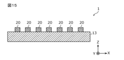
- FIG 15 is a cross-sectional view of a Lamb wave device 1 according to embodiment 2.
- the Lamb wave device 1 is an example of a piezoelectric device, and utilizes Lamb waves (a type of plate wave) that propagate through a piezoelectric film 13 (in the X-axis direction in Figure 15).
- the Lamb wave device 1 includes a piezoelectric film 13 and an IDT (InterDigital Transducer) electrode 20.
- IDT InterDigital Transducer
- the piezoelectric film 13 is the piezoelectric film 13 according to the first embodiment, and is a piezoelectric film that has been epitaxially grown such that the specific crystal axis (c-axis), which is a predetermined crystal axis, is inclined from the direction perpendicular to the piezoelectric film 13 (Z-axis in FIG. 15) around the X-axis (at the second Euler angle b° toward the Y-axis in FIG. 15).
- the piezoelectric film 13 is made of, for example, lithium tantalate or lithium niobate.
- the relationship between the principal surface of the piezoelectric film 13 and the Euler angles (first Euler angle, second Euler angle, third Euler angle) expressing the propagation direction of the Lamb wave will be described.
- the CX axis is rotated counterclockwise around the CZ axis by the first Euler angle with respect to the crystal axis (CX, CY, CZ (c-axis)) of the piezoelectric film 13 to obtain the Xa axis.
- the CZ axis is rotated counterclockwise around the Xa axis by the second Euler angle to obtain the Z' axis.
- the surface including the Xa axis and having the Z' axis as its normal line becomes the principal surface of the piezoelectric film 13.
- the X' axis direction obtained by rotating the Xa axis counterclockwise around the Z' axis by the third Euler angle becomes the propagation direction of the Lamb wave.
- the X axis in FIG. 15 corresponds to the X' axis in the above explanation of the Euler angles
- the Z axis in FIG. 15 corresponds to the Z' axis in the above explanation of the Euler angles.
- the IDT electrode 20 is composed of a pair of comb-shaped electrodes facing each other.
- Each of the pair of comb-shaped electrodes is composed of a number of parallel electrode fingers and a busbar electrode that connects the multiple electrode fingers.
- the multiple electrode fingers are formed along a direction (Y-axis direction) perpendicular to the elastic wave propagation direction (X-axis direction).
- the electromechanical coupling coefficient k2 was calculated when the first and third Euler angles (first Euler angle, second Euler angle b, third Euler angle) were set to 0° and the second Euler angle b was changed.
- the electrode duty of the IDT electrode 20 was set to 0.5
- the wavelength ⁇ tilt the pitch of adjacent electrode fingers
- the film thickness of the IDT electrode 20 was set to 0.05 ⁇
- the film thickness of the piezoelectric film 13 was set to 0.15 ⁇ .
- Fig. 16A is a graph showing the relationship between the second Euler angle b and the electromechanical coupling coefficient k2 when the piezoelectric film 13 is lithium tantalate in the Lamb wave device 1 according to embodiment 2.
- Fig. 16B is a graph showing the relationship between the second Euler angle b and the electromechanical coupling coefficient k2 when the piezoelectric film 13 is lithium niobate in the piezoelectric device 1 according to embodiment 2.
- Fig. 16C is a graph showing the relationship between the second Euler angle b and the SH wave/Rayleigh wave ratio in the piezoelectric device 1 according to embodiment 2.
- the electromechanical coupling coefficient k2 of the SH wave is larger than that of the Rayleigh wave when the second Euler angle b is in the range of 0° to 10° and 55° to 180°. This makes it possible to use the SH wave as the main mode when the piezoelectric film 13 is made of lithium tantalate.
- the second Euler angle b is desirably equal to or greater than 100° and equal to or less than 160°, as shown in Fig. 16C.
- the electromechanical coupling coefficient k2 of the SH wave can be made 20 times or more larger than the electromechanical coupling coefficient k2 of the Rayleigh wave.
- the piezoelectric film 13 of the piezoelectric device 1 is lithium tantalate
- the second Euler angle b is 125° or more and 140° or less, as shown in Fig. 16C.
- the electromechanical coupling coefficient k2 of the SH wave can be made 200 times or more larger than the electromechanical coupling coefficient k2 of the Rayleigh wave.
- the electromechanical coupling coefficient k2 of the SH wave is larger than that of the Rayleigh wave when the second Euler angle b is in the range of 0° to 5° and in the range of 60° to 180°. This means that when the piezoelectric film 13 is made of lithium niobate, it is possible to use the SH wave as the main mode.
- the second Euler angle b is desirably 110° or more and 155° or less, as shown in Fig. 16C. According to this, when the piezoelectric film 13 is made of lithium niobate, the electromechanical coupling coefficient k2 of the SH wave can be made 20 times or more larger than the electromechanical coupling coefficient k2 of the Rayleigh wave.
- the piezoelectric film 13 of the piezoelectric device 1 is made of lithium niobate
- the second Euler angle b is equal to or greater than 130° and equal to or less than 140°, as shown in Fig. 16C.
- the electromechanical coupling coefficient k2 of the SH wave can be made 200 times or more larger than the electromechanical coupling coefficient k2 of the Rayleigh wave.
- the first Euler angle and the third Euler angle are set to 0°, but the first Euler angle and the third Euler angle do not have to be strictly 0°, and if they are 0° ⁇ 10°, they will have substantially the same effect.
- FIG. 17 is a cross-sectional view of a piezoelectric device 2 according to a modified example of embodiment 2.
- the piezoelectric device 2 includes a piezoelectric film 13, a substrate 11, a low acoustic velocity layer 33, a high acoustic velocity layer 32, a support substrate 31, and an IDT electrode 20.
- the piezoelectric film 13 is the piezoelectric film 13 according to the first embodiment, and is a piezoelectric film that has been epitaxially grown such that the specific crystal axis (c-axis), which is a predetermined crystal axis, is inclined from the direction perpendicular to the piezoelectric film 13 (Z-axis) around the X-axis (by the second Euler angle b° in the Y-axis direction).
- the piezoelectric film 13 is made of, for example, lithium tantalate or lithium niobate.
- the substrate 11 is the substrate 11 according to the first embodiment, and is an insulating layer made of a single crystal or polycrystalline insulator that is in contact with the piezoelectric film 13 and has the same rotational symmetry with respect to a specific crystal axis (c-axis) that is a specific crystal axis, and that has the same inclination as the inclination of the specific crystal axis.
- c-axis specific crystal axis
- the substrate 11 is made of an insulating material such as sapphire, silicon carbide, lithium tantalate, or lithium niobate.
- the insulating layer of the substrate 11 is in contact with the piezoelectric film 13, which can improve and optimize the elasticity, dielectric properties, and their temperature dependences of the piezoelectric film 13.
- the substrate 11 is made of a piezoelectric material such as lithium tantalate or lithium niobate, the piezoelectricity and its temperature dependence of the piezoelectric film 13 can be improved and optimized.
- the substrate 11 may be a semiconductor layer made of a single crystal or polycrystalline semiconductor that is in contact with the piezoelectric film 13 and has the same rotational symmetry with respect to a specific crystal axis (c-axis) that is a specific crystal axis, and that has the same inclination as the specific crystal axis.
- the semiconductor material is, for example, silicon.
- the support substrate 31 is a substrate that supports the high acoustic velocity layer 32, the low acoustic velocity layer 33, the substrate 11, the piezoelectric film 13, and the IDT electrode 20.
- the material of the support substrate 31 may be, for example, a piezoelectric material such as aluminum nitride, lithium tantalate, lithium niobate, or quartz; a ceramic material such as alumina, sapphire, magnesia, silicon nitride, silicon carbide, zirconia, cordierite, mullite, steatite, or forsterite; a dielectric material such as diamond or glass; a semiconductor material such as silicon or gallium nitride; or a resin; or a material containing the above materials as a main component.
- a piezoelectric material such as aluminum nitride, lithium tantalate, lithium niobate, or quartz
- a ceramic material such as alumina, sapphire, magnesia, silicon nitride, silicon carbide, zirconia, cordierite, mullite, steatite, or forsterite
- a dielectric material such as diamond or glass
- a semiconductor material such as
- the low acoustic velocity layer 33 is disposed between the substrate 11 and the support substrate 31, and is a layer in which the acoustic velocity of the bulk waves is slower than that of the bulk waves propagating through the piezoelectric film 13. Due to the property of elastic waves that energy is concentrated in a medium with an essentially low acoustic velocity, leakage of surface acoustic wave energy outside the piezoelectric film 13 is suppressed.
- the low sound velocity layer 33 can be made of a dielectric material such as glass, silicon oxide, silicon oxynitride, lithium oxide, tantalum oxide, or a compound of silicon oxide with fluorine, carbon, or boron, or a material that contains the above materials as its main component.
- a dielectric material such as glass, silicon oxide, silicon oxynitride, lithium oxide, tantalum oxide, or a compound of silicon oxide with fluorine, carbon, or boron, or a material that contains the above materials as its main component.
- the high acoustic velocity layer 32 is disposed between the low acoustic velocity layer 33 and the support substrate 31, and is a layer in which the acoustic velocity of the bulk waves propagating therethrough is faster than the acoustic velocity of the elastic waves propagating through the piezoelectric film 13.
- the material of the high sound velocity layer 32 may be, for example, a piezoelectric material such as aluminum nitride, lithium tantalate, lithium niobate, or quartz, a ceramic material such as alumina, sapphire, magnesia, silicon nitride, silicon carbide, zirconia, cordierite, mullite, steatite, forsterite, spinel, or sialon, a dielectric material such as aluminum oxide, silicon oxynitride, DLC (diamond-like carbon), or diamond, or a semiconductor material such as silicon, or a material mainly composed of the above-mentioned material.
- a piezoelectric material such as aluminum nitride, lithium tantalate, lithium niobate, or quartz
- a ceramic material such as alumina, sapphire, magnesia, silicon nitride, silicon carbide, zirconia, cordierite, mullite, steatite, forsterite,
- the spinel includes an aluminum compound containing one or more elements selected from Mg, Fe, Zn, Mn, and the like, and oxygen.
- Examples of the spinel include MgAl 2 O 4 , FeAl 2 O 4 , ZnAl 2 O 4 , and MnAl 2 O 4 .
- the piezoelectric device 2 only needs to include the piezoelectric film 13, the substrate 11, and the IDT electrode 20, and does not need to include at least one of the low acoustic velocity layer 33, the high acoustic velocity layer 32, and the support substrate 31.
- the piezoelectric device 2 may also include a piezoelectric film 13, a substrate 11, an IDT electrode 20, a support substrate 31, and an energy trapping layer.
- the piezoelectric device 2 has a structure in which the support substrate 31, the energy trapping layer, the substrate 11, the piezoelectric film 13, and the IDT electrode 20 are stacked in this order.
- the energy trapping layer is composed of one or more layers, and the speed of the bulk acoustic waves propagating through at least one of the layers is greater than the speed of the acoustic waves propagating near the piezoelectric film 13.
- the energy trapping layer may have a laminated structure of a low acoustic velocity layer and a high acoustic velocity layer.
- the energy trapping layer may also be an acoustic impedance layer having a structure in which low acoustic impedance layers with a relatively low acoustic impedance and high acoustic impedance layers with a relatively high acoustic impedance are alternately laminated.
- the piezoelectric device 2 according to this modified example can improve and optimize the piezoelectricity and temperature dependence of the piezoelectric film 13.
- the rotational symmetry of the substrate 11 and the piezoelectric film 13 can be obtained by the following method.
- XRD pole measurements are used and the diffraction peaks that appear are corrected for the tilt of the axis, a pole figure with rotational symmetry about the center appears.
- the rotational symmetry of the substrate 11 and the piezoelectric film 13 can be obtained.
- an electron beam diffraction pattern corresponding to the symmetry of the crystal structure can be obtained, and by analyzing this diffraction pattern, the rotational symmetry can be measured with high precision.
- the inclination of the orientation-specific crystal axis and the substrate-specific crystal axis can be obtained by the following methods. Using the electron beam diffraction of XRD, TEM, or SEM, for example, in XRD, the inclination can be obtained from the angle corrected to produce a pole figure with rotational symmetry about the center. In addition, in TEM and SEM, a diffraction pattern of the electron beam appears, and the inclination can be obtained by analyzing this diffraction pattern.
- the tilt angles of the orientation specific crystal axis and the substrate specific crystal axis are defined as being the same when the difference between the tilt angles is within the range of ⁇ 16°, regardless of the direction of tilt.
- the difference between the two tilt angles is preferably within the range of ⁇ 5°.
- the piezoelectric film manufacturing method is a method for manufacturing a piezoelectric film made of a single crystal or polycrystalline piezoelectric body in which a specific orientation crystal axis, which is a predetermined crystal axis, is tilted from a direction perpendicular to the film, and includes a substrate preparation step of preparing a substrate made of a single crystal having the same rotational symmetry with respect to a specific substrate crystal axis, which is the predetermined crystal axis, as the rotational symmetry with respect to the specific orientation crystal axis in the piezoelectric body, and the substrate specific crystal axis has the same inclination as the inclination of the specific orientation crystal axis, and a piezoelectric film formation step of forming a piezoelectric film made of the piezoelectric body on the substrate by an epitaxial method.
- the piezoelectric film manufacturing method according to 2 is the piezoelectric film manufacturing method according to 1, which includes, between the substrate preparation step and the piezoelectric film formation step, a conductive film formation step of forming, on the surface of the substrate, a conductive film made of a conductive material having the same rotational symmetry about a specific crystal axis as the rotational symmetry about the specific crystal axis of the substrate, by an epitaxial method.
- the piezoelectric film according to Clause 3 is epitaxially grown so that the specific crystal axis, which is a predetermined crystal axis, is tilted from the direction perpendicular to the film.
- the piezoelectric film according to paragraph 4 has crystal dislocations in the piezoelectric film according to paragraph 3.
- the piezoelectric film according to 5 is the piezoelectric film according to 3 or 4, and is made of lithium niobate or lithium tantalate.
- the piezoelectric film according to 6 is a piezoelectric film according to any one of 3 to 5, which is in contact with a conductive film made of a single crystal or polycrystalline conductor having the same rotational symmetry about a specified crystal axis as the rotational symmetry about the specific crystal axis of orientation, and the specified crystal axis having the same inclination as the inclination of the specific crystal axis of orientation.
- the piezoelectric film according to 7 is a piezoelectric film according to any one of 3 to 6, in which the polarization components perpendicular to the piezoelectric film are oriented in opposite directions between one surface side and the other surface side of the piezoelectric film.
- the piezoelectric device according to 8 has a piezoelectric film according to any one of 3 to 7.
- the piezoelectric device according to item 9 is the piezoelectric device according to item 8, further comprising an insulating layer made of a single crystal or polycrystalline insulator, in contact with the piezoelectric film, having the same rotational symmetry about a specified crystal axis as the rotational symmetry about the specific crystal axis of orientation, and the specified crystal axis having the same inclination as the inclination of the specific crystal axis of orientation.
- the piezoelectric device according to item 10 is the piezoelectric device according to item 8, further comprising a semiconductor layer made of a single crystal or polycrystalline semiconductor, in contact with the piezoelectric film, having the same rotational symmetry about a predetermined crystal axis as the rotational symmetry about the specific crystal axis of orientation, and the predetermined crystal axis having the same inclination as the inclination of the specific crystal axis of orientation.
- the piezoelectric device according to item 11 is the piezoelectric device according to item 9, further comprising a support substrate, a low acoustic velocity layer disposed between the insulating layer and the support substrate, the low acoustic velocity layer having a bulk wave with a slower acoustic velocity than the bulk wave propagating through the piezoelectric film, and a high acoustic velocity layer disposed between the low acoustic velocity layer and the support substrate, the high acoustic velocity layer having a bulk wave with a faster acoustic velocity than the elastic wave propagating through the piezoelectric film.
- the piezoelectric device according to clause 12 is the piezoelectric device according to clause 9 or 11, in which the insulating layer is made of lithium niobate or lithium tantalate.
- the piezoelectric device according to clause 13 is a piezoelectric device according to any one of clauses 8 to 12, and is any one of an SMR type device, an FBAR type device, an XBAR type device, a SAW device, and a Lamb wave device.
- the piezoelectric device according to clause 14 is the piezoelectric device according to clause 8, wherein the piezoelectric device is a Lamb wave device, the piezoelectric film is made of lithium tantalate, and the second Euler angle of the piezoelectric film is 0° or more and 10° or less, or 55° or more and 180° or less.
- the piezoelectric device according to Item 15 is the piezoelectric device according to Item 14, in which the second Euler angle of the piezoelectric film is 100° or more and 160° or less.
- the piezoelectric device according to Item 16 is the piezoelectric device according to Item 14, in which the second Euler angle of the piezoelectric film is 125° or more and 140° or less.
- the piezoelectric device according to clause 17 is the piezoelectric device according to clause 8, wherein the piezoelectric device is a Lamb wave device, the piezoelectric film is made of lithium niobate, and the second Euler angle of the piezoelectric film is 0° or more and 5° or less, or 60° or more and 180° or less.
- the piezoelectric device according to Item 18 is the piezoelectric device according to Item 17, in which the second Euler angle of the piezoelectric film is 110° or more and 155° or less.
- the piezoelectric device according to Item 19 is the piezoelectric device according to Item 17, in which the second Euler angle of the piezoelectric film is 130° or more and 140° or less.
Landscapes
- Chemical & Material Sciences (AREA)
- Engineering & Computer Science (AREA)
- Materials Engineering (AREA)
- Inorganic Chemistry (AREA)
- Organic Chemistry (AREA)
- Metallurgy (AREA)
- Manufacturing & Machinery (AREA)
- Ceramic Engineering (AREA)
- Crystallography & Structural Chemistry (AREA)
- Chemical Kinetics & Catalysis (AREA)
- Mechanical Engineering (AREA)
- Power Engineering (AREA)
- Crystals, And After-Treatments Of Crystals (AREA)
Abstract
Description
本発明は、スマートフォン等の通信機器で使用される周波数フィルタ等に用いられる圧電膜の作製方法に関する。 The present invention relates to a method for producing piezoelectric films used in frequency filters in communication devices such as smartphones.
従来より、特定の周波数帯の電気信号を通過させる周波数フィルタとして、圧電膜の表面に生じる表面弾性波(SAW:Surface Acoustic Wave)を利用するSAWフィルタや、圧電膜のバルクの振動を利用するバルク音響波(BAW:Bulk Acoustic Wave)フィルタといった、圧電膜を備える周波数フィルタが用いられている。これらSAWフィルタやBAWフィルタでは、圧電性を生じさせる方向を揃えるために、特定の一方向に配向した単結晶又は多結晶の圧電膜が用いられている。 Conventionally, frequency filters equipped with piezoelectric films, such as SAW filters that utilize the surface acoustic waves (SAW: Surface Acoustic Wave) generated on the surface of a piezoelectric film, and Bulk Acoustic Wave (BAW: Bulk Acoustic Wave) filters that utilize the bulk vibration of a piezoelectric film, have been used as frequency filters that allow electrical signals of a specific frequency band to pass. These SAW and BAW filters use single-crystal or polycrystalline piezoelectric films oriented in a specific direction to align the direction in which piezoelectricity is generated.
特許文献1には、ニオブ酸リチウム(LiNbO3)の単結晶から成る圧電膜を備えるBAWフィルタが記載されている。ニオブ酸リチウムは、c軸の周りに3回回転対称性を有する三方晶系の結晶構造を有する。ニオブ酸リチウムの膜は、c軸が膜に垂直に配向している場合よりも、膜に垂直な方向から傾斜した方向に配向している場合の方が、膜に垂直な方向に高い圧電性を生じさせることができる。そのため、特許文献1に記載のBAWフィルタでは、ニオブ酸リチウムのバルク単結晶を、c軸が膜に垂直な方向から傾斜した方向となるように板状に切断したものを圧電膜として用いている。
従来より、多くの圧電膜はスパッタ法等を用いることで直接(切断の操作を行うことなく)、膜状となるように作製されている。ニオブ酸リチウムについても、そのような方法を用いてc軸が膜に垂直な方向から傾斜した膜が得られれば、切断の操作が不要になり、作製が容易になる。しかし、スパッタ法を用いてニオブ酸リチウムの膜を作製すると、c軸が膜に垂直な方向を向いてしまい(例えば特許文献2参照)、c軸が膜に垂直な方向から傾斜したニオブ酸リチウムの膜を得ることはできない。 Traditionally, many piezoelectric films have been produced directly (without cutting) into a film shape by using a sputtering method or the like. If such a method could be used to obtain a lithium niobate film whose c-axis is tilted from the direction perpendicular to the film, the cutting operation would be unnecessary and production would be easier. However, when a lithium niobate film is produced using a sputtering method, the c-axis will be oriented in a direction perpendicular to the film (see, for example, Patent Document 2), and it is not possible to obtain a lithium niobate film whose c-axis is tilted from the direction perpendicular to the film.
ここまではニオブ酸リチウムを例として、膜に垂直な方向の圧電性を高くするためにc軸が膜に垂直な方向から傾斜した圧電膜を得る場合の問題を述べた。一方、窒化スカンジウムアルミニウム(ScAlN)や酸化マグネシウム亜鉛(MgZnO)等の圧電体では、膜に平行な方向のすべり振動を生成するために、膜に平行な方向に高い圧電性を生じさせるべく、特定の軸(六方晶のc軸)が膜に垂直な方向から傾斜した圧電膜が用いられている。これらの圧電膜の作製においてもニオブ酸リチウム製の圧電膜と同様の問題が生じる。 So far, we have used lithium niobate as an example to discuss the problems involved in obtaining a piezoelectric film whose c-axis is tilted from the direction perpendicular to the film in order to increase the piezoelectricity in the direction perpendicular to the film. On the other hand, with piezoelectric materials such as scandium aluminum nitride (ScAlN) and magnesium zinc oxide (MgZnO), a piezoelectric film is used in which a specific axis (the c-axis of the hexagonal crystal) is tilted from the direction perpendicular to the film in order to generate shear vibrations parallel to the film and thus generate high piezoelectricity in the direction parallel to the film. The production of these piezoelectric films also presents the same problems as with piezoelectric films made from lithium niobate.
本発明が解決しようとする課題は、バルク単結晶を膜状に切り出す操作を行うことなく、所定の結晶軸が膜に垂直な方向から特定の一方向に傾斜した単結晶又は多結晶の圧電膜を作製する方法を提供することである。 The problem that this invention aims to solve is to provide a method for producing a single crystal or polycrystalline piezoelectric film in which a predetermined crystal axis is tilted in a specific direction from the direction perpendicular to the film, without cutting a bulk single crystal into a film.
上記課題を解決するために成された本発明に係る圧電膜作製方法は、所定の結晶軸である配向特定結晶軸が膜に垂直な方向から傾斜した単結晶又は多結晶の圧電体から成る圧電膜を作製する方法であって、前記圧電体における前記配向特定結晶軸に関する回転対称性と同じ回転対称性を所定の結晶軸である基板特定結晶軸に関して有する単結晶から成る基板であって、該基板特定結晶軸が前記配向特定結晶軸の傾斜と同じ傾斜を有する基板を準備する基板準備工程と、前記基板上にエピタキシャル法により前記圧電体から成る圧電膜を成膜する圧電膜成膜工程とを有する。 The piezoelectric film manufacturing method according to the present invention, which has been developed to solve the above problems, is a method for manufacturing a piezoelectric film made of a single crystal or polycrystalline piezoelectric body in which a specific orientation crystal axis, which is a predetermined crystal axis, is tilted from a direction perpendicular to the film, and includes a substrate preparation step of preparing a substrate made of a single crystal that has the same rotational symmetry with respect to a specific substrate crystal axis, which is the predetermined crystal axis, as the rotational symmetry with respect to the specific orientation crystal axis in the piezoelectric body, and in which the specific substrate crystal axis has the same inclination as the inclination of the specific orientation crystal axis, and a piezoelectric film formation step of forming a piezoelectric film made of the piezoelectric body on the substrate by an epitaxial method.
本発明に係る圧電膜作製方法では、作製しようとする圧電膜の配向特定結晶軸に関する回転対称性と、基板の基板特定結晶軸に関する回転対称性を合わせる。すなわち結晶構造がそのような回転対称性を有する材料から成る基板を用いる。それと共に、作製しようとする圧電膜の配向特定結晶軸と基板の基板特定結晶軸が同じ傾斜を有するように基板特定結晶軸の向きを配向特定結晶軸の向きに合わせた基板を準備する。このような基板上にエピタキシャル法により前記圧電体から成る圧電膜を成膜することにより、圧電膜は基板の単結晶に整合しつつ、配向特定結晶軸が基板特定結晶軸と同じ方向を向くように成長する。これにより、配向特定結晶軸が膜に垂直な方向から特定の一方向に傾斜した単結晶又は多結晶の圧電膜が得られる。 In the piezoelectric film manufacturing method according to the present invention, the rotational symmetry of the orientation-specific crystal axis of the piezoelectric film to be manufactured is matched to the rotational symmetry of the substrate-specific crystal axis of the substrate. In other words, a substrate made of a material whose crystal structure has such rotational symmetry is used. At the same time, a substrate is prepared in which the orientation-specific crystal axis of the substrate is aligned with the orientation-specific crystal axis so that the orientation-specific crystal axis of the piezoelectric film to be manufactured and the substrate-specific crystal axis of the substrate have the same inclination. By forming a piezoelectric film made of the piezoelectric material on such a substrate by the epitaxial method, the piezoelectric film grows so that the orientation-specific crystal axis faces the same direction as the substrate-specific crystal axis while being aligned with the single crystal of the substrate. This results in a single-crystal or polycrystalline piezoelectric film in which the orientation-specific crystal axis is inclined in a specific direction from the direction perpendicular to the film.
配向特定結晶軸に関して3回回転対称性を有する圧電膜を作製する場合には、基板には、基板特定結晶軸に関して3回回転対称性又は6回回転対称性を有する材料から成るもの(6回回転対称性を有するものは、3回回転対称性も満たしている)を用いることができる。配向特定結晶軸に関して6回回転対称性を有する圧電体の膜を作製する場合には、基板には、基板特定結晶軸に関して6回回転対称性を有する材料から成るものを用いる。配向特定結晶軸に関して4回回転対称性を有する圧電体の膜を作製する場合には、基板には、基板特定結晶軸に関して4回回転対称性を有する材料から成るものを用いる。 When making a piezoelectric film that has three-fold rotational symmetry about the specific crystal axis of the orientation, the substrate can be made of a material that has three-fold or six-fold rotational symmetry about the specific crystal axis of the substrate (those that have six-fold rotational symmetry also satisfy three-fold rotational symmetry). When making a piezoelectric film that has six-fold rotational symmetry about the specific crystal axis of the orientation, the substrate can be made of a material that has six-fold rotational symmetry about the specific crystal axis of the substrate. When making a piezoelectric film that has four-fold rotational symmetry about the specific crystal axis of the orientation, the substrate can be made of a material that has four-fold rotational symmetry about the specific crystal axis of the substrate.
例えば、c軸に関して3回回転対称性を有する圧電体であるニオブ酸リチウムの膜を作製する場合には、基板には特定の軸に関して3回回転対称性又は6回回転対称性を有する結晶構造の材料を用いることができる。例えば、c軸に関して3回回転対称性又は6回回転対称性を有する三方晶又は六方晶の結晶構造のサファイヤ(Al2O3)、炭化ケイ素(SiC)、チタン(Ti)、ガリウムリン(GaP)等から成る基板を用いることができる。また、(111)面に垂直な軸に関して3回回転対称性を有する立方晶のチタン酸ストロンチウム(SrTiO3)、酸化マグネシウム(MgO)、アルミニウム(Al)、シリコン(Si)、ゲルマニウム(Ge)、ガリウムヒ素(GaAs)、イットリア安定化ジルコニア(YSZ)等から成り、(111)面を表面とする基板等を用いることができる。c軸に関して6回回転対称性を有する圧電体である窒化スカンジウムアルミニウムや酸化マグネシウム亜鉛の膜を作製する場合にも、これらと同様の基板を用いることができる。 For example, when preparing a film of lithium niobate, which is a piezoelectric material having three-fold rotational symmetry with respect to the c-axis, a material having a crystal structure having three-fold or six-fold rotational symmetry with respect to a specific axis can be used for the substrate. For example, a substrate made of sapphire (Al 2 O 3 ), silicon carbide (SiC), titanium (Ti), gallium phosphide (GaP), etc., having a trigonal or hexagonal crystal structure having three-fold or six-fold rotational symmetry with respect to the c-axis can be used. In addition, a substrate made of cubic strontium titanate (SrTiO 3 ), magnesium oxide (MgO), aluminum (Al), silicon (Si), germanium (Ge), gallium arsenide (GaAs), yttria stabilized zirconia (YSZ), etc., having three-fold rotational symmetry with respect to an axis perpendicular to the (111) plane, and having a (111) plane as a surface, can be used. Substrates similar to these can also be used to fabricate films of scandium aluminum nitride or magnesium zinc oxide, which are piezoelectric materials having six-fold rotational symmetry about the c-axis.
c軸に関して4回回転対称性を有する圧電体であるチタン酸鉛(PTO:PbTiO3)やチタン酸ジルコン酸鉛(PZT:Pb(Zr,Ti)O3)等の膜を作製する場合には、基板にはc軸に関して4回回転対称性を有する結晶構造の材料を用いることができる。例えば、(100)面に垂直な軸に関して4回回転対称性を有する立方晶のチタン酸ストロンチウム、酸化マグネシウム、アルミニウム、シリコン、ゲルマニウム、ガリウムヒ素、イットリア安定化ジルコニア等から成り、(100)面を表面とする基板等を用いることができる。 When producing a film of a piezoelectric material having four-fold rotational symmetry about the c-axis, such as lead titanate (PTO: PbTiO3 ) or lead zirconate titanate (PZT: Pb(Zr,Ti) O3 ), a material having a crystal structure having four-fold rotational symmetry about the c-axis can be used for the substrate. For example, a substrate made of cubic strontium titanate, magnesium oxide, aluminum, silicon, germanium, gallium arsenide, yttria-stabilized zirconia, or the like having four-fold rotational symmetry about an axis perpendicular to the (100) plane, and having a (100) surface, can be used.
本発明に係る圧電膜作製方法において、前記基板準備工程と前記圧電膜成膜工程との間に、前記基板の表面に、前記基板特定結晶軸に関する回転対称性と同じ回転対称性を所定の結晶軸に関して有する導電性の材料から成る導電膜をエピタキシャル法により成膜する導電膜成膜工程を有し、前記圧電膜成膜工程では前記導電膜の表面に前記圧電膜を成膜するという方法を取ることができる。 In the piezoelectric film manufacturing method according to the present invention, between the substrate preparation step and the piezoelectric film deposition step, a conductive film deposition step is provided in which a conductive film made of a conductive material having the same rotational symmetry about a specific crystal axis as the substrate specific crystal axis is deposited on the surface of the substrate by an epitaxial method, and the piezoelectric film is deposited on the surface of the conductive film in the piezoelectric film deposition step.
このような導電膜を介して基板上に圧電膜を成膜する場合にも、配向特定結晶軸が基板特定結晶軸と同じ方向を向いた圧電膜を得ることができる。この場合には導電膜を、圧電膜に印加する電圧の電極の1つとして用いることができる。 When a piezoelectric film is formed on a substrate via such a conductive film, it is possible to obtain a piezoelectric film whose specific crystal axis is oriented in the same direction as the specific crystal axis of the substrate. In this case, the conductive film can be used as one of the electrodes for applying a voltage to the piezoelectric film.
例えば、c軸に関して3回回転対称性又は6回回転対称性を有する圧電体の膜を作製する場合において、サファイヤや炭化ケイ素といったc軸に関して3回回転対称性又は6回回転対称性を有する材料から成る基板を用いる場合には、導電膜の材料には[111]方向の軸に関して3回回転対称性及び6回回転対称性を有する白金を好適に用いることができる。 For example, when making a piezoelectric film having three-fold or six-fold rotational symmetry about the c-axis, if a substrate made of a material having three-fold or six-fold rotational symmetry about the c-axis, such as sapphire or silicon carbide, is used, platinum, which has three-fold or six-fold rotational symmetry about the [111] axis, can be suitably used as the material for the conductive film.
本発明の方法により作製される圧電膜は、所定の結晶軸である配向特定結晶軸が膜に垂直な方向から傾斜するようにエピタキシャル成長しているものであることを特徴とする。このようにエピタキシャル成長している圧電膜の断面を透過電子顕微鏡(TEM)で観察すると、線状の結晶欠陥である転位が存在することが観測される。このような転位は、バルクの圧電体の単結晶ではほとんどみられず、エピタキシャル成長している圧電膜であることの証拠となる。 The piezoelectric film produced by the method of the present invention is characterized by being epitaxially grown so that the specific crystal axis, which is a predetermined crystal axis, is tilted from the direction perpendicular to the film. When a cross section of such an epitaxially grown piezoelectric film is observed with a transmission electron microscope (TEM), the presence of dislocations, which are linear crystal defects, is observed. Such dislocations are rarely seen in bulk piezoelectric single crystals, and are evidence that the piezoelectric film has grown epitaxially.
前記圧電膜はさらに、前記配向特定結晶軸に関する回転対称性と同じ回転対称性を所定の結晶軸に関して有し、該所定の結晶軸が前記配向特定結晶軸の傾斜と同じ傾斜を有する単結晶又は多結晶の導電体から成る導電膜に接している、という構成を取ることができる。このような構成は、本発明の方法において導電膜を介して基板上に圧電膜を成膜することにより得られる。 The piezoelectric film can further be configured to be in contact with a conductive film made of a single crystal or polycrystalline conductor that has the same rotational symmetry about a specified crystal axis as the rotational symmetry about the specific crystal axis of orientation, and the specified crystal axis has the same inclination as the inclination of the specific crystal axis of orientation. Such a configuration can be obtained by forming a piezoelectric film on a substrate via a conductive film in the method of the present invention.
本発明の方法により作製される圧電膜に対して、膜に垂直な1方向に抗電界を超える強度の電界を印加することによって膜に垂直な方向の分極の成分(以下、「分極の垂直成分」と呼ぶ)を1方向に揃えた後、印加する電界の正負を逆転させる(180°異なる方向に抗電界を超える電界を印加する)と、圧電膜内のうち基板とは反対側の表面近傍では分極の垂直成分の向きが反転するのに対して、基板側の表面近傍では分極の垂直成分の向きが維持される。すなわち、圧電膜内に、一方の表面側と他方の表面側の間で分極の垂直成分が互いに逆方向を向いた状態が形成される。この状態から電界の印加を停止すると、一方の表面近傍と他方の表面近傍の間で分極の垂直成分が互いに逆方向を向いた圧電膜が得られる。このような圧電膜は、抗電界よりも小さい交流電界を印加することにより、一方の表面側と他方の表面側の間で互いに180°異なる位相で伸縮し、膜に垂直な方向に関して膜厚の2倍の波長を有する振動を生成する振動子に用いることができる。
When an electric field having a strength exceeding the coercive electric field is applied to the piezoelectric film produced by the method of the present invention in one direction perpendicular to the film, the polarization component perpendicular to the film (hereinafter referred to as the "perpendicular component of polarization") is aligned in one direction, and then the polarity of the applied electric field is reversed (an electric field exceeding the coercive electric field is applied in a
本発明の方法により作製される圧電膜は、周波数フィルタ等を用途とするBAWデバイス、SAWデバイス、ラム(Lamb)波デバイス等の圧電デバイスが有する圧電膜に用いることができる。BAWデバイスは、膜厚方向に音波を伝搬させるものであって、ブラッグ反射器上に圧電膜を設けたSMR(Solidly Mounted Resonator)型のもの、自立した圧電膜の上下を電極で挟んだFBAR(Film Bulk Acoustic Resonator)型のもの、自立した圧電膜の上に櫛形電極を設けたXBAR(eXcited Bulk Wave Resonator)型のもの等が挙げられる。SAWデバイスは、基板上に設けた圧電膜の上に櫛形電極を設けて膜の表面に平行な方向に音波を伝搬させるものである。ラム波デバイスは、自立した圧電膜の上に櫛形電極を設けて膜の表面に平行な方向に音波を伝搬させるものである。その他にも、公知の圧電デバイスに本発明の方法により作製される圧電膜を適用することが可能である。 The piezoelectric film produced by the method of the present invention can be used as a piezoelectric film in piezoelectric devices such as BAW devices, SAW devices, and Lamb wave devices used for frequency filters, etc. BAW devices propagate sound waves in the film thickness direction, and include SMR (Solidly Mounted Resonator) types in which a piezoelectric film is provided on a Bragg reflector, FBAR (Film Bulk Acoustic Resonator) types in which an independent piezoelectric film is sandwiched between electrodes on the top and bottom, and XBAR (eXcited Bulk Wave Resonator) types in which comb electrodes are provided on an independent piezoelectric film. SAW devices propagate sound waves in a direction parallel to the film surface by providing comb electrodes on a piezoelectric film provided on a substrate. Lamb wave devices propagate sound waves in a direction parallel to the film surface by providing comb electrodes on an independent piezoelectric film. The piezoelectric film produced by the method of the present invention can be applied to other known piezoelectric devices.
本発明により、バルク単結晶を膜状に切り出す操作を行うことなく、所定の結晶軸が膜に垂直な方向から特定の一方向に傾斜した単結晶又は多結晶の圧電膜を作製することができる。 The present invention makes it possible to produce a single crystal or polycrystalline piezoelectric film in which a predetermined crystal axis is tilted in a specific direction from the direction perpendicular to the film, without the need to cut a bulk single crystal into a film.
(実施形態1)
図1A~図14を用いて、本発明に係る圧電膜作製方法、及び該方法により作製される圧電膜の実施形態(実施形態1)を説明する。
(Embodiment 1)
1A to 14, a piezoelectric film manufacturing method according to the present invention and an embodiment (embodiment 1) of a piezoelectric film manufactured by the method will be described.
(1)本実施形態の圧電膜作製方法の手順
ここではまず、ニオブ酸リチウムから成り、配向特定結晶軸であるc軸が膜に垂直な方向に対して傾斜した圧電膜を作製する場合について説明する。初めに、サファイヤ製の基板11を準備する。サファイヤの結晶は六方晶であり、c軸の周りに6回回転対称性を有する。このサファイヤのc軸を基板特定結晶軸とする。基板11は、絶縁体であるサファイヤのc軸の傾斜方向が、該基板11上に作製しようとする圧電膜のc軸の傾斜方向と一致するように、サファイヤの単結晶を切断することにより作製する(図1A:基板準備工程)。サファイヤの単結晶は、レーザビームやダイヤモンドワイヤーソーを用いた切断装置により切断することができる。作製しようとする圧電膜13よりも基板11の方が十分に厚いため、サファイヤの単結晶を切り出して基板11を作製する操作は、圧電体の単結晶を膜状(板状)に切り出す操作よりも容易である。なお、サファイヤの代わりに、それと同様にc軸の周りに6回回転対称性の結晶構造を有する炭化ケイ素等から成る基板を用いてもよい。
(1) Procedure of the Piezoelectric Film Fabrication Method of the Present Embodiment Here, first, a piezoelectric film made of lithium niobate and having a c-axis, which is a specific crystal axis of orientation, tilted with respect to a direction perpendicular to the film, will be described. First, a
以下では、基板11の表面の法線に対して基板特定結晶軸が成す角度をαとする。角度αは、作製しようとする圧電膜の配向特定結晶軸の傾斜方向に基板特定結晶軸の傾斜方向を合わせるように定める。角度αは、作製しようとする圧電膜に要求される圧電特性に応じた配向特定結晶軸の傾斜方向となるように、0°よりも大きく90°未満の範囲内で定める。本実施形態のようにニオブ酸リチウムから成る圧電膜を作製する場合には、c軸が膜に垂直な方向に対して10°~30°傾斜していれば、c軸が膜に垂直である場合よりも、膜に垂直な方向の圧電性を高くすることができることから、角度αを10°~30°の範囲内とすることが好ましい。なお、ニオブ酸リチウムから成る圧電膜において、例えばすべり振動を生成する等、膜に垂直な方向以外の圧電性を高くしたい場合には、角度αを10°~30°の範囲外の角度としてもよい。
Hereinafter, the angle that the substrate specific crystal axis makes with respect to the normal to the surface of the
次に、基板11の表面に、白金から成る膜をエピタキシャル成長させることにより、導電膜12を成膜する(図1B:導電膜成膜工程)。白金の結晶は面心立方格子構造を有し、[111]方向の軸に関して6回回転対称性を有する。c軸が膜に垂直な方向に対してαだけ傾斜したサファイヤ単結晶から成る基板11の表面に白金をエピタキシャル成長させると、白金の[111]方向が基板11のサファイヤのc軸方向に揃うように結晶成長し、同方向(α方向)を向いた単結晶又は同方向に配向した多結晶から成る白金製の導電膜12が成膜される。なお、白金の代わりに、面心立方格子の結晶構造を有する金属、例えば金、アルミニウム、銅、銀、イリジウム等を導電膜12の材料として用いてもよい。
Next, a
次に、導電膜12の表面に、ニオブ酸リチウムから成る膜をエピタキシャル成長させることにより、圧電膜13を成膜する(図1C:圧電膜成膜工程)。ニオブ酸リチウムの結晶は三方晶であり、c軸に関して3回及び6回の回転対称性を有する。[111]方向が基板11のサファイヤのc軸方向に揃うように結晶成長した白金から成る導電膜12の表面にニオブ酸リチウムをエピタキシャル成長させると、ニオブ酸リチウムのc軸がサファイヤのc軸及び白金の[111]方向に揃うように結晶成長する。その結果、ニオブ酸リチウムのc軸が膜に垂直な方向に対して角度αだけ傾斜した圧電膜13が得られる。
Next, a film made of lithium niobate is epitaxially grown on the surface of the
なお、導電膜12は、圧電膜13に厚さ方向に電圧を印加する、又は分極によって圧電膜13の厚さ方向に生じる電圧を検出するために用いる1対の電極の一方となる。このような導電膜12を圧電膜13の厚さ方向の一方(基板11側)に設ける場合には、圧電膜13の上(基板11とは反対側)に他方の電極となる導電体から成る第2導電膜14を成膜する(図1D:第2導電膜成膜工程)。第2導電膜14はエピタキシャル成長させる必要はなく、通常の蒸着法等により成膜してもよい。
The
導電膜12が不要である場合には、基板11の表面に直接、ニオブ酸リチウムから成る膜をエピタキシャル成長させてもよい(図2)。この場合にも、ニオブ酸リチウムのc軸が基板11のc軸と同じ方向となり、それにより該c軸が膜に垂直な方向に対して角度αだけ傾斜した圧電膜13が得られる。
If the
導電膜12や圧電膜13は、例えばマグネトロンスパッタ装置を用い、投入する電力や成膜温度等を適宜設定して成膜速度を調整することにより、エピタキシャル法で作製することができる。電力や成膜温度等の具体例は後述する。
The
ここまでは圧電膜13の材料である圧電体がニオブ酸リチウムである場合を例として説明したが、他の圧電体から成る圧電膜を作製する場合にも同様の手法を用いることができる。例えば、窒化アルミニウム(AlN)、窒化スカンジウムアルミニウム(ScAlN)、酸化亜鉛(ZnO)、酸化マグネシウム亜鉛(MgZnO)といった、六方晶の結晶構造を有する圧電体から成る圧電膜を作製する場合には、上記実施形態と同様にc軸の周りに6回回転対称性を有するサファイヤや炭化ケイ素等から成る基板を用いればよい。また、チタン酸鉛(PbTiO3)といった、c軸に関して4回回転対称性を有する結晶構造である圧電体から成る圧電膜を作製する場合には、基板にはc軸に関して4回回転対称性を有するチタン酸ストロンチウム(SrTiO3)を用いることができる。
Up to this point, the
(2)本実施形態の方法で作製した圧電膜の作製条件、及び作製された圧電膜に対する実験結果
次に、本実施形態の方法を用いて実際に作製した複数種の圧電膜について、それらの作製条件及び実験結果を説明する。
(2) Preparation conditions for the piezoelectric film prepared by the method of this embodiment and experimental results for the prepared piezoelectric film Next, the preparation conditions and experimental results for several types of piezoelectric films actually prepared using the method of this embodiment will be described.
(2-1)ニオブ酸リチウム
ニオブ酸リチウムにつき、膜に対するc軸(配向特定結晶軸)の傾斜角αの狙い値をそれぞれ10°、20°及び30°とする3種類の圧電膜13を作製した。基板11は、サファイヤの単結晶から成るものを用い、サファイヤのc軸(基板特定結晶軸)が基板11の表面の法線からそれぞれ10°、20°及び30°傾斜するように単結晶を切り出すことにより作製した。これら3種類の例ではいずれも、基板11上に白金から成る導電膜12を成膜したうえで、導電膜12の上に圧電膜13を成膜した。導電膜12及び圧電膜13の成膜にはいずれもRF(高周波)マグネトロンスパッタ装置を用いた。成膜条件は以下の通りである。
(2-1) Lithium niobate Three types of
(白金製の導電膜12)
RFマグネトロンスパッタ装置のカソード上に白金製のターゲットを載置し、圧力0.5Paのアルゴンガス雰囲気中で80Wの高周波電力を投入しつつ温度680℃で、厚さ50nmに成膜した。
(Platinum conductive film 12)
A platinum target was placed on the cathode of an RF magnetron sputtering device, and a film was formed to a thickness of 50 nm at a temperature of 680° C. in an argon gas atmosphere at a pressure of 0.5 Pa while applying a high frequency power of 80 W.
(ニオブ酸リチウム製の圧電膜13)
単体のリチウムの粉末と単体のニオブの粉末とを65:35の原子比で混合した粉末から成るターゲットをカソード上に載置し、圧力0.5Paの混合ガス雰囲気中で100Wの高周波電力を投入しつつ温度650℃で成膜した。上記混合ガスは、アルゴンガスと酸素ガスとが15:1の分圧比で混合されたものである。成膜された圧電膜13の厚さは、α=10°のものでは2400nm、α=20°のものでは900nm、α=30°のものでは1500nmであった。参考のために、サファイヤのc軸が表面の法線方向を向いた基板を用いて傾斜角αの狙い値を0°としたニオブ酸リチウム製の参考例の圧電膜を、上記3つの例と同じ条件で厚さ900nmとなるように成膜した。なお、圧電膜13の成膜中にリチウムの一部が圧電膜13から昇華することを見込んで、ターゲットにおけるニオブに対するリチウムの存在比(65/35)はニオブ酸リチウムにおけるそれ(1/1)よりも高くしている。
(Lithium niobate piezoelectric film 13)
A target consisting of a powder mixture of a powder of lithium and a powder of niobium in an atomic ratio of 65:35 was placed on the cathode, and a film was formed at a temperature of 650° C. while applying a high frequency power of 100 W in a mixed gas atmosphere of a pressure of 0.5 Pa. The mixed gas was a mixture of argon gas and oxygen gas in a partial pressure ratio of 15:1. The thickness of the formed
得られた本実施形態の3つの圧電膜13及び参考例の圧電膜に対してX線回折測定を行った。まず、それら圧電膜の表面に対する入射X線の入射角をω、入射X線と検出器で検出される出射X線の成す角度を2θとして、ω=θを維持しつつω及び2θを変化させる2θ-ωスキャンを行った。その結果を図3に示す。なお図3では、これら4つの圧電膜に対する2θ-ωスキャンのデータは、互いにできるだけ重ならないように縦軸方向にずらして表示している。α=0°、10°、20°及び30°のいずれの場合にも、2θ=39.1°付近に、ニオブ酸リチウムの(0006)面による回折ピークが見られる。なお、2θ=40°付近に見られるピークは、基板11のサファイヤの(0006)面による回折ピークである。
X-ray diffraction measurements were performed on the three
次に、2θを39.1°に固定して、ωのみを変化させるωスキャンを行った。その結果、図4に示すように、傾斜角αの狙い値が0°、10°、20°及び30°のいずれの場合にも、ω=19.5°~19.6°付近にピークが得られた。このようにωスキャンでピークが得られることは、圧電膜13が単結晶であるか、又は(0001)面の向きが揃った多結晶であることを示している(なお、(0001)面の向きが揃っていない非配向の多結晶である場合には、ωスキャンではωの値に依らずにX線が検出される)。ωスキャンのピークの半値全幅は、α=10°、20°及び30°のときにそれぞれ0.63°、0.67°及び0.54°となり、α=0°のときの半値全幅である0.77°よりも小さくなった。このことは、本実施形態の方法で得られた圧電膜13が、基板特定結晶軸の傾斜の無い基板を用いて得られた圧電膜と同等以上の良好な結晶性を有することを意味している。
Next, an ω scan was performed by fixing 2θ at 39.1° and varying only ω. As a result, as shown in FIG. 4, a peak was obtained near ω=19.5°-19.6° for all cases where the target value of the tilt angle α was 0°, 10°, 20°, and 30°. The fact that a peak was obtained in the ω scan indicates that the
次に、傾斜角αの狙い値が10°及び20°の各圧電膜13につき、それぞれ、X線回折により(10-12)面に関する極点図を取得した。得られた極点図を、傾斜角αの狙い値が10°のものについて図5Aに、20°のものについて図5Bに、それぞれ示す。図5Bでは、偏角Ψが20°付近の点を中心に3回回転対称性を示す3つの極が見られる。このことは、α=20°の圧電膜13はc軸(配向特定結晶軸)方向に関して狙い値通りの傾斜角で傾斜するように配向すると共に、c軸に垂直な面内の方向にも1方向に配向していることを示している。一方、図5Aでは偏角Ψが10°付近の点を中心に6回回転対称性を示す6つの極が見られる。このことは、α=10°の圧電膜13は、c軸に垂直な面内方向には1方向には配向していない(2方向の結晶成長が混在している)ものの、c軸方向に関しては狙い値通りの傾斜角で傾斜するように配向していることを示している。
Next, for each
次に、傾斜角αが10°となるようにc軸が配向していることが確認された圧電膜13につき、さらに圧電膜13の上に第2導電膜14を設けた薄膜共振子を作製し、その変換損失をネットワークアナライザにより測定した。参考のために、α=0°の圧電体に関しても同様の測定を行った。測定結果を図6に示す。得られた変換損失の曲線と、Masonの等価回路モデルにより計算した変換損失の理論曲線を対比することにより、膜に垂直な方向の電気機械結合係数kt2はα=0°のときに0.8%、α=10°のときに1.7%と見積もられる。このようにα=0°のときよりもα=10°のときの方がkt2の値が大きいことは、後者の方が膜に垂直な方向の圧電性が高いことを意味している。
Next, for the
次に、傾斜角αが20°となるようにc軸が配向していることが確認された圧電膜13につき、α=10°の場合と同様に薄膜共振子を作製し、導電膜12と第2導電膜14の間に直流バイアス電界を印加しつつ、変換損失を測定した。直流バイアス電界は-280~+280kV/cmの範囲内で印加した。ここで直流バイアス電界が正の値であるときには導電膜12側が正となる電界を意味し、直流バイアス電界が負の値であるときには導電膜12側が負となる電界を意味する。直流バイアス電界は、0kV/cmから+280kV/cmまで変化させた後、+280kV/cmから-280kV/cmまで変化させ、さらに-280kV/cmから+280kV/cmまで変化させた。従って、0kV/cmから+280kV/cmまでの範囲では測定を2回行った。
Next, for the
測定結果を図7に示す。直流バイアス電界が+150kV/cmのときに変換損失の値が極大値を示していることから、この圧電膜13の抗電界は150kV/cmと見積もられる。直流バイアス電界が+150kV/cmのときの変換損失の値は、導電膜12内に形成される分極のうちの半分が反転した場合の値に対応する。このとき、圧電膜13内のうち基板11とは反対側(第2導電膜14側)の表面近傍では分極の垂直成分の向きが反転するのに対して、基板11側(導電膜12側)の表面近傍では分極の垂直成分の向きが反転せずに維持された状態にある。図7ではさらに、抗電界よりも高い+280kV/cmの直流バイアス電界を印加することで半分よりも多くの分極を反転させた(但し、全ての分極が判定しているのではない)状態から、直流バイアス電界を0に低下するまでの間に変換損失がほとんど変化していないことから、直流バイアス電界を低下させる前の分極の状態がほぼ維持されていることが示されている。同様に、分極のうちの半分が反転した状態から直流バイアス電界の印加を停止する(0にする)と、当該分極の状態が維持されると考えられる。
The measurement results are shown in Figure 7. Since the conversion loss value is maximum when the DC bias electric field is +150 kV/cm, the coercive electric field of this
(2-2)窒化スカンジウムアルミニウム、酸化マグネシウム亜鉛
窒化スカンジウムアルミニウムと酸化マグネシウム亜鉛はいずれもウルツ鉱型構造の結晶構造を有し、c軸の周りに6回回転対称性を有する。これらの材料から成る圧電膜はいずれも、c軸が膜に垂直な方向に対して傾斜している場合に、膜に平行に振動する厚みすべりモードの振動を発生させることができる。本実施形態では、そのような厚みすべりモードの振動を発する薄膜共振子に用いるべく、c軸を配向特定結晶軸として、c軸が膜に垂直な方向に対して傾斜した窒化スカンジウムアルミニウム及び酸化マグネシウム亜鉛製の圧電膜をそれぞれ作製した。
(2-2) Scandium aluminum nitride, magnesium zinc oxide Scandium aluminum nitride and magnesium zinc oxide both have a wurtzite crystal structure and have six-fold rotational symmetry around the c-axis. When the c-axis is inclined with respect to the direction perpendicular to the film, any piezoelectric film made of these materials can generate a thickness-shear mode vibration that vibrates parallel to the film. In this embodiment, in order to use it for a thin-film resonator that generates such a thickness-shear mode vibration, a piezoelectric film made of scandium aluminum nitride and magnesium zinc oxide was fabricated with the c-axis as the specific crystal axis for orientation and the c-axis inclined with respect to the direction perpendicular to the film.
基板11はサファイヤ単結晶から成るものを用い、傾斜角αの狙い値がそれぞれ10°及び20°である(基板特定結晶軸であるサファイヤのc軸が基板表面の法線に対して10°及び20°傾斜した)2種類のものを用意した。α=10°及び20°のいずれの基板11にも、表面に白金製の導電膜12を成膜した。α=10°の基板11では導電膜12の表面に窒化スカンジウムアルミニウムから成る圧電膜13を成膜し、α=20°の基板11では導電膜12の表面に酸化マグネシウム亜鉛から成る圧電膜13を成膜した。これら導電膜12及び2種類の圧電膜13の成膜にはいずれもRFマグネトロンスパッタ装置を用いた。成膜条件は以下の通りである。
The
(白金製の導電膜12)
RFマグネトロンスパッタ装置のカソード上に白金製のターゲットを載置し、圧力0.5Paのアルゴンガス雰囲気中で100Wの高周波電力を投入しつつ温度700℃で、厚さ50nmに成膜した。
(Platinum conductive film 12)
A platinum target was placed on the cathode of an RF magnetron sputtering device, and a film was formed to a thickness of 50 nm at a temperature of 700° C. in an argon gas atmosphere at a pressure of 0.5 Pa while applying a high frequency power of 100 W.
(窒化スカンジウムアルミニウム製の圧電膜13)
スカンジウムとアルミニウムとの原子比が8:92となるように、単体のアルミニウム製の板材に単体のスカンジウムの粒子を埋め込んで成るターゲットをカソード上に載置し、圧力0.6Paの混合ガス雰囲気中で100Wの高周波電力を投入しつつ温度450℃で、厚さ4500nmに成膜した。上記混合ガスは、アルゴンガスと窒素ガスとが1:3の分圧比で混合されたものである。得られた圧電膜13におけるスカンジウムとアルミニウムとの原子比を確認したところ、8:92であった。
(Scandium Aluminum Nitride Piezoelectric Film 13)
A target made of a plate made of a single aluminum material with particles of simple scandium embedded therein was placed on the cathode so that the atomic ratio of scandium to aluminum was 8:92, and a film was formed to a thickness of 4,500 nm at a temperature of 450° C. while applying a high frequency power of 100 W in a mixed gas atmosphere at a pressure of 0.6 Pa. The mixed gas was a mixture of argon gas and nitrogen gas at a partial pressure ratio of 1:3. The atomic ratio of scandium to aluminum in the obtained
(酸化マグネシウム亜鉛製の圧電膜13)
マグネシウムと亜鉛との原子比が30:70となるように、酸化マグネシウムの粉末と酸化亜鉛の粉末とを混合した混合粉末から成るターゲットをカソード上に載置し、圧力1.0Paの混合ガス雰囲気中で150Wの高周波電力を投入しつつ温度350℃で、厚さ6600nmに成膜した。上記混合ガスは、アルゴンガスと窒素ガスとが20:1の分圧比で混合されたものである。
(Magnesium zinc oxide piezoelectric film 13)
A target made of a mixed powder of magnesium oxide powder and zinc oxide powder so that the atomic ratio of magnesium to zinc was 30:70 was placed on the cathode, and a film was formed to a thickness of 6600 nm at a temperature of 350° C. while applying a high frequency power of 150 W in a mixed gas atmosphere at a pressure of 1.0 Pa. The mixed gas was a mixture of argon gas and nitrogen gas at a partial pressure ratio of 20:1.
作製した2種類の圧電膜13につきそれぞれ、X線回折により(10-11)面に関する極点図を取得した。得られた極点図を、窒化スカンジウムアルミニウム製の圧電膜13(α=10°)につき図8Aに、酸化マグネシウム亜鉛製の圧電膜13(α=20°)につき図8Bに、それぞれ示す。図8Aでは偏角Ψが10°付近の点を中心に、図8Bでは偏角Ψが20°付近の点を中心に、いずれも6回回転対称性を示す6つの極が見られる。このことは、これら2種類の圧電膜13のいずれも、c軸方向に関して狙い値通りの傾斜角で傾斜するように配向していることを示している。
Pole figures for the (10-11) plane were obtained by X-ray diffraction for each of the two types of
次に、得られた酸化マグネシウム亜鉛製の圧電膜13につき、[10-11]方向に入射させた電子線により、透過電子顕微鏡(TEM)写真を撮影すると共に電子回折画像を取得した。得られたTEM写真を図9Aに、電子回折画像を図9Bに、それぞれ示す。TEM写真は原子が直線状に並んでいる様子を示しており、酸化マグネシウム亜鉛の結晶が1方向に成長していることがわかる。但し、所々(例えば図9Aに矢印で示した箇所)に転位が見られる。このような転位はエピタキシャル成長に伴って生じたものである。つまり、圧電膜13が転位を有することは、圧電膜13がエピタキシャル法によって作製されたものであることを示しており、所定の結晶軸(c軸)である配向特定結晶軸が圧電膜13に垂直な方向から傾斜するようにエピタキシャル成長していることを示している。なお、本明細書において、転位とは、結晶中に含まれる線状の結晶欠陥を表す。
Next, a transmission electron microscope (TEM) photograph was taken of the obtained
圧電膜13が転位を有することにより、単結晶で発生し易いクラックの発生を抑制し、基板11からの膜剥がれを抑制できる。これにより、圧電膜13の製造歩留まりが向上する。
The presence of dislocations in the
圧電膜中の転位は、図9Aに示されるようなTEM像により確認することができる。同図に示すように、転位が確認される箇所は、例えば、原子配列(図9Aでは左上部から右下部へと繋がる直線状の鎖線)が1列から2列に分岐する箇所(転位線)として確認できる。 Dislocations in the piezoelectric film can be confirmed by a TEM image such as that shown in Figure 9A. As shown in the figure, the location where a dislocation is confirmed can be confirmed as, for example, a location where the atomic arrangement (a straight chain line connecting the upper left to the lower right in Figure 9A) branches from one row to two rows (dislocation line).
なお、同図のように転位線が断面方向(圧電膜表面に平行な方向)に存在する場合には、上記のようにTEM像により確認できる。一方、転位線が膜厚方向(圧電膜表面に略垂直な方向)に存在する場合には、エッチピット法により転位を検出することが可能である。なお、エッチピット法とは、酸またはアルカリ溶液などの腐食液に対象膜を浸漬する方法であり、周囲と比較して優先的に腐食されて凹みが生じる箇所を転位箇所と同定することができる。 If the dislocation lines exist in the cross-sectional direction (parallel to the surface of the piezoelectric film) as shown in the figure, they can be confirmed by the TEM image as described above. On the other hand, if the dislocation lines exist in the film thickness direction (approximately perpendicular to the surface of the piezoelectric film), the dislocations can be detected by the etch pit method. The etch pit method is a method in which the target film is immersed in a corrosive liquid such as an acid or alkaline solution, and the location that is preferentially corroded compared to the surrounding area and causes a depression can be identified as the dislocation location.
また、圧電膜13は、螺旋転位または貫通転位を有してもよい。なお、本明細書において、螺旋転位とは、転位線とバーガースベクトルとが平行で、当該転位線に対して平行に結晶面がずれている構造を表す。また、貫通転位とは、転位線がc面を貫通した構造を表す。
The
図9Bの電子回折画像では明瞭なスポットが確認され、単結晶又は非常に配向性の良い多結晶が得られていることがわかる。 The electron diffraction image in Figure 9B shows clear spots, indicating that single crystals or highly oriented polycrystals were obtained.
次に、作製した2種類の圧電膜13につきそれぞれ、さらに圧電膜13の上に第2導電膜14を設けた薄膜共振子を作製し、厚みすべり振動による横波の変換損失をネットワークアナライザにより測定した。測定結果を、窒化スカンジウムアルミニウム製の圧電膜13につき図10Aに、酸化マグネシウム亜鉛製の圧電膜13につき図10Bに、それぞれ示す。得られた変換損失の曲線と、Masonの等価回路モデルにより計算した変換損失の理論曲線を対比することにより、厚みすべり振動に関する電気機械結合係数k352は、窒化スカンジウムアルミニウム製の圧電膜13では0.72%、酸化マグネシウム亜鉛製の圧電膜13では2.2%と見積もられる。但し、変換損失の実測値には、実際の変換損失以外の要因による損失も含まれるため、実際の電気機械結合係数k352はここで見積もった値よりも高いと考えられる。
Next, a thin-film resonator was fabricated by providing a second
(2-3)チタン酸鉛(PTO)
PTOはペロブスカイト型の結晶構造を有し、c軸に関して4回回転対称性を有する。PTOから成る圧電膜は、c軸が膜に垂直に配向しているときには厚さ方向の振動しか生じないが、c軸が膜に垂直な方向から傾斜していると、厚みすべり振動を生じさせることができる。本実施形態では、そのような厚みすべりモードの振動を発する薄膜共振子に用いるべく、c軸を配向特定結晶軸として、c軸が膜に垂直な方向に対して傾斜したPTO製の圧電膜を作製した。傾斜角αの狙い値は25°(基板特定結晶軸であるc軸が基板表面の法線に対して25°傾斜)とした。
(2-3) Lead titanate (PTO)
PTO has a perovskite crystal structure and has four-fold rotational symmetry with respect to the c-axis. When the c-axis is oriented perpendicular to the film, the piezoelectric film made of PTO only vibrates in the thickness direction, but when the c-axis is inclined from the direction perpendicular to the film, it can generate thickness-shear vibration. In this embodiment, in order to use it in a thin-film resonator that generates such thickness-shear mode vibration, a piezoelectric film made of PTO was fabricated in which the c-axis is the orientation specific crystal axis and the c-axis is inclined with respect to the direction perpendicular to the film. The target value of the inclination angle α was set to 25° (the c-axis, which is the substrate specific crystal axis, is inclined 25° with respect to the normal line of the substrate surface).
基板11は、ペロブスカイト型の結晶構造を有するチタン酸ストロンチウム(STO)の単結晶にランタンをドープしたものから成る基板を用い、c軸(基板特定結晶軸)が基板11の表面の法線から25°傾斜するように単結晶を切り出すことにより作製した。このようにランタンをドープすることにより基板11自体が導電性を有するため、この例では導電膜12を設けることなく、基板11の上に直接、圧電膜13を成膜した。圧電膜13の成膜にはRFマグネトロンスパッタ装置を用いた。成膜条件は以下の通りである。
The
(PTO製の圧電膜13)
PTOの粉末と酸化鉛(PbO)の粉末を、鉛の原子比が10:1(鉛原子が10%過剰)となるように混合した混合粉末から成るターゲットをカソード上に載置し、圧力0.4Paの混合ガス雰囲気中で100Wの高周波電力を投入しつつ温度600℃で、厚さ0.9μmに成膜した。上記混合ガスは、アルゴンガスと酸素ガスとが25:1の分圧比で混合されたものである。
(
A target made of a mixed powder of PTO powder and lead oxide (PbO) powder mixed at a lead atomic ratio of 10:1 (10% excess lead atoms) was placed on the cathode, and a film was formed to a thickness of 0.9 μm at a temperature of 600° C. while applying a high frequency power of 100 W in a mixed gas atmosphere at a pressure of 0.4 Pa. The mixed gas was a mixture of argon gas and oxygen gas at a partial pressure ratio of 25:1.
作製した圧電膜13につき、X線回折測定を行った。まず、圧電膜13の表面に対するX線の入射角度をθとする通常の測定方法により2θ-ωスキャンを行った。図11に示された、灰色のX線回折チャートで示すように、PTOの(111)面の回折ピークが見られるが、(001)面や(002)面の回折ピークは見られない。
X-ray diffraction measurements were performed on the
次に、圧電膜13の表面に対するX線の入射角度がθ+25°となるように圧電膜13の向きを傾けたうえで2θ-ωスキャンを行った。図11に示された、黒色のX線回折チャートで示すように、PTOの(001)面及び(002)面の回折ピークが見られる(併せて、基板11の結晶の(001)面及び(002)面の回折ピークも見られる)。このことは、PTOのc軸が圧電膜13に垂直な方向に対して狙い値通りの傾斜角α=25°で傾斜していることを意味している。
Next, the
次に、作製した圧電膜13につき、X線回折により(101)面に関する極点図を取得した。得られた極点図を図12に示す。偏角Ψが25°付近の点を中心に4回回転対称性を示す4つの極が見られる(極のうちの1つはやや強度が弱いため、図中に矢印で指し示している)。この極点図より、PTOのc軸が圧電膜13に垂直な方向に対して傾斜角α=25°で傾斜すると共に、c軸に垂直な面内の方向にも1方向に配向していることを示している。
Next, a pole figure for the (101) plane was obtained by X-ray diffraction for the fabricated
次に、作製した圧電膜13につき、さらに圧電膜13の上に第2導電膜14を設けた薄膜共振子を作製した。ネットワークアナライザを用いて上記薄膜共振子の反射係数S11を測定したうえで逆フーリエ変換を行うことにより、時間領域のインパルス応答を算出した。このインパルス応答は、或る時刻にパルス状に生成された超音波が薄膜共振子の圧電膜の表裏両面で多重反射することにより、時間経過とともに繰り返しパルス状の応答を示すものである。算出したインパルス応答を図13に示す。このインパルス応答には、130nsec(ナノ秒)毎に繰り返されるピークと、220nsec毎に繰り返されるピークが見られる。前者は膜に垂直な方向の振動による縦波に起因し、後者は厚みすべり振動による横波に起因すると考えられる。
Next, a thin-film resonator was fabricated by providing a second
次に、作製した薄膜共振子につき、縦波及び横波の変換損失をネットワークアナライザにより測定した。測定結果を、縦波につき図14Aに、横波につき図14Bに、それぞれ示す。得られた変換損失の曲線と、Masonの等価回路モデルにより計算した変換損失の理論曲線を対比することにより、膜に垂直な方向の振動に関する電気機械結合係数k332は13.5%、厚みすべり振動に関する電気機械結合係数k352は17.9%と見積もられる。 Next, the conversion loss of the longitudinal wave and the transverse wave of the fabricated thin film resonator was measured by a network analyzer. The measurement results are shown in Fig. 14A for the longitudinal wave and in Fig. 14B for the transverse wave. By comparing the obtained conversion loss curve with the theoretical conversion loss curve calculated by the Mason equivalent circuit model, the electromechanical coupling coefficient k332 for the vibration perpendicular to the film is estimated to be 13.5%, and the electromechanical coupling coefficient k352 for the thickness shear vibration is estimated to be 17.9%.
なお、本実施形態に係る圧電膜13は、タンタル酸リチウムからなる圧電膜であってもよい。この場合、圧電膜13は、所定の結晶軸である配向特定結晶軸(c軸)が圧電膜13に垂直な方向から傾斜するようにエピタキシャル成長する。
The
圧電膜13が、ニオブ酸リチウムまたはタンタル酸リチウムからなることにより、大きな電気機械結合係数を得ることができ、また、良好な周波数温度特性を得ることができる。
By making the
また、本実施形態に係る圧電膜13は、スパッタ法などを用いて成膜されるという観点から、不純物がドープされていてもよい。圧電膜13への不純物ドープの態様については、積極的に添加(ドープ)する場合、および、意図せず含む場合が挙げられる。
In addition, the
(実施形態2)
本実施形態では、実施形態1に係る圧電膜13を有する圧電デバイスの構造および高周波伝搬特性について説明する。
(Embodiment 2)
In this embodiment, the structure and high-frequency propagation characteristics of a piezoelectric device having the
図15は、実施形態2に係るラム波デバイス1の断面図である。ラム波デバイス1は、圧電デバイスの一例であり、圧電膜13中を(図15のX軸方向に)伝搬するラム波(板波の一種)を利用するものである。ラム波デバイス1は、圧電膜13と、IDT(InterDigital Transducer)電極20と、を備える。
Figure 15 is a cross-sectional view of a
圧電膜13は、実施形態1に係る圧電膜13であり、所定の結晶軸である配向特定結晶軸(c軸)が圧電膜13に垂直な方向(図15のZ軸)からX軸を軸として(図15のY軸方向に第2オイラー角b°だけ)傾斜するようにエピタキシャル成長している圧電膜である。圧電膜13は、例えば、タンタル酸リチウム、または、ニオブ酸リチウムからなる。
The
なお、圧電膜13の主面と、ラム波の伝搬方向を表現するオイラー角(第1オイラー角、第2オイラー角、第3オイラー角)との関係について記しておく。圧電膜13の結晶軸(CX、CY、CZ(c軸))に対し、CZ軸を軸としてCX軸を反時計廻りに第1オイラー角だけ回転しXa軸を得る。次に、Xa軸を軸としてCZ軸を反時計廻りに第2オイラー角だけ回転しZ´軸を得る。Xa軸を含み、Z´軸を法線とする面が圧電膜13の主面となる。そして、Z´軸を軸としてXa軸を反時計廻りに第3オイラー角だけ回転したX´軸方向がラム波の伝搬方向となる。なお、図15におけるX軸は上記のオイラー角の説明におけるX´軸に相当し、図15におけるZ軸は上記のオイラー角の説明におけるZ´軸に相当する。
The relationship between the principal surface of the
IDT電極20は、圧電膜13を平面視した場合、互いに対向する一対の櫛歯状電極で構成されている。一対の櫛歯状電極のそれぞれは、互いに平行な複数の電極指と、当該複数の電極指を接続するバスバー電極とで構成されている。複数の電極指は、弾性波伝搬方向(X軸方向)と直交する方向(Y軸方向)に沿って形成されている。
When the
上記構成を有するラム波デバイス1に対して、オイラー角(第1オイラー角、第2オイラー角b、第3オイラー角)のうち、第1オイラー角および第3オイラー角を0°とし、第2オイラー角bを変化させたときの電気機械結合係数k2を計算した。なお、この計算において、IDT電極20の電極デューティを0.5とし、波長λ(隣り合う電極指のピッチの2倍)を1μmとし、IDT電極20の膜厚を0.05λとし、圧電膜13の膜厚を0.15λとした。
For the
図16Aは、実施形態2に係るラム波デバイス1において圧電膜13がタンタル酸リチウムである場合の、第2オイラー角bと電気機械結合係数k2との関係を示すグラフである。また、図16Bは、実施形態2に係る圧電デバイス1において圧電膜13がニオブ酸リチウムである場合の、第2オイラー角bと電気機械結合係数k2との関係を示すグラフである。また、図16Cは、実施形態2に係る圧電デバイス1の第2オイラー角bとSH波/レイリー波比との関係を示すグラフである。
Fig. 16A is a graph showing the relationship between the second Euler angle b and the electromechanical coupling coefficient k2 when the
図16Aに示すように、圧電デバイス1の圧電膜13がタンタル酸リチウムである場合、第2オイラー角bが0°以上10°以下、および55°以上180°以下の範囲において、SH波の電気機械結合係数k2がレイリー波のそれよりも大きくなっている。これによれば、圧電膜13がタンタル酸リチウムである場合、メインモードとしてSH波を利用することが可能となる。
16A, when the
なお、圧電デバイス1の圧電膜13がタンタル酸リチウムである場合、図16Cに示すように、第2オイラー角bは100°以上160°以下であることが望ましい。これによれば、圧電膜13がタンタル酸リチウムである場合、SH波の電気機械結合係数k2をレイリー波の電気機械結合係数k2よりも20倍以上大きくできる。
When the
また、圧電デバイス1の圧電膜13がタンタル酸リチウムである場合、図16Cに示すように、第2オイラー角bは125°以上140°以下であることが、さらに望ましい。これによれば、圧電膜13がタンタル酸リチウムである場合、SH波の電気機械結合係数k2をレイリー波の電気機械結合係数k2よりも200倍以上大きくできる。
Furthermore, when the
一方、図16Bに示すように、圧電デバイス1の圧電膜13がニオブ酸リチウムである場合、第2オイラー角bが0°以上5°以下、および60°以上180°以下の範囲において、SH波の電気機械結合係数k2がレイリー波のそれよりも大きくなっている。これによれば、圧電膜13がニオブ酸リチウムである場合、メインモードとしてSH波を利用することが可能となる。
16B, when the
なお、圧電デバイス1の圧電膜13がニオブ酸リチウムである場合、図16Cに示すように、第2オイラー角bは110°以上155°以下であることが望ましい。これによれば、圧電膜13がニオブ酸リチウムである場合、SH波の電気機械結合係数k2をレイリー波の電気機械結合係数k2よりも20倍以上大きくできる。
When the
また、圧電デバイス1の圧電膜13がニオブ酸リチウムである場合、図16Cに示すように、第2オイラー角bは130°以上140°以下であることが、さらに望ましい。これによれば、圧電膜13がニオブ酸リチウムである場合、SH波の電気機械結合係数k2をレイリー波の電気機械結合係数k2よりも200倍以上大きくできる。
Furthermore, when the
なお、圧電膜13のオイラー角の上記規定において、第1オイラー角および第3オイラー角を0°としたが、第1オイラー角および第3オイラー角はそれぞれ、厳密に0°でなくてもよく、0°±10°であれば実質的に同様の効果を有する。
In the above definition of the Euler angles of the
次に、実施形態1に係る圧電膜13および基板11の積層体を含む圧電デバイス2について説明する。
Next, we will explain the
図17は、実施形態2の変形例に係る圧電デバイス2の断面図である。圧電デバイス2は、圧電膜13と、基板11と、低音速層33と、高音速層32と、支持基板31と、IDT電極20と、を備える。
FIG. 17 is a cross-sectional view of a
圧電膜13は、実施形態1に係る圧電膜13であり、所定の結晶軸である配向特定結晶軸(c軸)が圧電膜13に垂直な方向(Z軸)からX軸を軸として(Y軸方向に第2オイラー角b°だけ)傾斜するようにエピタキシャル成長している圧電膜である。圧電膜13は、例えば、タンタル酸リチウム又はニオブ酸リチウムからなる。
The
基板11は、実施形態1に係る基板11であり、圧電膜13に接し、所定の結晶軸である配向特定結晶軸(c軸)に関する回転対称性と同じ回転対称性を、当該所定の結晶軸に関して有し、当該所定の結晶軸が配向特定結晶軸の傾斜と同じ傾斜を有する単結晶又は多結晶の絶縁体から成る絶縁層である。
The
基板11は、例えば、サファイヤ、炭化ケイ素、タンタル酸リチウム、またはニオブ酸リチウムなどの絶縁材料からなる。圧電膜13に絶縁層の基板11が接していることにより、圧電膜13の弾性、誘電性、およびそれらの温度依存性を向上および最適化できる。
The
また、基板11がタンタル酸リチウムまたはニオブ酸リチウムなどの圧電材料からなる場合には、圧電膜13の圧電性およびその温度依存性を向上および最適化できる。
In addition, if the
なお、基板11は、圧電膜13に接し、所定の結晶軸である配向特定結晶軸(c軸)に関する回転対称性と同じ回転対称性を、当該所定の結晶軸に関して有し、当該所定の結晶軸が配向特定結晶軸の傾斜と同じ傾斜を有する単結晶又は多結晶の半導体から成る半導体層であってもよい。半導体材料は、例えばシリコンである。
The
支持基板31は、高音速層32、低音速層33、基板11、圧電膜13およびIDT電極20を支持する基板である。
The
支持基板31の材料としては、例えば、窒化アルミニウム、タンタル酸リチウム、ニオブ酸リチウム、水晶などの圧電体、アルミナ、サファイヤ、マグネシア、窒化ケイ素、炭化ケイ素、ジルコニア、コージライト、ムライト、ステアタイト、フォルステライトなどのセラミック、ダイヤモンド、ガラスなどの誘電体、シリコン、窒化ガリウムなどの半導体、もしくは樹脂、または上記材料を主成分とする材料を用いることができる。
The material of the
低音速層33は、基板11と支持基板31との間に配置され、圧電膜13を伝搬するバルク波よりも、バルク波の音速が低速となる層である。弾性波が本質的に低音速な媒質にエネルギーが集中するという性質により、弾性表面波エネルギーの圧電膜13外への漏れが抑制される。
The low acoustic velocity layer 33 is disposed between the
低音速層33の材料としては、例えば、ガラス、酸化ケイ素、酸窒化ケイ素、酸化リチウム、酸化タンタル、もしくは酸化ケイ素にフッ素、炭素やホウ素を加えた化合物などの誘電体、または上記材料を主成分とする材料を用いることができる。 The low sound velocity layer 33 can be made of a dielectric material such as glass, silicon oxide, silicon oxynitride, lithium oxide, tantalum oxide, or a compound of silicon oxide with fluorine, carbon, or boron, or a material that contains the above materials as its main component.
高音速層32は、低音速層33と支持基板31との間に配置され、圧電膜13を伝搬する弾性波音速よりも、伝搬するバルク波音速が高速である層である。
The high
高音速層32の材料としては、例えば、窒化アルミニウム、タンタル酸リチウム、ニオブ酸リチウム、水晶などの圧電体、アルミナ、サファイヤ、マグネシア、窒化ケイ素、炭化ケイ素、ジルコニア、コージライト、ムライト、ステアタイト、フォルステライト、スピネル、サイアロンなどのセラミック、酸化アルミニウム、酸窒化ケイ素、DLC(ダイヤモンドライクカーボン)、ダイヤモンドなどの誘電体、もしくはシリコンなどの半導体、または上記材料を主成分とする材料を用いることができる。なお、上記スピネルには、Mg、Fe、Zn、Mnなどから選ばれる1以上の元素と酸素とを含有するアルミニウム化合物が含まれる。上記スピネルの例としては、MgAl2O4、FeAl2O4、ZnAl2O4、MnAl2O4を挙げることができる。
The material of the high
なお、本変形例に係る圧電デバイス2は、圧電膜13、基板11およびIDT電極20を備えていればよく、低音速層33、高音速層32および支持基板31の少なくとも1つを備えなくてもよい。
The
また、本変形例に係る圧電デバイス2は、圧電膜13、基板11、IDT電極20、支持基板31、およびエネルギー閉じ込め層を備えてもよい。この場合には、圧電デバイス2は、支持基板31、エネルギー閉じ込め層、基板11、圧電膜13、およびIDT電極20の順で積層された構造を有する。
The
エネルギー閉じ込め層は1層または複数の層からなり、その少なくとも1つの層を伝搬するバルク弾性波の速度は、圧電膜13近傍を伝搬する弾性波の速度よりも大きい。例えば、エネルギー閉じ込め層は、低音速層と、高音速層との積層構造となっていてもよい。また、エネルギー閉じ込め層は、音響インピーダンスが相対的に低い低音響インピーダンス層と、音響インピーダンスが相対的に高い高音響インピーダンス層とが、交互に積層された構成を有する音響インピーダンス層であってもよい。
The energy trapping layer is composed of one or more layers, and the speed of the bulk acoustic waves propagating through at least one of the layers is greater than the speed of the acoustic waves propagating near the
本変形例に係る圧電デバイス2によれば、圧電膜13の圧電性およびその温度依存性を向上および最適化できる。
The
以上、本発明の実施形態を説明したが、本発明は上記実施形態には限定されず、本発明の主旨の範囲内で種々の変形が可能であることは言うまでもない。 Although an embodiment of the present invention has been described above, it goes without saying that the present invention is not limited to the above embodiment, and various modifications are possible within the scope of the gist of the present invention.
なお、基板11および圧電膜13の回転対称性は、以下の手法により取得できる。XRDの極点測定を用い、現れた回折ピークに対して軸の傾斜分だけ補正すると、中心に対して回転対称性のある極点図が現れる。この極点図を、基板11および圧電膜13のそれぞれで測定することにより、基板11および圧電膜13のそれぞれの回転対称性が得られる。さらに、局所的にはTEMあるいはSEMを利用することで、結晶構造の対称性に対応した電子線の回折パターンを取得できるため、この回折パターンを解析することで、回転対称性を高精度に測定できる。
The rotational symmetry of the
また、配向特定結晶軸および基板特定結晶軸の傾斜は、以下の手法により取得できる。XRD、TEMやSEMの電子線の回折を用い、例えばXRDでは中心に対して回転対称性のある極点図となるように補正した角度から傾斜が得られる。また、TEMやSEMでは、電子線の回折パターンが現れるため、この回折パターンを解析することで傾斜が得られる。 The inclination of the orientation-specific crystal axis and the substrate-specific crystal axis can be obtained by the following methods. Using the electron beam diffraction of XRD, TEM, or SEM, for example, in XRD, the inclination can be obtained from the angle corrected to produce a pole figure with rotational symmetry about the center. In addition, in TEM and SEM, a diffraction pattern of the electron beam appears, and the inclination can be obtained by analyzing this diffraction pattern.
配向特定結晶軸および基板特定結晶軸の傾斜角は、傾く方向を問わず、その傾斜角の差が±16°の範囲内である場合、両者の傾斜角は同じであるものと定義される。なお、両者の傾斜角の差は、±5°範囲内であることが好ましい。基板11の特定結晶軸の傾きに対して圧電膜13の配向特定結晶軸の傾きがずれることで、圧電膜13および基板11の界面には格子ミスフィットが増加するが、傾斜角の差が±16°内である場合では格子ミスフィットの増加分は4%以下であるのに対して、傾斜角の差が±5°内である場合では格子ミスフィットの増加分は0.4%以下となり、ほとんど影響しない。
The tilt angles of the orientation specific crystal axis and the substrate specific crystal axis are defined as being the same when the difference between the tilt angles is within the range of ±16°, regardless of the direction of tilt. The difference between the two tilt angles is preferably within the range of ±5°. When the tilt of the orientation specific crystal axis of the
[態様]
上述した例示的な実施形態が以下の態様の具体例であることは、当業者には明らかである。
[Aspects]
It will be apparent to those skilled in the art that the above-described exemplary embodiments are illustrative of the following aspects.
(第1項)第1項に係る圧電膜作製方法は、所定の結晶軸である配向特定結晶軸が膜に垂直な方向から傾斜した単結晶又は多結晶の圧電体から成る圧電膜を作製する方法であって、前記圧電体における前記配向特定結晶軸に関する回転対称性と同じ回転対称性を所定の結晶軸である基板特定結晶軸に関して有する単結晶から成る基板であって、該基板特定結晶軸が前記配向特定結晶軸の傾斜と同じ傾斜を有する基板を準備する基板準備工程と、前記基板上にエピタキシャル法により前記圧電体から成る圧電膜を成膜する圧電膜成膜工程とを有する。 (1) The piezoelectric film manufacturing method according to 1 is a method for manufacturing a piezoelectric film made of a single crystal or polycrystalline piezoelectric body in which a specific orientation crystal axis, which is a predetermined crystal axis, is tilted from a direction perpendicular to the film, and includes a substrate preparation step of preparing a substrate made of a single crystal having the same rotational symmetry with respect to a specific substrate crystal axis, which is the predetermined crystal axis, as the rotational symmetry with respect to the specific orientation crystal axis in the piezoelectric body, and the substrate specific crystal axis has the same inclination as the inclination of the specific orientation crystal axis, and a piezoelectric film formation step of forming a piezoelectric film made of the piezoelectric body on the substrate by an epitaxial method.
(第2項)第2項に係る圧電膜作製方法は、第1項に係る圧電膜作製方法において、前記基板準備工程と前記圧電膜成膜工程との間に、前記基板の表面に、前記基板特定結晶軸に関する回転対称性と同じ回転対称性を所定の結晶軸に関して有する導電性の材料から成る導電膜をエピタキシャル法により成膜する導電膜成膜工程を有する。 (2) The piezoelectric film manufacturing method according to 2 is the piezoelectric film manufacturing method according to 1, which includes, between the substrate preparation step and the piezoelectric film formation step, a conductive film formation step of forming, on the surface of the substrate, a conductive film made of a conductive material having the same rotational symmetry about a specific crystal axis as the rotational symmetry about the specific crystal axis of the substrate, by an epitaxial method.
(第3項)第3項に係る圧電膜は、所定の結晶軸である配向特定結晶軸が膜に垂直な方向から傾斜するようにエピタキシャル成長しているものである。
(Clause 3) The piezoelectric film according to
(第4項)第4項に係る圧電膜は、第3項に係る圧電膜において、結晶の転位を有する。
(4) The piezoelectric film according to
(第5項)第5項に係る圧電膜は、第3項又は第4項に係る圧電膜において、ニオブ酸リチウムまたはタンタル酸リチウムからなる。 (5) The piezoelectric film according to 5 is the piezoelectric film according to 3 or 4, and is made of lithium niobate or lithium tantalate.
(第6項)第6項に係る圧電膜は、第3項~第5項のいずれか1項に係る圧電膜において、前記配向特定結晶軸に関する回転対称性と同じ回転対称性を所定の結晶軸に関して有し、該所定の結晶軸が前記配向特定結晶軸の傾斜と同じ傾斜を有する単結晶又は多結晶の導電体から成る導電膜に接している。 (6) The piezoelectric film according to 6 is a piezoelectric film according to any one of 3 to 5, which is in contact with a conductive film made of a single crystal or polycrystalline conductor having the same rotational symmetry about a specified crystal axis as the rotational symmetry about the specific crystal axis of orientation, and the specified crystal axis having the same inclination as the inclination of the specific crystal axis of orientation.
(第7項)第7項に係る圧電膜は、第3項~第6項のいずれか1項に係る圧電膜において、前記圧電膜の一方の表面側と他方の表面側との間で、該圧電膜に垂直な方向の分極の成分が互いに逆方向を向いている。 (7) The piezoelectric film according to 7 is a piezoelectric film according to any one of 3 to 6, in which the polarization components perpendicular to the piezoelectric film are oriented in opposite directions between one surface side and the other surface side of the piezoelectric film.
(第8項)第8項に係る圧電デバイスは、第3項~第7項のいずれか1項に係る圧電膜を備える。 (8) The piezoelectric device according to 8 has a piezoelectric film according to any one of 3 to 7.
(第9項)第9項に係る圧電デバイスは、第8項に係る圧電デバイスにおいて、さらに、前記圧電膜に接し、前記配向特定結晶軸に関する回転対称性と同じ回転対称性を、所定の結晶軸に関して有し、前記所定の結晶軸が前記配向特定結晶軸の傾斜と同じ傾斜を有する単結晶又は多結晶の絶縁体から成る絶縁層を備える。
(Item 9) The piezoelectric device according to item 9 is the piezoelectric device according to
(第10項)第10項に係る圧電デバイスは、第8項に係る圧電デバイスにおいて、さらに、前記圧電膜に接し、前記配向特定結晶軸に関する回転対称性と同じ回転対称性を、所定の結晶軸に関して有し、前記所定の結晶軸が前記配向特定結晶軸の傾斜と同じ傾斜を有する単結晶又は多結晶の半導体から成る半導体層を備える。
(Item 10) The piezoelectric device according to
(第11項)第11項に係る圧電デバイスは、第9項に係る圧電デバイスにおいて、さらに、支持基板と、前記絶縁層と前記支持基板との間に配置され、前記圧電膜を伝搬するバルク波よりも、バルク波の音速が低速となる低音速層と、前記低音速層と前記支持基板との間に配置され、前記圧電膜を伝搬する弾性波音速よりも、伝搬するバルク波音速が高速である高音速層と、を含む。
(Item 11) The piezoelectric device according to
(第12項)第12項に係る圧電デバイスは、第9項又は第11項に係る圧電デバイスにおいて、前記絶縁層は、ニオブ酸リチウムまたはタンタル酸リチウムからなる。
(Clause 12) The piezoelectric device according to
(第13項)第13項に係る圧電デバイスは、第8項~第12項のいずれか1項に係る圧電デバイスにおいて、SMR型デバイス、FBAR型デバイス、XBAR型デバイス、SAWデバイス、及びラム波デバイスのいずれかである。
(Clause 13) The piezoelectric device according to
(第14項)第14項に係る圧電デバイスは、第8項に係る圧電デバイスにおいて、前記圧電デバイスは、ラム波デバイスであり、前記圧電膜は、タンタル酸リチウムからなり、前記圧電膜の第2オイラー角が0°以上10°以下、または55°以上180°以下である。
(Clause 14) The piezoelectric device according to
(第15項)第15項に係る圧電デバイスは、第14項に係る圧電デバイスにおいて、前記圧電膜の第2オイラー角が100°以上160°以下である。
(Item 15) The piezoelectric device according to
(第16項)第16項に係る圧電デバイスは、第14項に係る圧電デバイスにおいて、前記圧電膜の第2オイラー角が125°以上140°以下である。
(Item 16) The piezoelectric device according to
(第17項)第17項に係る圧電デバイスは、第8項に係る圧電デバイスにおいて、前記圧電デバイスは、ラム波デバイスであり、前記圧電膜は、ニオブ酸リチウムからなり、前記圧電膜の第2オイラー角が0°以上5°以下、または60°以上180°以下である。
(Clause 17) The piezoelectric device according to
(第18項)第18項に係る圧電デバイスは、第17項に係る圧電デバイスにおいて、前記圧電膜の第2オイラー角が110°以上155°以下である。
(Item 18) The piezoelectric device according to
(第19項)第19項に係る圧電デバイスは、第17項に係る圧電デバイスにおいて、前記圧電膜の第2オイラー角が130°以上140°以下である。
(Item 19) The piezoelectric device according to
1 ラム波デバイス
2 圧電デバイス
11 基板
12 導電膜
13 圧電膜
14 第2導電膜
20 IDT電極
31 支持基板
32 高音速層
33 低音速層
REFERENCE SIGNS
Claims (19)
前記圧電体における前記配向特定結晶軸に関する回転対称性と同じ回転対称性を所定の結晶軸である基板特定結晶軸に関して有する単結晶から成る基板であって、該基板特定結晶軸が前記配向特定結晶軸の傾斜と同じ傾斜を有する基板を準備する基板準備工程と、
前記基板上にエピタキシャル法により前記圧電体から成る圧電膜を成膜する圧電膜成膜工程と、を有する、
圧電膜作製方法。 A method for producing a piezoelectric film made of a single crystal or polycrystalline piezoelectric body in which a specific crystal axis, which is a predetermined crystal axis, is tilted from a direction perpendicular to the film, comprising the steps of:
a substrate preparation step of preparing a substrate made of a single crystal having the same rotational symmetry with respect to a substrate specific crystal axis, which is a predetermined crystal axis, as the rotational symmetry with respect to the orientation specific crystal axis of the piezoelectric body, and the substrate specific crystal axis has the same inclination as the inclination of the orientation specific crystal axis;
and a piezoelectric film forming step of forming a piezoelectric film made of the piezoelectric body on the substrate by an epitaxial method.
Method for making piezoelectric film.
前記基板の表面に、前記基板特定結晶軸に関する回転対称性と同じ回転対称性を所定の結晶軸に関して有する導電性の材料から成る導電膜をエピタキシャル法により成膜する導電膜成膜工程を有する、
請求項1に記載の圧電膜作製方法。 Between the substrate preparation step and the piezoelectric film formation step,
a conductive film forming step of forming, on the surface of the substrate, a conductive film made of a conductive material having the same rotational symmetry about a predetermined crystal axis as the rotational symmetry about the specific crystal axis of the substrate by an epitaxial method;
The method for producing a piezoelectric film according to claim 1 .
圧電膜。 The epitaxial growth is performed so that the orientation specific crystal axis, which is a predetermined crystal axis, is inclined from the direction perpendicular to the film.
Piezoelectric membrane.
請求項3に記載の圧電膜。 having crystal dislocations,
The piezoelectric film according to claim 3 .
請求項3又は4に記載の圧電膜。 Made of lithium niobate or lithium tantalate,
The piezoelectric film according to claim 3 or 4.
請求項3~5のいずれか1項に記載の圧電膜。 The conductive film is in contact with a conductive material made of a single crystal or polycrystal conductor having the same rotational symmetry with respect to a predetermined crystal axis as the rotational symmetry with respect to the specific crystal axis of orientation, and the predetermined crystal axis has the same inclination as the inclination of the specific crystal axis of orientation.
The piezoelectric film according to any one of claims 3 to 5.
請求項3~6のいずれか1項に記載の圧電膜。 The polarization components perpendicular to the piezoelectric film are oriented in opposite directions between one surface side and the other surface side of the piezoelectric film.
The piezoelectric film according to any one of claims 3 to 6.
前記圧電膜に接し、前記配向特定結晶軸に関する回転対称性と同じ回転対称性を、所定の結晶軸に関して有し、前記所定の結晶軸が前記配向特定結晶軸の傾斜と同じ傾斜を有する単結晶又は多結晶の絶縁体からなる絶縁層を備える、
請求項8に記載の圧電デバイス。 moreover,
an insulating layer made of a single crystal or polycrystalline insulator, the insulating layer being in contact with the piezoelectric film and having the same rotational symmetry with respect to a predetermined crystal axis as the rotational symmetry with respect to the specific crystal axis of orientation, the specific crystal axis having the same inclination as the inclination of the specific crystal axis of orientation;
The piezoelectric device according to claim 8 .
前記圧電膜に接し、前記配向特定結晶軸に関する回転対称性と同じ回転対称性を、所定の結晶軸に関して有し、前記所定の結晶軸が前記配向特定結晶軸の傾斜と同じ傾斜を有する単結晶又は多結晶の半導体からなる半導体層を備える、
請求項8に記載の圧電デバイス。 moreover,
a semiconductor layer made of a single crystal or polycrystalline semiconductor, the semiconductor layer being in contact with the piezoelectric film and having the same rotational symmetry with respect to a predetermined crystal axis as the rotational symmetry with respect to the specific crystal axis of orientation, the predetermined crystal axis having the same inclination as the inclination of the specific crystal axis of orientation;
The piezoelectric device according to claim 8 .
支持基板と、
前記絶縁層と前記支持基板との間に配置され、前記圧電膜を伝搬するバルク波よりも、バルク波の音速が低速となる低音速層と、
前記低音速層と前記支持基板との間に配置され、前記圧電膜を伝搬する弾性波音速よりも、伝搬するバルク波音速が高速である高音速層と、を含む、
請求項9に記載の圧電デバイス。 moreover,
A support substrate;
a low acoustic velocity layer disposed between the insulating layer and the support substrate, the low acoustic velocity layer having a bulk wave with a slower acoustic velocity than a bulk wave propagating through the piezoelectric film;
a high acoustic velocity layer disposed between the low acoustic velocity layer and the support substrate, the high acoustic velocity layer having a bulk wave acoustic velocity faster than an elastic wave acoustic velocity propagating through the piezoelectric film;
The piezoelectric device according to claim 9 .
請求項9又は11に記載の圧電デバイス。 The insulating layer is made of lithium niobate or lithium tantalate.
12. The piezoelectric device according to claim 9 or 11.
請求項8~12のいずれか1項に記載の圧電デバイス。 The device is any one of an SMR type device, an FBAR type device, an XBAR type device, a SAW device, and a Lamb wave device.
The piezoelectric device according to any one of claims 8 to 12.
前記圧電膜は、タンタル酸リチウムからなり、
前記圧電膜の第2オイラー角が0°以上10°以下、または55°以上180°以下である、
請求項8に記載の圧電デバイス。 the piezoelectric device is a Lamb wave device;
the piezoelectric film is made of lithium tantalate;
The second Euler angle of the piezoelectric film is 0° or more and 10° or less, or 55° or more and 180° or less.
The piezoelectric device according to claim 8 .
請求項14に記載の圧電デバイス。 The second Euler angle of the piezoelectric film is greater than or equal to 100° and less than or equal to 160°.
The piezoelectric device according to claim 14.
請求項14に記載の圧電デバイス。 The second Euler angle of the piezoelectric film is greater than or equal to 125° and less than or equal to 140°.
The piezoelectric device according to claim 14.
前記圧電膜は、ニオブ酸リチウムからなり、
前記圧電膜の第2オイラー角が0°以上5°以下、または60°以上180°以下である、
請求項8に記載の圧電デバイス。 the piezoelectric device is a Lamb wave device;
the piezoelectric film is made of lithium niobate;
The second Euler angle of the piezoelectric film is 0° or more and 5° or less, or 60° or more and 180° or less.
The piezoelectric device according to claim 8 .
請求項17に記載の圧電デバイス。 The second Euler angle of the piezoelectric film is 110° or more and 155° or less.
18. The piezoelectric device of claim 17.
請求項17に記載の圧電デバイス。 The second Euler angle of the piezoelectric film is 130° or more and 140° or less.
18. The piezoelectric device of claim 17.
Priority Applications (2)
| Application Number | Priority Date | Filing Date | Title |
|---|---|---|---|
| CN202480009200.5A CN120584222A (en) | 2023-01-25 | 2024-01-15 | Piezoelectric film manufacturing method, piezoelectric film manufactured by the method, and piezoelectric device |
| US19/278,442 US20250351730A1 (en) | 2023-01-25 | 2025-07-23 | Method for manufacturing piezoelectric film, piezoelectric film manufactured by the method, and piezoelectric device |
Applications Claiming Priority (2)
| Application Number | Priority Date | Filing Date | Title |
|---|---|---|---|
| JP2023009599 | 2023-01-25 | ||
| JP2023-009599 | 2023-05-11 |
Related Child Applications (1)
| Application Number | Title | Priority Date | Filing Date |
|---|---|---|---|
| US19/278,442 Continuation US20250351730A1 (en) | 2023-01-25 | 2025-07-23 | Method for manufacturing piezoelectric film, piezoelectric film manufactured by the method, and piezoelectric device |
Publications (1)
| Publication Number | Publication Date |
|---|---|
| WO2024157830A1 true WO2024157830A1 (en) | 2024-08-02 |
Family
ID=91970388
Family Applications (1)
| Application Number | Title | Priority Date | Filing Date |
|---|---|---|---|
| PCT/JP2024/000878 Ceased WO2024157830A1 (en) | 2023-01-25 | 2024-01-15 | Method for fabricating piezoelectric film, piezoelectric film fabricated using said method, and piezoelectric device |
Country Status (3)
| Country | Link |
|---|---|
| US (1) | US20250351730A1 (en) |
| CN (1) | CN120584222A (en) |
| WO (1) | WO2024157830A1 (en) |
Cited By (1)
| Publication number | Priority date | Publication date | Assignee | Title |
|---|---|---|---|---|
| CN119853635A (en) * | 2024-12-24 | 2025-04-18 | 南京大学 | Lithium niobate acoustic superlattice bulk acoustic wave resonator device based on inclined domain structure and design method thereof |
Families Citing this family (1)
| Publication number | Priority date | Publication date | Assignee | Title |
|---|---|---|---|---|
| WO2022259934A1 (en) * | 2021-06-07 | 2022-12-15 | 株式会社村田製作所 | Elastic wave device |
Citations (4)
| Publication number | Priority date | Publication date | Assignee | Title |
|---|---|---|---|---|
| JPH0269395A (en) * | 1988-09-05 | 1990-03-08 | Sharp Corp | Production of thin film of lithium oxide-based single crystal |
| JP2008277672A (en) * | 2007-05-07 | 2008-11-13 | Fujifilm Corp | Piezoelectric element, manufacturing method thereof, and liquid ejection device |
| JP2011159844A (en) * | 2010-02-02 | 2011-08-18 | Hitachi Cable Ltd | Piezoelectric thin film element, and method of manufacturing the same, and piezoelectric thin film device |
| JP2013014806A (en) * | 2011-07-04 | 2013-01-24 | Denso Corp | Method for manufacturing crystal axis gradient film |
-
2024
- 2024-01-15 WO PCT/JP2024/000878 patent/WO2024157830A1/en not_active Ceased
- 2024-01-15 CN CN202480009200.5A patent/CN120584222A/en active Pending
-
2025
- 2025-07-23 US US19/278,442 patent/US20250351730A1/en active Pending
Patent Citations (4)
| Publication number | Priority date | Publication date | Assignee | Title |
|---|---|---|---|---|
| JPH0269395A (en) * | 1988-09-05 | 1990-03-08 | Sharp Corp | Production of thin film of lithium oxide-based single crystal |
| JP2008277672A (en) * | 2007-05-07 | 2008-11-13 | Fujifilm Corp | Piezoelectric element, manufacturing method thereof, and liquid ejection device |
| JP2011159844A (en) * | 2010-02-02 | 2011-08-18 | Hitachi Cable Ltd | Piezoelectric thin film element, and method of manufacturing the same, and piezoelectric thin film device |
| JP2013014806A (en) * | 2011-07-04 | 2013-01-24 | Denso Corp | Method for manufacturing crystal axis gradient film |
Cited By (1)
| Publication number | Priority date | Publication date | Assignee | Title |
|---|---|---|---|---|
| CN119853635A (en) * | 2024-12-24 | 2025-04-18 | 南京大学 | Lithium niobate acoustic superlattice bulk acoustic wave resonator device based on inclined domain structure and design method thereof |
Also Published As
| Publication number | Publication date |
|---|---|
| CN120584222A (en) | 2025-09-02 |
| US20250351730A1 (en) | 2025-11-13 |
Similar Documents
| Publication | Publication Date | Title |
|---|---|---|
| EP1124269B1 (en) | Method for producing resonator devices having piezoelectric films | |
| US20250351730A1 (en) | Method for manufacturing piezoelectric film, piezoelectric film manufactured by the method, and piezoelectric device | |
| US11949400B2 (en) | Multiple layer system, method of manufacture and saw device formed on the multiple layer system | |
| US7173361B2 (en) | Film bulk acoustic wave resonator | |
| US6534895B2 (en) | Surface acoustic wave device, shear bulk wave transducer, and longitudinal bulk wave transducer | |
| CN1283895A (en) | Film Resonator device and its mfg. method | |
| JP2000332569A (en) | Thin film piezoelectric element | |
| KR20120049401A (en) | Elastic surface-wave device | |
| US8829764B2 (en) | HBAR resonator with high temperature stability | |
| JP2014121025A (en) | Piezoelectric thin film resonator | |
| JP3735550B2 (en) | Surface acoustic wave device and manufacturing method thereof | |
| US20260031789A1 (en) | Acoustic wave device and acoustic wave device manufacturing method | |
| CN107508571B (en) | Preparation method of piezoelectric resonator and piezoelectric resonator | |
| JP2002026687A (en) | Surface wave device, shear wave transducer, longitudinal wave transducer, and methods of manufacturing these | |
| US20110210802A1 (en) | HBAR Resonator with a High Level of Integration | |
| US12328108B2 (en) | Piezoelectric element, method of manufacturing the same, surface acoustic wave element, and piezoelectric thin film resonance element | |
| JP2002374145A (en) | Piezoelectric thin film resonator | |
| KR101082201B1 (en) | Surface acoustic wave device | |
| US20240162883A1 (en) | Acoustic wave device | |
| WO2024157984A1 (en) | Bulk acoustic wave filter and method for manufacturing same | |
| JP2025113848A (en) | Method for manufacturing an acoustic wave device | |
| CN119014148A (en) | Film structure and electronic device | |
| Nakamura et al. | Improvement of Electromechanical Coupling Coefficient of Piezoelectric LiNbO 3 by Doping Praseodymium | |
| Kimura et al. | High power-durable and low loss single-crystalline Al/Ti electrodes for RF SAW devices | |
| JP2003063893A (en) | ZnO / sapphire substrate and method of manufacturing the same |
Legal Events
| Date | Code | Title | Description |
|---|---|---|---|
| 121 | Ep: the epo has been informed by wipo that ep was designated in this application |
Ref document number: 24747161 Country of ref document: EP Kind code of ref document: A1 |
|
| WWE | Wipo information: entry into national phase |
Ref document number: 202480009200.5 Country of ref document: CN |
|
| NENP | Non-entry into the national phase |
Ref country code: DE |
|
| WWP | Wipo information: published in national office |
Ref document number: 202480009200.5 Country of ref document: CN |
|
| 122 | Ep: pct application non-entry in european phase |
Ref document number: 24747161 Country of ref document: EP Kind code of ref document: A1 |
|
| NENP | Non-entry into the national phase |
Ref country code: JP |