WO2024157484A1 - ガスレーザ装置用放電チャンバ、及び電子デバイスの製造方法 - Google Patents
ガスレーザ装置用放電チャンバ、及び電子デバイスの製造方法 Download PDFInfo
- Publication number
- WO2024157484A1 WO2024157484A1 PCT/JP2023/002744 JP2023002744W WO2024157484A1 WO 2024157484 A1 WO2024157484 A1 WO 2024157484A1 JP 2023002744 W JP2023002744 W JP 2023002744W WO 2024157484 A1 WO2024157484 A1 WO 2024157484A1
- Authority
- WO
- WIPO (PCT)
- Prior art keywords
- chamber
- gas laser
- discharge chamber
- discharge
- curved portion
- Prior art date
- Legal status (The legal status is an assumption and is not a legal conclusion. Google has not performed a legal analysis and makes no representation as to the accuracy of the status listed.)
- Ceased
Links
Images








Classifications
-
- H—ELECTRICITY
- H01—ELECTRIC ELEMENTS
- H01S—DEVICES USING THE PROCESS OF LIGHT AMPLIFICATION BY STIMULATED EMISSION OF RADIATION [LASER] TO AMPLIFY OR GENERATE LIGHT; DEVICES USING STIMULATED EMISSION OF ELECTROMAGNETIC RADIATION IN WAVE RANGES OTHER THAN OPTICAL
- H01S3/00—Lasers, i.e. devices using stimulated emission of electromagnetic radiation in the infrared, visible or ultraviolet wave range
- H01S3/02—Constructional details
- H01S3/03—Constructional details of gas laser discharge tubes
- H01S3/036—Means for obtaining or maintaining the desired gas pressure within the tube, e.g. by gettering, replenishing; Means for circulating the gas, e.g. for equalising the pressure within the tube
-
- H—ELECTRICITY
- H01—ELECTRIC ELEMENTS
- H01S—DEVICES USING THE PROCESS OF LIGHT AMPLIFICATION BY STIMULATED EMISSION OF RADIATION [LASER] TO AMPLIFY OR GENERATE LIGHT; DEVICES USING STIMULATED EMISSION OF ELECTROMAGNETIC RADIATION IN WAVE RANGES OTHER THAN OPTICAL
- H01S3/00—Lasers, i.e. devices using stimulated emission of electromagnetic radiation in the infrared, visible or ultraviolet wave range
- H01S3/02—Constructional details
- H01S3/03—Constructional details of gas laser discharge tubes
-
- H—ELECTRICITY
- H01—ELECTRIC ELEMENTS
- H01S—DEVICES USING THE PROCESS OF LIGHT AMPLIFICATION BY STIMULATED EMISSION OF RADIATION [LASER] TO AMPLIFY OR GENERATE LIGHT; DEVICES USING STIMULATED EMISSION OF ELECTROMAGNETIC RADIATION IN WAVE RANGES OTHER THAN OPTICAL
- H01S3/00—Lasers, i.e. devices using stimulated emission of electromagnetic radiation in the infrared, visible or ultraviolet wave range
- H01S3/02—Constructional details
- H01S3/03—Constructional details of gas laser discharge tubes
- H01S3/034—Optical devices within, or forming part of, the tube, e.g. windows, mirrors
-
- H—ELECTRICITY
- H01—ELECTRIC ELEMENTS
- H01S—DEVICES USING THE PROCESS OF LIGHT AMPLIFICATION BY STIMULATED EMISSION OF RADIATION [LASER] TO AMPLIFY OR GENERATE LIGHT; DEVICES USING STIMULATED EMISSION OF ELECTROMAGNETIC RADIATION IN WAVE RANGES OTHER THAN OPTICAL
- H01S3/00—Lasers, i.e. devices using stimulated emission of electromagnetic radiation in the infrared, visible or ultraviolet wave range
- H01S3/02—Constructional details
- H01S3/03—Constructional details of gas laser discharge tubes
- H01S3/038—Electrodes, e.g. special shape, configuration or composition
-
- H—ELECTRICITY
- H01—ELECTRIC ELEMENTS
- H01S—DEVICES USING THE PROCESS OF LIGHT AMPLIFICATION BY STIMULATED EMISSION OF RADIATION [LASER] TO AMPLIFY OR GENERATE LIGHT; DEVICES USING STIMULATED EMISSION OF ELECTROMAGNETIC RADIATION IN WAVE RANGES OTHER THAN OPTICAL
- H01S3/00—Lasers, i.e. devices using stimulated emission of electromagnetic radiation in the infrared, visible or ultraviolet wave range
- H01S3/05—Construction or shape of optical resonators; Accommodation of active medium therein; Shape of active medium
- H01S3/08—Construction or shape of optical resonators or components thereof
- H01S3/08004—Construction or shape of optical resonators or components thereof incorporating a dispersive element, e.g. a prism for wavelength selection
- H01S3/08009—Construction or shape of optical resonators or components thereof incorporating a dispersive element, e.g. a prism for wavelength selection using a diffraction grating
-
- H—ELECTRICITY
- H01—ELECTRIC ELEMENTS
- H01S—DEVICES USING THE PROCESS OF LIGHT AMPLIFICATION BY STIMULATED EMISSION OF RADIATION [LASER] TO AMPLIFY OR GENERATE LIGHT; DEVICES USING STIMULATED EMISSION OF ELECTROMAGNETIC RADIATION IN WAVE RANGES OTHER THAN OPTICAL
- H01S3/00—Lasers, i.e. devices using stimulated emission of electromagnetic radiation in the infrared, visible or ultraviolet wave range
- H01S3/14—Lasers, i.e. devices using stimulated emission of electromagnetic radiation in the infrared, visible or ultraviolet wave range characterised by the material used as the active medium
- H01S3/22—Gases
- H01S3/223—Gases the active gas being polyatomic, i.e. containing two or more atoms
- H01S3/225—Gases the active gas being polyatomic, i.e. containing two or more atoms comprising an excimer or exciplex
Definitions
- This disclosure relates to a discharge chamber for a gas laser apparatus and a method for manufacturing an electronic device.
- gas laser devices used for exposure include KrF excimer laser devices that output laser light with a wavelength of approximately 248 nm, and ArF excimer laser devices that output laser light with a wavelength of approximately 193 nm.
- the spectral linewidth of the natural oscillation light of KrF excimer laser devices and ArF excimer laser devices is wide, ranging from 350 pm to 400 pm. Therefore, if a projection lens is made of a material that transmits ultraviolet light, such as KrF and ArF laser light, chromatic aberration may occur. As a result, the resolution may decrease. Therefore, it is necessary to narrow the spectral linewidth of the laser light output from the gas laser device to a level where chromatic aberration can be ignored. For this reason, a line narrowing module (LNM) containing a narrowing element (such as an etalon or grating) may be provided in the laser resonator of the gas laser device to narrow the spectral linewidth.
- LNM line narrowing module
- a narrowing element such as an etalon or grating
- a discharge chamber for a gas laser device is a discharge chamber for a gas laser device in which a pair of discharge electrodes facing each other with a gap between them are arranged in an internal space and in which laser gas is sealed, the discharge chamber comprising a first chamber part and a second chamber part that are combined with each other to enclose at least a portion of the internal space, and a metal seal that includes a straight portion and a curved portion and is arranged between the first chamber part and the second chamber part and is pressed against the first chamber part and the second chamber part to seal the gap between the first chamber part and the second chamber part, and in which the spring constant in the pressing direction when the curved portion of the metal seal is made straight may be smaller than the spring constant in the pressing direction of the straight portion.
- a method for manufacturing an electronic device includes a gas laser device discharge chamber in which a pair of opposing discharge electrodes are arranged with a gap between them in an internal space and in which laser gas is sealed, the gas laser device discharge chamber including a first chamber part and a second chamber part that are combined with each other to enclose at least a portion of the internal space, and a metal seal including a straight portion and a curved portion, which is arranged between the first chamber part and the second chamber part and is pressed against the first chamber part and the second chamber part to seal a gap between the first chamber part and the second chamber part, the spring constant in the pressing direction when the curved portion of the metal seal is made straight is smaller than the spring constant in the pressing direction of the straight portion.
- Laser light may be generated by a gas laser device including the gas laser device discharge chamber, the laser light is output to an exposure device, and the laser light may be exposed onto a photosensitive substrate in the exposure device to manufacture an electronic device.
- FIG. 1 is a schematic diagram showing an example of the overall configuration of an electronic device manufacturing apparatus.
- FIG. 2 is a schematic diagram showing an example of the overall configuration of a gas laser device of a comparative example.
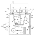
- FIG. 3 is a cross-sectional view of a chamber apparatus of a comparative example taken along a line perpendicular to the traveling direction of laser light.
- FIG. 4 is a view of the lower chamber seen from above.
- FIG. 5 is a view of the upper chamber as seen from above.
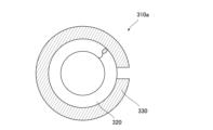
- FIG. 6 is a diagram showing a cross section perpendicular to the longitudinal direction of the metal seal.
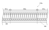
- FIG. 7 is a diagram showing a cross section of the metal seal taken along the longitudinal direction.
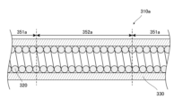
- FIG. 8 is a cross-sectional view taken along the longitudinal direction of a metal seal used in the discharge chamber for the gas laser apparatus of the first embodiment.
- FIG. 9 is a cross-sectional view taken along the longitudinal direction of a first modified example of the metal seal.
- FIG. 10 is a cross-sectional view taken along the longitudinal direction of a second modified example of the metal seal.
- FIG. 11 is a cross-sectional view taken along the longitudinal direction of a third modified example of the metal seal.
- FIG. 12 is a cross-sectional view taken along the longitudinal direction of a metal seal used in a discharge chamber for a gas laser apparatus according to the second embodiment.
- FIG. 13 is a diagram showing another modified example of the metal seal.
- FIG. 1 is a schematic diagram showing an example of the overall schematic configuration of an electronic device manufacturing apparatus used in an exposure process of an electronic device.
- the manufacturing apparatus used in the exposure process includes a gas laser apparatus 100 and an exposure apparatus 200.
- the exposure apparatus 200 includes an illumination optical system 210 including a plurality of mirrors 211, 212, and 213, and a projection optical system 220.
- the illumination optical system 210 illuminates a reticle pattern on a reticle stage RT with a laser beam incident from the gas laser apparatus 100.
- the projection optical system 220 reduces and projects the laser beam transmitted through the reticle to form an image on a workpiece (not shown) placed on a workpiece table WT.
- the workpiece is a photosensitive substrate such as a semiconductor wafer on which a photoresist is applied.
- the exposure apparatus 200 exposes the workpiece to laser beam reflecting the reticle pattern by synchronously moving the reticle stage RT and the workpiece table WT in parallel. By transferring a device pattern onto a semiconductor wafer through the above-described exposure process, a semiconductor device, which is an electronic device, can be manufactured.
- Comparative Example 2.1 Configuration A comparative example gas laser device 100 will be described. Note that the comparative example in the present disclosure is a configuration that the applicant recognizes as being known only by the applicant, and is not a publicly known example that the applicant recognizes.
- FIG. 2 is a schematic diagram showing an example of the overall schematic configuration of a gas laser device 100 of a comparative example.
- the gas laser device 100 is, for example, an ArF excimer laser device that uses a mixed gas containing argon (Ar), fluorine (F 2 ), and neon (Ne). This gas laser device 100 emits a laser beam with a central wavelength of about 193 nm.
- the gas laser device 100 may be a gas laser device other than an ArF excimer laser device, for example, a KrF excimer laser device that uses a mixed gas containing krypton (Kr), F 2 , and Ne. In this case, the gas laser device 100 emits a laser beam with a central wavelength of about 248 nm.
- a mixed gas containing Ar, F 2 , and Ne as a laser medium, or a mixed gas containing Kr, F 2 , and Ne as a laser medium, may be called a laser gas.
- the gas laser device 100 mainly comprises a housing 110, a laser oscillator 130 arranged in the internal space of the housing 110, a monitor module 160, a shutter 170, and a laser processor 190.
- FIG. 2 shows the internal structure of the chamber device 101 in a cross section along the direction of travel of the laser light.
- the left side of the paper along the direction of travel of the laser light may be referred to as the front side, the right side of the paper as the rear side, the top side of the paper as the upper side, and the bottom side of the paper as the lower side.
- the laser oscillator 130 mainly comprises a chamber device 101, a charger 141, a line narrowing module 145, an output coupling mirror 147, and a pulse compression circuit 150.
- FIG 3 is a cross-sectional view perpendicular to the direction of travel of the laser light in the chamber device 101.
- the chamber device 101 includes a discharge chamber 131, which encloses an internal space in which light is generated by excitation of the laser medium in the laser gas through discharge as described below.
- the discharge chamber 131 is a discharge chamber for a gas laser device.
- the discharge chamber 131 of the chamber device 101 in this example includes a chamber body 131M divided into an upper chamber 131a and a lower chamber 131b, and an electrically insulating plate 135 as a lid.
- the upper chamber 131a is a member having an opening 131H formed on its upper surface, and constitutes at least a part of the upper side of the discharge chamber 131.
- the lower chamber 131b is a member with a bottom, and constitutes at least a part of the lower side of the discharge chamber 131.
- the lower edge of the upper chamber 131a and the upper edge of the lower chamber 131b face each other, and the upper chamber 131a and the lower chamber 131b are combined.
- the upper chamber 131a and the lower chamber 131b enclose at least a portion of the internal space of the discharge chamber 131.
- Examples of materials for the upper chamber 131a and the lower chamber 131b include metals such as nickel-plated aluminum or nickel-plated stainless steel.
- Figure 4 is a view of the lower chamber 131b from above.
- the discharge chamber 131 has a generally rectangular cross section of the internal space in the horizontal direction.
- the upper edge of the lower chamber 131b surrounds a generally rectangular opening.
- a groove 132b is formed in the upper edge of the lower chamber 131b, and a metal seal 310b is disposed in the groove 132b. Therefore, the metal seal 310b also has a generally rectangular shape and includes a straight portion 351b and a curved portion 352b. In this example, the shape of the metal seal 310b is generally rectangular.
- the length of the straight portion 351b on the long side of the rectangle is, for example, approximately 800 mm, and the length of the straight portion 351b on the short side is, for example, approximately 300 mm.
- the length of the curved portion 352b is, for example, approximately 50 mm.
- the upper chamber 131a and the lower chamber 131b are fixed so as to be pressed against each other by a member not shown. This pressing force causes the metal seal 310b to deform so as to be crushed in the pressing direction, sealing the gap between the upper chamber 131a and the lower chamber 131b.
- the first chamber part and the second chamber part are combined with each other to enclose at least a part of the internal space of the discharge chamber 131, and the metal seal 310b seals the gap between the first chamber part and the second chamber part. Details of the metal seal 310b will be described later.
- the laser gas in the internal space of discharge chamber 131 is supplied from a laser gas supply source (not shown) through a pipe (not shown).
- the laser gas in discharge chamber 131 is subjected to a process such as removing F2 gas by a halogen filter, and is exhausted to housing 110 through a pipe (not shown) by an exhaust pump (not shown).
- the opening 131H in the upper chamber 131a of the chamber body 131M is blocked by an electrically insulating plate 135.
- the chamber body 131M and the electrically insulating plate 135 are combined with each other to enclose at least a portion of the internal space of the discharge chamber 131.
- Figure 5 is a view of the upper chamber 131a from above.
- the opening 131H is generally rectangular in shape.
- a groove 132a surrounding the opening 131H is formed on the upper surface of the upper chamber 131a, and a metal seal 310a is disposed within the groove 132a. Therefore, the metal seal 310a also has a generally rectangular shape and includes a straight portion 351a and a curved portion 352a.
- the shape of the metal seal 310a is generally rectangular.
- the length of the straight portion 351a on the long side of the rectangle is, for example, approximately 780 mm
- the length of the straight portion 351a on the short side is, for example, approximately 300 mm.
- the length of the curved portion 352a is, for example, approximately 80 mm.
- the chamber body 131M and the electrically insulating plate 135 are fixed so as to be pressed against each other by a member not shown. This pressing force causes the metal seal 310a to deform so as to be crushed in the pressing direction, sealing the gap between the chamber body 131M and the electrical insulating plate 135.
- the chamber body 131M and the electrical insulating plate 135 are the first and second chamber parts
- the first and second chamber parts are combined with each other to enclose at least a portion of the internal space of the discharge chamber 131, and the metal seal 310a seals the gap between the first and second chamber parts. Details of the metal seal 310a will be described later.
- the electrical insulating plate 135 includes an insulator.
- alumina ceramics which has low reactivity with F2 gas, can be used as the material of the electrical insulating plate 135.
- the electrical insulating plate 135 only needs to have electrical insulation properties, and examples of the material of the electrical insulating plate 135 include resins such as phenol resin and fluororesin, quartz, glass, etc.
- the first main electrode, electrode 134a, and the second main electrode, electrode 134b face each other at a distance, and are arranged such that their respective longitudinal directions are aligned along a predetermined direction that is the traveling direction of the laser light.
- electrode 134b is located directly above electrode 134a.
- the electrodes 134a and 134b are discharge electrodes for exciting the laser medium by glow discharge.
- electrode 134a is the anode
- electrode 134b is the cathode.
- the electrode holder part 137 is electrically connected to the chamber body 131M via wiring 137a.
- the electrode 134a is supported by and electrically connected to the electrode holder part 137.
- the electrode 134a is electrically connected to ground via the electrode holder part 137, wiring 137a, and the chamber body 131M.
- the electrode 134b is fixed to the surface of the electrically insulating plate 135 facing the internal space of the discharge chamber 131 by a current introduction terminal 157, which may be a bolt, for example.
- the current introduction terminal 157 is electrically connected to the pulse compression circuit 150 and other circuit components, which will be described later, and ensures electrical continuity between the pulse compression circuit 150 and the electrode 134b.
- the charger 141 is a high-voltage DC power supply that supplies electrical energy to the pulse compression circuit 150.
- the switch 151 is electrically connected to the charger 141 and is controlled by the laser processor 190. When the switch 151 is turned from OFF to ON, electrical energy from the charger 141 is supplied to the pulse compression circuit 150.
- the pulse compression circuit 150 is disposed on the holder 155, and generates a pulsed high voltage from the electrical energy held in the charger 141, and applies this high voltage between the electrodes 134a and 134b.
- the circuit between the pulse compression circuit 150 and the electrode 134a mainly comprises a number of peaking capacitors 153, a connection plate 152, and the above-mentioned current introduction terminal 157.
- the connection plate 152 is a conductive plate that connects the electrode 134b and the pulse compression circuit 150, and is made of a metal plate with a roughly U-shaped cross section perpendicular to the longitudinal direction.
- One terminal of each of the peaking capacitors 153 is electrically connected to the connection plate 152.
- the peaking capacitors 153 are, for example, ceramic capacitors whose dielectric material is strontium titanate or the like. Other examples of the dielectric material include barium titanate.
- a current introduction terminal 157 is electrically connected to the connection plate 152. In this way, one terminal of each of the multiple peaking capacitors 153 is electrically connected to one electrode 134b.
- each peaking capacitor 153 is electrically connected to the holder 155.
- the holder 155 is electrically connected to the discharge chamber 131. Therefore, the other terminal of each peaking capacitor 153 is electrically connected to ground. In addition, the other terminal of each peaking capacitor 153 is electrically connected to the other electrode 134a via the holder 155.
- a preionization electrode 180 is provided to the side of the electrode 134a on the electrode holder portion 137.
- the preionization electrode 180 includes a dielectric pipe 181, a preionization inner electrode 183, and a preionization outer electrode 185.
- the dielectric pipe 181 is, for example, a cylindrical pipe whose longitudinal direction is arranged along a predetermined direction.
- the dielectric pipe 181 is made of, for example, alumina ceramics or sapphire.
- the pre-ionization inner electrode 183 is rod-shaped and is arranged inside the dielectric pipe 181, extending along the longitudinal direction of the dielectric pipe 181.
- the pre-ionization inner electrode 183 is made of, for example, copper or brass.
- the pre-ionization outer electrode 185 is arranged between the dielectric pipe 181 and the electrode 134a, and extends along the longitudinal direction of the dielectric pipe 181. An end of the pre-ionization outer electrode 185 is in contact with the outer peripheral surface of the dielectric pipe 181.
- the pre-ionization outer electrode 185 does not need to be in contact with the outer peripheral surface of the dielectric pipe 181.
- the pre-ionization outer electrode 185 is fixed to a spacer 187 fixed to the electrode 134a.
- the preionization inner electrode 183 is electrically connected to the pulse compression circuit 150 via a preionization capacitor (not shown).
- the preionization outer electrode 185 is electrically connected to the electrode 134a via the electrode holder part 137, and is also electrically connected to the discharge chamber 131 via the electrode holder part 137 and the wiring 137a. Therefore, the preionization outer electrode 185 is electrically connected to ground.
- a high voltage is applied from the pulse compression circuit 150 to the preionization inner electrode 183 and the preionization outer electrode 185, causing a corona discharge to occur near the end of the preionization outer electrode 185. This corona discharge assists in the stable generation of a glow discharge between the electrodes 134a and 134b.
- a cross-flow fan 149 and a heat exchanger 148 are arranged on the opposite side of the electrode 134a side with respect to the electrode holder part 137 in the internal space of the discharge chamber 131.
- the space in which the cross-flow fan 149 and the heat exchanger 148 of the discharge chamber 131 are arranged is connected to the space between the electrodes 134a and 134b.
- the heat exchanger 148 is a radiator arranged beside the cross-flow fan 149 and connected to a pipe (not shown) through which a cooling medium flows.
- the cross-flow fan 149 is connected to a motor 149a arranged outside the discharge chamber 131 and rotates by the rotation of the motor 149a.
- the cross-flow fan 149 rotates, the laser gas sealed in the internal space of the discharge chamber 131 circulates as shown by the arrows in FIG. 3. At least a portion of the circulating laser gas passes through the heat exchanger 148, and the temperature of the laser gas is adjusted.
- a pair of windows 139a, 139b are provided on the wall of the discharge chamber 131.
- Window 139a is located at one end of the discharge chamber 131 in the direction of travel of the laser light
- window 139b is located at the other end of the discharge chamber 131 in the direction of travel
- the windows 139a, 139b sandwich the space between electrodes 134a, 134b.
- the windows 139a, 139b are inclined to form a Brewster angle with respect to the direction of travel of the laser light so as to suppress reflection of the laser light.
- the oscillating laser light is emitted to the outside of the discharge chamber 131 via the windows 139a, 139b.
- a pulsed high voltage is applied between electrodes 134a, 134b by the pulse compression circuit 150, so this laser light is a pulsed laser light.
- the line narrowing module 145 includes a housing 145a, a prism 145b arranged in the internal space of the housing 145a, a grating 145c, and a rotating stage (not shown). An opening is formed in the housing 145a, and the housing 145a is connected to the rear side of the discharge chamber 131 via the opening.
- Prism 145b expands the beam width of the light emitted from window 139a and makes the light incident on grating 145c. Prism 145b also reduces the beam width of the light reflected from grating 145c and returns the light to the internal space of discharge chamber 131 via window 139a. Prism 145b is supported on a rotating stage and rotates by the rotating stage. By rotating prism 145b, the angle of incidence of the light with respect to grating 145c is changed, and it is possible to select the wavelength of the light returning from grating 145c to discharge chamber 131 via prism 145b.
- Figure 2 shows an example in which one prism 145b is arranged, but it is sufficient that at least one prism is arranged.
- the surface of grating 145c is made of a highly reflective material, and has numerous grooves at regular intervals on the surface.
- the cross-sectional shape of each groove is, for example, a right-angled triangle.
- Grating 145c is Littrow-positioned so that the angle of incidence of light entering grating 145c from prism 145b matches the angle of diffraction of diffracted light of the desired wavelength. This allows light near the desired wavelength to be returned to discharge chamber 131 via prism 145b.
- the output coupling mirror 147 is disposed in the internal space of the optical path tube 147a connected to the front side of the discharge chamber 131, and faces the window 139b.
- the output coupling mirror 147 transmits part of the laser light emitted from the window 139b toward the monitor module 160, and reflects the other part back into the internal space of the discharge chamber 131 via the window 139b.
- the grating 145c and the output coupling mirror 147 form a Fabry-Perot type laser resonator.
- the monitor module 160 is disposed on the optical path of the laser light emitted from the output coupling mirror 147.
- the monitor module 160 includes a housing 161, and a beam splitter 163 and an optical sensor 165 disposed in the internal space of the housing 161.
- An opening is formed in the housing 161, and the internal space of the housing 161 communicates with the internal space of the optical path tube 147a through this opening.
- the beam splitter 163 transmits a portion of the laser light emitted from the output coupling mirror 147 toward the shutter 170, and reflects another portion of the laser light toward the light receiving surface of the optical sensor 165.
- the optical sensor 165 outputs a signal indicating the energy E of the laser light incident on the light receiving surface to the laser processor 190.
- the laser processor 190 of the present disclosure is a processing device including a storage device 190a in which a control program is stored, and a CPU (Central Processing Unit) 190b that executes the control program.
- the laser processor 190 is specially configured or programmed to execute the various processes included in the present disclosure.
- the laser processor 190 controls the entire gas laser device 100.
- the laser processor 190 transmits and receives various signals to and from the exposure processor 230 of the exposure device 200.
- the laser processor 190 receives signals indicating a light emission trigger Tr, which will be described later, and a target energy Et from the exposure processor 230.
- the target energy Et is a target value for the energy of the laser light used in the exposure process.
- the laser processor 190 controls the charging voltage of the charger 141 based on the energy E and the target energy Et received from the optical sensor 165 and the exposure processor 230.
- the energy of the laser light is controlled by controlling the charging voltage.
- the laser processor 190 is also electrically connected to the shutter 170, and controls the opening and closing of the shutter 170.
- the laser processor 190 closes the shutter 170 until the difference ⁇ E between the energy E received from the monitor module 160 and the target energy Et received from the exposure processor 230 falls within an allowable range.
- the laser processor 190 transmits a reception preparation completion signal to the exposure processor 230 to notify that the light emission trigger Tr is ready to receive.
- the exposure processor 230 receives the reception preparation completion signal, it transmits a signal indicating the light emission trigger Tr to the laser processor 190, and when the laser processor 190 receives the signal indicating the light emission trigger Tr, it opens the shutter 170.
- the light emission trigger Tr is a timing signal that causes the exposure processor 230 to cause the laser oscillator 130 to oscillate, and is an external trigger.
- the light emission trigger Tr may be specified by a predetermined repetition frequency f of the laser light and a predetermined number of pulses P.
- the repetition frequency f of the laser light is, for example, 100 Hz or more and 10 kHz or less.
- the shutter 170 is disposed on the optical path of the internal space of the optical path pipe 171 that communicates with an opening formed on the side opposite to the side to which the optical path pipe 147a is connected in the housing 161 of the monitor module 160.
- the internal spaces of the optical path pipes 171 and 147a and the internal spaces of the housings 161 and 145a are supplied with and filled with purge gas.
- the purge gas includes an inert gas such as nitrogen (N 2 ).
- the purge gas is supplied from a purge gas supply source (not shown) through a pipe (not shown).
- the optical path pipe 171 also communicates with the exposure device 200 through an opening of the housing 110 and an optical path pipe 500 that connects the housing 110 and the exposure device 200.
- the laser light that has passed through the shutter 170 enters the exposure device 200.
- the exposure processor 230 of the present disclosure is a processing device including a storage device in which a control program is stored, and a CPU that executes the control program.
- the exposure processor 230 is specially configured or programmed to execute the various processes included in the present disclosure.
- the exposure processor 230 also controls the entire exposure apparatus 200.
- the configuration of the metal seals 310b and 310a in this example will be described. Note that in this example, the metal seals 310b and 310a have roughly the same configuration, so only the metal seal 310a will be described.
- FIG. 6 is a diagram showing a cross section perpendicular to the longitudinal direction of metal seal 310a
- FIG. 7 is a diagram showing a cross section along the longitudinal direction of metal seal 310a.
- metal seal 310a of this example includes coil spring 320 and outer cover 330.
- Coil spring 320 is configured such that metal wire is formed in a spiral shape at a predetermined pitch.
- Outer cover 330 is a metal plate-shaped member processed so that the cross section perpendicular to the longitudinal direction has an approximately C-shape. Outer cover 330 generally surrounds the outer periphery of coil spring 320.
- the metal seal 310a arranged in the groove 132a is pressed radially by the electrical insulation plate 135 and the chamber body 131M, and as described above, is deformed so as to be crushed in the pressing direction, sealing the gap between the chamber body 131M and the electrical insulation plate 135.
- the metal seal 310b arranged in the groove 132b is pressed radially by the upper chamber 131a and the lower chamber 131b, and as described above, is deformed so as to be crushed in the pressing direction, sealing the gap between the upper chamber 131a and the lower chamber 131b.
- the internal spaces of the optical path tubes 147a, 171, and 500 and the internal spaces of the housings 145a and 161 are filled with purge gas from a purge gas supply source (not shown).
- Laser gas is supplied to the internal space of the discharge chamber 131 from a laser gas supply source (not shown).
- the laser processor 190 controls the motor 149a to rotate the cross-flow fan 149.
- the rotation of the cross-flow fan 149 circulates the laser gas in the internal space of the discharge chamber 131.
- the gap between the upper chamber 131a and the lower chamber 131b is sealed by the metal seal 310b, and the gap between the chamber body 131M and the electrical insulation plate 135 is sealed by the metal seal 310a, so that the laser gas is prevented from leaking outside the discharge chamber 131.
- the laser processor 190 receives a signal indicating the target energy Et and a signal indicating the light emission trigger Tr from the exposure processor 230.
- the laser processor 190 receives the signal indicating the target energy Et, it closes the shutter 170 and drives the charger 141.
- the laser processor 190 also turns on the switch 151 of the pulse compression circuit 150.
- the current from the charger 141 is charged to the peaking capacitor 153 via the pulse compression circuit 150.
- the peaking capacitor 153 is charged to a high potential in a short time.
- a pulsed high voltage is applied to the electrode 134b from the charger 141 and the peaking capacitor 153 via the current introduction terminal 157 for a short time.
- the timing at which a high voltage is applied between the pre-ionization inner electrode 183 and the pre-ionization outer electrode 185 is slightly earlier than the timing at which a high voltage is applied between the electrodes 134a and 134b.
- a corona discharge occurs near the ends of the dielectric pipe 181 and the preionization outer electrode 185, and ultraviolet light is emitted.
- the ultraviolet light irradiates the laser gas between the electrodes 134a and 134b, the laser gas between the electrodes 134a and 134b is preionized.
- a main discharge occurs between the electrodes 134a and 134b.
- This main discharge excites the laser medium contained in the laser gas between electrodes 134a and 134b, and emits light when the laser medium returns to its ground state.
- This light resonates between grating 145c and output coupling mirror 147, and the light is amplified each time it passes through the discharge space in the internal space of discharge chamber 131, causing laser oscillation.
- a portion of the resonating laser light passes through output coupling mirror 147 as pulsed laser light and proceeds to beam splitter 163.
- a portion of the laser light that reaches the beam splitter 163 is reflected by the beam splitter 163 and received by the optical sensor 165.
- the optical sensor 165 measures the energy E of the received laser light and outputs a signal indicating the energy E to the laser processor 190.
- the laser processor 190 controls the charging voltage so that the difference ⁇ E between the energy E and the target energy Et is within an acceptable range, and after the difference ⁇ E falls within the acceptable range, it transmits a reception preparation completion signal to the exposure processor 230 indicating that preparation for receiving the light emission trigger Tr is complete.
- the exposure processor 230 When the exposure processor 230 receives the ready to receive signal, it transmits a light emission trigger Tr to the laser processor 190.
- the laser processor 190 opens the shutter 170 in synchronization with the reception of the light emission trigger Tr, the laser light that passes through the shutter 170 enters the exposure device 200.
- This laser light is, for example, a pulsed laser light with a central wavelength of 193 nm.
- the metal seal 310a includes a straight portion 351a and a curved portion 352a.
- the curved portion 352a of the metal seal 310a tends to be less likely to be crushed in the pressing direction by the chamber main body 131M and the electrical insulating plate 135 than the straight portion 351a. If the metal seal 310a is not sufficiently crushed at the curved portion 352a, there is a concern that the distance between the electrical insulating plate 135 and the chamber main body 131M will differ from the design value. Therefore, there is a concern that the distance between the electrode 134b fixed to the electrical insulating plate 135 and the electrode 134a disposed on the electrode holder portion 137 will differ from the design value.
- the metal seal 310b includes a straight portion 351b and a curved portion 352b.
- the curved portion 352b of the metal seal 310b tends to be less likely to be crushed in the pressing direction by the upper chamber 131a and the lower chamber 131b than the straight portion 351b. If the curved portion 352b of the metal seal 310b is not sufficiently crushed, the distance between the upper chamber 131a and the lower chamber 131b may differ from the design value, and the relative position of the laser light emitted from the discharge chamber 131 with respect to the lower chamber 131b may differ from the design value. Therefore, if the curved portions 352a, 352b are not sufficiently crushed, there is a possibility that laser light different from the design value may be emitted.
- a discharge chamber 131 capable of emitting laser light according to the design value is exemplified.
- discharge chamber 131 is a discharge chamber for a gas laser device according to embodiment 1. Note that the same reference numerals are used for configurations similar to those described above, and duplicated descriptions will be omitted unless otherwise specified. In addition, in some drawings, for ease of viewing, some members may be omitted or simplified.
- FIG. 8 is a cross-sectional view along the longitudinal direction of the metal seal 310a used in the discharge chamber 131 of this embodiment.
- the metal seal 310a of this embodiment is different from the metal seal 310a of the comparative example in that, when the curved portion 352a is made straight, the winding pitch of the wire constituting the coil spring 320 at the curved portion 352a is larger than the winding pitch of the wire at the straight portion 351a. Therefore, in the metal seal 310a of this embodiment, the spring constant in the radial direction when the curved portion 352a is made straight is smaller than the spring constant in the radial direction of the straight portion 351a.
- the spring constant in the pressing direction when the curved portion 352a is made straight is smaller than the spring constant in the pressing direction of the straight portion 351a.
- the spring constant is the force applied to an object divided by the deformation amount of the object. Therefore, when the curved portion 352a is made straight, if a predetermined force is applied in the pressing direction, the curved portion 352a is crushed more than the straight portion 351a.
- adjacent wire rods constituting the coil spring 320 are in contact with each other without any gaps, and when the curved portion 352a is made straight, gaps are formed between adjacent wire rods of the curved portion 352a.
- the spring constant in the pressing direction of the curved portion 352a of the metal seal 310a is the same as the spring constant in the pressing direction of the straight portion 351a.
- FIG. 9 is a cross-sectional view along the longitudinal direction of the first modified example of the metal seal 310a.
- the winding pitch of the wire constituting the coil spring 320 in the curved portion 352a is larger than the winding pitch of the wire in the straight portion 351a
- the retainer 321 is disposed between the wire in the curved portion 352a.
- the retainer 321 is a plate-shaped member, and its size in the in-plane direction is smaller than the diameter of the coil spring 320. Therefore, in the pressing direction in which the metal seal 310a is pressed, a gap is formed between the retainer 321 and the outer skin 330. This prevents the retainer 321 from hindering the crushing of the metal seal 310a.
- An example of the material of the retainer 321 is resin.
- Figure 10 is a longitudinal cross-sectional view of a second modified example of metal seal 310a.
- the thickness of the wire constituting coil spring 320 in curved portion 352a is smaller than the thickness of the wire in straight portion 351a.
- the winding pitch of the wire in curved portion 352a is the same as the winding pitch of the wire in straight portion 351a.
- the winding pitch of the wire in curved portion 352a may be larger or smaller than the winding pitch of the wire in straight portion 351a.
- the spring constant in the pressing direction of curved portion 352a can be reduced regardless of the winding pitch of the wire.
- FIG. 11 is a longitudinal cross-sectional view of the third modified example of the metal seal 310a.
- the thickness and winding pitch of the wire constituting the coil spring 320 in the curved portion 352a are the same as those in the straight portion 351a.
- the wire materials in the straight portion 351a and the curved portion 352a are different from each other, and the Young's modulus of the wire constituting the coil spring 320 in the curved portion 352a is smaller than that of the wire in the straight portion 351a.
- the wire material in the curved portion 352a can be, for example, stainless steel, and the wire material in the straight portion 351a can be, for example, steel.
- the wires of different materials are connected to each other by, for example, welding.
- the metal seal 310b used in the discharge chamber 131 of this embodiment has a configuration generally similar to that of the metal seal 310a, so that in the metal seal 310b as well, when the curved portion 352b is made straight, the spring constant in the pressing direction is smaller than the spring constant in the pressing direction of the straight portion 351b.
- the spring constant in the pressing direction when the curved portions 352a, 352b of the metal seals 310a, 310b are made straight is smaller than the spring constant in the pressing direction of the straight portions 351a, 351b. Therefore, the metal seals 310a, 310b are more likely to be crushed at the curved portions 352a, 352b than when the spring constant in the pressing direction when the curved portions 352a, 352b are made straight is the same as the spring constant in the pressing direction of the straight portions 351a, 351b.
- the metal seal 310a is not sufficiently crushed at the curved portion 352a, so that the distance between the electrical insulating plate 135 and the chamber main body 131M is prevented from differing from the design value. Therefore, the distance between the electrodes 134b and 134a is prevented from differing from the design value. Furthermore, because curved portion 352b of metal seal 310b is not sufficiently crushed, the distance between upper chamber 131a and lower chamber 131b is prevented from differing from the design value, and the relative position of laser light emitted from discharge chamber 131 with respect to lower chamber 131b is prevented from differing from the design value. Therefore, according to discharge chamber 131 of the present embodiment, laser light can be emitted as designed.
- discharge chamber 131 is a discharge chamber for a gas laser apparatus according to embodiment 2. Note that the same reference numerals are used to designate components similar to those described above, and duplicated descriptions will be omitted unless otherwise specified.
- FIG. 12 is a cross-sectional view along the longitudinal direction of the metal seal 310a used in the discharge chamber 131 of this embodiment.
- the metal seal 310a of this embodiment is different from the metal seal 310a of the first embodiment in that it is composed of a metal tube 340.
- the thickness of the metal tube 340 at the curved portion 352a is smaller than the thickness of the metal tube 340 at the straight portion 351a. Therefore, the diameter of the inner peripheral surface of the metal tube 340 at the curved portion 352a is larger than the diameter of the inner peripheral surface of the metal tube 340 at the straight portion 351a.
- the spring constant in the radial direction when the curved portion 352a is made straight is smaller than the spring constant in the radial direction of the straight portion 351a. Therefore, in the metal seal 310a of this embodiment, the spring constant in the pressing direction when the curved portion 352a is made straight is smaller than the spring constant in the pressing direction of the straight portion 351a.
- the spring constant is the force applied to an object divided by the amount of deformation of the object. Therefore, in this embodiment as well, when the curved portion 352a is made straight and a predetermined force is applied in the pressing direction, the curved portion 352a collapses more than the straight portion 351a.
- the straight portion 351a and the curved portion 352a may be made of different materials for the metal tube 340, and the Young's modulus of the material for the metal tube 340 in the curved portion 352a may be smaller than the Young's modulus of the material for the metal tube 340 in the straight portion 351a.
- the material for the metal tube 340 in the curved portion 352a may be, for example, stainless steel
- the material for the metal tube 340 in the straight portion 351a may be, for example, steel.
- the metal tubes made of different materials are connected to each other by, for example, welding.
- the spring constant in the pressing direction of the curved portion 352a of the metal seal 310a is the same as the spring constant in the pressing direction of the straight portion 351a.
- the metal seal 310b has a configuration generally similar to that of the metal seal 310a. In the metal seal 310b of this embodiment as well, when the curved portion 352b is made straight, the spring constant in the pressing direction is smaller than the spring constant in the pressing direction of the straight portion 351b.
- laser light can be emitted according to the design values, similarly to the first embodiment.
- the thickness of the metal tube 340 may be constant in the straight portion 351a and the curved portion 352a, and the Young's modulus of the material constituting the metal tube 340 in the curved portion 352a may be smaller than the Young's modulus of the material constituting the metal tube 340 in the straight portion 351a.
- the present invention has been described above using an embodiment as an example, the present invention can be modified as appropriate.
- the configuration of the metal seals 310a and 310b may be different from that of the above embodiment, so long as the spring constant in the pressing direction when the curved portion 352a is made straight is smaller than the spring constant in the pressing direction of the straight portion 351a.
- the metal seals 310a and 310b are generally rectangular.
- the shape of the metal seals 310a and 310b does not have to be rectangular as long as it includes the straight portions 351a and 351b and the curved portions 352a and 352b.
- a modified example in which the shape of the metal seals 310a and 310b is other than rectangular will be described. FIG.
- the metal seal 310a has a racetrack shape including the straight portion 351a and the curved portion 352a.
- the shape of the metal seal 310b may also be a racetrack shape.
- metal seals 310a and 310b do not have to have a generally similar configuration. Specifically, for example, metal seal 310a may have the configuration of the above embodiment, and metal seal 310b may have a different configuration from the above embodiment.
- first chamber part and the second chamber part have been given as the upper chamber 131a and the lower chamber 131b, and the chamber body 131M and the electrically insulating plate 135.
- first chamber part and the second chamber part may be other parts as long as they are parts that, when combined with each other, enclose at least a portion of the internal space of the discharge chamber 131.
Landscapes
- Physics & Mathematics (AREA)
- Electromagnetism (AREA)
- Engineering & Computer Science (AREA)
- Plasma & Fusion (AREA)
- Optics & Photonics (AREA)
- Lasers (AREA)
Abstract
Description
2.比較例の説明
2.1 構成
2.2 動作
2.3 課題
3.実施形態1の説明
3.1 構成
3.2 作用・効果
4.実施形態2の説明
4.1 構成
4.2 作用・効果
図1は、電子デバイスの露光工程で使用される電子デバイスの製造装置の全体の概略構成例を示す模式図である。図1に示すように、露光工程で使用される製造装置は、ガスレーザ装置100及び露光装置200を含む。露光装置200は、複数のミラー211,212,213を含む照明光学系210と、投影光学系220とを含む。照明光学系210は、ガスレーザ装置100から入射するレーザ光によって、レチクルステージRTのレチクルパターンを照明する。投影光学系220は、レチクルを透過するレーザ光を、縮小投影してワークピーステーブルWT上に配置される不図示のワークピースに結像させる。ワークピースは、フォトレジストが塗布される半導体ウエハ等の感光基板である。露光装置200は、レチクルステージRTとワークピーステーブルWTとを同期して平行移動させることにより、レチクルパターンを反映するレーザ光をワークピースに露光する。以上のような露光工程によって半導体ウエハにデバイスパターンを転写することで電子デバイスである半導体デバイスを製造することができる。
2.1 構成
比較例のガスレーザ装置100について説明する。なお、本開示の比較例とは、出願人のみによって知られていると出願人が認識している形態であって、出願人が自認している公知例ではない。
次に、比較例のガスレーザ装置100の動作について説明する。
上記のように、メタルシール310aは、直線部351aと湾曲部352aとを含んでいる。メタルシール310aの湾曲部352aは、直線部351aに比べて、チャンバ本体131Mと電気絶縁プレート135とによる押圧方向に潰れにくい傾向にある。湾曲部352aにおいて、メタルシール310aが十分に潰れない場合、電気絶縁プレート135とチャンバ本体131Mとの距離が設計値と異なる懸念が生じる。このため、電気絶縁プレート135に固定される電極134bと、電極ホルダ部137上に配置される電極134aとの距離が設計値と異なる懸念が生じる。また、上記のように、メタルシール310bは、直線部351bと湾曲部352bとを含んでいる。メタルシール310bの湾曲部352bは、直線部351bに比べて、上側チャンバ131aと下側チャンバ131bとによる押圧方向に潰れにくい傾向にある。メタルシール310bの湾曲部352bが十分に潰れない場合、上側チャンバ131aと下側チャンバ131bとの距離が設計値と異なり、下側チャンバ131bに対する放電チャンバ131から出射するレーザ光の相対的な位置が設計値と異なる懸念が生じる。従って、湾曲部352a,352bが十分に潰れない場合、設計値と異なるレーザ光が出射する可能性がある。
次に、実施形態1のガスレーザ装置用放電チャンバである放電チャンバ131について説明する。なお、上記において説明した構成と同様の構成については同一の符号を付し、特に説明する場合を除き、重複する説明は省略する。また、一部の図面では、見易さのため、部材の一部を省略または簡略して記載する場合がある。
図8は、本実施形態の放電チャンバ131に用いられるメタルシール310aの長手方向に沿った断面図である。本実施形態のメタルシール310aは、湾曲部352aを直線状にした場合に、湾曲部352aにおけるコイルバネ320を構成する線材の巻ピッチが、直線部351aにおける線材の巻ピッチより大きい点において、比較例のメタルシール310aと異なる。従って、本実施形態のメタルシール310aでは、湾曲部352aを直線状にした場合における径方向のばね定数が、直線部351aの径方向のばね定数より小さい。メタルシール310aは、特定の径方向に押圧されて潰されるため、本実施形態のメタルシール310aでは、湾曲部352aを直線状にした場合における押圧方向のばね定数が、直線部351aの押圧方向のばね定数より小さい。ばね定数とは、物体に掛かる力を当該物体の変形量で除したものである。従って、湾曲部352aを直線状にした場合において、押圧方向に所定の力を加える場合、湾曲部352a潰れ方は、直線部351aの潰れ方よりも大きい。本例では、直線部351aにおいて、コイルバネ320を構成する互いに隣り合う線材同士が隙間なく接触しており、湾曲部352aを直線状にした場合に、湾曲部352aの互いに隣り合う線材間に隙間が形成されている。
本実施形態の放電チャンバ131では、メタルシール310a,310bにおける湾曲部352a,352bを直線状にした場合における押圧方向のばね定数が、直線部351a,351bの押圧方向のばね定数より小さい。このため、湾曲部352a,352bを直線状にした場合における押圧方向のばね定数と、直線部351a,351bの押圧方向のばね定数とが同じ場合と比べて、メタルシール310a,310bは、湾曲部352a,352bにおいて潰れやすい。従って、湾曲部352aにおいてメタルシール310aが十分に潰れないために電気絶縁プレート135とチャンバ本体131Mとの距離が設計値と異なることが抑制される。従って、電極134bと電極134aとの距離が設計値と異なることが抑制される。また、メタルシール310bの湾曲部352bが十分に潰れないために上側チャンバ131aと下側チャンバ131bとの距離が設計値と異なることが抑制され、放電チャンバ131から出射するレーザ光の下側チャンバ131bに対する相対的な位置が設計値と異なることが抑制される。従って、本実施形態の放電チャンバ131によれば、設計値通りにレーザ光が出射し得る。
次に、実施形態2のガスレーザ装置用放電チャンバである放電チャンバ131について説明する。なお、上記において説明した構成と同様の構成については同一の符号を付し、特に説明する場合を除き、重複する説明は省略する。
図12は、本実施形態の放電チャンバ131に用いられるメタルシール310aの長手方向に沿った断面図である。図12に示すように、本実施形態のメタルシール310aは、金属管340から構成される点において、実施形態1のメタルシール310aと異なる。本実施形態では、湾曲部352aにおける金属管340の肉厚は、直線部351aにおける金属管340の肉厚より小さい。従って、湾曲部352aにおける金属管340の内周面の直径は、直線部351aにおける金属管340の内周面の直径よりも大きい。従って、本実施形態のメタルシール310aでは、湾曲部352aを直線状にした場合における径方向のばね定数が、直線部351aの径方向のばね定数より小さい。このため、本実施形態のメタルシール310aでは、湾曲部352aを直線状にした場合における押圧方向のばね定数が、直線部351aの押圧方向のばね定数より小さい。上記のように、ばね定数とは、物体に掛かる力を当該物体の変形量で除したものであるため、本実施形態においても、湾曲部352aを直線状にした場合において、押圧方向に所定の力を加える場合、湾曲部352a潰れ方は、直線部351aの潰れ方よりも大きい。
本実施形態の放電チャンバ131においても、実施形態1と同様に設計値通りにレーザ光が出射し得る。
Claims (14)
- 内部空間に互いに間隔をあけて対向する一対の放電電極が配置され、レーザガスが封入されるガスレーザ装置用放電チャンバであって、
互いに組み合わされることで前記内部空間の少なくとも一部を囲う第1チャンバ部品及び第2チャンバ部品と、
直線部と湾曲部とを含み、前記第1チャンバ部品と前記第2チャンバ部品との間に配置され、前記第1チャンバ部品と前記第2チャンバ部品とに押圧されて、前記第1チャンバ部品と前記第2チャンバ部品との隙間を封止するメタルシールと、
を備え、
前記メタルシールの前記湾曲部を直線状にした場合における押圧方向のばね定数は、前記直線部の前記押圧方向のばね定数より小さい
ガスレーザ装置用放電チャンバ。 - 請求項1に記載のガスレーザ装置用放電チャンバであって、
前記メタルシールは、金属の外皮と、
前記外皮に囲われるコイルバネと、
を含む。 - 請求項2に記載のガスレーザ装置用放電チャンバであって、
前記湾曲部における前記コイルバネを構成する線材の巻ピッチは、前記直線部における前記巻ピッチより大きい。 - 請求項3に記載のガスレーザ装置用放電チャンバであって、
前記湾曲部における前記線材間にリテーナが配置される。 - 請求項4に記載のガスレーザ装置用放電チャンバであって、
前記リテーナは樹脂から成る。 - 請求項2に記載のガスレーザ装置用放電チャンバであって、
前記湾曲部における前記コイルバネを構成する線材の太さは、前記直線部における前記線材の太さより小さい。 - 請求項2に記載のガスレーザ装置用放電チャンバであって、
前記湾曲部における前記コイルバネを構成する線材のヤング率は、前記直線部における前記線材のヤング率より小さい。 - 請求項7に記載のガスレーザ装置用放電チャンバであって、
前記湾曲部における前記線材は、ステンレス鋼であり、
前記直線部における前記線材は、鋼である。 - 請求項1に記載のガスレーザ装置用放電チャンバであって、
前記メタルシールは、金属管から成り、
前記湾曲部における前記金属管の肉厚は、前記直線部における前記肉厚より小さい。 - 請求項1に記載のガスレーザ装置用放電チャンバであって、
前記メタルシールの前記湾曲部における押圧方向のばね定数は、前記直線部の押圧方向のばね定数と同じである。 - 請求項1に記載のガスレーザ装置用放電チャンバであって、
前記第1チャンバ部品は前記ガスレーザ装置用放電チャンバの上側の少なくとも一部を構成する上側チャンバであり、前記第2チャンバ部品は前記ガスレーザ装置用放電チャンバの下側の少なくとも一部を構成する下側チャンバである。 - 請求項1に記載のガスレーザ装置用放電チャンバであって、
前記第1チャンバ部品は前記ガスレーザ装置用放電チャンバの本体を構成し上部に開口を有するチャンバ本体であり、前記第2チャンバ部品は前記開口を塞ぐ蓋体である。 - 請求項12に記載のガスレーザ装置用放電チャンバであって、
前記蓋体は、一方の前記放電電極が固定される絶縁プレートである。 - 内部空間に互いに間隔をあけて対向する一対の放電電極が配置され、レーザガスが封入されるガスレーザ装置用放電チャンバであって、
互いに組み合わされることで前記内部空間の少なくとも一部を囲う第1チャンバ部品及び第2チャンバ部品と、
直線部と湾曲部とを含み、前記第1チャンバ部品と前記第2チャンバ部品との間に配置され、前記第1チャンバ部品と前記第2チャンバ部品とに押圧されて、前記第1チャンバ部品と前記第2チャンバ部品との隙間を封止するメタルシールと、
を備え、
前記メタルシールの前記湾曲部を直線状にした場合における押圧方向のばね定数は、前記直線部の前記押圧方向のばね定数より小さいガスレーザ装置用放電チャンバを含むガスレーザ装置によってレーザ光を生成し、
前記レーザ光を露光装置に出力し、
電子デバイスを製造するために、前記露光装置内で感光基板上に前記レーザ光を露光すること
を含む電子デバイスの製造方法。
Priority Applications (4)
| Application Number | Priority Date | Filing Date | Title |
|---|---|---|---|
| PCT/JP2023/002744 WO2024157484A1 (ja) | 2023-01-27 | 2023-01-27 | ガスレーザ装置用放電チャンバ、及び電子デバイスの製造方法 |
| CN202380083212.8A CN120303840A (zh) | 2023-01-27 | 2023-01-27 | 气体激光装置用放电腔以及电子器件的制造方法 |
| JP2024572815A JPWO2024157484A1 (ja) | 2023-01-27 | 2023-01-27 | |
| US19/226,440 US20250300418A1 (en) | 2023-01-27 | 2025-06-03 | Discharge chamber for gas laser apparatus and electronic device manufacturing method |
Applications Claiming Priority (1)
| Application Number | Priority Date | Filing Date | Title |
|---|---|---|---|
| PCT/JP2023/002744 WO2024157484A1 (ja) | 2023-01-27 | 2023-01-27 | ガスレーザ装置用放電チャンバ、及び電子デバイスの製造方法 |
Related Child Applications (1)
| Application Number | Title | Priority Date | Filing Date |
|---|---|---|---|
| US19/226,440 Continuation US20250300418A1 (en) | 2023-01-27 | 2025-06-03 | Discharge chamber for gas laser apparatus and electronic device manufacturing method |
Publications (1)
| Publication Number | Publication Date |
|---|---|
| WO2024157484A1 true WO2024157484A1 (ja) | 2024-08-02 |
Family
ID=91970154
Family Applications (1)
| Application Number | Title | Priority Date | Filing Date |
|---|---|---|---|
| PCT/JP2023/002744 Ceased WO2024157484A1 (ja) | 2023-01-27 | 2023-01-27 | ガスレーザ装置用放電チャンバ、及び電子デバイスの製造方法 |
Country Status (4)
| Country | Link |
|---|---|
| US (1) | US20250300418A1 (ja) |
| JP (1) | JPWO2024157484A1 (ja) |
| CN (1) | CN120303840A (ja) |
| WO (1) | WO2024157484A1 (ja) |
Citations (7)
| Publication number | Priority date | Publication date | Assignee | Title |
|---|---|---|---|---|
| JPS52130682U (ja) * | 1976-03-31 | 1977-10-04 | ||
| US5048041A (en) * | 1988-01-15 | 1991-09-10 | Cymer Laser Technologies | Compact excimer laser |
| JPH09246637A (ja) * | 1996-03-07 | 1997-09-19 | Tadahiro Omi | レーザービームチャンバーおよびその作成方法 |
| US20050083984A1 (en) * | 2003-10-17 | 2005-04-21 | Igor Bragin | Laser system sealing |
| WO2008156031A1 (ja) * | 2007-06-19 | 2008-12-24 | Tokyo Electron Limited | 真空処理装置 |
| WO2019207630A1 (ja) * | 2018-04-23 | 2019-10-31 | ギガフォトン株式会社 | レーザチャンバ、シール部材の製造方法、及び電子デバイスの製造方法 |
| JP2022073477A (ja) * | 2020-11-02 | 2022-05-17 | 株式会社東芝 | 高周波加速空洞及び高周波加速器システム |
-
2023
- 2023-01-27 WO PCT/JP2023/002744 patent/WO2024157484A1/ja not_active Ceased
- 2023-01-27 CN CN202380083212.8A patent/CN120303840A/zh active Pending
- 2023-01-27 JP JP2024572815A patent/JPWO2024157484A1/ja active Pending
-
2025
- 2025-06-03 US US19/226,440 patent/US20250300418A1/en active Pending
Patent Citations (7)
| Publication number | Priority date | Publication date | Assignee | Title |
|---|---|---|---|---|
| JPS52130682U (ja) * | 1976-03-31 | 1977-10-04 | ||
| US5048041A (en) * | 1988-01-15 | 1991-09-10 | Cymer Laser Technologies | Compact excimer laser |
| JPH09246637A (ja) * | 1996-03-07 | 1997-09-19 | Tadahiro Omi | レーザービームチャンバーおよびその作成方法 |
| US20050083984A1 (en) * | 2003-10-17 | 2005-04-21 | Igor Bragin | Laser system sealing |
| WO2008156031A1 (ja) * | 2007-06-19 | 2008-12-24 | Tokyo Electron Limited | 真空処理装置 |
| WO2019207630A1 (ja) * | 2018-04-23 | 2019-10-31 | ギガフォトン株式会社 | レーザチャンバ、シール部材の製造方法、及び電子デバイスの製造方法 |
| JP2022073477A (ja) * | 2020-11-02 | 2022-05-17 | 株式会社東芝 | 高周波加速空洞及び高周波加速器システム |
Also Published As
| Publication number | Publication date |
|---|---|
| US20250300418A1 (en) | 2025-09-25 |
| CN120303840A (zh) | 2025-07-11 |
| JPWO2024157484A1 (ja) | 2024-08-02 |
Similar Documents
| Publication | Publication Date | Title |
|---|---|---|
| US12347995B2 (en) | Chamber device, gas laser device, and electronic device manufacturing method | |
| US20240405497A1 (en) | Chamber of gas laser apparatus and electronic device manufacturing method | |
| WO2024157484A1 (ja) | ガスレーザ装置用放電チャンバ、及び電子デバイスの製造方法 | |
| US20240399510A1 (en) | Method of baking chamber of gas laser apparatus and electronic device manufacturing method | |
| US20240339797A1 (en) | Gas laser device and electronic device manufacturing method | |
| US20230108886A1 (en) | Gas laser apparatus and electronic device manufacturing method | |
| US20250293478A1 (en) | Chamber apparatus for laser, gas laser apparatus, and electronic device manufacturing method | |
| US20250329978A1 (en) | Chamber apparatus for laser, gas laser apparatus, and electronic device manufacturing method | |
| US20250309605A1 (en) | Chamber device, gas laser device, and electronic device manufacturing method | |
| US20250233378A1 (en) | Chamber of gas laser apparatus, gas laser apparatus, and electronic device manufacturing method | |
| US20240405501A1 (en) | Gas laser device and electronic device manufacturing method | |
| CN116097532B (zh) | 窄带化模块、气体激光装置和电子器件的制造方法 | |
| US20240405496A1 (en) | Chamber for gas laser device, gas laser device, and electronic device manufacturing method | |
| US20250337210A1 (en) | Chamber device of gas laser apparatus, gas laser apparatus, and electronic device manufacturing method | |
| WO2024009662A1 (ja) | ガスレーザ装置のチャンバ、ガスレーザ装置、及び電子デバイスの製造方法 | |
| JP7847655B2 (ja) | ガスレーザ装置及び電子デバイスの製造方法 | |
| US20260066606A1 (en) | Gas laser device and electronic device manufacturing method | |
| US12327975B2 (en) | Chamber device, and electronic device manufacturing method | |
| US20260106425A1 (en) | Gas laser device and electronic device manufacturing method | |
| CN120677601A (zh) | 气体激光装置以及电子器件的制造方法 | |
| WO2023218548A1 (ja) | 放電電極、アノードの製造方法、及び電子デバイスの製造方法 |
Legal Events
| Date | Code | Title | Description |
|---|---|---|---|
| 121 | Ep: the epo has been informed by wipo that ep was designated in this application |
Ref document number: 23918444 Country of ref document: EP Kind code of ref document: A1 |
|
| WWE | Wipo information: entry into national phase |
Ref document number: 202380083212.8 Country of ref document: CN |
|
| WWE | Wipo information: entry into national phase |
Ref document number: 2024572815 Country of ref document: JP |
|
| WWP | Wipo information: published in national office |
Ref document number: 202380083212.8 Country of ref document: CN |
|
| NENP | Non-entry into the national phase |
Ref country code: DE |
|
| 122 | Ep: pct application non-entry in european phase |
Ref document number: 23918444 Country of ref document: EP Kind code of ref document: A1 |