WO2024154429A1 - 測距装置 - Google Patents
測距装置 Download PDFInfo
- Publication number
- WO2024154429A1 WO2024154429A1 PCT/JP2023/041827 JP2023041827W WO2024154429A1 WO 2024154429 A1 WO2024154429 A1 WO 2024154429A1 JP 2023041827 W JP2023041827 W JP 2023041827W WO 2024154429 A1 WO2024154429 A1 WO 2024154429A1
- Authority
- WO
- WIPO (PCT)
- Prior art keywords
- light
- interference
- bank
- unit
- distance measuring
- Prior art date
- Legal status (The legal status is an assumption and is not a legal conclusion. Google has not performed a legal analysis and makes no representation as to the accuracy of the status listed.)
- Ceased
Links
Images



















Classifications
-
- G—PHYSICS
- G01—MEASURING; TESTING
- G01C—MEASURING DISTANCES, LEVELS OR BEARINGS; SURVEYING; NAVIGATION; GYROSCOPIC INSTRUMENTS; PHOTOGRAMMETRY OR VIDEOGRAMMETRY
- G01C3/00—Measuring distances in line of sight; Optical rangefinders
- G01C3/02—Details
- G01C3/06—Use of electric means to obtain final indication
-
- G—PHYSICS
- G01—MEASURING; TESTING
- G01S—RADIO DIRECTION-FINDING; RADIO NAVIGATION; DETERMINING DISTANCE OR VELOCITY BY USE OF RADIO WAVES; LOCATING OR PRESENCE-DETECTING BY USE OF THE REFLECTION OR RERADIATION OF RADIO WAVES; ANALOGOUS ARRANGEMENTS USING OTHER WAVES
- G01S7/00—Details of systems according to groups G01S13/00, G01S15/00, G01S17/00
- G01S7/48—Details of systems according to groups G01S13/00, G01S15/00, G01S17/00 of systems according to group G01S17/00
- G01S7/483—Details of pulse systems
- G01S7/486—Receivers
- G01S7/4861—Circuits for detection, sampling, integration or read-out
- G01S7/4863—Detector arrays, e.g. charge-transfer gates
-
- G—PHYSICS
- G01—MEASURING; TESTING
- G01S—RADIO DIRECTION-FINDING; RADIO NAVIGATION; DETERMINING DISTANCE OR VELOCITY BY USE OF RADIO WAVES; LOCATING OR PRESENCE-DETECTING BY USE OF THE REFLECTION OR RERADIATION OF RADIO WAVES; ANALOGOUS ARRANGEMENTS USING OTHER WAVES
- G01S7/00—Details of systems according to groups G01S13/00, G01S15/00, G01S17/00
- G01S7/48—Details of systems according to groups G01S13/00, G01S15/00, G01S17/00 of systems according to group G01S17/00
- G01S7/495—Counter-measures or counter-counter-measures using electronic or electro-optical means
-
- G—PHYSICS
- G01—MEASURING; TESTING
- G01S—RADIO DIRECTION-FINDING; RADIO NAVIGATION; DETERMINING DISTANCE OR VELOCITY BY USE OF RADIO WAVES; LOCATING OR PRESENCE-DETECTING BY USE OF THE REFLECTION OR RERADIATION OF RADIO WAVES; ANALOGOUS ARRANGEMENTS USING OTHER WAVES
- G01S7/00—Details of systems according to groups G01S13/00, G01S15/00, G01S17/00
- G01S7/48—Details of systems according to groups G01S13/00, G01S15/00, G01S17/00 of systems according to group G01S17/00
- G01S7/497—Means for monitoring or calibrating
Definitions
- This technology relates to a distance measuring device. More specifically, this technology relates to a distance measuring device capable of detecting interference light.
- Range measuring devices are used for various purposes such as in-vehicle equipment, transport equipment, and mobile equipment.
- various types of interference light such as sudden interference light, persistent interference light, and intentional interference light
- a distance measuring sensor has been proposed in which the light-emitting element is made to emit light during a first light-receiving period and the light-receiving element receives the returned light, and in a second light-receiving period, the light-emitting element is not made to emit light and the light-receiving element receives the light, thereby acquiring disturbance information (see, for example, Patent Document 1).
- the first light receiving period during which the light emitting element emits light and the second light receiving period during which the light emitting element does not emit light are periodically divided. This increases the discrepancy between the timing of receiving the return light and the timing of receiving the interference light, and there is a risk that the sudden incidence of interference light cannot be handled.
- This technology was developed in light of these circumstances, and aims to reduce the discrepancy between the timing of receiving the distance measurement light and the timing of receiving the interference light.
- This technology has been made to solve the above-mentioned problems, and its first aspect is a distance measuring device that includes a light emitting unit that emits distance measuring light, and a light receiving unit that has multiple light receiving areas that can receive light by switching between receiving and not receiving reflected light of the distance measuring light. This enables distance measuring based on light reception in multiple light receiving areas, while simultaneously receiving light used for distance measuring and light used for interference detection.
- the light receiving region may include a first light receiving region and a second light receiving region in which the presence or absence of reception of the reflected light can be switched exclusively between each other, and the positions of the first light receiving region and the second light receiving region may be set so that when the reflected light is received in the first light receiving region, the reflected light is not received in the second light receiving region, and the positions of the first light receiving region and the second light receiving region may be set so that when the reflected light is received in the second light receiving region, the reflected light is not received in the first light receiving region.
- the light emitting unit may include a first laser element corresponding to the first light receiving region and a second laser element corresponding to the second light receiving region, and when the reflected light is received in the first light receiving region, the first laser element may be turned on and the second laser element may be turned off, and when the reflected light is received in the second light receiving region, the first laser element may be turned off and the second laser element may be turned on. This provides the effect of simultaneously emitting distance measurement light during distance measurement and not emitting distance measurement light during interference detection.
- a control unit may be further provided that controls a distance measurement operation based on reception of the reflected light and an interference detection operation based on reception of interference light that interferes with the reflected light. This provides the effect of carrying out the distance measurement operation and the interference detection operation in cooperation with each other.
- control unit may repeat the distance measurement operation and the interference detection operation on a subframe basis. This brings about the effect that in each of the first light receiving region and the second light receiving region, reception of reflected light and reception of light used for interference detection are performed for each subframe.
- control unit may change the emission interval of the distance measuring light based on the detection result of the interference light. This brings about the effect of reducing the interference effect caused by the interference light.
- control unit may randomly change the emission interval of the distance measuring light based on the detection result of the interference light. This brings about the effect of irregularly reducing the interference effect caused by the interference light.
- control unit may detect the interference light based on the presence or absence of a peak in a histogram showing the relationship between the light reception frequency in the light receiving area and the distance, or based on an interference evaluation index. This provides the effect of detecting interference light based on non-reception of reflected light.
- control unit may issue an interference flag indicating the presence or absence of interference based on the detection result of the interference light. This provides the effect of notifying the detection of interference light.
- the first light receiving area and the second light receiving area may each be provided in a plurality of areas, and the first light receiving area and the second light receiving area may be switched for each frame and used for distance measurement and interference detection. This provides the effect that the first light receiving area and the second light receiving area are changed for each frame.
- the first light receiving region and the second light receiving region may each be provided in a plurality of regions, and at least a portion of the first light receiving region and the second light receiving region may be selected and used for distance measurement and interference detection. This provides the effect of changing the resolution and exposure time based on the selection of the first light receiving region and the second light receiving region.
- At least a portion of the first light receiving area and the second light receiving area used for the distance measurement and the interference detection may be selected randomly. This brings about the effect of making the selection of the first light receiving area and the second light receiving area irregular.
- control unit may use the detection result of the interference light in the first frame to remove noise in the second frame. This provides the effect of using interference detection to remove noise.
- the second aspect is a distance measuring device that includes a light emitting unit that emits distance measuring light, a light receiving unit that receives the reflected light of the distance measuring light, and a control unit that randomly changes the emission interval of the distance measuring light based on the detection result of the interference light. This brings about the effect of interrupting the interference action without performing interference detection.
- the third aspect is a distance measuring device that includes a light emitting unit that emits distance measuring light based on a light emitting trigger, a light receiving unit that receives light reflected from the distance measuring light, and a control unit that controls the detection of light received by the light receiving unit based on non-light emitting timings that are provided between light emitting timings based on the light emitting trigger. This provides the effect of performing interference detection based on light reception at non-light emitting timings that are provided between light emitting timings.
- control unit may control the setting of a light emission period including the light emission timing and a non-light emission period including the non-light emission timing. This brings about the effect that the timing of distance measurement and interference detection can be changed.
- the light emission period may be set based on a slot unit, which is a unit of emission of one light emission pulse emitted from the light emitting unit or a unit of generation of a histogram of the number of times light is received by the light receiving unit. This provides the effect of performing distance measurement and interference detection multiple times per frame.
- control unit may notify the detection result of interference light interfering with the distance measurement light. This brings about an effect that the detection result of the interference light can be confirmed externally.
- control unit may calculate distance measurement data based on the received light in response to the emission at the emission timing, and correct the distance measurement data based on the detection result of the interference light detected based on the non-emission timing. This has the effect of reducing the effect of the interference light on the distance measurement light.
- control unit may set the sampling accuracy of the signal based on the non-emission timing to be lower than the sampling accuracy of the signal based on the emission timing. This provides the effect of achieving low power consumption while suppressing deterioration in distance measurement accuracy.
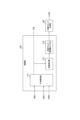
- FIG. 1 is a block diagram showing an example of the configuration of a distance measuring device according to a first embodiment
- FIG. 2 is a block diagram showing a configuration example of a light detection unit according to the first embodiment
- FIG. 2 is a block diagram showing a configuration example of a control unit according to the first embodiment.
- 1 is a block diagram illustrating an example of a configuration of an imaging apparatus according to a first embodiment.
- 1 is a block diagram illustrating an example of a configuration of a solid-state imaging device according to a first embodiment.
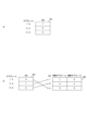
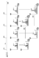
- FIG. 4 illustrates an example of bank switching according to the first embodiment
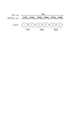
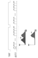
- 5 is a timing chart showing a distance measuring operation and an interference detection operation according to the first embodiment.
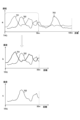
- 5A to 5C are diagrams illustrating a process of generating distance measurement data and interference detection data according to the first embodiment.
- 5 is a timing chart showing an example of data output associated with distance measurement and interference detection according to the first embodiment.
- 6A to 6C are diagrams illustrating an example of a light emission pattern when switching between banks according to the first embodiment.
- 11A and 11B are diagrams illustrating an example of a light receiving pattern when a bank is switched according to the first embodiment.
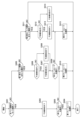
- 10 is a flowchart illustrating an example of an interference detection process according to the first embodiment.
- FIG. 13 is a timing chart showing a distance measuring operation and an interference detection operation according to the third embodiment.
- FIG. 13 is a block diagram illustrating an example of a configuration of a histogram calculation unit according to a third embodiment.
- 13 is a timing chart showing an example of a method for changing a laser interval according to a fourth embodiment.
- 13 is a timing chart showing an example of a bank switching method according to a fifth embodiment.
- FIG. 23 illustrates a first example of a bank switching method according to the fifth embodiment;
- FIG. 23 is a block diagram illustrating a first example of a bank switching unit according to the fifth embodiment.
- FIG. 23 is a diagram illustrating a second example of a bank transition table according to the fifth embodiment.
- FIG. 13 is a timing chart showing a second example of a bank transition method according to the fifth embodiment.
- FIG. 23 is a block diagram illustrating a second example of a bank switching unit according to the fifth embodiment. 13 is a flowchart showing a bank transition method according to a fifth embodiment.
- FIG. 23 is a diagram illustrating an example of a bank selection method according to the sixth embodiment. 23 is a timing chart showing an example of transition of an interference flag referred to in bank selection according to the sixth embodiment;
- FIG. 23 is a diagram illustrating a bank selection method based on a transition of an interference flag according to a sixth embodiment.
- 23 is a timing chart showing a distance measuring operation according to the seventh embodiment. 23 is a flowchart showing a distance measuring operation according to the seventh embodiment.
- 23 is a block diagram illustrating an example of the configuration of an imaging apparatus according to an eighth embodiment.
- 13A to 13C are diagrams illustrating a method of generating a histogram based on a light emission trigger and a non-light emission trigger in the eighth embodiment.
- 13A to 13C are diagrams illustrating an interference correction method according to an eighth embodiment.
- 23 is a timing chart showing a sampling method based on a light emission trigger and a non-light emission trigger according to a ninth embodiment.
- 23 is a timing chart showing a sampling method based on a light emission trigger and a non-light emission trigger according to a tenth embodiment.
- 23 is a timing chart showing a sampling method based on a light emission trigger and a non-light emission trigger according to an eleventh embodiment.
- FIG. 23 is a timing chart showing a sampling method based on a light emission trigger and a non-light emission trigger according to a twelfth embodiment.
- FIG. 23 is a diagram showing an example of a sampling method of interference data according to the thirteenth embodiment;
- FIG. 23 is a diagram illustrating an example of a sampling method of interference data according to the fourteenth embodiment.
- FIG. 23 is a block diagram illustrating an example of the configuration of an imaging apparatus according to a fifteenth embodiment.
- FIG. 23 is a block diagram showing an example of the configuration of an imaging apparatus according to a sixteenth embodiment.
- FIG. 23 is a perspective view showing an example of a stack of layers in a solid-state imaging device according to a seventeenth embodiment.
- FIG. 23 is a perspective view showing an example of a stack of layers in a solid-state imaging device according to a seventeenth embodiment.
- FIG. 23 is a perspective view showing an example of a stack of a pixel array unit according to an eighteenth embodiment
- FIG. 23 is a perspective view showing an example of a stack of a pixel array unit according to a nineteenth embodiment
- 1 is a block diagram showing a schematic configuration example of a vehicle control system
- FIG. 4 is an explanatory diagram showing an example of an installation position of an imaging unit.
- First embodiment an example in which a bank for distance measurement and a bank for interference detection are switched for each subframe, and distance measurement based on reflected light and interference detection based on interference light are performed simultaneously
- Second embodiment example in which a plurality of banks for performing distance measurement and a plurality of banks for performing interference detection are provided, and the bank for performing distance measurement and the bank for performing interference detection are switched between each other
- Third embodiment example in which detected interference light is used for noise subtraction in distance measurement
- Fourth embodiment (example of randomly changing the PRI (Pulse Repetition Interval) of distance measuring light regardless of the presence or absence of interference light) 5.
- Fifth embodiment (an example in which a plurality of banks for performing distance measurement and a plurality of banks for performing interference detection are provided, and the bank for performing distance measurement and the bank for performing interference detection are randomly switched) 6.
- Sixth embodiment (an example in which a plurality of banks for performing distance measurement and a plurality of banks for performing interference detection are provided, and the bank for performing distance measurement and the bank for performing interference detection are selectable) 7.
- Seventh embodiment (example of randomly changing PRI of distance measurement light without performing interference detection) 8.
- Eighth embodiment (example of performing interference detection based on non-light emitting triggers inserted between light emitting triggers) 9.
- Ninth embodiment (example of generating multiple light emission triggers between non-light emission triggers) 10.
- Tenth embodiment (example of randomly generating light emission triggers and non-light emission triggers) 11.
- Eleventh embodiment (an example of generating a sequence of light emission triggers and non-light emission triggers based on a histogram generation unit) 12.
- Twelfth embodiment (example of switching between light emission trigger series and non-light emission trigger series for each histogram generation unit) 13.
- Thirteenth embodiment (example of dividing measurable distance to generate a histogram based on a light emission trigger and a histogram based on a non-light emission trigger) 14.
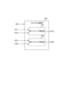
- FIG. 1 is a block diagram showing an example of the configuration of a distance measuring device according to a first embodiment.
- the distance measuring device 100 captures a distance image based on, for example, ToF (Time of Flight).
- the distance image can be generated from a distance pixel signal based on the distance for each pixel in the depth direction from the distance measuring device 100 to the object 101.
- the distance measuring device 100 can emit distance measuring light LML to the object 101 and perform distance measurement based on receiving reflected light LRF from which the distance measuring light LML is reflected.
- interference light LIF emitted from the interference source 102 may be incident on the distance measuring device 100.
- the distance measuring device 100 performs interference detection of the interference light LIF, and when the interference light LIF is detected, it can operate to reduce the influence of the interference light LIF interfering with the distance measuring light LML.
- the distance measuring device 100 includes a drive unit 111, a light emitting unit 112, a light detecting unit 123, optical systems 113 and 121, and an optical filter 122.
- the driving unit 111 drives the light-emitting unit 112 according to instructions from the light detection unit 123. At this time, the driving unit 111 sets the drive timing of the light-emitting unit 112 according to a light emission trigger TRG from the light detection unit 123. The driving unit 111 also sets the light-emitting area of the light-emitting unit 112 for each bank according to a bank selection signal BSL.
- the bank selection signal BSL may switch banks for each subframe into which a frame is divided.
- the light-emitting unit 112 emits light in a predetermined wavelength range in accordance with the driving of the driving unit 111.
- the predetermined wavelength range may be the infrared range.
- a light-emitting region of the light-emitting unit 112 can be provided for each bank.
- a laser diode can be used for the light-emitting unit 112.
- a laser diode can be provided for each bank.
- the optical system 113 forms an image of the distance measurement light LML on the object 101.
- the optical system 113 may also include a lens and an optical filter.
- the optical system 121 forms an image of the reflected light LRF on the light receiving surface of the light detection unit 123.
- the optical system 121 may also include a lens and an aperture.
- the optical filter 122 removes light of unnecessary wavelength bands from the reflected light LRF and the interference light LIF.
- the light detection unit 123 receives the reflected light LRF reflected from the object 101.
- the light receiving unit may be a SPAD (Single Photon Avalanche Diode) or a photodiode.
- the light detection unit 123 can generate a histogram for each pixel based on a count value obtained by counting the time from when the light emitting unit 112 emits the distance measuring light LML according to the light emission trigger TRG until the light receiving unit 123 receives the light.
- the histogram can show the relationship between the number of reactions of the light receiving unit (also called the light receiving frequency) and the distance to the object 101.
- the distance to the object 101 can be calculated based on the count value obtained by counting the time from when the light emitting unit 112 emits the distance measuring light LML until the light receiving unit 123 receives the light.
- the light detection unit 123 can then calculate the distance from the peak of the histogram to the object 101 for each pixel.
- the light detection unit 123 has a plurality of banks that can switch between receiving and not receiving the reflected light LRF.
- the light detection unit 123 can have, as light receiving regions, a first bank and a second bank that can switch between receiving and not receiving the reflected light LRF exclusively with each other.
- the light detection unit 123 can set the positions of the first bank and the second bank so that when the reflected light LRF is received by the first bank, the reflected light LRF is not received by the second bank.
- the light detection unit 123 can also set the positions of the first bank and the second bank so that when the reflected light LRF is received by the second bank, the reflected light LRF is not received by the first bank.
- the banks are an example of light receiving regions described in the claims.
- the light-emitting section 112 is provided with a first light-emitting region configured so that the reflected light LRF is incident on the first bank but is not incident on the second bank.
- the light-emitting section 112 is also provided with a second light-emitting region configured so that the reflected light LRF is incident on the second bank but is not incident on the first bank.
- a first laser element may be provided in the first light-emitting region
- a second laser element may be provided in the second light-emitting region.
- the light detection unit 123 performs distance measurement based on the reflected light LRF incident on the first bank, and performs interference detection when the reflected light LRF is not incident on the second bank. Then, when the light detection unit 123 detects the interference light LIF when the reflected light LRF is not incident on the second bank, it performs an operation to suppress interference and corrects the distance measurement data based on the interference detection.
- the light detection unit 123 also performs distance measurement based on the reflected light LRF incident on the second bank, and performs interference detection when the reflected light LRF is not incident on the first bank.
- the light detection unit 123 detects interference light LIF when the reflected light LRF is not incident on the first bank, it performs an operation to suppress interference and corrects the distance measurement data based on the interference detection.
- interference light LIF there are various types of interference light LIF, such as sudden interference light, persistent interference light, and intentional interference light.
- the light detection unit 123 can switch the bank used for distance measurement between the first bank and the second bank for each subframe, thereby performing interference detection that is not affected by the distance measurement light LML, without interrupting the distance measurement. Therefore, the light detection unit 123 can reduce the effect of the interference light LIF on distance measurement while responding to the diversity of the interference light LIF.
- the processor 103 controls and communicates with the drive unit 111 and the light detection unit 123.
- the processor 103 may include a CPU (Central Processing Unit) and a GPU (Graphics Processing Unit).
- the processor 103 may also include hardware circuits such as an ASIC (Application Specific Integrated Circuit) and an FPGA (Field Programmable Gate Array).
- FIG. 2 is a block diagram showing an example of the configuration of the light detection unit according to the first embodiment.
- the light detection unit 123 includes a pixel array unit 131, a readout circuit 132, a TDC (Time to Digital Converter) 133, a histogram generation unit 134, an internal clock generation unit 135, a control unit 136, and an external interface 137.
- TDC Time to Digital Converter
- the pixel array section 131 has pixels arranged in a matrix in the row and column directions.
- the pixel array section 131 has a plurality of banks in which pixels are arranged.
- Each bank can receive reflected light LRF by switching between receiving and not receiving it.
- the pixel array section 131 can alternate between simultaneously receiving light for distance measurement in the first bank and receiving light for interference detection in the second bank, and simultaneously receiving light for interference detection in the first bank and receiving light for distance measurement in the second bank.
- the readout circuit 132 reads out pixel data from each pixel in the pixel array section 131 for each bank.
- the TDC 133 measures the time difference between light emission and light reception for each bank and converts the measured value into a digital value. At this time, the digital value can indicate the time difference between the output timing of the light emission trigger TRG and the output timing of the SPAD pulse. In the case of a multi-hit TDC, it is possible to obtain the time difference between multiple SPAD pulses that are detected in sequence after the output of the light emission trigger TRG.
- the histogram generating unit 134 can generate a histogram for each bank that indicates the relationship between the time difference from light emission to light reception and the number of reactions of the light emitting unit 112. At this time, the histogram generating unit 134 generates a histogram for the reflected light LRF in the bank assigned for distance measurement. If there is interference light LIF, the number of reactions based on the interference light LIF is added to the histogram for the reflected light LRF. Furthermore, the histogram generating unit 134 generates a histogram for the interference light LIF in the bank assigned for interference detection. Since the reflected light LRF does not enter the bank assigned for interference detection, the number of reactions based on the reflected light LRF is not added to the histogram for the interference light LIF.
- the internal clock generating unit 135 generates an internal clock CKI based on the external clock CKO and supplies it to the control unit 136.
- the internal clock generating unit 135 can also change the frequency of the internal clock CKI based on control from the control unit 136.
- the control unit 136 controls the read circuit 132, the TDC 133, and the histogram generating unit 134.
- the control unit 136 outputs the light emission trigger TRG and the bank selection signal BSL to the driving unit 111.
- the control unit 136 can set the light emission trigger TRG and the bank selection signal BSL so that light is emitted from the light emission area corresponding to the bank assigned for distance measurement and light is not emitted from the light emission area corresponding to the bank assigned for interference detection.
- the control unit 136 when the control unit 136 selects the first bank for distance measurement based on the bank selection signal BSL, the control unit 136 sets the light emission trigger TRG so that light is emitted from the first light emission area corresponding to the first bank and light is not emitted from the second light emission area corresponding to the second bank. Also, when the control unit 136 selects the second bank for distance measurement based on the bank selection signal BSL, the control unit 136 sets the light emission trigger TRG so that light is emitted from the second light emission area corresponding to the second bank and light is not emitted from the first light emission area corresponding to the first bank. Also, the control unit 136 can perform interference detection based on the histogram for interference detection.
- the control unit 136 can also change the frequency of the internal clock CKI based on the presence or absence of the interference light LIF. At this time, the control unit 136 can change the PRI of the distance measurement light LML based on the frequency of the internal clock CKI.
- the control unit 136 can also exchange data with an external I/O via the external interface 137.
- the control unit 136 may include a register.
- FIG. 3 is a block diagram showing an example of the configuration of a control unit according to the first embodiment.
- FIG. 17 it includes an interference detection unit 171, a random number generator 172, and an internal clock frequency register 173.
- the interference detection unit 171 performs interference detection based on the light reception results at the bank assigned for interference detection.
- a bank selection signal BSL and histogram data HIS1 and HIS2 are input to the interference detection unit 171.
- the histogram data HIS1 shows a histogram based on the light reception at the first bank.
- the histogram data HIS2 shows a histogram based on the light reception at the second bank.
- the interference detection unit 171 detects a peak in HIS2 when the first bank is assigned for distance measurement and the second bank is assigned for interference detection by the bank selection signal BSL, and detects a peak in HIS1 when the second bank is assigned for distance measurement and the first bank is assigned for interference detection by the bank selection signal BSL, thereby being able to detect interference light LIF for each subframe.
- the interference detection unit 171 detects interference light LIF, it can output an interference flag FGI.
- the random number generator 172 When the interference detection unit 171 outputs the interference flag FGI, the random number generator 172 generates a random number and outputs it to the internal clock frequency register 173.
- the internal clock frequency register 173 holds the internal clock frequency generated based on the random number generated by the random number generator 172, and outputs it to the internal clock generation unit 135.
- the internal clock generation unit 135 can change the frequency of the internal clock CKI based on the internal clock frequency held in the internal clock frequency register 173.
- the PRI of the distance measurement light LML can be changed, and the interference light LIF can be dispersed to suppress the influence of the interference light LIF.
- FIG. 4 is a block diagram showing an example of the configuration of an imaging device according to the first embodiment.
- the imaging device 140 can be used for the light detection unit 123 in FIG. 2.
- the imaging device 140 includes an optical system 141, a solid-state imaging device 142, an imaging control unit 143, an image processing unit 144, a storage unit 145, a display unit 146, and an operation unit 147.
- the imaging control unit 143, the image processing unit 144, the storage unit 145, the display unit 146, and the operation unit 147 are connected to each other via a bus 148.
- the imaging device 140 may be used as a standalone device, or may be incorporated into a mobile terminal such as a smartphone, or may be incorporated into an authentication device or a monitoring device.
- the optical system 141 causes light from the object 101 and the interference source 102 to enter the solid-state imaging device 142, and forms an image of the subject on the light receiving surface of the solid-state imaging device 142. At this time, the optical system 141 can cause the reflected light LRF, which is the distance measurement light LML, to enter the solid-state imaging device 142 for each bank.
- the optical system 141 can include, for example, a focus lens, a zoom lens, an optical filter, and an aperture.
- the optical system 141 may also include multiple lenses, such as a wide-angle lens, a standard lens, and a telephoto lens.
- the solid-state imaging device 142 converts the light from the object 101 and the interference source 102 into an electrical signal for each pixel in each bank, and digitizes and outputs the electrical signal.
- the solid-state imaging device 142 may be, for example, an event-based vision sensor.
- the light received by the solid-state imaging device 142 may be visible light, near infrared light (NIR: Near InfraRed), short wave infrared light (SWIR: Short Wavelength InfraRed), ultraviolet light, X-rays, or the like.
- the imaging control unit 143 controls imaging by the solid-state imaging device 142 based on commands from the operation unit 147. At this time, the imaging control unit 143 can control the exposure conditions and imaging timing of the solid-state imaging device 142.
- the image processing unit 144 performs image processing based on the output from the solid-state imaging device 142.
- the image processing unit 144 may be equipped with an application processor that executes processing based on software.
- the storage unit 145 stores images captured by the solid-state imaging device 142, and stores imaging parameters of the solid-state imaging device 142.
- the storage unit 145 can also store programs that operate the imaging device 140 based on software.
- the storage unit 145 may include a ROM (Read Only Memory), a RAM (Random Access Memory), and a memory card.
- the display unit 146 displays captured images and various information that supports the imaging operation.
- the display unit 146 may be a liquid crystal display or an organic EL (Electro Luminescence) display.
- the operation unit 147 provides a user interface for operating the imaging device 140.
- the operation unit 147 may include, for example, buttons, dials, and switches provided on the imaging device 140.
- the operation unit 147 may be configured as a touch panel together with the display unit 146.
- FIG. 5 is a block diagram showing an example of the configuration of a solid-state imaging device according to the first embodiment.
- the solid-state imaging device 142 includes a pixel array section 131, a horizontal control section 152, and a signal processing section 153. These circuits may be arranged on a single semiconductor substrate or on a laminated substrate.
- pixels 160 are arranged in a matrix shape in the row and column directions. Each pixel 160 is connected to a vertical signal line 161 for each column, and to a horizontal control line 162 for each row. In the pixel array section 131, each pixel 160 is driven for each bank in accordance with a control signal output via the horizontal control line 162. In addition, pixel data generated for each bank in each pixel 160 is output to the vertical signal line 161.
- the horizontal control unit 152 selects the rows in sequence for each bank in synchronization with the vertical synchronization signal. At this time, the horizontal control unit 152 can select the pixels 160 via the horizontal control lines 162.
- the signal processing unit 153 performs various signal processing on the image data in which the pixel data is arranged.
- the signal processing unit 153 may include a line scanner that scans the columns.
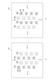
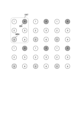
- FIG. 6 shows an example of bank switching in the first embodiment.
- “a” shows an example in which the first bank BK1 is used for distance measurement and the second bank BK2 is used for interference detection when there is no interference light LIF.
- “b” shows an example in which the first bank BK1 is used for interference detection and the second bank BK2 is used for distance measurement when there is interference light LIF.
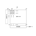
- a plurality of macro pixels PIX are provided in each of the first bank BK1 and the second bank BK2.
- the reflected light LRF is incident on each macro pixel PIX of the first bank BK1, and the reflected light LRF is not incident on each macro pixel PIX of the second bank BK2.
- the light detection unit 123 can generate a histogram HRS1 for the first bank BK1 according to the frequency of reception of the reflected light LRF. As neither the reflected light LRF nor the interference light LIF is incident on the second bank BK2, no histogram is generated.
- the light detection unit 123 can generate a histogram HSI for the first bank BK1 according to the frequency of receiving the interference light LIF.
- the light detection unit 123 can also generate a histogram HRS2 for the second bank BK2 according to the frequency of receiving the reflected light LRF and the interference light LIF.
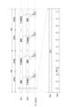
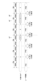
- FIG. 7 is a timing chart showing the distance measurement operation and interference detection operation in the first embodiment.
- each frame FM is divided into two subframes SFM1 and SFM2.
- laser elements are provided corresponding to the first bank BK1 and the second bank BK2.
- distance measurement is performed in the first bank BK1
- interference detection is performed in the second bank BK2.
- distance measurement is performed in the second bank BK2.
- the laser element is turned on for distance measurement, and the laser element is turned off for interference detection.
- the light detection unit 123 can set the emission interval of the laser element to PRI1.
- the light detection unit 123 detects interference, it can change the emission interval of the laser element from PRI1 to PRI2, thereby reducing interference noise.
- FIG. 8 is a diagram showing the process of generating distance measurement data and interference detection data in the first embodiment.
- a shows an example in which the first bank BK1 is used for distance measurement and the second bank BK2 is used for interference detection when there is no interference light LIF.
- b shows an example in which the first bank BK1 is used for interference detection and the second bank BK2 is used for distance measurement when there is interference light LIF.
- the TDC 133 is provided with TDCs 133-1 and 133-2 corresponding to the first bank BK1 and the second bank BK2, respectively.
- the histogram generator 134 is provided with histogram generators 134-1 and 134-2 corresponding to the first bank BK1 and the second bank BK2, respectively.
- Each macro pixel PIX is provided with a plurality of pixels 160. In each macro pixel PIX, the pixels 160 may be arranged in a 2x2 array.
- the TDC 133-1 calculates the time difference between the emission timing of the distance measurement light LML corresponding to that reflected light LRF and the reception timing of that reflected light LRF. Then, the histogram generation unit 134-1 generates a histogram HRS1 according to the reception frequency of the reflected light LRF based on the calculation result in the TDC 133-1.
- the TDC 133-1 calculates the time difference between the emission timing of the distance measurement light LML corresponding to the second bank BK2 and the reception timing of the interference light LIF. Then, the histogram generation unit 134-1 generates a histogram HRI according to the reception frequency of the interference light LIF based on the calculation result in the TDC 133-1.
- the TDC 133-2 calculates the time difference between the emission timing of the distance measurement light LML corresponding to the reflected light LRF and the reception timing of each of the reflected light LRF and the interference light LIF. Then, the histogram generation unit 134-2 generates a histogram HRS2 according to the reception frequency of each of the reflected light LRF and the interference light LIF based on the calculation results in the TDC 133-2.
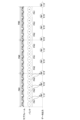
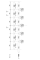
- FIG. 9 is a timing chart showing an example of data output associated with distance measurement and interference detection in the first embodiment.
- the bank selection signal BSL specifies the bank to be used for distance measurement. For example, when the first bank BK1 is used for distance measurement, the first bank BK1 is specified by the bank selection signal BSL, and when the second bank BK2 is used for distance measurement, the second bank BK2 is specified by the bank selection signal BSL.
- the bank not specified by the bank selection signal BSL is used for interference detection.
- a light emission trigger TRG is output from the light detection unit 123 to the light emission unit 112 at the time interval specified by PRI.
- the distance measurement data and interference detection data detected exclusively in the first bank BK1 and the second bank BK2, respectively, are output alternately for each subframe SFM1 and SFM2.
- FIG. 10 shows an example of an illumination pattern when switching banks in the first embodiment.
- “a” shows an example of an illumination pattern when the first bank BK1 is used for distance measurement.
- “b” shows an example of an illumination pattern when the second bank BK2 is used for distance measurement.
- an emission pattern of the distance measurement light LML is formed on the object 101 corresponding to the light receiving position of the first bank BK1.
- a non-emission pattern NML is formed on the object 101 corresponding to the light receiving position of the second bank BK2.
- This non-emission pattern NML may include interference light LIF.
- an emission pattern of the distance measurement light LML is formed on the object 101 corresponding to the light receiving position of the second bank BK2.
- a non-emission pattern NML is formed on the object 101 corresponding to the light receiving position of the first bank BK1.
- This non-emission pattern NML may include interference light LIF.
- FIG. 11 shows an example of a light receiving pattern when switching banks in the first embodiment.
- “a” shows an example of a light receiving pattern when the first bank BK1 is used for distance measurement.
- “b” shows an example of a light receiving pattern when the second bank BK2 is used for distance measurement.
- the pixel array section 131 is provided with a first bank BK1 and a second bank BK2.
- the first bank BK1 and the second bank BK2 are each provided with a plurality of macropixels PIX.
- the reflected light LRF is incident on each macropixel PIX of the first bank BK1, and the reflected light LRF is not incident on each macropixel PIX of the second bank BK2.
- the second bank BK2 when the second bank BK2 is used for distance measurement, the reflected light LRF is incident on each macropixel PIX of the second bank BK2, and the reflected light LRF is not incident on each macropixel PIX of the first bank BK1.
- FIG. 12 is a flowchart showing the interference detection process according to the first embodiment.
- control unit 136 detects the peak of the histogram acquired during the interference detection period (S101).
- the interference detection period can be set, for example, alternately for each of the subframes SFM1 and SFM2 for the first bank BK1 and the second bank BK2.
- control unit 136 determines whether or not there is a peak in the histogram acquired during the interference detection period (S102). If there is a peak in the histogram acquired during the interference detection period, the control unit 136 issues an interference flag (S103).
- the control unit 136 determines whether the interference evaluation index is equal to or greater than the threshold (S104). If the interference evaluation index is equal to or greater than the threshold, the control unit 136 issues an interference flag (S103). On the other hand, if the interference evaluation index is smaller than the threshold, the control unit 136 determines that there is no interference (S105).
- the interference evaluation index may be the signal-to-noise ratio, the ratio of the standard deviation of the interference noise to the average value, or the maximum count value of each bin of the histogram.
- the bank performing ranging and the bank performing interference detection are switched for each subframe SFM1, SFM2, and ranging based on the reflected light LRF and interference detection based on the interference light LIF are performed simultaneously.
- This makes it possible to perform interference detection even during ranging, preventing missed interference detection periods.
- This makes it possible to perform ranging while reducing the effects of various types of interference light, such as sudden interference light, persistent interference light, and intentional interference light, and thus improves ranging accuracy.
- the timing of light emission can be separated between the bank used for distance measurement and the bank used for interference detection, making it possible to suppress the peak current required for laser emission.
- Second embodiment In the first embodiment described above, the bank performing distance measurement and the bank performing interference detection were switched for each subframe SFM1, SFM2, and distance measurement based on the reflected light LRF and interference detection based on the interference light LIF were performed simultaneously. In this second embodiment, multiple banks performing distance measurement and multiple banks performing interference detection are provided, and the bank performing distance measurement and the bank performing interference detection are switched individually.
- FIG. 13 is a diagram showing an example of bank switching in the second embodiment. The figure shows an example in which six banks are provided in the pixel array section 131.
- the pixel array section 131 is provided with banks BK1 to BK6.
- the banks BK1 to BK6 may be arranged in a matrix in the row and column directions, with a 2x3 array as the unit UNT.
- Banks BK1 to BK6 can be paired with one bank performing ranging and the other performing interference detection, and these pairs can perform interleaved operations.
- banks BK1 and BK2 may be paired
- banks BK3 and BK4 may be paired
- banks BK5 and BK6 may be paired.
- banks BK3 and BK4 when bank BK3 is used for ranging, bank BK4 may be used for interference detection, and when bank BK3 is used for interference detection, bank BK4 may be used for ranging.
- the ranging banks MBK and the interference detection banks IBK are selected every other bank in the row direction and every third bank in the column direction.
- adjacent banks may be paired, or, to reduce the risk of crosstalk, banks far from each other may be paired.
- FIG. 14 is a timing chart showing the distance measurement operation and interference detection operation in the second embodiment.
- the frame FM can be divided into six subframes SFM1 to SFM6.
- one bank of distance measurement bank MBK and one bank of interference detection bank IBK can be assigned to each of the subframes SFM1 to SFM6.
- bank BK1 can be used for distance measurement
- bank BK2 can be used for interference detection
- banks BK3 to BK6 can be paused.
- bank BK1 can be used for interference detection
- bank BK2 can be used for distance measurement
- banks BK3 to BK6 can be paused.
- bank BK3 can be used for distance measurement
- bank BK4 can be used for interference detection
- banks BK1, BK2, BK5, and BK6 can be paused.
- bank BK3 can be used for interference detection
- bank BK4 can be used for distance measurement
- banks BK1, BK2, BK5, and BK6 can be paused.
- bank BK5 can be used for distance measurement
- bank BK6 can be used for interference detection
- banks BK1 to BK4 can be paused.
- bank BK5 can be used for interference detection
- bank BK6 can be used for distance measurement
- banks BK1 to BK4 can be paused.
- multiple banks for performing distance measurement and multiple banks for performing interference detection are provided, and the distance measurement bank MBK and the interference detection bank IBK are switched between. This makes it possible to simultaneously perform distance measurement and interference detection while operating some of the banks for each of the subframes SFM1 to SFM6, thereby achieving low power consumption.
- the load on generating histograms for each of the subframes SFM1 to SFM6 can be reduced, making it possible to reduce the circuit area and reducing crosstalk.
- the probability of interference times overlapping can be reduced, making it possible to suppress interference.
- the bank for performing distance measurement and the bank for performing interference detection are switched for each subframe SFM1, SFM2, and distance measurement based on the reflected light LRF and interference detection based on the interference light LIF are performed simultaneously.
- this third embodiment based on a histogram obtained by interference detection of a certain subframe, noise is removed from a histogram for distance measurement of another subframe.
- FIG. 15 is a timing chart showing the distance measurement operation and interference detection operation in the third embodiment.
- bank BK1 is used for distance measurement in subframe SFM1 and for interference detection in subframe SFM2.
- histogram HSR is generated based on distance measurement in bank BK1
- histogram HSI is generated based on interference detection in bank BK1.
- histogram HSI is added to histogram HSR.
- control unit 136 subtracts histogram HSI added to histogram HSR in subframe SFM1 based on histogram HSI in subframe SFM2.
- FIG. 16 is a block diagram showing an example of the configuration of a histogram calculation unit according to the third embodiment.
- the control unit 136 includes a histogram calculation unit 180.
- the histogram calculation unit 180 includes a first bank noise removal unit 181 and a second bank noise removal unit 182.
- Histogram data HIS11 based on the light reception of bank BK1 used for distance measurement in subframe SFM1 is input to the first bank noise removal unit 181.
- Histogram data HIS12 based on the light reception of bank BK1 used for interference detection in subframe SFM2 is input to the first bank noise removal unit 181.
- the first bank noise removal unit 181 generates and outputs histogram data HIS1 by subtracting histogram data HIS12 from the histogram data HIS11.
- the second bank noise removal unit 182 receives histogram data HIS21 based on the light reception of bank BK2 used for interference detection in subframe SFM1.
- the second bank noise removal unit 182 also receives histogram data HIS22 based on the light reception of bank BK2 used for distance measurement in subframe SFM2.
- the second bank noise removal unit 182 generates and outputs histogram data HIS2 by subtracting histogram data HIS21 from histogram data HIS22.
- the histogram calculation unit 180 can enable noise removal in each bank BK1, BK2 based on the noise removal enable signal ENB.
- noise is removed from a histogram for ranging in one subframe based on a histogram acquired by interference detection in another subframe.
- This makes it possible to remove noise including interference data from the ranging data measured for each of the subframes SFM1 and SFM2, making it possible to improve ranging accuracy while suppressing an increase in the time interval for ranging.
- noise is removed from a histogram for distance measurement of a certain subframe based on a histogram acquired by interference detection of another subframe.
- the PRI of the distance measurement light LML is randomly changed regardless of the presence or absence of the interference light LIF, thereby reducing the influence of the interference light LIF.
- FIG. 17 is a timing chart showing an example of a method for changing the laser interval in the fourth embodiment.
- each bank is used alternately for ranging and interference detection for each subframe SFM1, SFM2.
- the interference flag is turned on.
- the control unit 136 randomly changes the PRI of the ranging light LML for each frame FM, regardless of whether the interference flag is on or off.
- the control unit 136 detects interference in a certain frame FM, it may notify that the reliability of the ranging data for that frame FM is low.
- the PRI of the distance measurement light LML is changed randomly for each frame FM, regardless of whether the interference flag is on or off. This makes it possible to reduce the influence of the interference light LIF without performing a process of subtracting interference data from distance measurement data.
- a plurality of banks for performing distance measurement and a plurality of banks for performing interference detection are provided, and the banks for performing distance measurement and the banks for performing interference detection are switched between each other.
- a plurality of banks for performing distance measurement and a plurality of banks for performing interference detection are provided, and the banks for performing distance measurement and the banks for performing interference detection are switched between each other randomly.
- FIG. 18 is a timing chart showing an example of a bank switching method according to the fifth embodiment. In this figure, an example is shown in which six banks are provided in the pixel array section 131.
- the pixel array unit 131 is provided with banks BK1 to BK6.
- Banks BK1 to BK6 can be paired with one bank performing distance measurement and the other bank performing interference detection, and interleaved operation can be performed between these pairs.
- banks BK1 and BK2 can be pair PA1
- banks BK3 and BK4 can be pair PA2
- banks BK5 and BK6 can be pair PA3.
- the control unit 136 can randomly change the transition order of pairs PA1 to PA3 for each frame FM1 to FM3.
- control unit 136 can transition each pair from PA1 to PA3 in the transition order PA1 ⁇ PA3 ⁇ PA2. Also, in frame FM2, the control unit 136 can transition each pair from PA1 to PA3 in the transition order PA2 ⁇ PA1 ⁇ PA3. Also, in frame FM3, the control unit 136 can transition each pair from PA1 to PA3 in the transition order PA2 ⁇ PA3 ⁇ PA1.
- FIG. 19 is a diagram showing a first example of a bank switching method according to the fifth embodiment. Note that in the figure, a shows an example without random transitions, and b shows an example with random transitions.
- a bank transition table 191 is provided to randomly transition each pair PA1 to PA3.
- the bank transition table 191 is set to no random transition.
- the bank transition table 191 assigns a bank index BIX to the pair of subframes for each frame FM1 to FM3.
- bank indexes BIX are randomly assigned to pairs of subframes SFM1 to SFM6.
- bank indexes BIX can be set so that they do not overlap between pairs of subframes SFM1 to SFM6.
- the bank assign table 192 is set based on the bank index BIX specified in the bank transition table 191.
- the bank numbers of the odd-numbered subframes and the bank numbers of the even-numbered subframes are set for each bank index BIX. Then, according to the bank index BIX specified in the bank transition table 191, a transition is made to the bank with the bank number specified in the bank assign table 192.
- FIG. 20 is a block diagram showing a first example of a bank switching unit according to the fifth embodiment.
- control unit 136 includes a random number generator 190, a bank transition table 191, and a bank assignment table 192.
- the bank transition table 191 and the bank assignment table 192 may include registers.
- the random number generator 190 generates random numbers and outputs them to the bank transition table 191.
- the bank transition table 191 outputs the bank index BIX to the bank assignment table 192 based on the random number generated by the random number generator 190. At this time, the bank transition table 191 can randomly assign the bank index BIX to pairs of subframes SFM1 to SFM6 based on the random transition enable signal EBT. The bank transition table 191 can also reset the bank index BIX to the default based on the reset signal RST.
- the bank assignment table 192 selects the bank specified by the subframe number NSF according to the bank index BIX, and outputs the selection signal BSL of that bank.
- FIG. 21 shows a second example of a bank transition table for the fifth embodiment.
- a bank transition table 196 may be provided to randomly transition between pairs PA1 to PA3.
- the transition order of pairs PA1 to PA3 is set in the bank transition table 196, and a bank transition table index TIX is assigned to each transition order of pairs PA1 to PA3.
- FIG. 22 is a timing chart showing a second example of a bank transition method according to the fifth embodiment.
- FIG. 23 is a block diagram showing a second example of a bank switching unit according to the fifth embodiment.
- control unit 136 includes a random number generator 194, a selector 195, and a bank transition table 196.
- the random number generator 194 generates a random number and outputs it to the selector 195.
- the selector 195 selects either the bank transition table index TIX1 of the previous frame or the random number output from the random number generator 194, and outputs the selection result to the bank transition table 196 as the bank transition table index TIX2 of the next frame. At this time, the selector 195 can select the random number output from the random number generator 194 based on the random transition enable signal EBT.
- the bank transition table 196 selects the transition order of pairs PA1 to PA3 based on the bank transition table index TIX2 for the next frame output from the selector 195, and outputs the selection result as a bank selection signal BSL.
- FIG. 24 is a flowchart showing the bank transition method according to the fifth embodiment.
- control unit 136 obtains the current bank transition table index TIX (S201).
- control unit 136 determines whether bank random transition is enabled based on the random transition enable signal EBT (S202). If bank random transition is enabled, the control unit 136 randomly generates a bank transition table index TIX (S203).
- control unit 136 operates the banks in the transition order indicated by the bank transition table index TIX (S204). On the other hand, if bank random transition is not enabled, the control unit 136 proceeds to S204 without changing the bank transition table index TIX (S205).
- multiple banks for performing ranging and multiple banks for performing interference detection are provided, and the bank for performing ranging and the bank for performing interference detection are switched randomly. This makes it possible to perform ranging and interference detection simultaneously while operating some of the banks for each of the subframes SFM1 to SFM6, thereby achieving low power consumption.
- a plurality of banks are provided for performing distance measurement and a plurality of banks are provided for performing interference detection, and the bank for performing distance measurement and the bank for performing interference detection are switched randomly.
- a plurality of banks are provided for performing distance measurement and a plurality of banks are provided for performing interference detection, and the bank for performing distance measurement and the bank for performing interference detection can be selected.
- FIG. 25 is a diagram showing an example of a bank selection method according to the sixth embodiment. Note that in the figure, a shows an example of full-surface ranging or full-surface sparse ranging, and b shows an example of ROI (Region Of Interest) ranging.
- ROI Region Of Interest
- the pixel array unit 131 is provided with banks BK1 to BK16. Each bank BK1 to BK16 may be arranged discretely over the entire surface of the pixel array unit 131.
- the control unit 136 can perform full surface ranging simultaneously with interference detection by transitioning banks BK1 to BK16. Also, the control unit 136 can perform full surface sparse ranging simultaneously with interference detection by transitioning banks BK1 to BK4, for example.
- the control unit 136 may switch between full surface ranging and full surface sparse ranging depending on interference detection. At this time, the control unit 136 may speed up interference detection based on full surface sparse ranging to detect the presence or absence of interference, or may improve the resolution based on full surface ranging if there is no interference.
- the pixel array section 131 is provided with banks BK1 to BK32.
- the pixel array section 131 can be divided into a plurality of blocks.
- the pixel array section 131 may be divided into four blocks.
- the first block 300 may have banks BK1 to BK8, the second block may have banks BK9 to BK16, the third block may have banks BK17 to BK24, and the fourth block may have banks BK25 to BK32.
- the control section 136 may specify, for example, the first block 300 as the ROI. In this case, by transitioning banks BK1 to BK8 of the first block 300 specified as the ROI, interference detection and ROI distance measurement can be performed at the same time.
- FIG. 26 is a timing chart showing an example of the transition of the interference flag referenced in bank selection in the sixth embodiment
- FIG. 27 is a diagram showing a bank selection method based on the transition of the interference flag in the sixth embodiment.
- the control unit 136 can change the number of banks used alternately for ranging and interference detection for each of frames FM1 to FM3.
- the control unit 136 can set the number of subframes into which each of frames FM1 to FM3 is divided according to the number of banks used alternately for ranging and interference detection.
- the control unit 136 may change the number of banks used alternately for ranging and interference detection according to the presence or absence of interference.
- the pixel array section 131 can be divided into two banks, BK1 and BK2, and distance measurement and interference detection for the entire surface can be completed in two subframes SFM1 and SFM2. If it is determined that there is no interference in frame FM1, then in the next frame FM2, banks BK1 to BK6 can be used to operate some of the banks while distance measurement and interference detection are performed simultaneously, thereby achieving low power consumption. At this time, subframes SFM1 to SFM6 are provided in frame FM2.
- the pixel array section 131 is divided into two banks, BK1 and BK2, and distance measurement and interference detection are performed simultaneously, allowing for rapid confirmation across the entire surface as to whether the interference reduction operation has worked effectively.
- multiple banks for performing distance measurement and multiple banks for performing interference detection are provided, and the bank for performing distance measurement and the bank for performing interference detection can be selected. This makes it possible to speed up interference detection and reduce power consumption depending on whether interference is present.
- the PRI of the distance measurement light LML is randomly changed regardless of the presence or absence of the interference light LIF to reduce the influence of the interference light LIF.
- the PRI of the distance measurement light LML is randomly changed without performing interference detection to reduce the influence of the interference light LIF.
- FIG. 28 is a timing chart showing the distance measurement operation according to the seventh embodiment.
- a bank for distance measurement is provided in pixel array section 131.
- Pixel array section 131 may or may not have a bank for interference detection. If pixel array section 131 has a bank for interference detection, the interference detection function is turned off.
- Each bank is used for distance measurement for each frame FM.
- the laser is turned on. At this time, even if interference light LIF is incident, interference detection is not performed.
- the control unit 136 randomly changes the PRI of the distance measurement light LML for each frame FM without performing interference detection.
- the PRI of the distance measurement light LML may be changed randomly according to a random pattern or a fixed pattern. In the all-bank transition, the interference detection function may be turned off, and a high frame rate may be selected.
- FIG. 29 is an example of a flowchart showing the distance measurement operation according to the seventh embodiment.
- the pixel array unit 131 is provided with a bank for distance measurement and a bank for interference detection, and an example is shown in which the interference detection function is turned on/off based on the bank transition mode.
- the number of banks to be transitioned is full bank transition mode>first partial bank transition mode>second partial bank transition mode.
- control unit 136 determines whether to select the all-bank transition mode (S301). If the control unit 136 selects the all-bank transition mode, it turns off the interference detection function (S302).
- control unit 136 determines whether to select the high frame rate (S303). If the control unit 136 selects the high frame rate, it selects the first frame rate (S304).
- control unit 136 determines not to select the all-bank transition mode (S301), it determines whether to select the first partial transition mode (S305). If the control unit 136 selects the first partial transition mode, it determines whether to turn on the interference detection function (S306). If the control unit 136 determines to turn on the interference detection function, it turns on the interference detection function (S307), and if it determines not to turn on the interference detection function, it turns off the interference detection function (S308).
- control unit 136 determines whether to select the high frame rate (S309). If the control unit 136 selects the high frame rate, it selects the second frame rate (S310).
- control unit 136 determines not to select the first partial transition mode (S305), it determines whether to select the second partial transition mode (S311). If the control unit 136 selects the second partial transition mode, it determines whether to turn on the interference detection function (S312). If the control unit 136 determines to turn on the interference detection function, it turns on the interference detection function (S313), and if it determines not to turn on the interference detection function, it turns off the interference detection function (S314). Next, the control unit 136 selects a third frame rate (S315).
- the PRI of the distance measurement light LML is changed randomly without performing interference detection. This makes it possible to interrupt the influence of the interference light LIF while eliminating the load on the interference detection, and to speed up full-surface distance measurement while suppressing a decrease in distance measurement accuracy.
- the bank for distance measurement and the bank for interference detection are switched for each subframe SFM1, SFM2, and distance measurement based on the reflected light LRF and interference detection based on the interference light LIF are performed simultaneously.
- interference detection is performed based on light reception at non-emission timing provided between light emission timings based on light emission triggers.
- FIG. 30 is a block diagram showing an example of the configuration of an imaging device according to the eighth embodiment.
- the imaging device 500 captures a distance image based on ToF.
- the imaging device 500 provides non-light emission timing between light emission timings based on the light emission trigger TRG in order to perform interference detection.
- the light emission timings and non-light emission timings may be set alternately. There may be one or more light emission timings between the non-light emission timings.
- the imaging device 500 can control the setting of the light emission period including the light emission timings and the non-light emission period including the non-light emission timings.
- the light emission trigger TRG specifies the light emission timing of the light emitting unit that emits distance measurement light. Then, the imaging device 500 performs interference detection based on the detection result of the light received at the non-light emission timings.
- the imaging device 500 may notify the outside of the detection result of the interference light that interferes with the distance measurement light.
- the imaging device 500 may also calculate distance measurement data based on the light reception in response to the light emission at the light emission timings, and correct the distance measurement data based on the detection result of the interference light detected based on the non-light emission timings.
- the imaging device 500 includes a pixel array section 551, a sampling circuit 552, a light receiving control section 553, an overall control section 554, a light emission control section 555, a timing control section 556, and a distance measurement processing section 560.
- the imaging device 500 also includes an output interface 570, a PLL (Phase Locked Loop) circuit 581, and a clock generation section 582. These circuits may be arranged on a single semiconductor substrate or on a laminated substrate.
- PLL Phase Locked Loop
- pixels 557 are arranged in a matrix shape in the row and column directions.
- a light receiving section is provided in the pixel 557.
- the light receiving section receives reflected light that is the distance measurement light emitted from the light emitting section.
- the light receiving section may be a SPAD.
- a circuit section such as a quench resistor and a recharge circuit may be provided for each pixel 557.
- the sampling circuit 552 samples the light receiving signal at each pixel 557 based on the light emission timing, and samples the light receiving signal at each pixel 557 based on the non-light emission timing. Sampling may be performed multiple times for each light emission timing and non-light emission timing. Multiple light emission timings and non-light emission timings may be set within one frame. The sampling circuit 552 may select the rows to sample in sequence.
- the light receiving control unit 553 controls the operation of the light receiving unit in each pixel 557. At this time, the light receiving control unit 553 may also control the quenching and recharging of the SPAD.
- the overall control unit 554 controls the light receiving control unit 553, the light emission control unit 555, the timing control unit 556, and the distance measurement processing unit 560. At this time, the overall control unit 554 can cause the light receiving control unit 553, the light emission control unit 555, the timing control unit 556, and the distance measurement processing unit 560 to operate in coordination. The overall control unit 554 can notify the timing control unit 556 of the light emission timing.
- the overall control unit 554 may perform communication control with an externally connected host. Communication with the outside may be by a method using I2C (Inter-Integrated Circuit) or a method using SPI (Serial Peripheral Interface).
- the light emission control unit 555 controls the light emission of the light emitting unit that emits distance measurement light. At this time, the light emission control unit 555 can instruct the selection of a trigger for generating only a histogram and a light emission trigger TRG.
- the timing control unit 556 under the control of the light emission control unit 555, outputs a light emission trigger TRG to the light emission histogram generation unit 561 and outputs a non-light emission trigger NRG to the non-light emission histogram generation unit 562.
- the timing control unit 556 also outputs a light emission trigger TRG to the light emission unit that emits distance measurement light.
- the non-light emission trigger NRG can specify the timing for generating a histogram when no light is emitted.
- the distance measurement processing unit 560 can also generate a histogram by adding up the number of responses of the SPAD during non-light emission timing between light emission timings based on the light emission trigger TRG, and detect interference light from the histogram. The distance measurement processing unit 560 can then correct the distance measurement data based on the detection result of the interference light detected based on the non-light emission timing.
- the distance measurement processing unit 560 includes an emission histogram generating unit 561, a non-emission histogram generating unit 562, an interference correction unit 563, and a distance calculation unit 564.
- the light emission histogram generating unit 561 generates a histogram by adding up the number of SPAD responses at each sampling time of light reception in response to light emission based on the light emission trigger TRG.
- the light emission histogram generating unit 561 generates a histogram in slot units.
- a slot unit is the unit for generating a histogram. Multiple slots can be provided within one frame.
- the non-light emitting histogram generator 562 generates a histogram by adding up the number of SPAD responses for each sampling time of light reception based on the non-light emitting trigger NRG.
- the light emitting histogram generator 561 generates a histogram on a slot-by-slot basis.
- the interference correction unit 563 corrects the histogram generated by the emission histogram generation unit 561 based on the histogram generated by the non-emission histogram generation unit 562. At this time, the interference correction unit 563 may subtract the histogram generated by the non-emission histogram generation unit 562 from the histogram generated by the emission histogram generation unit 561 to generate a histogram for the reflected light from which the interference light has been removed.
- the distance calculation unit 564 calculates the distance to the subject based on the histogram corrected by the interference correction unit 563.
- the distance calculation unit 564 may output ranging data indicating the distance to the subject to the output interface 570.
- the distance calculation unit 564 may include an FIR (Finite Impulse Response) filter.
- the distance calculation unit 564 may perform echo determination and histogram peaks to calculate the distance to the subject.
- the clock generation unit 582 generates an internal clock CKI based on the external clock CKO input via the PLL circuit 581.
- FIG. 31 shows a method for generating a histogram based on an emission trigger and a non-emission trigger in the eighth embodiment.
- the sampling start timing based on the light emission trigger TRG and the sampling start timing based on the non-light emission trigger NRG are set alternately.
- the sampling start interval TIV can be set between several hundred nsec and several ⁇ sec.
- the light emission histogram generating unit 561 generates histograms 601-1 and 601-2 by adding up the number of SPAD responses for each sampling time based on each light emission trigger TRG.
- the light emission histogram generating unit 561 then generates histogram 601 by adding up histograms 601-1 and 601-2 based on multiple light emission triggers TRG.
- the non-light emitting histogram generating unit 562 generates histograms 602-1 and 602-2 by adding up the number of SPAD responses for each sampling time based on each non-light emitting trigger NRG.
- the non-light emitting histogram generating unit 562 then generates histogram 602 by adding up histograms 602-1 and 602-2 based on multiple non-light emitting triggers NRG.
- FIG. 32 shows an interference correction method according to the eighth embodiment.
- the light emission histogram generation unit 561 generates a histogram 600 based on the light emission trigger TRG.
- the histogram 600 is generated by adding a histogram 602 of the interference light to a histogram 601 of the reflected light when there is no interference light.
- the non-light emission histogram generation unit 562 generates a histogram 602 based on the non-light emission trigger NRG.
- the histogram 602 is generated by adding up the number of reactions of the SPAD at each sampling time of receiving the interference light.
- the interference correction unit 563 subtracts the histogram 601 generated by the non-emission histogram generation unit 562 from the histogram 600 generated by the emission histogram generation unit 561. This allows the interference correction unit 563 to extract the histogram 601 for the reflected light from which the interference light has been removed, from the histogram 600 generated by the emission histogram generation unit 561.
- interference detection is performed based on the non-emission timing provided between the emission timings based on the emission trigger TRG. This makes it possible to shorten the sampling interval of the received light signal used for interference detection while avoiding overlap with the emission timing. This makes it possible to perform distance measurement while reducing the effects of various types of interference light, such as sudden interference light, persistent interference light, and intentional interference light, thereby improving distance measurement accuracy.
- interference detection is performed based on the non-light emission timing provided between the light emission timings based on the light emission trigger TRG.
- a plurality of light emission timings based on the light emission trigger TRG are provided between the non-light emission timings.
- FIG. 33 is a timing chart showing a sampling method based on a light emission trigger and a non-light emission trigger in the ninth embodiment.
- multiple light emitting triggers TRGs are provided between non-light emitting triggers NRGs.
- the number of light emitting triggers TRGs provided between non-light emitting triggers NRGs may be two or more.
- the number of light emitting triggers TRGs provided between non-light emitting triggers NRGs may vary. Multiple non-light emitting triggers NRGs may be provided between light emitting triggers TRGs.
- the interference correction unit 563 may use a histogram based on a non-light emission trigger NRG that is two or more triggers before or after the current light emission trigger TRG in order to remove the effects of interference light from the distance measurement data.
- multiple light emission timings based on the light emission trigger TRG are provided between non-light emission timings. This makes it possible to increase the number of samplings of the light reception signal based on the light emission trigger TRG, and to reduce the effects of various types of interference light, such as sudden interference light, persistent interference light, and intentional interference light, while suppressing a decrease in distance measurement accuracy.
- Tenth embodiment> In the above-described ninth embodiment, a plurality of light emission timings based on the light emission trigger TRG are provided between non-light emission timings. In the tenth embodiment, non-light emission timings are provided randomly between light emission timings based on the light emission trigger TRG.
- FIG. 34 is a timing chart showing a sampling method based on a light emission trigger and a non-light emission trigger in the tenth embodiment.
- non-light emitting triggers NRG are placed randomly between light emitting triggers TRG. Multiple non-light emitting triggers may also be placed randomly between light emitting triggers TRG.
- the interference correction unit 563 may use a histogram based on the closest non-emission trigger NRG to the current emission trigger TRG in order to remove the effects of interference light from the distance measurement data.
- non-emission timings are set randomly between emission timings based on the emission trigger TRG. This makes it difficult to predict the current emission timing from past emission timings, and strengthens security against attacks that use intentional interference light, etc.
- interference detection is performed based on the non-light emission timing provided between the light emission timings based on the light emission trigger TRG.
- a series of light emission triggers and a series of non-light emission triggers are generated based on a histogram generation unit.
- FIG. 35 is a timing chart showing a sampling method based on a light emission trigger and a non-light emission trigger in the eleventh embodiment.
- each histogram generation unit light emission triggers TRG and non-light emission triggers NRG are provided alternately.
- non-light emission triggers NRG may be provided randomly between light emission triggers TRG.
- a histogram 600 for distance measurement that includes interference and a histogram 602 for interference detection are generated for each histogram generation unit.
- the sampling accuracy of the signal used for interference detection may be lower than the sampling accuracy of the signal used for distance measurement.
- the resolution of the interference detection image may be lower than the resolution of the distance measurement image.
- the light emitting trigger TRG and the non-light emitting trigger NRG will not be set strictly at 4:1, and the non-light emitting trigger NRG may increase or decrease several times more than the probability of 20%.
- the imaging device 500 may record the number of accumulations of the histogram and reflect that number of accumulations in the histogram subtraction process for removing the interfering light.
- the imaging device 500 may notify the number of accumulations to the outside together with the histogram data.
- the imaging device 500 may add the number of accumulations of the histogram to the EBD (Embedded Data) of the histogram data.
- a series of light emission triggers and non-light emission triggers is generated based on the histogram generation unit. This allows the number of histogram accumulations to be reflected in the histogram subtraction process for removing interference light while also dealing with randomization of the non-light emission triggers NRG. This makes it possible to improve distance measurement accuracy while strengthening security against attacks that intentionally use interference light.
- Twelfth embodiment In the eleventh embodiment described above, the light emission triggers TRG and the non-light emission triggers NRG are alternately provided in each histogram generation unit. In the twelfth embodiment, a series of light emission triggers TRG and a series of non-light emission triggers NRG are alternately provided for each histogram generation unit.
- FIG. 36 is a timing chart showing a sampling method based on a light emission trigger and a non-light emission trigger in the 12th embodiment.
- a series of light emission triggers TRG and a series of non-light emission triggers NRG are provided alternately for each histogram generation unit.
- a histogram 600 for distance measurement mixed with interference and a histogram 602 for interference detection are generated alternately for each histogram generation unit. Therefore, the imaging device 500 only needs to alternately store the histogram 600 for distance measurement mixed with interference and the histogram 602 for interference detection, and the two types of histograms 600 and 602 can be stored in the same memory in a time-division manner. This makes it possible to reduce the storage capacity required to store the two types of histograms 600 and 602, and to miniaturize the imaging device 500.
- the distance measurement data and the interference detection data may be stored as histogram data, or may be compressed and stored as information that can reproduce waveforms such as the peak position and half-width of the histogram or information around the peak.
- a series of light emission triggers TRG and a series of non-light emission triggers NRG are provided for each histogram generation unit. This makes it possible to generate a distance measurement histogram 600 containing interference and a histogram for interference detection 602 for each histogram generation unit, and the two types of histograms 600, 602 can be stored in the same memory in a time-division manner.
- interference detection is performed based on the non-light emission timing provided between the light emission timings based on the light emission trigger TRG.
- the measurable distance is divided to generate a histogram based on the light emission trigger TRG and a histogram based on the non-light emission trigger NRG.
- FIG. 37 shows an example of a method for sampling interference data according to the thirteenth embodiment.
- the imaging device 500 is assumed to be capable of measuring distances up to 100 m without interference detection. In this case, when performing distance measurement with interference detection, the imaging device 500 switches to measuring distances up to 50 m.
- histogram 701 is created for distance measurement up to 100 m without interference
- histogram 702 is created for interference detection up to 100 m with interference.
- it is sufficient to have memory capacity to store histogram 701.
- memory capacity is required to store histograms 701 and 702, and it is necessary to increase the memory capacity to store histogram 702.
- the imaging device 500 switches to distance measurement up to 50 m.
- a histogram is generated in which histograms 701 and 702 up to 50 m are added together.
- a histogram 702 is generated in which histogram 701 up to 50 m is not added. For this reason, by subtracting histogram 702 up to 50 m in c in the same figure from the histogram in b in the same figure in which histograms 701 and 702 up to 50 m are added together, it is possible to generate histogram 701 up to 50 m from which interference has been removed.
- the presence or absence of interference may be determined based on a peak at a position farther than 50 m.
- the reflected light of the distance measurement light is attenuated more as the distance increases, so no peak occurs at a position far away.
- a peak may occur with interference light even at a long distance.
- the histogram 702 of the interference light a peak 703 may occur even at a position farther than 50 m.
- the presence or absence of interference can be determined by determining whether the peak 703 of the histogram 702 is added to the histogram 701 up to 100 m at a position farther than 50 m.
- interference detection may be performed between multiple frames at a position far from the subject.
- the measurable distance is divided, and a histogram based on the light emission trigger TRG and a histogram based on the non-light emission trigger NRG are generated. This makes it possible to switch between distance measurement with interference detection and distance measurement without interference detection depending on the distance to the subject, and makes it possible to perform distance measurement with interference detection based on the memory capacity corresponding to distance measurement without interference detection.
- interference detection is performed based on the non-light emission timing provided between the light emission timings based on the light emission trigger TRG.
- the sampling accuracy based on the non-light emission trigger NRG is set lower than the sampling accuracy based on the light emission trigger TRG.
- FIG. 38 shows an example of a method for sampling interference data according to the fourteenth embodiment.
- the imaging device 500 is capable of measuring distances up to 100 m, for example.
- the imaging device 500 generates histogram 801 by adding sampling data based on 100 m and 100 light emission triggers TRG with a sampling accuracy of 5 cm, for example.
- the imaging device 500 generates histogram 802 by adding sampling data based on 100 m and 25 non-light emission triggers NRG with a sampling accuracy of 10 cm, for example.
- the sampling accuracy of interference detection can be made lower than the sampling accuracy of distance measurement, and the storage capacity of histogram 802 can be reduced.
- the imaging device 500 may allocate, for example, 70 m of the 100 m of the storage capacity of histogram 801 to the storage capacity of histogram 802. In this case, the imaging device 500 can allocate 30 m of the 100 m of the storage capacity of histogram 801 to the storage capacity of histogram 802.
- the imaging device 500 reduces the sampling accuracy and number of additions of the histogram 802, and stores 70 m of the histogram 802 in the storage capacity of 30 m of the histogram 801. This makes it possible to perform interference detection based on timing that does not overlap with distance measurement, without increasing the storage capacity of the histogram 802.
- the sampling accuracy based on the non-light emission trigger NRG is set lower than the sampling accuracy based on the light emission trigger TRG. This makes it possible to compress the data of the interference detection histogram 602, thereby reducing the storage capacity of the interference detection histogram 602.
- interference correction is performed within the imaging device 500 based on interference detection by the imaging device 500.
- interference correction is performed outside the imaging device based on interference detection by the imaging device.
- FIG. 39 is a block diagram showing an example of the configuration of an imaging device according to the fifteenth embodiment.
- the imaging device 800 includes a distance measurement processing unit 860 instead of the distance measurement processing unit 560 of the imaging device 500 of the eighth embodiment described above.
- the rest of the configuration of the imaging device 800 is the same as the configuration of the imaging device 500 of the eighth embodiment described above.
- the distance measurement processing unit 860 includes a selector 861 and a preprocessing unit 862 instead of the interference correction unit 563 and the distance calculation unit 564 of the distance measurement processing unit 560 of the eighth embodiment described above.
- the rest of the configuration of the distance measurement processing unit 860 is the same as the configuration of the distance measurement processing unit 560 of the eighth embodiment described above.
- the selector 861 selectively outputs the output of the emission histogram generation unit 561 and the output of the non-emission histogram generation unit 562 to the pre-processing unit 862.
- the pre-processing unit 862 performs pre-processing of interference correction on the output of the emission histogram generating unit 561 and the output of the non-emission histogram generating unit 562.
- the pre-processing unit 862 may include an FIR filter.
- the pre-processing unit 862 may perform echo determination.
- the host 811 is connected to the imaging device 800.
- the host 811 processes the output of the imaging device 800.
- the host 811 includes an input interface 812 and an interference correction unit 813.
- the output of the imaging device 800 is input to the interference correction unit 813 via the input interface 812.
- the interference correction unit 813 corrects the histogram generated by the emission histogram generation unit 561 based on the histogram generated by the non-emission histogram generation unit 562.
- the interference correction unit 813 may subtract the histogram generated by the non-emission histogram generation unit 562 from the histogram generated by the emission histogram generation unit 561 to generate a histogram for the reflected light from which the interference light has been removed.
- interference correction is performed outside the imaging device 800 based on interference detection by the imaging device 800. This makes it possible to reduce the load on the imaging device 800 for interference correction.
- interference correction is performed outside the imaging device 800 based on interference detection by the imaging device 800.
- the imaging device notifies the outside of the detection result of the interference light.
- FIG. 40 is a block diagram showing an example of the configuration of an imaging device according to the 16th embodiment.
- the imaging device 850 is obtained by adding a peak detection unit 851 to the imaging device 500 of the eighth embodiment described above.
- the rest of the configuration of the imaging device 850 is the same as the configuration of the imaging device 500 of the eighth embodiment described above.
- the peak detection unit 851 detects peaks in the histogram generated by the non-luminescence histogram generation unit 562, and notifies the outside of the imaging device 850 as warning information.
- the warning information may be notified to the outside via a terminal, or may be notified to the outside via the output interface 570.
- the warning information may be inserted into an EBD or the like and notified to the outside.
- the imaging device 850 notifies the outside of the detection result of the interference light. This makes it possible to externally confirm the interference during distance measurement by the imaging device 850.
- ⁇ 17. Seventeenth embodiment> In the first embodiment described above, the bank performing distance measurement and the bank performing interference detection were switched for each subframe SFM1, SFM2, and distance measurement based on the reflected light LRF and interference detection based on the interference light LIF were performed simultaneously.
- a pixel array unit in which pixels each having a light receiving element are arranged is provided on an upper chip, and a circuit unit is provided on a lower chip.
- FIG. 41 is a perspective view showing an example of a stack of a solid-state imaging device according to the seventeenth embodiment.
- the solid-state imaging device includes a pixel array section 910 and a circuit section 920.
- the pixel array section 910 can be stacked on the circuit section 920.
- the pixel array section 910 includes pixels 911.
- the pixels 911 are arranged in a matrix shape in the row and column directions.
- the pixels 911 can be provided with a light receiving section such as a SPAD, a quench resistor, a recharge circuit, a counter, a latch, and the like.
- the circuit section 920 is connected to the pixel array section 910.
- the circuit section 920 can be provided with a readout circuit 921 and a control circuit 922.
- the readout circuit 921 reads out pixel data from each pixel 911 of the pixel array section 910.
- the control circuit 922 can control the emission timing of the light emitting section and the sampling timing of the light receiving signal generated by the light receiving section. In addition, based on the sampling of the light receiving signal, a histogram showing the frequency of light receiving for each distance can be generated, and the distance to the subject can be calculated based on the histogram. At this time, the control circuit 922 can perform interference detection and correct the distance measurement data based on the interference detection data.
- the pixel array section 910 can be formed in the upper chip, and the circuit section 920 can be formed in the lower chip.
- the upper chip and the lower chip can be directly bonded.
- Hybrid bonding can be used for directly bonding the upper chip and the lower chip.
- the upper chip and the lower chip can be electrically connected based on a Cu-Cu connection.
- the material of the semiconductor substrate used for the upper chip and the lower chip can be Si, InGaAs, or InP.
- the pixel array section 910 in which the pixels 911 each having a light receiving element are arranged is provided on the upper chip, and the circuit section 920 is provided on the lower chip. This makes it possible to increase the area of the light receiving element while suppressing an increase in chip size, thereby improving sensitivity while miniaturizing the solid-state imaging device.
- the pixel array section 910 in which the pixels 911 are arranged is laminated on the circuit section 920.
- the light receiving array section in which the light receiving sections are arranged is provided on an upper chip, and the circuit array section is provided on a lower chip.
- FIG. 42 is a perspective view showing an example of a pixel array section stacked in the 18th embodiment.
- the pixel array section includes a light receiving array section 930 and a circuit array section 940.
- the light receiving array section 930 can be stacked on the circuit array section 940.
- the light receiving array section 930 includes light receiving sections 931.
- the light receiving sections 931 are arranged in a matrix shape in the row and column directions. Each light receiving section 931 can be provided with a SPAD.
- the circuit array section 940 includes circuit sections 941.
- the circuit sections 941 are arranged in a matrix shape in the row and column directions.
- a circuit section 941 can be provided for each light receiving section 931.
- Each circuit section 941 can be provided with a quench resistor, a recharge circuit, a counter, a latch, etc.
- the light receiving array section 930 in which the light receiving sections 931 are arranged is stacked on the circuit array section 940 in which the circuit sections 941 are arranged. This makes it possible to increase the area of the light receiving sections 931 while suppressing an increase in chip size, thereby improving sensitivity while miniaturizing the solid-state imaging device.
- the light receiving array section 930 in which the light receiving sections 931 are arranged is stacked on the circuit array section 940 in which the circuit sections 941 are arranged.
- the light receiving array section in which the light receiving sections, each having a plurality of light receiving elements, are arranged is provided on an upper chip, and the circuit array section is provided on a lower chip.
- FIG. 43 is a perspective view showing an example of a pixel array section stacked in the 19th embodiment.
- the pixel array section includes a light receiving array section 950 and a circuit array section 960.
- the light receiving array section 950 can be stacked on the circuit array section 960.
- the light receiving array section 950 includes a light receiving section 951.
- the light receiving sections 951 are arranged in a matrix shape in the row and column directions. Each light receiving section 951 is provided with a plurality of light receiving elements 952.
- the light receiving elements 952 may be SPADs. In each light receiving section 951, the light receiving elements 952 may be arranged in a 2x2 array or a 3x3 array.
- the circuit array section 960 includes circuit sections 961.
- the circuit sections 961 are arranged in a matrix shape in the row and column directions.
- a circuit section 961 can be provided for each light receiving section 951.
- Each circuit section 961 can be provided with a quench resistor, a recharge circuit, a counter, a latch, etc.
- a light receiving array section 950 in which light receiving sections 951 each having a plurality of light receiving elements 952 are arranged is stacked on a circuit array section 960 in which circuit sections 961 are arranged.
- the technology according to the present disclosure can be applied to various products.
- the technology according to the present disclosure may be realized as a device mounted on any type of moving body such as an automobile, an electric vehicle, a hybrid electric vehicle, a motorcycle, a bicycle, a personal mobility device, an airplane, a drone, a ship, or a robot.
- FIG. 44 is a block diagram showing a schematic configuration example of a vehicle control system, which is an example of a mobile object control system to which the technology disclosed herein can be applied.
- the vehicle control system 12000 includes a plurality of electronic control units connected via a communication network 12001.
- the vehicle control system 12000 includes a drive system control unit 12010, a body system control unit 12020, an outside vehicle information detection unit 12030, an inside vehicle information detection unit 12040, and an integrated control unit 12050.
- Also shown as functional components of the integrated control unit 12050 are a microcomputer 12051, an audio/video output unit 12052, and an in-vehicle network I/F (interface) 12053.
- the drive system control unit 12010 controls the operation of devices related to the drive system of the vehicle according to various programs.
- the drive system control unit 12010 functions as a control device for a drive force generating device for generating the drive force of the vehicle, such as an internal combustion engine or a drive motor, a drive force transmission mechanism for transmitting the drive force to the wheels, a steering mechanism for adjusting the steering angle of the vehicle, and a braking device for generating a braking force for the vehicle.
- the body system control unit 12020 controls the operation of various devices installed in the vehicle body according to various programs.
- the body system control unit 12020 functions as a control device for a keyless entry system, a smart key system, a power window device, or various lamps such as headlamps, tail lamps, brake lamps, turn signals, and fog lamps.
- radio waves or signals from various switches transmitted from a portable device that replaces a key can be input to the body system control unit 12020.
- the body system control unit 12020 accepts the input of these radio waves or signals and controls the vehicle's door lock device, power window device, lamps, etc.
- the outside-vehicle information detection unit 12030 detects information outside the vehicle equipped with the vehicle control system 12000.
- the image capturing unit 12031 is connected to the outside-vehicle information detection unit 12030.
- the outside-vehicle information detection unit 12030 causes the image capturing unit 12031 to capture images outside the vehicle and receives the captured images.
- the outside-vehicle information detection unit 12030 may perform object detection processing or distance detection processing for people, cars, obstacles, signs, or characters on the road surface based on the received images.
- the imaging unit 12031 is an optical sensor that receives light and outputs an electrical signal according to the amount of light received.
- the imaging unit 12031 can output the electrical signal as an image, or as distance measurement information.
- the light received by the imaging unit 12031 may be visible light, or may be invisible light such as infrared light.
- the in-vehicle information detection unit 12040 detects information inside the vehicle.
- a driver state detection unit 12041 that detects the state of the driver is connected.
- the driver state detection unit 12041 includes, for example, a camera that captures an image of the driver, and the in-vehicle information detection unit 12040 may calculate the driver's degree of fatigue or concentration based on the detection information input from the driver state detection unit 12041, or may determine whether the driver is dozing off.
- the microcomputer 12051 can calculate control target values for the driving force generating device, steering mechanism, or braking device based on information inside and outside the vehicle acquired by the outside vehicle information detection unit 12030 or the inside vehicle information detection unit 12040, and output control commands to the drive system control unit 12010.
- the microcomputer 12051 can perform cooperative control aimed at realizing the functions of an Advanced Driver Assistance System (ADAS), including vehicle collision avoidance or impact mitigation, following driving based on the distance between vehicles, maintaining vehicle speed, vehicle collision warning, or vehicle lane departure warning.
- ADAS Advanced Driver Assistance System
- the microcomputer 12051 can also control the driving force generating device, steering mechanism, braking device, etc. based on information about the surroundings of the vehicle acquired by the outside vehicle information detection unit 12030 or the inside vehicle information detection unit 12040, thereby performing cooperative control aimed at automatic driving, which allows the vehicle to travel autonomously without relying on the driver's operation.
- the microcomputer 12051 can also output control commands to the body system control unit 12020 based on information outside the vehicle acquired by the outside-vehicle information detection unit 12030. For example, the microcomputer 12051 can control the headlamps according to the position of a preceding vehicle or an oncoming vehicle detected by the outside-vehicle information detection unit 12030, and perform cooperative control aimed at preventing glare, such as switching high beams to low beams.
- the audio/image output unit 12052 transmits at least one output signal of audio and image to an output device capable of visually or audibly notifying the occupants of the vehicle or the outside of the vehicle of information.
- an audio speaker 12061, a display unit 12062, and an instrument panel 12063 are exemplified as output devices.
- the display unit 12062 may include, for example, at least one of an on-board display and a head-up display.
- FIG. 45 shows an example of the installation position of the imaging unit 12031.
- the imaging unit 12031 includes imaging units 12101, 12102, 12103, 12104, and 12105.
- the imaging units 12101, 12102, 12103, 12104, and 12105 are provided, for example, at the front nose, side mirrors, rear bumper, back door, and upper part of the windshield inside the vehicle cabin of the vehicle 12100.
- the imaging unit 12101 provided at the front nose and the imaging unit 12105 provided at the upper part of the windshield inside the vehicle cabin mainly acquire images of the front of the vehicle 12100.
- the imaging units 12102 and 12103 provided at the side mirrors mainly acquire images of the sides of the vehicle 12100.
- the imaging unit 12104 provided at the rear bumper or back door mainly acquires images of the rear of the vehicle 12100.
- the imaging unit 12105 provided at the upper part of the windshield inside the vehicle cabin is mainly used to detect leading vehicles, pedestrians, obstacles, traffic lights, traffic signs, lanes, etc.
- FIG. 45 shows an example of the imaging ranges of the imaging units 12101 to 12104.
- Imaging range 12111 indicates the imaging range of the imaging unit 12101 provided on the front nose
- imaging ranges 12112 and 12113 indicate the imaging ranges of the imaging units 12102 and 12103 provided on the side mirrors, respectively
- imaging range 12114 indicates the imaging range of the imaging unit 12104 provided on the rear bumper or back door.
- an overhead image of the vehicle 12100 viewed from above is obtained by superimposing the image data captured by the imaging units 12101 to 12104.
- At least one of the imaging units 12101 to 12104 may have a function of acquiring distance information.
- at least one of the imaging units 12101 to 12104 may be a stereo camera consisting of multiple imaging elements, or an imaging element having pixels for detecting phase differences.
- the microcomputer 12051 can obtain the distance to each solid object within the imaging ranges 12111 to 12114 and the change in this distance over time (relative speed with respect to the vehicle 12100) based on the distance information obtained from the imaging units 12101 to 12104, and can extract as a preceding vehicle, in particular, the closest solid object on the path of the vehicle 12100 that is traveling in approximately the same direction as the vehicle 12100 at a predetermined speed (e.g., 0 km/h or faster). Furthermore, the microcomputer 12051 can set the inter-vehicle distance that should be maintained in advance in front of the preceding vehicle, and perform automatic braking control (including follow-up stop control) and automatic acceleration control (including follow-up start control). In this way, cooperative control can be performed for the purpose of automatic driving, which runs autonomously without relying on the driver's operation.
- automatic braking control including follow-up stop control
- automatic acceleration control including follow-up start control
- the microcomputer 12051 classifies and extracts three-dimensional object data on three-dimensional objects, such as two-wheeled vehicles, ordinary vehicles, large vehicles, pedestrians, utility poles, and other three-dimensional objects, based on the distance information obtained from the imaging units 12101 to 12104, and can use the data to automatically avoid obstacles.
- the microcomputer 12051 distinguishes obstacles around the vehicle 12100 into obstacles that are visible to the driver of the vehicle 12100 and obstacles that are difficult to see.
- the microcomputer 12051 determines the collision risk, which indicates the risk of collision with each obstacle, and when the collision risk is equal to or exceeds a set value and there is a possibility of a collision, it can provide driving assistance for collision avoidance by outputting an alarm to the driver via the audio speaker 12061 or the display unit 12062, or by forcibly decelerating or steering the vehicle to avoid a collision via the drive system control unit 12010.
- At least one of the imaging units 12101 to 12104 may be an infrared camera that detects infrared rays.
- the microcomputer 12051 can recognize a pedestrian by determining whether or not a pedestrian is present in the captured image of the imaging units 12101 to 12104. The recognition of such a pedestrian is performed, for example, by a procedure of extracting feature points in the captured image of the imaging units 12101 to 12104 as infrared cameras, and a procedure of performing pattern matching processing on a series of feature points that indicate the contour of an object to determine whether or not it is a pedestrian.
- the audio/image output unit 12052 controls the display unit 12062 to superimpose a rectangular contour line for emphasis on the recognized pedestrian.
- the audio/image output unit 12052 may also control the display unit 12062 to display an icon or the like indicating a pedestrian at a desired position.
- the technology disclosed herein can be applied to the imaging unit 12031 of the configuration described above.
- the distance measuring device described above can be applied to the imaging unit 12031.
- the above-described embodiment shows an example for realizing the present technology, and there is a corresponding relationship between the matters in the embodiment and the matters specifying the invention in the claims. Similarly, there is a corresponding relationship between the matters specifying the invention in the claims and the matters in the embodiment of the present technology that have the same name.
- the present technology is not limited to the embodiment, and can be realized by making various modifications to the embodiment without departing from the gist of the technology.
- the effects described in this specification are merely examples and are not limiting, and other effects may also be present.
- the present technology can also be configured as follows. (1) a light emitting unit that emits distance measuring light; a light receiving section having a plurality of light receiving regions capable of receiving light by switching between receiving and not receiving the reflected light of the distance measuring light. (2)
- the light receiving region includes a first light receiving region and a second light receiving region that are mutually exclusively switched between receiving and not receiving the reflected light, the positions of the first light receiving region and the second light receiving region are set so that, when the reflected light is received by the first light receiving region, the reflected light is not received by the second light receiving region;
- the distance measuring device described in (1) wherein the positions of the first light receiving area and the second light receiving area are set so that when the reflected light is received by the second light receiving area, the reflected light is not received by the first light receiving area.
- the light emitting unit is a first laser element corresponding to the first light receiving region; a second laser element corresponding to the second light receiving region, When the reflected light is received by the first light receiving region, the first laser element is turned on and the second laser element is turned off;
- the distance measuring device according to (2) wherein when the reflected light is received by the second light receiving region, the first laser element is turned off and the second laser element is turned on.
- the distance measuring device according to any one of (4) to (8), wherein the control unit issues an interference flag indicating the presence or absence of interference based on a detection result of the interference light.
- the first light receiving region and the second light receiving region are each provided in a plurality of regions, The distance measuring device according to any one of (2) to (9), wherein the first light receiving region and the second light receiving region are switched for each frame and used for distance measurement and interference detection.
- the first light receiving region and the second light receiving region are each provided in a plurality of regions, The distance measuring device according to any one of (2) to (10), wherein at least a part of the first light receiving region and the second light receiving region is selected and used for distance measurement and interference detection.
- the distance measuring device (12) The distance measuring device according to (11), wherein at least a portion of the first light receiving area and the second light receiving area used for the distance measuring and the interference detection are selected randomly. (13) The distance measuring device according to (4), wherein the control unit uses a detection result of the interference light in the first frame to remove noise in the second frame. (14) a light emitting unit that emits distance measuring light; a light receiving unit that receives reflected light of the distance measuring light; a control unit that randomly changes the emission interval of the distance measuring light based on a detection result of the interference light.
- a light emitting unit that emits distance measuring light based on a light emission trigger; a light receiving unit that receives reflected light of the distance measuring light; a control unit that controls detection of light received by the light receiving unit based on non-light emission timing provided between light emission timings based on the light emission trigger.
- the control unit controls the setting of a light emission period including the light emission timing and a non-light emission period including the non-light emission timing.
- the control unit notifies a detection result of interference light interfering with the distance measuring light.
- the control unit calculates ranging data based on received light in response to the emission at the emission timing, and corrects the ranging data based on the detection result of interference light detected based on the non-emission timing.
- REFERENCE SIGNS LIST 100 Distance measuring device 101 Object 102 Interference source 103 Processor 111 Driving section 112 Light emitting section 113, 121, 141 Optical system 122 Optical filter 123 Light detecting section 131 Pixel array section 132 Readout circuit 133 TDC 134 Histogram generation unit 135 Internal clock generation unit 136 Control unit 137 External interface 171 Interference detection unit 172 Random number generator 173 Internal clock frequency register 140 Imaging device 142 Solid-state imaging device 143 Imaging control unit 144 Image processing unit 145 Storage unit 146 Display unit 147 Operation unit 148 Bus 160 Pixel 152 Horizontal control unit 153 Signal processing unit 161 Vertical signal line 162 Horizontal control line
Landscapes
- Engineering & Computer Science (AREA)
- Physics & Mathematics (AREA)
- General Physics & Mathematics (AREA)
- Radar, Positioning & Navigation (AREA)
- Remote Sensing (AREA)
- Computer Networks & Wireless Communication (AREA)
- Electromagnetism (AREA)
- Optical Radar Systems And Details Thereof (AREA)
Abstract
Description
1.第1の実施の形態(測距を行うバンクと干渉検知を行うバンクとをサブフレームごとに切り替え、反射光に基づく測距と、干渉光に基づく干渉検知を同時に実施する例)
2.第2の実施の形態(測距を行うバンクと干渉検知を行うバンクとをそれぞれ複数設け、測距を行うバンクと干渉検知を行うバンクとをそれぞれ切り替える例)
3.第3の実施の形態(干渉検知された干渉光を測距におけるノイズ減算に用いる例)
4.第4の実施の形態(干渉光の有無とは無関係に測距光のPRI(Pulse Repetition Interval)をランダムに変更する例)
5.第5の実施の形態(測距を行うバンクと干渉検知を行うバンクとをそれぞれ複数設け、測距を行うバンクと干渉検知を行うバンクとをランダムに切り替える例)
6.第6の実施の形態(測距を行うバンクと干渉検知を行うバンクとをそれぞれ複数設け、測距を行うバンクと干渉検知を行うバンクとを選択可能とした例)
7.第7の実施の形態(干渉検知を実施せずに、測距光のPRIをランダムに変更する例)
8.第8の実施の形態(発光トリガの間に挿入された非発光トリガに基づいて、干渉検知を実施する例)
9.第9の実施の形態(非発光トリガの間に複数の発光トリガを生成する例)
10.第10の実施の形態(発光トリガおよび非発光トリガをランダムに生成する例)
11.第11の実施の形態(ヒストグラム生成単位に基づいて、発光トリガおよび非発光トリガの系列を生成する例)
12.第12の実施の形態(ヒストグラム生成単位ごとに発光トリガの系列および非発光トリガの系列を切り替える例)
13.第13の実施の形態(測距可能な距離を分割して、発光トリガに基づくヒストグラムと、非発光トリガに基づくヒストグラムを生成する例)
14.第14の実施の形態(発光トリガに基づくサンプリング精度よりも非発光トリガに基づくサンプリング精度を低くした例)
15.第15の実施の形態(干渉補正を外部で実施する例)
16.第16の実施の形態(干渉光の検知結果を通知する例)
17.第17の実施の形態(画素アレイ部を上層チップに設け、回路部を下層チップに設けた例)
18.第18の実施の形態(受光アレイ部を上層チップに設け、回路アレイ部を下層チップに設けた例)
19.第19の実施の形態(複数の受光部が設けられた画素が配列された受光アレイ部を上層チップに設け、回路アレイ部を下層チップに設けた例)
20.移動体への応用例
図1は、第1の実施の形態に係る測距装置の構成例を示すブロック図である。
上述の第1の実施の形態では、測距を行うバンクと干渉検知を行うバンクとをサブフレームSFM1、SFM2ごとに切り替え、反射光LRFに基づく測距と、干渉光LIFに基づく干渉検知を同時に実施した。この第2の実施の形態では、測距を行うバンクと干渉検知を行うバンクとをそれぞれ複数設け、測距を行うバンクと干渉検知を行うバンクとをそれぞれ切り替える。
上述の第1の実施の形態では、測距を行うバンクと干渉検知を行うバンクとをサブフレームSFM1、SFM2ごとに切り替え、反射光LRFに基づく測距と、干渉光LIFに基づく干渉検知を同時に実施した。この第3の実施の形態では、あるサブフレームの干渉検知で取得したヒストグラムに基づいて、別のサブフレームの測距用のヒストグラムからノイズを除去する。
上述の第3の実施の形態では、あるサブフレームの干渉検知で取得したヒストグラムに基づいて、別のサブフレームの測距用のヒストグラムからノイズを除去した。この第4の実施の形態では、干渉光LIFの有無とは無関係に測距光LMLのPRIをランダムに変更し、干渉光LIFの影響を低減する。
上述の第2の実施の形態では、測距を行うバンクと干渉検知を行うバンクとをそれぞれ複数設け、測距を行うバンクと干渉検知を行うバンクとをそれぞれ切り替えた。この第5の実施の形態では、測距を行うバンクと干渉検知を行うバンクとをそれぞれ複数設け、測距を行うバンクと干渉検知を行うバンクとをランダムに切り替える。
上述の第5の実施の形態では、測距を行うバンクと干渉検知を行うバンクとをそれぞれ複数設け、測距を行うバンクと干渉検知を行うバンクとをランダムに切り替えた。この第6の実施の形態では、測距を行うバンクと干渉検知を行うバンクとをそれぞれ複数設け、測距を行うバンクと干渉検知を行うバンクとを選択可能とする。
上述の第4の実施の形態では、干渉光LIFの有無とは無関係に測距光LMLのPRIをランダムに変更し、干渉光LIFの影響を低減した。この第7の実施の形態では、干渉検知を実施することなく、測距光LMLのPRIをランダムに変更し、干渉光LIFの影響を低減する。
上述の第1の実施の形態では、測距を行うバンクと干渉検知を行うバンクとをサブフレームSFM1、SFM2ごとに切り替え、反射光LRFに基づく測距と、干渉光LIFに基づく干渉検知を同時に実施した。この第8の実施の形態では、発光トリガに基づく発光タイミングの間に設けられた非発光タイミングにおける受光に基づいて、干渉検知を実施する。
上述の第8の実施の形態では、発光トリガTRGに基づく発光タイミングの間に設けられた非発光タイミングに基づいて干渉検知を実施した。この第9の実施の形態では、発光トリガTRGに基づく発光タイミングを非発光タイミングの間に複数設ける。
上述の第9の実施の形態では、発光トリガTRGに基づく発光タイミングを非発光タイミングの間に複数設けた。この第10の実施の形態では、発光トリガTRGに基づく発光タイミングの間に非発光タイミングをランダムに設ける。
上述の第8の実施の形態では、発光トリガTRGに基づく発光タイミングの間に設けられた非発光タイミングに基づいて干渉検知を実施した。この第11の実施の形態では、ヒストグラム生成単位に基づいて、発光トリガの系列および非発光トリガの系列を生成する。
上述の第11の実施の形態では、各ヒストグラム生成単位において発光トリガTRGおよび非発光トリガNRGが交互に設けた。この第12の実施の形態では、発光トリガTRGの系列および非発光トリガNRGの系列をヒストグラム生成単位ごとに交互に設ける。
上述の第8の実施の形態では、発光トリガTRGに基づく発光タイミングの間に設けられた非発光タイミングに基づいて干渉検知を実施した。この第13の実施の形態では、測距可能な距離を分割して、発光トリガTRGに基づくヒストグラムと、非発光トリガNRGに基づくヒストグラムを生成する。
上述の第8の実施の形態では、発光トリガTRGに基づく発光タイミングの間に設けられた非発光タイミングに基づいて干渉検知を実施した。この第14の実施の形態では、発光トリガTRGに基づくサンプリング精度よりも非発光トリガNRGに基づくサンプリング精度を低くする。
上述の第8の実施の形態では、撮像装置500の干渉検知に基づいて、撮像装置500内で干渉補正を実施した。この第15の実施の形態では、撮像装置の干渉検知に基づいて、撮像装置外で干渉補正を実施する。
上述の第15の実施の形態では、撮像装置800の干渉検知に基づいて、撮像装置800外で干渉補正を実施した。この第16の実施の形態では、撮像装置は、干渉光の検知結果を外部に通知する。
上述の第1の実施の形態では、測距を行うバンクと干渉検知を行うバンクとをサブフレームSFM1、SFM2ごとに切り替え、反射光LRFに基づく測距と、干渉光LIFに基づく干渉検知を同時に実施した。この第17の実施の形態では、受光素子が設けられた画素が配列された画素アレイ部を上層チップに設け、回路部を下層チップに設ける。
上述の第17の実施の形態では、画素911が配列された画素アレイ部910を回路部920上に積層した。この第18の実施の形態では、受光部が配列された受光アレイ部を上層チップに設け、回路アレイ部を下層チップに設ける。
上述の第18の実施の形態では、受光部931が配列された受光アレイ部930を回路部941が配列された回路アレイ部940上に積層した。この第19の実施の形態では、複数の受光素子が設けられた受光部が配列された受光アレイ部を上層チップに設け、回路アレイ部を下層チップに設ける。
本開示に係る技術(本技術)は、様々な製品へ応用することができる。例えば、本開示に係る技術は、自動車、電気自動車、ハイブリッド電気自動車、自動二輪車、自転車、パーソナルモビリティ、飛行機、ドローン、船舶、ロボット等のいずれかの種類の移動体に搭載される装置として実現されてもよい。
(1)測距光を出射する発光部と、
前記測距光が反射された反射光の受光の有無を切り替えて受光可能な複数の受光領域を有する受光部と
を備える測距装置。
(2)前記受光領域は、前記反射光の受光の有無が互いに排他的に切り替えられる第1受光領域および第2受光領域を備え、
前記反射光が前記第1受光領域で受光されるときに、前記反射光が前記第2受光領域で受光されないように、前記第1受光領域と第2受光領域との位置が設定され、
前記反射光が前記第2受光領域で受光されるときに、前記反射光が前記第1受光領域で受光されないように、前記第1受光領域と第2受光領域との位置が設定される
前記(1)に記載の測距装置。
(3)前記発光部は、
前記第1受光領域に対応した第1レーザ素子と、
前記第2受光領域に対応した第2レーザ素子とを備え、
前記反射光が前記第1受光領域で受光されるときは、前記第1レーザ素子はオンされるとともに、前記第2レーザ素子はオフされ、
前記反射光が前記第2受光領域で受光されるときは、前記第1レーザ素子はオフされるとともに、前記第2レーザ素子はオンされる
前記(2)に記載の測距装置。
(4)前記反射光の受光に基づく測距動作と、前記反射光に干渉する干渉光の受光に基づく干渉検知動作を制御する制御部を
さらに備える前記(2)または(3)に記載の測距装置。
(5)前記制御部は、前記測距動作と前記干渉検知動作とをサブフレーム単位で繰り返す
前記(4)に記載の測距装置。
(6)前記制御部は、前記干渉光の検知結果に基づいて、前記測距光の出射間隔を変更する
前記(4)または(5)に記載の測距装置。
(7)前記制御部は、前記干渉光の検知結果に基づいて、前記測距光の出射間隔をランダムに変更する
前記(6)に記載の測距装置。
(8)前記制御部は、前記受光領域での受光頻度と距離との関係を示すヒストグラムのピークの有無または干渉評価指標に基づいて前記干渉光を検知する
前記(4)から(7)のいずれかに記載の測距装置。
(9)前記制御部は、前記干渉光の検知結果に基づいて、干渉の有無を示す干渉フラグを発行する
前記(4)から(8)のいずれかに記載の測距装置。
(10)前記第1受光領域および前記第2受光領域はそれぞれ複数設けられ、
前記第1受光領域および前記第2受光領域は、フレームごとに切り替えられて測距および干渉検知に用いられる
前記(2)から(9)のいずれかに記載の測距装置。
(11)前記第1受光領域および前記第2受光領域はそれぞれ複数設けられ、
前記第1受光領域および前記第2受光領域のうちの少なくとも一部が選択されて測距および干渉検知に用いられる
前記(2)から(10)のいずれかに記載の測距装置。
(12)前記測距および前記干渉検知に用いられる前記第1受光領域および前記第2受光領域のうちの少なくとも一部はランダムに選択される
前記(11)に記載の測距装置。
(13)前記制御部は、第1フレームでの前記干渉光の検知結果を第2フレームのノイズの除去に用いる
前記(4)に記載の測距装置。
(14)測距光を出射する発光部と、
前記測距光が反射された反射光を受光する受光部と、
前記干渉光の検知結果に基づいて、前記測距光の出射間隔をランダムに変更する制御部と
を備える測距装置。
(15)発光トリガに基づいて測距光を出射する発光部と、
前記測距光が反射された反射光を受光する受光部と、
前記発光トリガに基づく発光タイミングの間に設けられた非発光タイミングに基づいて、前記受光部で受光される光の検知を制御する制御部と
を備える測距装置。
(16)前記制御部は、前記発光タイミングを含む発光期間および前記非発光タイミングを含む非発光期間の設定を制御する
前記(15)に記載の測距装置。
(17)前記発光期間は、前記発光部から出射される1つの発光パルスの出射単位または前記受光部での受光回数のヒストグラムで生成単位であるスロット単位に基づいて設定される
前記(16)に記載の測距装置。
(18)前記制御部は、前記測距光に干渉する干渉光の検知結果を通知する
前記(15)から(17)のいずれかに記載の測距装置。
(19)前記制御部は、前記発光タイミングでの発光に対する受光に基づいて測距データを算出し、前記非発光タイミングに基づいて検知された干渉光の検知結果に基づいて前記測距データを補正する
前記(15)から(18)のいずれかに記載の測距装置。
(20)前記制御部は、前記非発光タイミングに基づく信号のサンプリング精度を前記発光タイミングに基づく信号のサンプリング精度より低くする
前記(15)から(19)のいずれかに記載の測距装置。
101 対象物
102 干渉源
103 プロセッサ
111 駆動部
112 発光部
113、121、141 光学系
122 光学フィルタ
123 光検出部
131 画素アレイ部
132 読出し回路
133 TDC
134 ヒストグラム生成部
135 内部クロック生成部
136 制御部
137 外部インタフェース
171 干渉検知部
172 乱数発生器
173 内部クロック周波数レジスタ
140 撮像装置
142 固体撮像装置
143 撮像制御部
144 画像処理部
145 記憶部
146 表示部
147 操作部
148 バス
160 画素
152 水平制御部
153 信号処理部
161 垂直信号線
162 水平制御線
Claims (20)
- 測距光を出射する発光部と、
前記測距光が反射された反射光の受光の有無を切り替えて受光可能な複数の受光領域を有する受光部と
を備える測距装置。 - 前記受光領域は、前記反射光の受光の有無が互いに排他的に切り替えられる第1受光領域および第2受光領域を備え、
前記反射光が前記第1受光領域で受光されるときに、前記反射光が前記第2受光領域で受光されないように、前記第1受光領域と第2受光領域との位置が設定され、
前記反射光が前記第2受光領域で受光されるときに、前記反射光が前記第1受光領域で受光されないように、前記第1受光領域と第2受光領域との位置が設定される
請求項1に記載の測距装置。 - 前記発光部は、
前記第1受光領域に対応した第1レーザ素子と、
前記第2受光領域に対応した第2レーザ素子とを備え、
前記反射光が前記第1受光領域で受光されるときは、前記第1レーザ素子はオンされるとともに、前記第2レーザ素子はオフされ、
前記反射光が前記第2受光領域で受光されるときは、前記第1レーザ素子はオフされるとともに、前記第2レーザ素子はオンされる
請求項2に記載の測距装置。 - 前記反射光の受光に基づく測距動作と、前記反射光に干渉する干渉光の受光に基づく干渉検知動作を制御する制御部を
さらに備える請求項1に記載の測距装置。 - 前記制御部は、前記測距動作と前記干渉検知動作とをサブフレーム単位で繰り返す
請求項4に記載の測距装置。 - 前記制御部は、前記干渉光の検知結果に基づいて、前記測距光の出射間隔を変更する
請求項4に記載の測距装置。 - 前記制御部は、前記干渉光の検知結果に基づいて、前記測距光の出射間隔をランダムに変更する
請求項6に記載の測距装置。 - 前記制御部は、前記受光領域での受光頻度と距離との関係を示すヒストグラムのピークの有無または干渉評価指標に基づいて前記干渉光を検知する
請求項4に記載の測距装置。 - 前記制御部は、前記干渉光の検知結果に基づいて、干渉の有無を示す干渉フラグを発行する
請求項4に記載の測距装置。 - 前記第1受光領域および前記第2受光領域はそれぞれ複数設けられ、
前記第1受光領域および前記第2受光領域は、フレームごとに切り替えられて測距および干渉検知に用いられる
請求項2に記載の測距装置。 - 前記第1受光領域および前記第2受光領域はそれぞれ複数設けられ、
前記第1受光領域および前記第2受光領域のうちの少なくとも一部が選択されて測距および干渉検知に用いられる
請求項2に記載の測距装置。 - 前記測距および前記干渉検知に用いられる前記第1受光領域および前記第2受光領域のうちの少なくとも一部はランダムに選択される
請求項11に記載の測距装置。 - 前記制御部は、第1フレームでの前記干渉光の検知結果を第2フレームのノイズの除去に用いる
請求項4に記載の測距装置。 - 測距光を出射する発光部と、
前記測距光が反射された反射光を受光する受光部と、
前記干渉光の検知結果に基づいて、前記測距光の出射間隔をランダムに変更する制御部と
を備える測距装置。 - 発光トリガに基づいて測距光を出射する発光部と、
前記測距光が反射された反射光を受光する受光部と、
前記発光トリガに基づく発光タイミングの間に設けられた非発光タイミングに基づいて、前記受光部で受光される光の検知を制御する制御部と
を備える測距装置。 - 前記制御部は、前記発光タイミングを含む発光期間および前記非発光タイミングを含む非発光期間の設定を制御する
請求項15に記載の測距装置。 - 前記発光期間は、前記発光部から出射される1つの発光パルスの出射単位または前記受光部での受光回数のヒストグラムで生成単位であるスロット単位に基づいて設定される
を備える
請求項16に記載の測距装置。 - 前記制御部は、前記測距光に干渉する干渉光の検知結果を通知する
請求項15に記載の測距装置。 - 前記制御部は、前記発光タイミングでの発光に対する受光に基づいて測距データを算出し、前記非発光タイミングに基づいて検知された干渉光の検知結果に基づいて前記測距データを補正する
請求項15に記載の測距装置。 - 前記制御部は、前記非発光タイミングに基づく信号のサンプリング精度を前記発光タイミングに基づく信号のサンプリング精度より低くする
請求項15に記載の測距装置。
Priority Applications (1)
| Application Number | Priority Date | Filing Date | Title |
|---|---|---|---|
| CN202380091070.XA CN120530340A (zh) | 2023-01-16 | 2023-11-21 | 测距装置 |
Applications Claiming Priority (2)
| Application Number | Priority Date | Filing Date | Title |
|---|---|---|---|
| JP2023-004620 | 2023-01-16 | ||
| JP2023004620 | 2023-01-16 |
Publications (1)
| Publication Number | Publication Date |
|---|---|
| WO2024154429A1 true WO2024154429A1 (ja) | 2024-07-25 |
Family
ID=91955552
Family Applications (1)
| Application Number | Title | Priority Date | Filing Date |
|---|---|---|---|
| PCT/JP2023/041827 Ceased WO2024154429A1 (ja) | 2023-01-16 | 2023-11-21 | 測距装置 |
Country Status (2)
| Country | Link |
|---|---|
| CN (1) | CN120530340A (ja) |
| WO (1) | WO2024154429A1 (ja) |
Cited By (1)
| Publication number | Priority date | Publication date | Assignee | Title |
|---|---|---|---|---|
| WO2026042648A1 (ja) * | 2024-08-19 | 2026-02-26 | ソニーセミコンダクタソリューションズ株式会社 | 測距装置、測距システム、及び処理装置 |
Citations (5)
| Publication number | Priority date | Publication date | Assignee | Title |
|---|---|---|---|---|
| JP2010175487A (ja) * | 2009-01-31 | 2010-08-12 | Keyence Corp | 安全光電スイッチ |
| US20170261371A1 (en) * | 2016-03-08 | 2017-09-14 | Electronics And Telecommunications Research Instit Ute | Optical receiver and laser radar including the same |
| JP2018072078A (ja) * | 2016-10-26 | 2018-05-10 | 株式会社デンソー | 距離測定装置 |
| JP2020153751A (ja) * | 2019-03-19 | 2020-09-24 | 株式会社デンソー | 測距装置および測距装置における異常判定方法 |
| WO2020188782A1 (ja) * | 2019-03-20 | 2020-09-24 | 株式会社ブルックマンテクノロジ | 距離画像撮像装置、距離画像撮像システム、および距離画像撮像方法 |
-
2023
- 2023-11-21 CN CN202380091070.XA patent/CN120530340A/zh active Pending
- 2023-11-21 WO PCT/JP2023/041827 patent/WO2024154429A1/ja not_active Ceased
Patent Citations (5)
| Publication number | Priority date | Publication date | Assignee | Title |
|---|---|---|---|---|
| JP2010175487A (ja) * | 2009-01-31 | 2010-08-12 | Keyence Corp | 安全光電スイッチ |
| US20170261371A1 (en) * | 2016-03-08 | 2017-09-14 | Electronics And Telecommunications Research Instit Ute | Optical receiver and laser radar including the same |
| JP2018072078A (ja) * | 2016-10-26 | 2018-05-10 | 株式会社デンソー | 距離測定装置 |
| JP2020153751A (ja) * | 2019-03-19 | 2020-09-24 | 株式会社デンソー | 測距装置および測距装置における異常判定方法 |
| WO2020188782A1 (ja) * | 2019-03-20 | 2020-09-24 | 株式会社ブルックマンテクノロジ | 距離画像撮像装置、距離画像撮像システム、および距離画像撮像方法 |
Cited By (1)
| Publication number | Priority date | Publication date | Assignee | Title |
|---|---|---|---|---|
| WO2026042648A1 (ja) * | 2024-08-19 | 2026-02-26 | ソニーセミコンダクタソリューションズ株式会社 | 測距装置、測距システム、及び処理装置 |
Also Published As
| Publication number | Publication date |
|---|---|
| CN120530340A (zh) | 2025-08-22 |
Similar Documents
| Publication | Publication Date | Title |
|---|---|---|
| US10746874B2 (en) | Ranging module, ranging system, and method of controlling ranging module | |
| US20200057149A1 (en) | Optical sensor and electronic device | |
| US11076148B2 (en) | Solid-state image sensor, imaging apparatus, and method for controlling solid-state image sensor | |
| US10996320B2 (en) | Electronic device and control method of electronic device | |
| KR20220006520A (ko) | 화상 인식 장치 및 화상 인식 방법 | |
| JP7802782B2 (ja) | 固体撮像素子、固体撮像素子の製造方法および電子機器 | |
| JP7566761B2 (ja) | 撮像装置 | |
| US20250324177A1 (en) | Photodetection device | |
| US11469518B2 (en) | Array antenna, solid-state imaging device, and electronic apparatus | |
| JP7609162B2 (ja) | センシングシステム | |
| WO2024154429A1 (ja) | 測距装置 | |
| US12452551B2 (en) | Information processing apparatus, information processing system, information processing method, and information processing program | |
| JP7490653B2 (ja) | 測定装置および測定方法、並びにプログラム | |
| JP7645226B2 (ja) | センシングシステム、および、測距システム | |
| JP2026509449A (ja) | 深度センサデバイス及び深度センサデバイスを動作させる方法 | |
| JP7703546B2 (ja) | 光検出装置 | |
| WO2024084792A1 (ja) | 光検出装置、測距装置、および、光検出装置の制御方法 | |
| JP2022185168A (ja) | 受光素子およびその駆動方法、並びに、測距システム | |
| WO2024185288A1 (ja) | 光検出装置および測距システム | |
| WO2026022922A1 (ja) | 光検出素子、及び光検出装置 | |
| EP4642045A1 (en) | Photodetector device and photodetector device control method | |
| US20250370105A1 (en) | Transmission Method, Control Method, and Corresponding Apparatus | |
| WO2025187521A1 (ja) | 光検出装置および測距装置 | |
| WO2024042668A1 (ja) | 光検出素子 | |
| WO2025120830A1 (ja) | 光検出素子 |
Legal Events
| Date | Code | Title | Description |
|---|---|---|---|
| 121 | Ep: the epo has been informed by wipo that ep was designated in this application |
Ref document number: 23917641 Country of ref document: EP Kind code of ref document: A1 |
|
| WWE | Wipo information: entry into national phase |
Ref document number: 202380091070.X Country of ref document: CN |
|
| NENP | Non-entry into the national phase |
Ref country code: DE |
|
| WWP | Wipo information: published in national office |
Ref document number: 202380091070.X Country of ref document: CN |
|
| 122 | Ep: pct application non-entry in european phase |
Ref document number: 23917641 Country of ref document: EP Kind code of ref document: A1 |
|
| NENP | Non-entry into the national phase |
Ref country code: JP |