WO2024154387A1 - コイル部品、これを含むフィルタ回路 - Google Patents
コイル部品、これを含むフィルタ回路 Download PDFInfo
- Publication number
- WO2024154387A1 WO2024154387A1 PCT/JP2023/034859 JP2023034859W WO2024154387A1 WO 2024154387 A1 WO2024154387 A1 WO 2024154387A1 JP 2023034859 W JP2023034859 W JP 2023034859W WO 2024154387 A1 WO2024154387 A1 WO 2024154387A1
- Authority
- WO
- WIPO (PCT)
- Prior art keywords
- coil
- lead wire
- coil component
- lead
- main surface
- Prior art date
- Legal status (The legal status is an assumption and is not a legal conclusion. Google has not performed a legal analysis and makes no representation as to the accuracy of the status listed.)
- Ceased
Links
Images


Classifications
-
- H—ELECTRICITY
- H03—ELECTRONIC CIRCUITRY
- H03H—IMPEDANCE NETWORKS, e.g. RESONANT CIRCUITS; RESONATORS
- H03H1/00—Constructional details of impedance networks whose electrical mode of operation is not specified or applicable to more than one type of network
-
- H—ELECTRICITY
- H01—ELECTRIC ELEMENTS
- H01F—MAGNETS; INDUCTANCES; TRANSFORMERS; SELECTION OF MATERIALS FOR THEIR MAGNETIC PROPERTIES
- H01F17/00—Fixed inductances of the signal type
- H01F17/04—Fixed inductances of the signal type with magnetic core
-
- H—ELECTRICITY
- H01—ELECTRIC ELEMENTS
- H01F—MAGNETS; INDUCTANCES; TRANSFORMERS; SELECTION OF MATERIALS FOR THEIR MAGNETIC PROPERTIES
- H01F27/00—Details of transformers or inductances, in general
-
- H—ELECTRICITY
- H01—ELECTRIC ELEMENTS
- H01F—MAGNETS; INDUCTANCES; TRANSFORMERS; SELECTION OF MATERIALS FOR THEIR MAGNETIC PROPERTIES
- H01F27/00—Details of transformers or inductances, in general
- H01F27/28—Coils; Windings; Conductive connections
-
- H—ELECTRICITY
- H01—ELECTRIC ELEMENTS
- H01F—MAGNETS; INDUCTANCES; TRANSFORMERS; SELECTION OF MATERIALS FOR THEIR MAGNETIC PROPERTIES
- H01F27/00—Details of transformers or inductances, in general
- H01F27/28—Coils; Windings; Conductive connections
- H01F27/29—Terminals; Tapping arrangements for signal inductances
- H01F27/292—Surface mounted devices
-
- H—ELECTRICITY
- H01—ELECTRIC ELEMENTS
- H01F—MAGNETS; INDUCTANCES; TRANSFORMERS; SELECTION OF MATERIALS FOR THEIR MAGNETIC PROPERTIES
- H01F27/00—Details of transformers or inductances, in general
- H01F27/40—Structural association with built-in electric component, e.g. fuse
-
- H—ELECTRICITY
- H01—ELECTRIC ELEMENTS
- H01F—MAGNETS; INDUCTANCES; TRANSFORMERS; SELECTION OF MATERIALS FOR THEIR MAGNETIC PROPERTIES
- H01F5/00—Coils
- H01F5/04—Arrangements of electric connections to coils, e.g. leads
-
- H—ELECTRICITY
- H03—ELECTRONIC CIRCUITRY
- H03H—IMPEDANCE NETWORKS, e.g. RESONANT CIRCUITS; RESONATORS
- H03H7/00—Multiple-port networks comprising only passive electrical elements as network components
- H03H7/01—Frequency selective two-port networks
- H03H7/09—Filters comprising mutual inductance
-
- H—ELECTRICITY
- H01—ELECTRIC ELEMENTS
- H01F—MAGNETS; INDUCTANCES; TRANSFORMERS; SELECTION OF MATERIALS FOR THEIR MAGNETIC PROPERTIES
- H01F17/00—Fixed inductances of the signal type
- H01F17/04—Fixed inductances of the signal type with magnetic core
- H01F2017/048—Fixed inductances of the signal type with magnetic core with encapsulating core, e.g. made of resin and magnetic powder
-
- H—ELECTRICITY
- H03—ELECTRONIC CIRCUITRY
- H03H—IMPEDANCE NETWORKS, e.g. RESONANT CIRCUITS; RESONATORS
- H03H1/00—Constructional details of impedance networks whose electrical mode of operation is not specified or applicable to more than one type of network
- H03H2001/0092—Inductor filters, i.e. inductors whose parasitic capacitance is of relevance to consider it as filter
Definitions
- This disclosure relates to coil components and filter circuits including the same.
- Filter circuits used for noise suppression include, for example, EMI (Electro-Magnetic Interference) removal filters, which allow necessary components of the current flowing through a conductor to pass through, while removing unnecessary components.
- EMI Electro-Magnetic Interference
- filter circuits use capacitors, which are capacitance elements, it is known that the noise suppression effect is reduced by the equivalent series inductance (ESL), which is the parasitic inductance of the capacitor.
- ESL equivalent series inductance
- a technology is known that cancels the equivalent series inductance ESL of a capacitor with the negative inductance that is generated by magnetically coupling two coils, thereby broadening the bandwidth of the noise suppression effect of a filter circuit (for example, JP 2001-160728 A: Patent Document 1).
- a coil component that has a structure in which two coils made of folded metal plates are stacked vertically (for example, JP 2004-296630 A: Patent Document 2).
- the coil component When a coil component with the structure described in JP 2004-296630 A (Patent Document 2) is used in a filter circuit, the coil component is used as a three-terminal transformer coil, with the part connecting the two coils as an intermediate terminal.
- the coil component When using the coil component as a three-terminal transformer coil, it is necessary to extend wiring from the intermediate terminal to the mounting surface, and positive parasitic inductance occurs in the wiring.
- the positive parasitic inductance occurring in the wiring cancels out part of the negative inductance occurring when the two coils are magnetically coupled, resulting in a problem of reducing the negative inductance of the coil component.
- the objective of this disclosure is to provide a coil component with a structure that does not reduce the negative inductance that occurs when two coils are magnetically coupled, and a filter circuit that includes the coil component.
- a coil component includes a housing having a pair of first and second main surfaces facing each other and four side surfaces connecting the first and second main surfaces, a first coil disposed inside the housing and disposed substantially parallel to the first main surface, and a second coil disposed inside the housing such that an opening of the first coil overlaps an opening when viewed from the direction of the first main surface.
- the first coil is connected to a first lead wire and a second lead wire drawn from a first side surface side of the housing, and the second coil is connected to a third lead wire and a fourth lead wire drawn from a second side surface side different from the first side surface.
- the second lead wire of the first coil extends in the direction of the second main surface along the drawn first side surface side
- the fourth lead wire of the second coil extends in the direction of the second main surface along the drawn second side surface side.
- a filter circuit includes the coil component described above and a capacitor electrically connected to the second lead wire and the fourth lead wire of the coil component.
- the second lead wire of the first coil extends in the direction of the second main surface along the drawn-out first side surface side
- the fourth lead wire of the second coil extends in the direction of the second main surface along the drawn-out second side surface side, so that it is possible to form a coil with the second lead wire and the fourth lead wire, and there is no reduction in the negative inductance that occurs when the two coils are magnetically coupled.
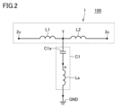
- FIG. 2 is a perspective view of a coil component according to the first embodiment.
- 1 is a circuit diagram of a filter circuit including a coil component according to a first embodiment; 11A and 11B are diagrams for explaining a change in mutual inductance due to the shape of an intermediate terminal. 11A and 11B are diagrams for explaining a change in mutual inductance due to the shape of the housing.
- FIG. 11 is a perspective view of a coil component according to a second embodiment. 11 is a diagram for explaining the positional relationship of the opening planes of the coil.
- FIG. FIG. 13 is a perspective view of a coil component according to a first modified example.
- FIG. 11 is a perspective view of a coil component according to a second modified example. 13 is a diagram for explaining the positional relationship of the opening plane of the coil according to the second modification.
- FIG. FIG. 11 is an exploded plan view showing a configuration of a coil component according to Modification 3.
- Fig. 1 is a perspective view of the coil component 1 according to the first embodiment.
- Fig. 2 is a circuit diagram of a filter circuit 100 including the coil component 1 according to the first embodiment. Note that, with respect to the X-axis, Y-axis, and Z-axis defined in Fig. 1, the X-axis direction represents the left-right direction of the coil component 1, the Y-axis direction represents the front-rear direction of the coil component 1, and the Z-axis direction represents the up-down direction of the coil component 1, respectively.
- Coil component 1 is, for example, a transformer coil mounted in a filter circuit 100 used to reduce noise in power lines. As described below, coil component 1 magnetically couples two coils in order to cancel the parasitic inductance of a capacitor mounted in filter circuit 100. Furthermore, coil component 1 employs a structure in which the lead wires of the two coils are used to form a third coil.
- the coil component 1 includes a coil portion 2a (first coil) and a coil portion 3a (second coil) in a housing 4.
- the coil portion 2a is also referred to as coil L1
- the coil portion 3a is also referred to as coil L2.
- the coil portion 2a has one end connected to a lead wire 2b (first lead wire) and the other end connected to a lead wire 2d (second lead wire).
- the coil portion 3a has one end connected to a lead wire 3b (third lead wire) and the other end connected to a lead wire 3d (fourth lead wire).
- the coil portion 2a and the lead wires 2b and 2d are formed of a single conductor, and are formed of a metal plate or metal wire of, for example, copper or an alloy of copper and other metals.
- the coil portion 3a and the lead wires 3b and 3d are also formed of a single conductor.
- the coils L1 and L2 formed from metal plates are covered with an insulating material not shown.
- the insulating material that covers coil L1 and coil L2 is a resin such as polyimide, epoxy, etc. Note that the insulating material does not need to cover all surfaces of coil L1 and coil L2. In order to prevent contact between coil L1 and coil L2, it is sufficient that the insulating material is provided at least on the surfaces where coil L1 and coil L2 face each other.
- the coil portion 2a has a rectangular opening and is disposed inside the housing 4 approximately parallel to the main surface 40A (first main surface).
- the coil portion 2a is illustrated as a single-turn coil, but may be a multiple-turn coil.
- the lead wire 2d and the lead wire 2d are drawn out from the side surface 41 (first side surface) of the housing 4 and extend along the side surface 41 toward the main surface 40B (second main surface).
- the lead wire 2b shown in FIG. 1 is provided up to the main surface 40B, and the portion that contacts the main surface 40B constitutes the end portion 2c.
- the lead wire 2d is provided up to the main surface 40B, and the portion that contacts the main surface 40B constitutes the end portion 2e.
- the coil portion 3a has a rectangular opening and is disposed above the coil portion 2a inside the housing 4, approximately parallel to the main surface 40A.
- the coil portion 3a is illustrated as a one-turn coil, but may be a multiple-turn coil.
- the lead wire 3d and the lead wire 3d are drawn out from the side surface 42 (second side surface) of the housing 4 and extend along the side surface 42 in the direction of the main surface 40B.
- the lead wire 3b shown in FIG. 1 is provided up to the main surface 40B, and the portion that contacts the main surface 40B constitutes the end portion 3c.
- the lead wire 3d is provided up to the main surface 40B, and the portion that contacts the main surface 40B constitutes the end portion 3e.
- the end portion 3c When the coil component 1 is mounted on the board, the end portion 3c is electrically connected to the wiring on the board.
- the end portions 2e and 3e are electrically connected by a connection member 5 disposed on the main surface 40B.
- Coil L1 and coil L2 are connected in series by connecting end 2e and end 3e with connecting member 5, and ends 2e, 3e and connecting member 5 form an intermediate terminal T between coil L1 and coil L2.
- Coil L1 and coil L2 are disposed inside housing 4 closer to main surface 40A than main surface 40B.
- coil L1 and coil L2 are disposed closer to main surface 40A than the midpoint between main surfaces 40A and 40B. This allows the length of lead wire 2d extending from the other end of coil portion 2a to main surface 40B, and the length of lead wire 3d extending from the other end of coil portion 3a to main surface 40B to be increased, allowing the opening of the coil (coil L3) formed by lead wire 2d, lead wire 3d, and connecting member 5 to be increased.
- the coil portions 2a and 3a are arranged so as to overlap when viewed from the main surface 40A direction, the coils L1 and L2 are magnetically coupled.
- the coil (coil L3) formed by the drawer 2d, the drawer 3d, and the connection member 5 generates a magnetic field in the +X direction.
- Figure 1 shows an example in which the openings almost overlap, but as long as the magnetic field coupling is within the range, the openings may be offset from each other, and it is sufficient that each opening overlaps by 50% or more.
- the housing 4 fixes the relative positions of the coil L1 and the coil L2, and is made of, for example, molded resin.
- the molded resin is made of various resins, such as epoxy resin with added silica filler, silicone resin, liquid crystal polymer, or metal magnetic material.
- the housing 4 has a side 41 (first side) and a side 42 (second side) that face each other, and the side closer to the lead wire 2b (first lead wire) is called side 43 (third side), and the side closer to the lead wire 2d (second lead wire) is called side 44 (fourth side).
- the side may be inclined as long as the second main surface, which is the mounting surface, and the coil surface are approximately parallel, and may be, for example, a trapezoid in which the area of the second main surface is larger than that of the first main surface.
- the filter circuit 100 is, for example, an EMI removal filter as shown in FIG. 2, and is a third-order T-type LC filter circuit.
- the filter circuit 100 has an end 2c connected to a power source (not shown) and an end 3c connected to a circuit (not shown) such as a DC/DC converter or a power supply module.
- the filter circuit 100 passes necessary components of the current flowing from the power source to the circuit and removes unnecessary components. Specifically, a direct current is passed through the filter circuit 100, and high-frequency noise contained in the direct current is dropped to GND through the capacitor C1.
- the capacitor C1 which is a capacitance element, has an equivalent series inductance ESL (La) of the capacitor C1, which prevents high-frequency noise from passing through, thereby degrading the noise removal performance.
- the filter circuit 100 uses the negative inductance generated by the magnetic coupling of the two coils to cancel the ESL (La) of the capacitor C1 and maintains high noise removal performance.
- the negative inductance generated in series with the capacitor C1 is called the mutual inductance M of the coil component 1.
- the filter circuit 100 will be described using a third-order T-type LC filter circuit, but coil components of a similar configuration can also be applied to a fifth-order T-type LC filter circuit or a higher-order T-type LC filter circuit.
- the filter circuit 100 includes a capacitor C1, ends 2c and 3c, an intermediate terminal T (ends 2e and 3e, connecting member 5), a coil L1, and a coil L2.
- the capacitor C1 has one end connected to the intermediate terminal T and the other end connected to the GND wiring.
- the capacitor C1 may be a multilayer ceramic capacitor mainly made of BaTiO 3 (barium titanate), a multilayer ceramic capacitor mainly made of other materials, or another type of capacitor such as an aluminum electrolytic capacitor.
- the capacitor C1 has an inductor La as a parasitic inductance (equivalent series inductance (ESL)), and is equivalent to a circuit configuration in which the inductor La is connected in series to the capacitor C1a.
- the capacitor C1 may also be equivalent to a circuit configuration in which a parasitic resistance (equivalent series resistance (ESR)) is connected in series to the inductor La and the capacitor C1a.
- coils L1 and L2 are connected to the intermediate terminal T. Coils L1 and L2 are magnetically coupled and have a mutual inductance M. A negative inductance component of the same magnitude as the mutual inductance M is generated between the intermediate terminal T and the capacitor C1. This negative inductance component can be used to cancel out the parasitic inductance (inductor La) of the capacitor C1, making the parasitic inductance component of the capacitor C1 appear smaller.
- the filter circuit 100 which is composed of the capacitor C1, coil L1, and coil L2, can cancel out the parasitic inductance of the capacitor C1 with the negative inductance component due to the mutual inductance between coils L1 and L2, thereby suppressing the decrease in the noise suppression effect in the high frequency band due to the parasitic inductance of the capacitor C1 and improving the noise suppression effect of the filter circuit 100.
- a coil (coil L3) is formed with the draw-out wires 2d and 3d and the connection member 5 and connected to the capacitor C1. Specifically, it is electrically connected to the wiring on the board by the connection member 5 and connected to the capacitor C1 which is electrically connected to the same wiring.
- the coil L3 itself connected to the capacitor C1 is also combined with the coils L1 and L2 as part of the coils, so it contributes to the negative inductance component due to the mutual inductance between the coils L1 and L2 and does not reduce the negative inductance component. It may be the end 2e connected to the draw-out wire 2d or the end 3e connected to the draw-out wire 3d that is connected to the wiring on the board, instead of the connection member 5.
- the intermediate terminal T which is the part connecting the coil L1 and the coil L2, is a coil (coil L3) composed of the lead wire 2d, the lead wire 3d, and the connection member 5, so that the three coils L1 to L3 have a relationship with a positive coupling coefficient.
- the connection member 5 is described as being disposed on the main surface 40B, but the connection member 5 may be provided on the board side on which the coil component 1 is mounted.
- the coil component 1 itself does not constitute a coil (coil L3) because the lead wire 2d and the lead wire 3d are not electrically connected, but the coil (coil L3) may be constituted by mounting the coil component 1 on a board on which the connection member 5 is provided.
- connection member 5 Even if the coil component 1 does not have the connection member 5, by mounting it on a board on which the connection member 5 is provided, there is no need to draw a wire from the intermediate terminal T and connect it to the capacitor C1, so the negative inductance component due to the mutual inductance between the coil L1 and the coil L2 is not reduced by the wire.
- FIG. 3 is a diagram for explaining the change in mutual inductance depending on the shape of the intermediate terminal.
- FIG. 3(a) is a diagram showing a schematic diagram of the shape of the intermediate terminal of coil component 1.
- the shape of intermediate terminal T that connects to capacitor C1 (not shown) is coil L3, so that the inductance component of coil L3 is added to the transformer coil composed of coils L1 and L2.
- the mutual inductance M of coil component 1 becomes high.
- the size of coil component 1 is 2.5 ⁇ 2.0 ⁇ 1.5 mm and the inductance value of coils L1 and L2 is approximately 3 nH
- Figure 3(b) is a schematic diagram showing a configuration in which a wiring 6 is extended from intermediate terminal T in a comparative coil component 11 to connect to a capacitor C1 (not shown).
- the wiring 6 for connecting to capacitor C1 has a positive parasitic inductance, which is offset by the mutual inductance M between coils L1 and L2, resulting in a low mutual inductance M of coil component 11.
- the inductance values of coils L1 and L2 are the same as those of coil component 1 shown in Figure 3(a) and the length of wiring 6 is 1.0 mm
- FIG. 4 is a diagram for explaining the change in mutual inductance M depending on the shape of the housing.
- Figure 4(a) is a perspective view of coil component 1A in which coils L1 and L2 are enclosed in housing 4A whose main surface 40A is a rectangle with long sides 4L and short sides 4W.
- lead wires 2b and 2d and lead wires 3b and 3d are drawn out from the side surface on the short side 4W side. Therefore, in coil component 1A, the side surface on the long side 4L side becomes the opening of coil L3.
- FIG. 4(b) is a perspective view of coil component 1B in which lead wires 2b, 2d and lead wires 3b, 3d are drawn out from the side surface of long side 4L of housing 4A.
- lead wires 2b, 2d and lead wires 3b, 3d are drawn out from the side surface of long side 4L. Therefore, in coil component 1B, the side surface of short side 4W becomes the opening of coil L3.
- the size of coil component 1B and the distance between coils L1 and L2 are the same as those of coil component 1A shown in FIG. 4(a).
- FIG. 4(c) is a perspective view of coil component 1C, in which coils L1 and L2 are housed in housing 4B, which has a shorter height 4H than housing 4A.
- leads 2b and 2d and leads 3b and 3d are drawn out from the side surface on the short side 4W side. Therefore, in coil component 1C, the side surface on the long side 4L side becomes the opening for coil L3.
- short side 4W 2.0 mm
- height 4H 0.9 mm
- the distance between coils L1 and L2 0.02 mm
- FIG. 4(d) is a perspective view of coil component 1D in which lead wires 2b, 2d and lead wires 3b, 3d are drawn out from the side surface of long side 4L of housing 4B.
- lead wires 2b, 2d and lead wires 3b, 3d are drawn out from the side surface of long side 4L. Therefore, in coil component 1D, the side surface of short side 4W becomes the opening of coil L3.
- the size of coil component 1D and the distance between coils L1 and L2 are the same as coil component 1C shown in FIG. 4(c).
- the coil component 1 includes a housing 4 having a pair of opposing main surfaces 40A and 40B and four side surfaces 41 to 44 connecting the main surfaces 40A and 40B, a coil L1 disposed inside the housing 4 and disposed substantially parallel to the main surface 40A, and a coil L2 disposed inside the housing 4 such that the openings of the coil L1 overlap when viewed from the direction of the main surface 40A.
- the coil L1 has a lead wire 2b and a lead wire 2d drawn out from the side surface 41 of the housing 4.
- the coil L2 has a lead wire 3b and a lead wire 3d drawn out from the side surface 42 different from the side surface 41.
- the lead wire 2d extends in the direction of the main surface 40B along the side surface 41.
- the lead wire 3d extends in the direction of the main surface 40B along the side surface 42.
- extending along the side surface means extending substantially parallel to the side surface.
- the draw-out wire 2d of the coil L1 extends in the direction of the main surface 40B along the side surface 41 where it is drawn out
- the draw-out wire 3d of the coil L2 extends in the direction of the main surface 40B along the side surface 42 where it is drawn out, so that it is possible to form a coil with the draw-out wires 2d and 3d, and there is no reduction in the negative inductance that occurs when the two coils L1 and L2 are magnetically coupled.
- the lead wires 2b and 2d are drawn out from the side surface 41 to the outside of the housing 4. However, as long as the lead wires 2b and 2d are drawn out to the side surface 41, the coil component 1 does not have to be drawn out to the outside of the housing 4, and the lead wires 2b and 2d may be inside the housing 4. Similarly, in the coil component 1, the lead wires 3b and 3d are drawn out from the side surface 42 to the outside of the housing 4. However, as long as the lead wires 3b and 3d are drawn out to the side surface 42, the coil component 1 does not have to be drawn out to the outside of the housing 4, and the lead wires 3b and 3d may be inside the housing 4.
- the filter circuit 100 includes the coil component 1 described above, and a capacitor C1 electrically connected to the intermediate terminals (lead wire 2d, lead wire 3d) between coil L1 and coil L2 of coil component 1.
- the filter circuit 100 can fully cancel the parasitic inductance of the capacitor C1 with the negative inductance generated by magnetically coupling the two coils L1 and L2, and can achieve a wideband noise suppression effect.
- FIG. 5 is a perspective view of a coil component 1E according to the second embodiment. Note that in the coil component 1E shown in the second embodiment, the same components as those in the coil component 1 according to the first embodiment are designated by the same reference numerals and detailed description will not be repeated. Also, the coil component 1E shown in the second embodiment can be applied to the filter circuit 100 according to the first embodiment in place of the coil component 1 according to the first embodiment.
- coil component 1E As shown in FIG. 5, in coil component 1E, lead wires 2d and 3d extend almost straight from the lead-out position toward main surface 40B. Therefore, the opening surface of the coil (coil L3) formed by lead wires 2d, 3d and connecting member 5 is perpendicular (90 degrees) to the opening surfaces of coils L1 and L2.
- Lead-out lines 2b and 2d are drawn out from side 41 on the side of side 44.
- Lead-out lines 3b and 3d are drawn out from side 42 on the side of side 44.
- coil component 1E is contained within housing 4 with the lead-out positions of lead-out lines 2b, 2d, and lead-out lines 3b, 3d from coil portions 2a, 3a shifted toward side 44.
- the state in which the lead wires 2b and 2d are closer to the side surface 44 means that the area between the connection point of the coil portion 2a and the lead wire 2b and the connection point of the coil portion 2a and the lead wire 2d is located closer to the side surface 44 than the midpoint between the side surfaces 43 and 44.
- the end of the lead wire 2d on the main surface 40B side is on the side surface 41 on the side surface 44 side.
- the lead wire 2d is drawn out from a position between the width of the end 2e.
- the end of the lead wire 3d on the main surface 40B side is on the side surface 42 on the side surface 44 side.
- the lead wire 3d is drawn out from a position between the width of the end 3e.
- the lead wires 2d and 3d are approximately straight lines extending from the drawn-out position toward the main surface 40B side. Therefore, the coil (coil L3) formed by the lead wire 2d, the lead wire 3d and the connecting member 5 is formed parallel to the side surface 44.
- coil component 1 As shown in FIG. 1, lead wires 2b and 2d are drawn out from the middle part of side 41 between side 43 and side 44, and lead wires 3b and 3d are drawn out from the middle part of side 42 between side 43 and side 44.
- coil sections 2a and 3a are contained in housing 4 between side 43 and side 44, and lead wires 2b and 2d, as well as lead wires 3b and 3d, are drawn out from the middle part of the side between side 43 and side 44.
- drawn out from the middle part means that a point in the region between the connection point of coil section 2a and lead wire 2b and the connection point of coil section 2a and lead wire 2d overlaps with the middle position of side 43 and side 44.
- the end of lead-out wire 2d on the main surface 40B side is on side surface 41 on the side surface 44 side.
- the end of lead-out wire 3d on the main surface 40B side is on side surface 42 on the side surface 44 side.
- lead-out wires 2d and 3d extend from the lead-out position obliquely toward side surface 44 toward main surface 40B. Therefore, the coil (coil L3) formed by lead-out wires 2d, 3d and connecting member 5 is formed inclined with respect to side surface 44.
- the opening surface of coil L3 is inclined by more than 90 degrees with respect to the opening surfaces of coils L1 and L2.
- FIG. 6 is a diagram for explaining the positional relationship of the opening surfaces of the coils.
- FIG. 6(a) is a schematic diagram showing the positional relationship between the opening surface of coil L3 and the opening surfaces of coils L1 and L2 of coil component 1E.
- coils L1 and L2 are arranged parallel to the X-Y plane, and coil L3 is arranged parallel to the Y-Z plane.
- the angle ⁇ between the direction of the magnetic field G1 generated by coils L1 and L2 and the direction of the magnetic field G2 generated by coil L3 is 90 degrees.
- FIG. 6(b) is a schematic diagram showing the positional relationship between the opening surface of coil L3 of coil component 1 and the opening surfaces of coils L1 and L2.
- coil component 1 coils L1 and L2 are arranged parallel to the X-Y plane, and coil L3 is arranged tilted in the X direction from a position parallel to the Y-Z plane.
- the angle ⁇ between the direction of magnetic field G1 generated by coils L1 and L2 and the direction of magnetic field G2 generated by coil L3 is greater than 90 degrees.
- the direction of magnetic field G2 includes a directional component opposite to the direction of magnetic field G1, and the coupling coefficient of the three coils L1 to L3 decreases. Therefore, by setting the angle ⁇ between the directions of magnetic fields G1 and G2 to 90 degrees, as in coil component 1E, the directional component opposite to the direction of magnetic field G1 in the direction of magnetic field G2 is reduced, and the coupling coefficient of the three coils L1 to L3 can be increased.
- coil component 1E contributes to the negative inductance component due to the mutual inductance between coils L1 and L2, and does not reduce the negative inductance component.
- FIG. 7 is a perspective view of the coil component 1F according to the first modification.
- the same reference numerals are used for the same configuration as the coil component 1 according to the first embodiment, and detailed description will not be repeated. Also, the coil component 1F shown in the first modification can be applied to the filter circuit 100 according to the first embodiment in place of the coil component 1 according to the first embodiment.
- coil component 1F lead wires 2d and 3d extend straight from their drawn-out positions toward main surface 40B. Therefore, the opening surface of the coil (coil L3) formed by lead wires 2d, 3d and connecting member 5 is perpendicular (90 degrees) to the opening surfaces of coils L1 and L2.
- coil component 1F lead wires 2b and 2d are drawn out from the middle part of side 41 between side 43 and side 44, and lead wires 3b and 3d are drawn out from the middle part of side 42 between side 43 and side 44.
- coil portions 2a and 3a are contained within housing 4 midway between side 43 and side 44, and lead wires 2b, 2d, and lead wires 3b, 3d are also drawn out from the middle parts of the side between side 43 and side 44.
- lead wire 2d has its end on the main surface 40B side located in the middle of side surface 41 between side surfaces 43 and 44
- lead wire 3d has its end on the main surface 40B side located in the middle of side surface 42 between side surfaces 43 and 44.
- lead wires 2d and 3d are straight lines that extend from their drawn-out positions toward the main surface 40B. Therefore, the coil (coil L3) formed by lead wires 2d, 3d and connecting member 5 is formed parallel to side surface 44.
- coil component 1F the opening surface of coil L3 is perpendicular (90 degrees) to the opening surfaces of coils L1 and L2 at the center of coils L1 and L2.
- coil component 1E as shown in FIG. 5, the opening surface of coil L3 is perpendicular (90 degrees) to the opening surfaces of coils L1 and L2 at the ends of coils L1 and L2. Therefore, coil component 1E can achieve a higher coupling coefficient between the three coils L1 to L3 than coil component 1F.
- FIG. 6A In the coil component 1, as shown in FIG. 6A, the coil L3 is arranged so that the angle ⁇ between the direction of the magnetic field G1 and the direction of the magnetic field G2 is greater than 90 degrees.
- the coil L3 In the coil component 1E, as shown in FIG. 6B, the coil L3 is arranged so that the angle ⁇ between the direction of the magnetic field G1 and the direction of the magnetic field G2 is 90 degrees.
- the coil L3 is arranged so that the angle ⁇ between the direction of the magnetic field G1 and the direction of the magnetic field G2 is smaller than 90 degrees.
- FIG. 8 is a perspective view of the coil component 1G according to the second modification.
- the same reference numerals are used for the same configuration as the coil component 1 according to the first embodiment, and detailed description will not be repeated. Also, the coil component 1G shown in the second modification can be applied to the filter circuit 100 according to the first embodiment in place of the coil component 1 according to the first embodiment.
- coil component 1G lead wires 2d and 3d extend obliquely from the lead-out position toward main surface 40B. Therefore, the opening surface of the coil (coil L3) formed by lead wires 2d, 3d and connecting member 5 is at an angle of less than 90 degrees to the opening surfaces of coils L1 and L2.
- Pull-out wire 2b is pulled out from side surface 41 on the side surface 43 side. Pull-out wire 2d is pulled out through the inside of the housing 4 in order to be pulled further from side surface 43 to side surface 41 side than pull-out wire 2b. Similarly, pull-out wire 3b is pulled out from side surface 42 on the side surface 43 side. Pull-out wire 3d is pulled out through the inside of the housing 4 in order to be pulled further from side surface 43 to side surface 42 side than pull-out wire 3b. In other words, pull-out wire 2b and pull-out wire 3b are pulled out to the outside of the housing 4, and pull-out wire 2d and pull-out wire 3d are pulled into the housing 4. Pull-out wire 2b and pull-out wire 2d cross each other midway, and pull-out wire 3b and pull-out wire 3d cross each other midway.
- the end of the lead wire 2d on the main surface 40B side is on the side surface 41 side of the side surface 44.
- the end of the lead wire 3d on the main surface 40B side is on the side surface 42 side of the side surface 44.
- the lead wires 2d and 3d extend obliquely from the lead position toward the side surface 44 side toward the main surface 40B side.
- the end of the lead wire 2d and the end of the lead wire 3d are electrically connected via a connection member 5a arranged in the housing 4. Therefore, the coil (coil L3) formed by the lead wires 2d, 3d and the connection member 5a is formed inclined with respect to the side surface 44.
- the opening surface of the coil L3 is inclined at an angle of less than 90 degrees with respect to the opening surfaces of the coils L1 and L2.
- FIG. 9 is a diagram for explaining the positional relationship of the opening surfaces of the coils according to variant example 2.
- FIG. 9 is a schematic diagram showing the positional relationship between the opening surface of coil L3 and the opening surfaces of coils L1 and L2 of coil component 1G.
- coil component 1G coils L1 and L2 are arranged parallel to the X-Y plane, and coil L3 is arranged tilted in the X direction from a position parallel to the Y-Z plane.
- the angle ⁇ between the direction of magnetic field G1 generated by coils L1 and L2 and the direction of magnetic field G2 generated by coil L3 is less than 90 degrees.
- the direction of magnetic field G2 includes a directional component in the same direction as magnetic field G1, and the coupling coefficient of the three coils L1 to L3 increases. Therefore, by making the angle ⁇ between the directions of magnetic fields G1 and G2 less than 90 degrees, as in coil component 1G, the number of directional components in the same direction as magnetic field G1 in the direction of magnetic field G2 can be increased, and the coupling coefficient of the three coils L1 to L3 can be increased.
- the coil portion 2a and the lead wires 2b, 2d are formed of one conductor (for example, a metal plate), and the coil portion 3a and the lead wires 3b, 3d are formed of one conductor. Furthermore, in the coil components, the coil portion 2a and the coil portion 3a formed of a conductor are fixed by the molding resin of the housing 4 at a position where they overlap, and the lead wires 2b, 2d, 3b, 3d drawn from the side of the housing 4 are bent along the side of the housing 4.
- the manufacturing method of the coil component is not limited to the above-mentioned method.
- Modification 3 a coil component in which the coil is not formed of one conductor but is manufactured by stacking multiple substrates (ceramic green sheets) on which the coil wiring is formed is described.
- FIG. 10 is an exploded plan view showing the configuration of a coil component according to Modification 3. Note that in the coil component shown in Modification 3, the same components as those in coil component 1 according to embodiment 1 are designated by the same reference numerals and will not be described in detail again. Also, the coil component shown in Modification 3 can be applied to the filter circuit 100 according to embodiment 1 in place of coil component 1 according to embodiment 1.
- the coil component of the third modification is composed of a ceramic layer housing 4 in which multiple substrates (ceramic green sheets) on which coil wiring is formed are stacked as shown in FIG. 10.
- the wiring patterns constituting the coils L1 and L2 are disposed inside the housing 4.
- the wiring patterns constituting the coils L1 and L2 are formed by printing a conductive paste (Ni paste) by screen printing on the ceramic green sheets 4a to 4j, which are the substrates.
- FIG. 10(a) no wiring pattern is formed on the ceramic green sheet 4a.
- FIG. 10(b) a wiring pattern of the coil portion 3a and the lead wires 3b and 3d that constitute the coil L2 is formed on the ceramic green sheet 4b.
- the wiring pattern of the coil portion 3a is formed so as to go around each side of the ceramic green sheet 4b.
- the wiring pattern of the lead wires 3b and 3d is drawn out from the coil portion 3a to the side surface 42 of the ceramic green sheet 4b.
- the wiring pattern of the coil portion 2a and the lead wires 2b and 2d that constitute the coil L1 is formed on the ceramic green sheet 4c.
- the wiring pattern of the coil portion 2a is formed so as to go around each side of the ceramic green sheet 4c.
- the wiring pattern of the lead wires 2b and 2d is drawn out from the coil portion 2a to the side surface 41 of the ceramic green sheet 4c.
- the wiring pattern of the lead wires 3b and 3d is formed on the side surface 42 of the ceramic green sheet 4c.
- the ceramic green sheets 4d to 4i have wiring patterns for the lead wires 2b and 2d formed on the side 41 side, and wiring patterns for the lead wires 3b and 3d formed on the side 42 side.
- the ceramic green sheet 4j is formed with a wiring pattern of the ends 2c, 2e, 3c, and 3e that constitute the ends of the lead wires 2b, 2d, 3b, and 3d, as shown in FIG. 10(j).
- the wiring pattern of the ends 2c and 2e is formed on the side 41 of the ceramic green sheet 4j, and the wiring pattern of the ends 3c and 3e is formed on the side 42.
- the ceramic green sheet 4j is formed with a wiring pattern of the connection member 5 that connects the ends 2e and 3e.
- At least one of the plurality of ceramic green sheets 4a to 4j is laminated, and a plurality of ceramic green sheets (dummy layers) without printed wiring patterns are laminated on both the top and bottom sides.
- the plurality of ceramic green sheets, including the dummy layers, are pressed together to form an unfired housing 4 (ceramic body).
- the formed housing 4 is fired, and copper electrodes are baked onto the outside of the fired housing 4 so as to be conductive to the wiring patterns, forming electrodes.
- the coil component of variant 3 is manufactured not by fixing coil L1 and coil L2 formed from metal plates with the molding resin of the housing 4, but by stacking multiple substrates (ceramic green sheets) on which the coil wiring is formed.
- a coil component includes a housing having a pair of first and second main surfaces opposed to each other and four side surfaces connecting the first and second main surfaces;
- a first coil is disposed inside the housing and disposed substantially parallel to the first main surface;
- a second coil disposed inside the housing such that an opening of the first coil overlaps an opening of the second coil when viewed from the direction of the first main surface, the first coil is connected to a first lead wire and a second lead wire that are led out from a first side surface side of the housing;
- the second coil is connected to a third lead wire and a fourth lead wire that are led out from a second side surface different from the first side surface;
- the second lead line extends along the first side surface toward the second main surface,
- the fourth lead line extends along the second side surface toward the second main surface.
- the coil component according to (1), The first coil and the second coil are disposed inside the housing closer to the first main surface than the second main surface.
- the coil component according to (2), The first coil and the second coil are disposed on the first principal surface side from a middle position between the first principal surface and the second principal surface.
- the semiconductor device further includes a connection member disposed on the second main surface and electrically connecting the second lead wire and the fourth lead wire.
- the second lead wire has an end portion on the second main surface side located in a middle portion of the first side surface between the third side surface and the fourth side surface;
- the fourth lead wire has an end portion on the second main surface side located in a middle portion of the second side surface between the third side surface and the fourth side surface.
- the coil component according to (6), The second lead wire has an end portion on the second main surface side that is on the first side surface side of the fourth side surface side,
- the fourth lead wire has an end on the second main surface side on the second side surface side of the fourth side surface side.
- the coil component according to any one of (1) to (10), The first coil and the second coil are formed from a metal plate or a metal wire.
- a filter circuit according to the present disclosure includes the coil component according to any one of (1) to (12), and a capacitor electrically connected to the second lead wire and the fourth lead wire of the coil component.
Landscapes
- Engineering & Computer Science (AREA)
- Power Engineering (AREA)
- Microelectronics & Electronic Packaging (AREA)
- Coils Or Transformers For Communication (AREA)
Priority Applications (2)
| Application Number | Priority Date | Filing Date | Title |
|---|---|---|---|
| JP2024571613A JP7750436B2 (ja) | 2023-01-19 | 2023-09-26 | コイル部品、これを含むフィルタ回路 |
| US19/217,183 US20250309850A1 (en) | 2023-01-19 | 2025-05-23 | Coil component and filter circuit including the same |
Applications Claiming Priority (2)
| Application Number | Priority Date | Filing Date | Title |
|---|---|---|---|
| JP2023006740 | 2023-01-19 | ||
| JP2023-006740 | 2023-01-19 |
Related Child Applications (1)
| Application Number | Title | Priority Date | Filing Date |
|---|---|---|---|
| US19/217,183 Continuation US20250309850A1 (en) | 2023-01-19 | 2025-05-23 | Coil component and filter circuit including the same |
Publications (1)
| Publication Number | Publication Date |
|---|---|
| WO2024154387A1 true WO2024154387A1 (ja) | 2024-07-25 |
Family
ID=91955766
Family Applications (1)
| Application Number | Title | Priority Date | Filing Date |
|---|---|---|---|
| PCT/JP2023/034859 Ceased WO2024154387A1 (ja) | 2023-01-19 | 2023-09-26 | コイル部品、これを含むフィルタ回路 |
Country Status (3)
| Country | Link |
|---|---|
| US (1) | US20250309850A1 (https=) |
| JP (1) | JP7750436B2 (https=) |
| WO (1) | WO2024154387A1 (https=) |
Citations (6)
| Publication number | Priority date | Publication date | Assignee | Title |
|---|---|---|---|---|
| US20080174396A1 (en) * | 2007-01-24 | 2008-07-24 | Samsung Electronics Co., Ltd. | Transformers and baluns |
| JP2012015493A (ja) * | 2010-05-31 | 2012-01-19 | Tdk Corp | コイル部品及びその製造方法 |
| JP2012256757A (ja) * | 2011-06-09 | 2012-12-27 | Tdk Corp | Lc複合部品及びlc複合部品の実装構造 |
| JP2016213344A (ja) * | 2015-05-11 | 2016-12-15 | パナソニックIpマネジメント株式会社 | ノイズ抑制部品 |
| JP2020174112A (ja) * | 2019-04-10 | 2020-10-22 | 株式会社村田製作所 | 複合部品 |
| WO2020246028A1 (ja) * | 2019-06-07 | 2020-12-10 | 三菱電機株式会社 | ノイズフィルタ及び電源装置 |
Family Cites Families (3)
| Publication number | Priority date | Publication date | Assignee | Title |
|---|---|---|---|---|
| JP6753164B2 (ja) * | 2016-06-21 | 2020-09-09 | 株式会社村田製作所 | ノイズ対策部品、及び、ノイズ対策モジュール |
| WO2021085002A1 (ja) * | 2019-10-30 | 2021-05-06 | 株式会社村田製作所 | コイル部品および、これを含むフィルタ回路 |
| JP7107463B1 (ja) * | 2020-10-01 | 2022-07-27 | 株式会社村田製作所 | 電子機器 |
-
2023
- 2023-09-26 JP JP2024571613A patent/JP7750436B2/ja active Active
- 2023-09-26 WO PCT/JP2023/034859 patent/WO2024154387A1/ja not_active Ceased
-
2025
- 2025-05-23 US US19/217,183 patent/US20250309850A1/en not_active Abandoned
Patent Citations (6)
| Publication number | Priority date | Publication date | Assignee | Title |
|---|---|---|---|---|
| US20080174396A1 (en) * | 2007-01-24 | 2008-07-24 | Samsung Electronics Co., Ltd. | Transformers and baluns |
| JP2012015493A (ja) * | 2010-05-31 | 2012-01-19 | Tdk Corp | コイル部品及びその製造方法 |
| JP2012256757A (ja) * | 2011-06-09 | 2012-12-27 | Tdk Corp | Lc複合部品及びlc複合部品の実装構造 |
| JP2016213344A (ja) * | 2015-05-11 | 2016-12-15 | パナソニックIpマネジメント株式会社 | ノイズ抑制部品 |
| JP2020174112A (ja) * | 2019-04-10 | 2020-10-22 | 株式会社村田製作所 | 複合部品 |
| WO2020246028A1 (ja) * | 2019-06-07 | 2020-12-10 | 三菱電機株式会社 | ノイズフィルタ及び電源装置 |
Also Published As
| Publication number | Publication date |
|---|---|
| US20250309850A1 (en) | 2025-10-02 |
| JPWO2024154387A1 (https=) | 2024-07-25 |
| JP7750436B2 (ja) | 2025-10-07 |
Similar Documents
| Publication | Publication Date | Title |
|---|---|---|
| CN216162684U (zh) | 线圈部件及包含该线圈部件的滤波器电路 | |
| US12355416B2 (en) | Coil component, filter circuit including the coil component, and electronic device | |
| CN205080956U (zh) | 电感元器件、电感电桥以及高频滤波器 | |
| CN219164535U (zh) | 滤波器电路以及包含该滤波器电路的电源装置 | |
| JP6458903B2 (ja) | 受動素子アレイおよびプリント配線板 | |
| US20240428985A1 (en) | Circuit device and filter circuit | |
| US11870412B2 (en) | Multilayer substrate, circuit device, and filter circuit substrate | |
| JP6500989B2 (ja) | 回路基板、これを用いたフィルタ回路およびキャパシタンス素子 | |
| US10284164B2 (en) | Circuit substrate, filter circuit, and capacitance element | |
| CN114334351B (zh) | 线圈部件 | |
| JP7553470B2 (ja) | 回路装置、およびフィルタ回路 | |
| US20240297631A1 (en) | Circuit device | |
| JP7750436B2 (ja) | コイル部品、これを含むフィルタ回路 | |
| WO2024154782A1 (ja) | コイル部品、フィルタ回路、および回路装置 | |
| JP7694825B2 (ja) | コイル部品、およびこれを含むフィルタ回路 | |
| WO2026048259A1 (ja) | コイル部品、これを含む電子機器 | |
| WO2025047045A1 (ja) | コイル部品、これを含む回路装置 | |
| WO2024154388A1 (ja) | コイル部品、およびフィルタ回路 | |
| WO2024166971A1 (ja) | 回路装置、および回路基板 | |
| WO2024172015A1 (ja) | コイル部品、これを含むフィルタ回路 | |
| US20250309852A1 (en) | Filter device | |
| WO2025083974A1 (ja) | コイル部品、およびフィルタ回路 | |
| JP2026025197A (ja) | 電子部品 | |
| JP2025172409A (ja) | コイル部品および、これを含むフィルタ回路 |
Legal Events
| Date | Code | Title | Description |
|---|---|---|---|
| 121 | Ep: the epo has been informed by wipo that ep was designated in this application |
Ref document number: 23917599 Country of ref document: EP Kind code of ref document: A1 |
|
| WWE | Wipo information: entry into national phase |
Ref document number: 2024571613 Country of ref document: JP |
|
| NENP | Non-entry into the national phase |
Ref country code: DE |
|
| 122 | Ep: pct application non-entry in european phase |
Ref document number: 23917599 Country of ref document: EP Kind code of ref document: A1 |