WO2024150690A1 - 固体撮像装置 - Google Patents
固体撮像装置 Download PDFInfo
- Publication number
- WO2024150690A1 WO2024150690A1 PCT/JP2023/047039 JP2023047039W WO2024150690A1 WO 2024150690 A1 WO2024150690 A1 WO 2024150690A1 JP 2023047039 W JP2023047039 W JP 2023047039W WO 2024150690 A1 WO2024150690 A1 WO 2024150690A1
- Authority
- WO
- WIPO (PCT)
- Prior art keywords
- signal processing
- solid
- state imaging
- imaging device
- event detection
- Prior art date
- Legal status (The legal status is an assumption and is not a legal conclusion. Google has not performed a legal analysis and makes no representation as to the accuracy of the status listed.)
- Ceased
Links
Classifications
-
- H—ELECTRICITY
- H04—ELECTRIC COMMUNICATION TECHNIQUE
- H04N—PICTORIAL COMMUNICATION, e.g. TELEVISION
- H04N23/00—Cameras or camera modules comprising electronic image sensors; Control thereof
- H04N23/50—Constructional details
- H04N23/54—Mounting of pick-up tubes, electronic image sensors, deviation or focusing coils
-
- H—ELECTRICITY
- H04—ELECTRIC COMMUNICATION TECHNIQUE
- H04N—PICTORIAL COMMUNICATION, e.g. TELEVISION
- H04N23/00—Cameras or camera modules comprising electronic image sensors; Control thereof
- H04N23/60—Control of cameras or camera modules
- H04N23/667—Camera operation mode switching, e.g. between still and video, sport and normal or high- and low-resolution modes
-
- H—ELECTRICITY
- H04—ELECTRIC COMMUNICATION TECHNIQUE
- H04N—PICTORIAL COMMUNICATION, e.g. TELEVISION
- H04N25/00—Circuitry of solid-state image sensors [SSIS]; Control thereof
- H04N25/47—Image sensors with pixel address output; Event-driven image sensors; Selection of pixels to be read out based on image data
-
- H—ELECTRICITY
- H04—ELECTRIC COMMUNICATION TECHNIQUE
- H04N—PICTORIAL COMMUNICATION, e.g. TELEVISION
- H04N25/00—Circuitry of solid-state image sensors [SSIS]; Control thereof
- H04N25/70—SSIS architectures; Circuits associated therewith
- H04N25/702—SSIS architectures characterised by non-identical, non-equidistant or non-planar pixel layout
-
- H—ELECTRICITY
- H04—ELECTRIC COMMUNICATION TECHNIQUE
- H04N—PICTORIAL COMMUNICATION, e.g. TELEVISION
- H04N25/00—Circuitry of solid-state image sensors [SSIS]; Control thereof
- H04N25/70—SSIS architectures; Circuits associated therewith
- H04N25/76—Addressed sensors, e.g. MOS or CMOS sensors
Definitions
- This disclosure relates to a solid-state imaging device.
- pixels that perform event detection can be arranged in a hybrid pixel array, making it possible to detect events and acquire color information in parallel on the same coordinate axis.
- one of the non-limiting problems that the embodiments of the present disclosure aim to solve is to correct distortion of event detection pixels.
- the problem that the embodiments of the present disclosure aim to solve can also be, as some further non-limiting examples, a problem that corresponds to the effects described in the embodiments.
- a problem that corresponds to at least any one of the effects described in the description of the embodiments of the present disclosure can be the problem that the present disclosure aims to solve.
- a solid-state imaging device includes an optical system, a first pixel, a second pixel, one or more pixel arrays, and a signal processing circuit.
- the first pixel acquires image information based on luminance information via the optical system.
- the second pixel acquires event detection information based on a change in luminance information via the optical system.
- the first pixels and the second pixels are arranged in a two-dimensional array.
- the signal processing circuit selects whether or not to perform distortion correction on the event detection information acquired by the second pixel, and executes signal processing.
- the one or more pixel arrays may be formed from a single pixel array;
- the second pixels may be arranged in a predetermined region in the pixel array at a predetermined ratio to the first pixels.
- the specified area may be the entire area of the pixel array.
- the second pixels may be arranged at equal intervals to cover the entire area of the specified region.
- the second pixel may detect an event every frame.
- the second pixel may detect an event using an arbiter method.
- the signal processing circuit may perform distortion correction of the image information.
- the signal processing circuit includes:
- the event detection information may be converted into a resolution of the image information.
- a distortion correction may be performed on the transformed event detection information.
- the signal processing circuit includes: Distortion correction of the event detection information may be performed based on a difference between a resolution of the event detection information and a resolution of the image information.
- the signal processing circuit includes: A region of interest may be set based on the image information, The event detection information corresponding to the region of interest may be obtained.
- the signal processing circuit includes: Tracking may be performed based on the distortion-corrected event detection information corresponding to the region of interest.
- the signal processing circuit includes: For coordinates after the distortion correction of the event detection information, a value obtained by correcting the distortion of the event detection information may be compared with a threshold value to obtain the event detection information at the coordinates after the distortion correction.
- the signal processing circuit includes: The event detection information at said coordinates after distortion correction may be stored as 1.5 bits of information.
- the one or more pixel array s a first pixel array in which the first pixels are arranged in a two-dimensional array; a second pixel array, the second pixels being arranged in a two-dimensional array and configured to acquire the event detection information of the same target as that of the first pixel array; It may be formed from
- the optical system includes: a first optical system that focuses light onto the first pixel array; a second optical system that focuses light onto the second pixel array; may also be provided.
- the signal processing circuit includes: a first signal processing circuit that processes a signal output from the first pixel; a second signal processing circuit that processes a signal output from the second pixel;
- the present invention may also include:
- the signal processing circuit includes: Image processing may be performed based on the distortion corrected image information and the distortion corrected event detection information.
- the signal processing circuit includes: A deblur process may be performed based on the distortion-corrected image information and the distortion-corrected event detection information.
- the signal processing circuit includes: A frame rate increasing process may be performed based on the distortion-corrected image information and the distortion-corrected event detection information.
- the signal processing circuit includes: A tracking process may be performed based on the distortion-corrected image information and the distortion-corrected event detection information.
- FIG. 1 is a block diagram illustrating a solid-state imaging device according to an embodiment.
- FIG. 2 is a block diagram illustrating an image capturing unit according to an embodiment.
- FIG. 2 is a diagram showing an example of a pixel arrangement in a pixel array according to an embodiment.
- FIG. 2 is a block diagram illustrating an image capturing unit according to an embodiment.
- FIG. 13 is a diagram showing an example of data transition according to an embodiment.
- 5 is a flowchart showing a process of a solid-state imaging device according to an embodiment.
- 5 is a flowchart showing a process of a solid-state imaging device according to an embodiment.
- 5 is a flowchart showing a process of a solid-state imaging device according to an embodiment.
- FIG. 1 is a block diagram illustrating a solid-state imaging device according to an embodiment.
- FIG. 2 is a block diagram illustrating an image capturing unit according to an embodiment.
- FIG. 2 is a diagram showing an example of a
- FIG. 13 is a diagram showing an example of setting a region of interest according to an embodiment
- 5 is a flowchart showing a process of a solid-state imaging device according to an embodiment.
- FIG. 1 is a block diagram illustrating a solid-state imaging device according to an embodiment.
- FIG. 2 is a diagram illustrating a substrate of a solid-state imaging device according to an embodiment.
- FIG. 2 is a diagram illustrating a substrate of a solid-state imaging device according to an embodiment.
- FIG. 2 is a diagram illustrating a substrate of a solid-state imaging device according to an embodiment.
- 1 is a block diagram showing an example of a schematic configuration of a vehicle control system; 4 is an explanatory diagram showing an example of the installation positions of an outside-vehicle information detection unit and an imaging unit;
- the solid-state imaging device 1 includes an optical system 10, an imaging unit 12, a storage unit 14, a signal processing unit 16, and an input/output interface (hereinafter, referred to as an input/output I/F 18).
- the solid-state imaging device 1 includes at least a first pixel that acquires image information from luminance information, and a second pixel that acquires event detection information from a change in the luminance information, and is a device that acquires image information and also acquires event detection information within the image.
- the optical system 10 is an optical system that appropriately focuses light onto the imaging unit 12.
- the imaging unit 12 has a first pixel and a second pixel, and acquires image information and event detection information. For example, the imaging unit 12 acquires information on an area that includes the same object in the first pixel and the second pixel.
- the memory unit 14 stores data acquired by the imaging unit 12, or data being processed by the signal processing unit 16 or data after processing.
- the memory unit 14 may include, for example, a memory circuit such as various memories or various storage devices that temporarily or non-temporarily stores data. At least a part of the memory unit 14 may be provided outside the solid-state imaging device 1.
- the signal processing unit 16 performs various processes on the data acquired by the imaging unit 12 and outputs the data. This process may include, for example, converting the analog signal output from the pixel circuit into a digital signal, acquiring pixel values from the digital signal, and performing image processing. Note that at least a part of the above processes may be executed in the pixel circuit of the imaging unit 12.
- the signal processing unit 16 may include, at least in part, a dedicated processing circuit such as an ASIC (Application Specified Integrated Circuitry), a general-purpose processing circuit such as a CPU (Central Processing Unit), or a programmable circuit such as an FPGA (Field Programmable Gate Array).
- a dedicated processing circuit such as an ASIC (Application Specified Integrated Circuitry)
- a general-purpose processing circuit such as a CPU (Central Processing Unit)
- a programmable circuit such as an FPGA (Field Programmable Gate Array).
- the processing executed by at least a part of the signal processing unit 16 may be in the form of information processing by software being specifically realized using hardware resources.
- a program or executable file related to the software is stored in the memory unit 14, and the general-purpose circuit of the signal processing unit 16 can acquire the program stored in the memory unit 14 to realize information processing.
- the input/output I/F 18 is an interface that connects the inside and outside of the solid-state imaging device 1.
- the solid-state imaging device 1 can accept control from the user directly or indirectly from the input/output I/F 18. Furthermore, the solid-state imaging device 1 can realize transmission and reception of data between the inside and outside via the input/output I/F 18.
- the solid-state imaging device 1 may be appropriately equipped with, for example, a control unit for controlling each component of the solid-state imaging device 1, a power supply unit for supplying power to each component, etc. as necessary.
- FIG. 2 is a schematic diagram showing a non-limiting example of the imaging unit 12.
- the imaging unit 12 includes a pixel array 120, a horizontal drive circuit 124, a vertical drive circuit 126, and a processing circuit 128.
- the imaging unit 12 appropriately processes and outputs signals acquired by pixels arranged in the pixel array 120.
- the pixel array 120 is formed by arranging pixels in a two-dimensional array.
- the pixel array 120 includes a first pixel that acquires luminance information and a second pixel that acquires changes in the luminance information.
- FIG. 3 is a diagram showing an example of the arrangement of pixels in the pixel array 120.
- the pixel array 120 is formed, for example, by cyclically arranging first pixels 121 and second pixels 122.
- the first pixel 121 includes a light receiving element that acquires luminance information, and each of these light receiving elements may be configured as a pixel that acquires one of the colors RGB.
- the color may be selected by a color filter provided on the light receiving element, or the light receiving element may be formed with an organic photoelectric conversion film or the like.
- the second pixel 122 has a light receiving element that acquires changes in luminance information as event detection information.
- the first pixels 121R, 121G, 121B and the second pixel 122 may form a pixel group as a single unit, and the first pixel 121 that acquires a signal indicating an RGB color and the second pixel 122 that acquires a signal indicating event information may be periodically arranged with respect to the same coordinate in the image coordinate system.
- These light receiving elements may be formed as split pixels formed by split light receiving elements within the same pixel, that is, a group of a first split pixel that acquires luminance information and a second split pixel that acquires changes in luminance information may be formed as one pixel.
- the pixel arrangement is not limited to that shown in this figure.
- a first pixel 121W that captures light that indicates white may be provided, or first pixels 121Mg, 121Cy, 121Ye, etc. that indicate light that indicates a complementary color may be provided.
- the group of first pixels 121 and second pixels 122 may be formed of other numbers of pixels, such as 2 x 3 pixels, 3 x 3 pixels, etc., rather than 2 x 2 pixels. In other words, in the pixel group, a predetermined ratio of second pixels 122 to first pixels 121 may be appropriately arranged.
- the second pixels 122 are arranged at a predetermined ratio across the entire area of the pixel array 120, the form in the present disclosure is not limited to this.
- the second pixels 122 may be arranged, for example, in a predetermined area of the pixel array 120.
- the second pixels 122 may be provided within this predetermined area in the image area, and the second pixels 122 may not be arranged in other areas of the pixel array 120.
- the horizontal drive circuit 124 and the vertical drive circuit 126 select and drive the first pixel 121 and the second pixel 122 in the pixel array 120, and transmit signals from the driven pixels to the processing circuit 128.
- the vertical drive circuit 126 drives pixels in a column, and the signals from the selected and driven pixels are transmitted to the processing circuit 128.
- the processing circuit 128 performs appropriate processing on the received signal and outputs it to the memory unit 14 or the signal processing unit 16.
- the processing circuit 128 may be formed as part of the signal processing unit 16, rather than as part of the imaging unit 12.
- the signal output from the pixel array 120 is an analog signal and an ADC (Analog to Digital Converter) that converts this analog signal into a digital signal is provided as the processing circuit 128, this ADC may be provided as part of the imaging unit 12 or as part of the signal processing unit 16.
- ADC Analog to Digital Converter
- horizontal drive circuit 124 there may be a horizontal drive circuit that selects the first pixel 121 and a horizontal drive circuit that selects the second pixel 122.
- the vertical drive circuit 126 may be provided with a vertical drive circuit that selects the column of the first pixel 121 and a vertical drive circuit that selects the column of the second pixel 122.
- the processing circuit 128 may also include a processing circuit that receives and processes a signal from the first pixel 121, and a processing circuit that receives and processes a signal from the second pixel 122.
- the imaging unit 12 can obtain image information and event detection information by driving the first pixels 121 and the second pixels 122 that form the pixel array 120 by processing for each frame. In other words, the imaging unit 12 can obtain image information and event detection information as a frame image.
- the signal from the first pixel 121 may be acquired for each frame, and the signal from the second pixel 122 may be acquired when an event is detected.
- FIG. 4 is a schematic block diagram of another example of an imager according to an embodiment. As shown in FIG. 4, the output from the second pixel 122 may be processed by a horizontal arbiter 130 and a vertical arbiter 132. The dotted line shows an example of a path that the signal from the second pixel 122 may follow.
- the imaging unit 12 may be configured to process the signal from the first pixel 121 as a frame image, while acquiring the output from the second pixel 122 at the timing when an event is detected at the second pixel 122.
- the image information and event detection information output from the imaging unit 12 are processed in the signal processing unit 16.
- Light acquired through the optical system 100 generally generates aberrations caused by the optical system 100.
- One type of aberration that can occur as a large error in an image is distortion aberration.
- distortion aberration One type of aberration that can occur as a large error in an image.
- the signal processing unit 16 executes signal processing to correct distortion aberration of the image information acquired from the first pixel 121.
- the signal processing unit 16 may also selectively execute signal processing to correct distortion aberration of the event detection information acquired from the second pixel 122 in the same manner as the correction of the image information acquired from the first pixel 121. This selection may be a setting to always perform distortion correction of the event detection information, or a setting that can be switched on and off by the user. Alternatively, the solid-state imaging device 1 may determine the situation and decide whether or not to perform distortion correction of the event detection information.
- FIG. 5 is a diagram showing a schematic diagram of a series of steps from light reception to data processing in the solid-state imaging device 1.
- the solid-state imaging device 1 performs processing related to image information and processing related to event detection information based on signals output from a first pixel 121 and a second pixel 122 provided in a pixel array 120.
- the signal processing unit 16 (part of the processing may be realized by the imaging unit 12) can, for example, convert the analog signal acquired by the first pixel 121 into a digital signal and interpolate the defect at the position of the second pixel 122. The signal processing unit 16 then performs demosaic processing, color matrix processing, etc. to acquire image information for each color. If necessary, the signal processing unit 16 performs distortion correction on this image information.
- the signal processing unit 16 processes the signal output from the second pixel 122 in parallel.
- ⁇ indicates event information in the positive direction
- ⁇ indicates event information in the negative direction.
- the signal processing unit 16 may convert it into frame-format data (event grid) that has the same timing as the frame in which image information is acquired via the first pixel 121. If the output of the second pixel 122 is acquired by a frame method as shown by the dashed arrow, the signal processing unit 16 can treat the data acquired for each frame as event detection information (event grid).
- the signal processing unit 16 may process the coordinate information of the signal in the next stage to determine whether the event is a positive event or a negative event in the event detection information acquired by the arbiter method without generating an event grid.
- the signal processing unit 16 performs distortion correction on the frame-based event detection information or the arbiter-based event detection information as necessary.
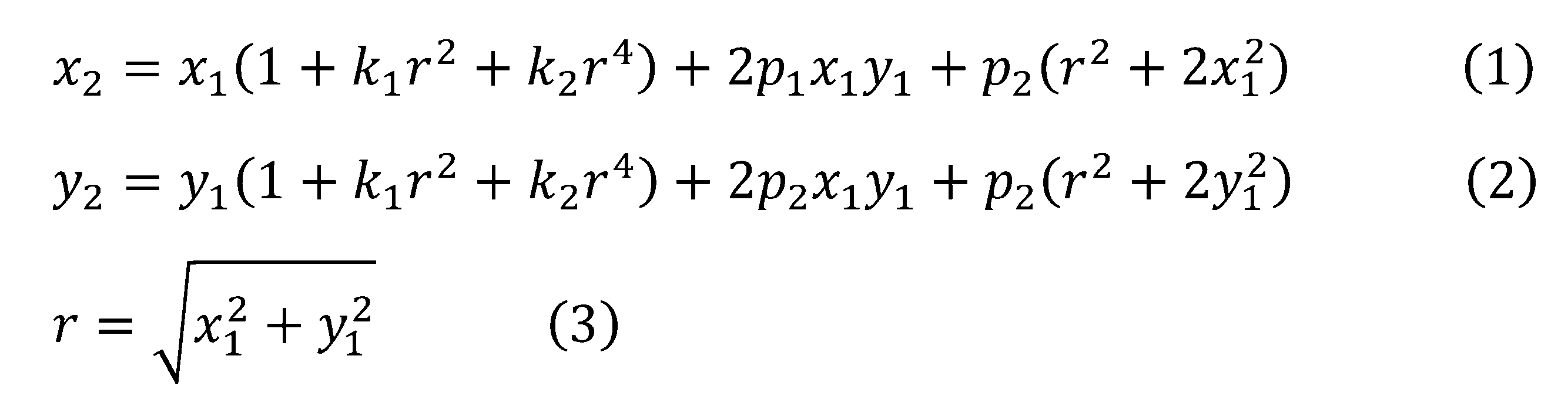
- the signal processor 16 can realize distortion correction of the image information or the event detection information, for example, based on the following equation:
- (x 1 , y 1 ) are image coordinates after distortion correction
- (x 2 , y 2 ) are image coordinates before distortion correction
- (x 1 , y 1 ) may be coordinates in a coordinate system that is further transformed from world coordinates to camera coordinates using external parameters and then transformed to image coordinates using internal parameters.
- k 1 , k 2 are distortion coefficients in the radial direction of the lens
- p 1 , p 2 are distortion coefficients in the circumferential direction of the lens.
- the distortion may be barrel distortion, pincushion distortion, or a combination of these.
- the signal processing unit 16 performs appropriate signal processing using the distortion-corrected or uncorrected image information and the distortion-corrected or uncorrected event detection information.
- This signal processing may be, for example, processing using an SNN (Spiking Neural Network). Processing is not limited to using an SNN, and the signal processing unit 16 can perform appropriate processing of the image information using the distortion-corrected event detection information as necessary.
- the solid-state imaging device 1 can realize signal processing including distortion correction of the acquired event detection information as necessary. By correcting the distortion of the event detection information, it becomes possible to realize signal processing and image processing in which event detection information using the same coordinate system is added to the coordinate information in the image information.
- FIG. 6 is a flowchart showing the processing of the solid-state imaging device 1 according to one embodiment. This flowchart shows the flow when float arithmetic (floating point arithmetic) is possible in processing the event detection information. The following flowchart can also be used when fixed-point processing is possible.
- the solid-state imaging device 1 obtains information about reflected light, transmitted light, or emitted light from various objects in the imaging area in the imaging section 12 using a first pixel 121 and a second pixel 122 in the pixel array 120 (S100).
- the signal processing unit 16 appropriately pre-processes the acquired output from the first pixel 121 (S102). As described above, this pre-processing may include analog to digital conversion, defect correction, demosaicing, color matrix processing, etc. Note that some of the processing may be performed by the imaging unit 12, which then transmits the processed data to the signal processing unit 16.
- the signal processing unit 16 determines whether the setting specified by the user or by the solid-state imaging device 1 is for distortion correction or for distortion not correction (S104).
- the setting for distortion correction may be specified by the user, or may be determined and specified by the solid-state imaging device 1 based on information of the video signal, etc.
- the signal processing unit 16 performs distortion correction on the image obtained from the luminance information by performing distortion correction on the preprocessed image information (S106).
- the distortion correction is performed, for example, based on the above equations (1) to (3).
- the signal processing unit 16 appropriately pre-processes the acquired output from the second pixel 122 (S108). This pre-processing may include, for example, converting the information acquired in an arbiter format into a per-frame event grid.
- the signal processing unit 16 determines whether the setting specified by the user or by the solid-state imaging device 1 is for performing distortion correction or for not performing distortion correction (S110).
- the setting for performing distortion correction may be specified by the user, or may be determined and specified by the solid-state imaging device 1 based on information on the video signal, etc. Furthermore, when image information is to be distortion corrected, the signal processing unit 16 may also be set to automatically perform distortion correction on the event detection signal.
- the signal processing unit 16 performs distortion correction on the event detection information obtained from the brightness change information by performing distortion correction on the preprocessed event detection signal (S112).
- FIG. 7 is a flowchart showing an example of the processing of S112 described above according to one embodiment.
- the signal processing unit 16 determines whether or not to resize the event detection information (S1120).
- the decision to resize may be set in advance, in which case, depending on the setting, the following process of S1122 or S1126 may be executed by software or hardware implementation without going through the process of S1120.
- the signal processing unit 16 executes a process of adjusting the resolution of the data preprocessed as event detection information so that it matches the coordinates in the image information.
- a general method can be used for the resolution conversion. This resolution conversion allows the event detection information to be placed in the same coordinate system as the image information, at the same scale.
- the event detection information may be expressed as floating point.
- the signal processing unit 16 performs distortion correction on the resolution-converted event detection information (S1124).
- the signal processing unit 16 can perform this distortion correction according to equations (1) to (3) that have coefficients in common with the image information.
- the signal processing unit 16 can use the high-resolution event detection information to obtain distortion-corrected event detection information in the same coordinate system as the image information.
- the signal processing unit 16 can convert the event detection information into the resolution of the image information and perform distortion correction on the converted event detection information.
- the signal processing unit 16 performs distortion correction on the event detection information taking into account scaling (S1126). For example, the signal processing unit 16 can apply equations (1) to (3) to the image coordinates before distortion correction ( x'2 , y'2 ) scaled by the following conversion equation ( x2 , y2 ). Note that the distortion coefficients can be the same as those used for distortion correction of image information, as described above.
- the event detection information may be expressed as floating point.
- the signal processing unit 16 can perform distortion correction that takes into account scaling based on the difference between the resolution of the event detection information and the resolution of the image information.
- N in equations (4) and (5) can be determined based on the predetermined ratio described above.
- the signal processing unit 16 can perform any post-processing based on the acquired image information and event detection information (S114).
- the post-processing may be, for example, the above-mentioned SNN processing, processing using other trained models, or any processing that does not use trained models.
- the coordinates of the event detection information can be matched with the coordinates of the image information based on this distortion-corrected information, and processing using various trained models such as SNNs, tracking processing, etc. can be realized.
- the signal processing unit 16 can appropriately output the data after performing post-processing (S116). This output may be in the form of outputting the data to the outside of the solid-state imaging device 1 via the input/output I/F 18, or may be in the form of storing the data in the memory unit 14.
- the signal processing unit 16 can set a region of interest on the image, for example, by processing such as object detection in the signal processing unit 16, or by user specification.
- the signal processing unit 16 can realize event detection for this region of interest.
- FIG. 8 is a flowchart showing the processing of the solid-state imaging device 1 according to one embodiment.
- the signal processing unit 16 sets a region of interest in the image information (S200).
- the signal processing unit 16 may set a region specified by the user via the input/output I/F 18 as the region of interest.
- the signal processing unit 16 may set a region including an object specified by the user via the input/output I/F 18 as the region of interest.
- the signal processing unit 16 may also detect an object by any processing and set a region of interest based on the detection result.
- the signal processing unit 16 can obtain the region of interest in the coordinate system of the undistorted event detection information by performing inverse distortion correction on the region of interest in the image information (S202). At the timing of this inverse distortion correction, the signal processing unit 16 can also convert coordinates taking into account the resizing and scaling described in the second embodiment above, if necessary.
- the signal processing unit 16 obtains the region of interest in the event detection information (S204).
- the solid-state imaging device 1 can also convert a region of interest in a distortion-corrected image into a region of interest in event detection information that has not been distortion-corrected.
- FIG. 9 is a diagram showing an example of region of interest setting according to one embodiment.
- the solid-state imaging device 1 acquires video information or time-series continuous image information including a person as a target.
- the signal processing unit 16 automatically extracts an eye area from the distortion-corrected image and sets the region of interest ROIi.
- the user may specify an arbitrary position within the image, and the signal processing unit 16 may set the region of interest ROIi based on this specification.
- the signal processing unit 16 performs an inverse distortion transformation on the region of interest ROIi to obtain information on the region of interest ROIe in the coordinate system of the uncorrected event detection information.
- the region of interest ROIe is shown as a rectangle in the figure, this is not limited to this, and if there is a barrel-shaped or pincushion-shaped distortion or a combination of these, it is also possible to obtain information on the region of interest ROIe according to the shape of this distortion.
- the signal processing unit 16 can perform tracking of an object contained within a region of interest ROIi set in an image by acquiring event information in the region of interest ROIe and the surroundings of the region of interest ROIe in the coordinate system (not distortion corrected) of the event detection information.
- FIG. 10 is a flowchart showing an example of processing in the above tracking example.
- the signal processing unit 16 judges whether or not to perform tracking (S300). Whether or not to perform tracking may be specified by the user, or may be specified automatically by the solid-state imaging device 1. If tracking is not to be performed (S300: NO), the following processing may not be performed, or the device may transition to a standby state for the judgment of S300.
- the signal processing unit 16 acquires the region of interest at the coordinates of the event detection information that has not been subjected to distortion correction by the processes of S200 to S204 in FIG. 8.
- the signal processing unit 16 starts tracking using the event detection information (S302). In the following process, the signal processing unit 16 performs tracking for the region of interest ROIe in FIG. 9, for example.
- the signal processing unit 16 detects event information in and around the region of interest ROIe, and calculates the amount of movement from the previous frame to the current frame from the change in brightness information in the region of interest ROIe (S304). For example, the signal processing unit 16 tracks the region of interest ROIe from the event detection information in the lower left of Figure 9 to the event detection information in the lower right, and obtains the amount of movement or the coordinates of the destination (with distortion).
- the signal processing unit 16 sets the same region of interest as the region of interest ROIe obtained from the event detection information (if resizing or scaling has been performed, the same region taking these into consideration) as the region of interest for the image information before distortion correction, and performs tracking in the image by performing distortion correction on the image information including this region of interest (S306).
- the signal processing unit 16 can obtain the region of interest ROIi in the distortion-corrected coordinate system as shown in the upper right of Figure 9.
- the signal processing unit 16 continues the processes of S304 and S306 until tracking is terminated (S308: NO).
- the end of tracking can be determined depending on the situation, for example, when shooting is completed, when the user issues a command to terminate tracking, etc.
- event detection information can be acquired faster than acquiring luminance information (image information), and the calculation costs can be lower than those of luminance information. This makes it possible to achieve processing related to event detection, such as tracking, that is faster than processing using image information.
- the solid-state imaging device 1 can implement the above, for example, in autofocus processing using eye tracking. That is, the solid-state imaging device 1 can, for example, perform eye tracking based on event detection information, and acquire an image in which the optical system is controlled so as to focus on a region of interest acquired in the image information. Furthermore, without being limited to this, it is possible to acquire event detection information at a higher speed and realize processing for applying it to frames of image information.
- the process after acquiring the event detection information may not support floating-point arithmetic, such as inputting the results to the SNN.
- a form can be used that does not output the data acquired after distortion correction in floating-point format.
- the signal processing unit 16 controls the result after distortion correction so that it is not a floating point and outputs it.
- the signal processing unit 16 may select the (x, y) coordinates of the event detection information that are the closest to the coordinates of the event detection information, obtain the converted value of the event detection information at the coordinates (x, y), and compare this obtained value with a threshold value to obtain the event detection result at the coordinates (x, y).
- the signal processing unit 16 may determine that a positive event has occurred if the event detection value at the coordinates (x, y) after distortion correction is equal to or greater than a predetermined positive threshold, that a negative event has occurred if the value is equal to or less than a predetermined negative threshold, and that no event has occurred otherwise.
- the signal processing unit 16 can also output this result as a 1.5 bit result.
- the signal processing unit 16 can convert the results obtained in floating point to 1.5-bit data and output it. By converting the data in this way, it becomes possible to use the output data in its original form.
- a hybrid pixel configuration has been described in which a first pixel 121 and a second pixel 122 are arranged in the same pixel array 120.
- the embodiments of the present disclosure are not limited to this, and may be a so-called sensor fusion configuration.
- FIG. 11 is a block diagram showing a schematic diagram of a solid-state imaging device according to one embodiment.
- the solid-state imaging device 1 includes a first optical system 10A and a second optical system 10B as optical systems, and a first imaging section 12A and a second imaging section 12B as imaging sections.
- the first imaging unit 12A has a first pixel array in which first pixels 121 that acquire luminance information are arranged in a two-dimensional array.
- the first optical system 10A is configured to focus light on the first pixel array.
- the second imaging unit 12B has a second pixel array in which second pixels 121 that acquire information on changes in luminance are arranged in a two-dimensional array.
- the second optical system 10B is configured to focus light on the second pixel array.
- the signal processing unit 16 can, for example, perform processing to adapt the event detection information acquired in the second pixel array to the image information acquired in the first pixel array. Through this processing, the signal processing unit 16 can realize processing to match the coordinates of the event detection information with the coordinates of the image information before or after distortion correction.
- the solid-state imaging device 1 is not limited to the form shown in FIG. 11.
- the solid-state imaging device 1 may have a form having one optical system for the first imaging section 12A and the second imaging section 12B.
- the distortion coefficients may be set for each pixel array as needed.
- the solid-state imaging device 1 may be configured to include, for example, a first signal processing unit that processes signals from the first imaging unit 12A, and a second signal processing unit that processes signals from the second imaging unit 12B.
- the first signal processing unit and the second signal processing unit may be configured to be able to share data as necessary.
- each imaging unit may be formed on a separate semiconductor chip, or may be formed on the same semiconductor chip.
- the solid-state imaging device 1 can realize deblur processing, optical flow processing, motion blur removal processing, etc., based on distortion-corrected image information and distortion-corrected event detection information, for example.
- the solid-state imaging device 1 can perform any image processing on image information using the event detection information on which distortion correction has been performed, in addition to the blur correction and tracking processing described above. As another non-limiting example, the solid-state imaging device 1 can also achieve a high frame rate for image information on which distortion correction has been performed.
- FIG. 12 shows an example of an implementation of a chip 20 in a solid-state imaging device 1.
- the chip 20 has a pixel array region 200, a memory circuit region 202, and a processing circuit region 204 on the same semiconductor substrate 30.
- a single semiconductor substrate 30 may have the pixel array region 200, the memory circuit region 202, and the processing circuit region 204.
- Each part is connected by an appropriate conductor or the like.
- the pixel array region 200 is the region in which the pixel array 120 is disposed.
- the memory circuit region 202 is the region in which at least a portion of the memory unit 14 is disposed.
- the processing circuit region 204 is the region in which at least the signal processing unit 16 is disposed.
- the chip 20 may be implemented on different semiconductor layers, a first semiconductor layer 31 and a second semiconductor layer 32.
- the first semiconductor layer 31 includes a pixel array region 200
- the second semiconductor layer 32 includes a memory circuit region 202 and a processing circuit region 204.
- the first semiconductor layer 31 and the second semiconductor layer 32 are stacked to form and operate as an integrated semiconductor device.
- the first semiconductor layer 31 is disposed closer to the optical system 100 than the second semiconductor layer 32, and light passing through the optical system 100 is received by the first semiconductor layer 31, and a signal is output to the second semiconductor layer 32.
- the chip 20 may be implemented on different semiconductor layers, a first semiconductor layer 31, a second semiconductor layer 32, and a third semiconductor layer 33.
- the first semiconductor layer 31 includes a pixel array region 200
- the second semiconductor layer 32 includes a memory circuit region 202
- the third semiconductor layer 33 includes a processing circuit region 204.
- the first semiconductor layer 31, the second semiconductor layer 32, and the third semiconductor layer 33 are stacked to form and operate as an integrated semiconductor device.
- the first semiconductor layer 31 is disposed closest to the optical system 100, light passing through the optical system 100 is received by the first semiconductor layer 31, and a signal is output to at least one of the second semiconductor layer 32 and the third semiconductor layer 33.
- the semiconductor layers may be cut out from a wafer, diced, and then stacked and bonded together using the CoC (Chip on Chip) method.
- the CoW (Chip on Wafer) method may be used, in which one of the layers is cut out, diced, and then bonded to the wafer.
- the WoW (Wafer on Wafer) method may be used, in which each wafer is bonded together and then diced.
- each semiconductor layer can be bonded together using non-limiting examples such as via holes, microbumps, micropads, plasma bonding, etc.
- each semiconductor layer is appropriately electrically connected and formed so as to be capable of transmitting and receiving signals.
- the technology disclosed herein can be applied to a variety of products.
- the technology disclosed herein may be realized as a device mounted on any type of moving object, such as an automobile, electric vehicle, hybrid electric vehicle, motorcycle, bicycle, personal mobility, airplane, drone, ship, robot, construction machine, agricultural machine (tractor), etc.
- FIG. 15 is a block diagram showing a schematic configuration example of a vehicle control system 7000, which is an example of a mobile control system to which the technology disclosed herein can be applied.
- the vehicle control system 7000 includes a plurality of electronic control units connected via a communication network 7010.
- the vehicle control system 7000 includes a drive system control unit 7100, a body system control unit 7200, a battery control unit 7300, an outside vehicle information detection unit 7400, an inside vehicle information detection unit 7500, and an integrated control unit 7600.
- the communication network 7010 connecting these multiple control units may be, for example, an in-vehicle communication network conforming to any standard such as CAN (Controller Area Network), LIN (Local Interconnect Network), LAN (Local Area Network), or FlexRay (registered trademark).
- CAN Controller Area Network
- LIN Local Interconnect Network
- LAN Local Area Network
- FlexRay registered trademark
- Each control unit includes a microcomputer that performs arithmetic processing according to various programs, a storage unit that stores the programs executed by the microcomputer or parameters used in various calculations, and a drive circuit that drives various devices to be controlled.
- Each control unit includes a network I/F for communicating with other control units via a communication network 7010, and a communication I/F for communicating with devices or sensors inside and outside the vehicle by wired or wireless communication.
- the functional configuration of the integrated control unit 7600 includes a microcomputer 7610, a general-purpose communication I/F 7620, a dedicated communication I/F 7630, a positioning unit 7640, a beacon receiving unit 7650, an in-vehicle device I/F 7660, an audio/image output unit 7670, an in-vehicle network I/F 7680, and a storage unit 7690.
- Other control units also include a microcomputer, a communication I/F, a storage unit, and the like.
- the drive system control unit 7100 controls the operation of devices related to the drive system of the vehicle according to various programs.
- the drive system control unit 7100 functions as a control device for a drive force generating device for generating a drive force for the vehicle, such as an internal combustion engine or a drive motor, a drive force transmission mechanism for transmitting the drive force to the wheels, a steering mechanism for adjusting the steering angle of the vehicle, and a braking device for generating a braking force for the vehicle.
- the drive system control unit 7100 may also function as a control device such as an ABS (Antilock Brake System) or ESC (Electronic Stability Control).
- the drive system control unit 7100 is connected to a vehicle state detection unit 7110.
- the vehicle state detection unit 7110 includes at least one of the following: a gyro sensor that detects the angular velocity of the axial rotational motion of the vehicle body, an acceleration sensor that detects the acceleration of the vehicle, or a sensor for detecting the amount of operation of the accelerator pedal, the amount of operation of the brake pedal, the steering angle of the steering wheel, the engine speed, or the rotation speed of the wheels.
- the drive system control unit 7100 performs arithmetic processing using the signal input from the vehicle state detection unit 7110, and controls the internal combustion engine, the drive motor, the electric power steering device, the brake device, etc.
- the body system control unit 7200 controls the operation of various devices installed in the vehicle body according to various programs.
- the body system control unit 7200 functions as a control device for a keyless entry system, a smart key system, a power window device, or various lamps such as headlamps, tail lamps, brake lamps, turn signals, and fog lamps.
- radio waves or signals from various switches transmitted from a portable device that replaces a key can be input to the body system control unit 7200.
- the body system control unit 7200 accepts the input of these radio waves or signals and controls the vehicle's door lock device, power window device, lamps, etc.
- the battery control unit 7300 controls the secondary battery 7310, which is the power supply source for the drive motor, according to various programs. For example, information such as the battery temperature, battery output voltage, or remaining capacity of the battery is input to the battery control unit 7300 from a battery device equipped with the secondary battery 7310. The battery control unit 7300 performs calculations using these signals, and controls the temperature regulation of the secondary battery 7310 or a cooling device or the like equipped in the battery device.
- the outside vehicle information detection unit 7400 detects information outside the vehicle equipped with the vehicle control system 7000.
- the imaging unit 7410 and the outside vehicle information detection unit 7420 is connected to the outside vehicle information detection unit 7400.
- the imaging unit 7410 includes at least one of a ToF (Time Of Flight) camera, a stereo camera, a monocular camera, an infrared camera, and other cameras.
- the outside vehicle information detection unit 7420 includes at least one of an environmental sensor for detecting the current weather or climate, or a surrounding information detection sensor for detecting other vehicles, obstacles, pedestrians, etc., around the vehicle equipped with the vehicle control system 7000.
- the environmental sensor may be, for example, at least one of a raindrop sensor that detects rain, a fog sensor that detects fog, a sunshine sensor that detects the level of sunlight, and a snow sensor that detects snowfall.
- the surrounding information detection sensor may be at least one of an ultrasonic sensor, a radar device, and a LIDAR (Light Detection and Ranging, Laser Imaging Detection and Ranging) device.
- the imaging unit 7410 and the outside vehicle information detection unit 7420 may each be provided as an independent sensor or device, or may be provided as a device in which multiple sensors or devices are integrated.
- FIG. 16 shows an example of the installation positions of the imaging unit 7410 and the outside vehicle information detection unit 7420.
- the imaging units 7910, 7912, 7914, 7916, and 7918 are provided, for example, at least one of the front nose, side mirrors, rear bumper, back door, and the upper part of the windshield inside the vehicle cabin of the vehicle 7900.
- the imaging unit 7910 provided on the front nose and the imaging unit 7918 provided on the upper part of the windshield inside the vehicle cabin mainly obtain images of the front of the vehicle 7900.
- the imaging units 7912 and 7914 provided on the side mirrors mainly obtain images of the sides of the vehicle 7900.
- the imaging unit 7916 provided on the rear bumper or back door mainly obtains images of the rear of the vehicle 7900.
- the imaging unit 7918, which is installed on the top of the windshield inside the vehicle is primarily used to detect preceding vehicles, pedestrians, obstacles, traffic signals, traffic signs, lanes, etc.
- FIG. 16 shows an example of the imaging ranges of each of the imaging units 7910, 7912, 7914, and 7916.
- Imaging range a indicates the imaging range of the imaging unit 7910 provided on the front nose
- imaging ranges b and c indicate the imaging ranges of the imaging units 7912 and 7914 provided on the side mirrors, respectively
- imaging range d indicates the imaging range of the imaging unit 7916 provided on the rear bumper or back door.
- an overhead image of the vehicle 7900 viewed from above is obtained by superimposing the image data captured by the imaging units 7910, 7912, 7914, and 7916.
- External information detection units 7920, 7922, 7924, 7926, 7928, and 7930 provided on the front, rear, sides, corners, and upper part of the windshield inside the vehicle 7900 may be, for example, ultrasonic sensors or radar devices.
- External information detection units 7920, 7926, and 7930 provided on the front nose, rear bumper, back door, and upper part of the windshield inside the vehicle 7900 may be, for example, LIDAR devices. These external information detection units 7920 to 7930 are mainly used to detect preceding vehicles, pedestrians, obstacles, etc.
- the outside-vehicle information detection unit 7400 causes the imaging unit 7410 to capture an image outside the vehicle, and receives the captured image data.
- the outside-vehicle information detection unit 7400 also receives detection information from the connected outside-vehicle information detection unit 7420. If the outside-vehicle information detection unit 7420 is an ultrasonic sensor, a radar device, or a LIDAR device, the outside-vehicle information detection unit 7400 transmits ultrasonic waves or electromagnetic waves, and receives information on the received reflected waves.
- the outside-vehicle information detection unit 7400 may perform object detection processing or distance detection processing for people, cars, obstacles, signs, or characters on the road surface, based on the received information.
- the outside vehicle information detection unit 7400 may also perform image recognition processing or distance detection processing to recognize people, cars, obstacles, signs, or characters on the road surface based on the received image data.
- the outside vehicle information detection unit 7400 may perform processing such as distortion correction or alignment on the received image data, and may also generate an overhead image or a panoramic image by synthesizing image data captured by different imaging units 7410.
- the outside vehicle information detection unit 7400 may also perform viewpoint conversion processing using image data captured by different imaging units 7410.
- the in-vehicle information detection unit 7500 detects information inside the vehicle.
- a driver state detection unit 7510 that detects the state of the driver is connected to the in-vehicle information detection unit 7500.
- the driver state detection unit 7510 may include a camera that captures an image of the driver, a biosensor that detects the driver's biometric information, or a microphone that collects sound inside the vehicle.
- the biosensor is provided, for example, on the seat or steering wheel, and detects the biometric information of a passenger sitting in the seat or a driver gripping the steering wheel.
- the in-vehicle information detection unit 7500 may calculate the degree of fatigue or concentration of the driver based on the detection information input from the driver state detection unit 7510, or may determine whether the driver is dozing off.
- the in-vehicle information detection unit 7500 may perform processing such as noise canceling on the collected sound signal.
- the integrated control unit 7600 controls the overall operation of the vehicle control system 7000 according to various programs.
- the input unit 7800 is connected to the integrated control unit 7600.
- the input unit 7800 is realized by a device that can be operated by the passenger, such as a touch panel, a button, a microphone, a switch, or a lever. Data obtained by voice recognition of a voice input by a microphone may be input to the integrated control unit 7600.
- the input unit 7800 may be, for example, a remote control device using infrared or other radio waves, or an externally connected device such as a mobile phone or a PDA (Personal Digital Assistant) that supports the operation of the vehicle control system 7000.
- PDA Personal Digital Assistant
- the input unit 7800 may be, for example, a camera, in which case the passenger can input information by gestures. Alternatively, data obtained by detecting the movement of a wearable device worn by the passenger may be input. Furthermore, the input unit 7800 may include, for example, an input control circuit that generates an input signal based on information input by a passenger or the like using the input unit 7800 and outputs the signal to the integrated control unit 7600. The passenger or the like operates the input unit 7800 to input various data to the vehicle control system 7000 and to instruct processing operations.
- the memory unit 7690 may include a ROM (Read Only Memory) that stores various programs executed by the microcomputer, and a RAM (Random Access Memory) that stores various parameters, calculation results, sensor values, etc.
- the memory unit 7690 may also be realized by a magnetic memory device such as a HDD (Hard Disc Drive), a semiconductor memory device, an optical memory device, or a magneto-optical memory device, etc.
- the general-purpose communication I/F 7620 is a general-purpose communication I/F that mediates communication between various devices present in the external environment 7750.
- the general-purpose communication I/F 7620 may implement cellular communication protocols such as GSM (registered trademark) (Global System of Mobile communications), WiMAX (registered trademark), LTE (registered trademark) (Long Term Evolution) or LTE-A (LTE-Advanced), or other wireless communication protocols such as wireless LAN (also called Wi-Fi (registered trademark)) and Bluetooth (registered trademark).
- GSM Global System of Mobile communications
- WiMAX registered trademark
- LTE registered trademark
- LTE-A Long Term Evolution
- Bluetooth registered trademark
- the general-purpose communication I/F 7620 may connect to devices (e.g., application servers or control servers) present on an external network (e.g., the Internet, a cloud network, or an operator-specific network) via, for example, a base station or an access point.
- the general-purpose communication I/F 7620 may connect to a terminal located near the vehicle (e.g., a driver's, pedestrian's, or store's terminal, or an MTC (Machine Type Communication) terminal) using, for example, P2P (Peer To Peer) technology.
- P2P Peer To Peer
- the dedicated communication I/F 7630 is a communication I/F that supports a communication protocol developed for use in a vehicle.
- the dedicated communication I/F 7630 may implement a standard protocol such as WAVE (Wireless Access in Vehicle Environment), DSRC (Dedicated Short Range Communications), or a cellular communication protocol, which is a combination of the lower layer IEEE 802.11p and the higher layer IEEE 1609.
- the dedicated communication I/F 7630 typically performs V2X communication, which is a concept that includes one or more of vehicle-to-vehicle communication, vehicle-to-infrastructure communication, vehicle-to-home communication, and vehicle-to-pedestrian communication.
- the positioning unit 7640 performs positioning by receiving, for example, GNSS signals from GNSS (Global Navigation Satellite System) satellites (for example, GPS signals from GPS (Global Positioning System) satellites), and generates position information including the latitude, longitude, and altitude of the vehicle.
- GNSS Global Navigation Satellite System
- GPS Global Positioning System
- the positioning unit 7640 may determine the current position by exchanging signals with a wireless access point, or may obtain position information from a terminal such as a mobile phone, PHS, or smartphone that has a positioning function.
- the beacon receiver 7650 receives, for example, radio waves or electromagnetic waves transmitted from radio stations installed on the road, and acquires information such as the current location, congestion, road closures, and travel time.
- the functions of the beacon receiver 7650 may be included in the dedicated communication I/F 7630 described above.
- the in-vehicle device I/F 7660 is a communication interface that mediates the connection between the microcomputer 7610 and various in-vehicle devices 7760 present in the vehicle.
- the in-vehicle device I/F 7660 may establish a wireless connection using a wireless communication protocol such as wireless LAN, Bluetooth (registered trademark), NFC (Near Field Communication), or WUSB (Wireless USB).
- the in-vehicle device I/F 7660 may also establish a wired connection such as USB (Universal Serial Bus), HDMI (High-Definition Multimedia Interface), or MHL (Mobile High-definition Link) via a connection terminal (and a cable, if necessary) not shown.
- USB Universal Serial Bus
- HDMI High-Definition Multimedia Interface
- MHL Mobile High-definition Link
- the in-vehicle device 7760 may include, for example, at least one of a mobile device or wearable device owned by a passenger, or an information device carried into or attached to the vehicle.
- the in-vehicle device 7760 may also include a navigation device that searches for a route to an arbitrary destination.
- the in-vehicle device I/F 7660 exchanges control signals or data signals with these in-vehicle devices 7760.
- the in-vehicle network I/F 7680 is an interface that mediates communication between the microcomputer 7610 and the communication network 7010.
- the in-vehicle network I/F 7680 transmits and receives signals in accordance with a specific protocol supported by the communication network 7010.
- the microcomputer 7610 of the integrated control unit 7600 controls the vehicle control system 7000 according to various programs based on information acquired through at least one of the general-purpose communication I/F 7620, the dedicated communication I/F 7630, the positioning unit 7640, the beacon receiving unit 7650, the in-vehicle device I/F 7660, and the in-vehicle network I/F 7680.
- the microcomputer 7610 may calculate the control target value of the driving force generating device, the steering mechanism, or the braking device based on the acquired information inside and outside the vehicle, and output a control command to the drive system control unit 7100.
- the microcomputer 7610 may perform cooperative control for the purpose of realizing the functions of an ADAS (Advanced Driver Assistance System), including vehicle collision avoidance or impact mitigation, following driving based on the distance between vehicles, vehicle speed maintenance driving, vehicle collision warning, vehicle lane departure warning, etc.
- ADAS Advanced Driver Assistance System
- the microcomputer 7610 may control the driving force generating device, steering mechanism, braking device, etc. based on the acquired information about the surroundings of the vehicle, thereby performing cooperative control for the purpose of automatic driving, which allows the vehicle to travel autonomously without relying on the driver's operation.
- the microcomputer 7610 may generate three-dimensional distance information between the vehicle and objects such as surrounding structures and people based on information acquired via at least one of the general-purpose communication I/F 7620, the dedicated communication I/F 7630, the positioning unit 7640, the beacon receiving unit 7650, the in-vehicle equipment I/F 7660, and the in-vehicle network I/F 7680, and may create local map information including information about the surroundings of the vehicle's current position.
- the microcomputer 7610 may also predict dangers such as vehicle collisions, the approach of pedestrians, or entry into closed roads based on the acquired information, and generate warning signals.
- the warning signals may be, for example, signals for generating warning sounds or turning on warning lights.
- the audio/image output unit 7670 transmits at least one of audio and image output signals to an output device capable of visually or audibly notifying the vehicle occupants or the outside of the vehicle of information.
- an audio speaker 7710, a display unit 7720, and an instrument panel 7730 are illustrated as output devices.
- the display unit 7720 may include, for example, at least one of an on-board display and a head-up display.
- the display unit 7720 may have an AR (Augmented Reality) display function.
- the output device may be other devices such as headphones, wearable devices such as glasses-type displays worn by the occupants, projectors, or lamps other than these devices.
- the display device visually displays the results obtained by various processes performed by the microcomputer 7610 or information received from other control units in various formats such as text, images, tables, graphs, etc. Also, if the output device is an audio output device, the audio output device converts an audio signal consisting of reproduced voice data or acoustic data, etc., into an analog signal and outputs it audibly.
- At least two control units connected via the communication network 7010 may be integrated into one control unit.
- each control unit may be composed of multiple control units.
- the vehicle control system 7000 may include another control unit not shown.
- some or all of the functions performed by any control unit may be provided by another control unit.
- a specified calculation process may be performed by any control unit.
- a sensor or device connected to any control unit may be connected to another control unit, and multiple control units may transmit and receive detection information to each other via the communication network 7010.
- a computer program for implementing each function of the solid-state imaging device 1 according to this embodiment described with reference to Figures 1 to 14, particularly the signal processing unit 16, can be implemented in any of the control units, etc.
- a computer-readable recording medium on which such a computer program is stored can also be provided.
- the recording medium is, for example, a magnetic disk, an optical disk, a magneto-optical disk, a flash memory, etc.
- the above computer program may be distributed, for example, via a network, without using a recording medium.
- An optical system A first pixel that acquires image information based on luminance information via the optical system; A second pixel that acquires event detection information based on a change in luminance information via the optical system.
- a solid-state imaging device comprising:
- the one or more pixel arrays are formed from a single pixel array;
- the second pixels are arranged in a predetermined region of the pixel array at a predetermined ratio to the first pixels.
- the predetermined area is the entire area of the pixel array.
- the second pixels are arranged at equal intervals so as to cover the entire area of the predetermined region.
- the second pixel detects an event in an arbiter manner.
- a solid-state imaging device according to any one of (1) to (4).
- the signal processing circuit performs distortion correction of the image information.
- a solid-state imaging device according to any one of (1) to (6).
- the signal processing circuit includes: converting the event detection information into a resolution of the image information; performing distortion correction of the converted event detection information; A solid-state imaging device according to (7).
- the signal processing circuit includes: performing distortion correction of the event detection information based on a difference between a resolution of the event detection information and a resolution of the image information; A solid-state imaging device according to (7).
- the signal processing circuit includes: Setting a region of interest based on the image information; obtaining the event detection information corresponding to the region of interest; A solid-state imaging device according to any one of (1) to (9).
- the signal processing circuit includes: performing tracking based on the distortion-corrected event detection information corresponding to the region of interest; A solid-state imaging device according to (10).
- the signal processing circuit includes: comparing a value obtained by correcting the distortion of the event detection information with a threshold value for the coordinates after the distortion correction, thereby acquiring the event detection information at the coordinates after the distortion correction; A solid-state imaging device according to any one of (1) to (11).
- the one or more pixel arrays a first pixel array in which the first pixels are arranged in a two-dimensional array; a second pixel array, the second pixels being arranged in a two-dimensional array and configured to acquire the event detection information of the same target as that of the first pixel array; formed from A solid-state imaging device according to (1).
- the optical system includes: a first optical system that focuses light onto the first pixel array; a second optical system that focuses light onto the second pixel array; Equipped with A solid-state imaging device according to (14).
- the signal processing circuit includes: a first signal processing circuit that processes a signal output from the first pixel; a second signal processing circuit that processes a signal output from the second pixel; Equipped with A solid-state imaging device according to any one of (1) to (15).
- the signal processing circuit includes: performing image processing based on the distortion-corrected image information and the distortion-corrected event detection information; A solid-state imaging device according to any one of (1) to (16).
- the signal processing circuit includes: performing a deblur process based on the distortion-corrected image information and the distortion-corrected event detection information; A solid-state imaging device according to (17).
- the signal processing circuit includes: performing a frame rate increasing process based on the distortion-corrected image information and the distortion-corrected event detection information; A solid-state imaging device according to (17) or (18).
- the signal processing circuit includes: performing a tracking process based on the distortion-corrected image information and the distortion-corrected event detection information; A solid-state imaging device according to any one of (1) to (19).
- 1 Solid-state imaging device
- 10 Optical system
- 12 Imaging unit
- 120 pixel array
- 121 1st pixel
- 122 2nd pixel
- 124 horizontal drive circuit
- 126 vertical drive circuit
- 128 Processing circuit
- 14 memory unit
- 16 Signal processing section
- 18 Input/Output Interface 20: Chip
- 200 pixel array area
- 202 memory circuit area
- 204 Processing circuit area
- 31 first semiconductor layer
- 32 second semiconductor layer
- 33 Third semiconductor layer
Landscapes
- Engineering & Computer Science (AREA)
- Multimedia (AREA)
- Signal Processing (AREA)
- Transforming Light Signals Into Electric Signals (AREA)
- Studio Devices (AREA)
Abstract
Description
第1画素は、前記光学系を介した輝度情報に基づいた画像情報を取得する。
第2画素は、前記光学系を介した輝度情報の変化に基づいたイベント検知情報を取得する。
1又は複数の画素アレイには、前記第1画素及び前記第2画素が2次元のアレイ状に備えられる。
信号処理回路は、前記第2画素が取得した前記イベント検知情報について、歪み補正をするか否かを選択して信号処理を実行する。
前記第2画素は、前記画素アレイ内の所定領域において、前記第1画素に対して所定割合で配置されていてもよい。
前記イベント検知情報を前記画像情報の解像度に変換してもよく、
変換した前記イベント検知情報の歪み補正を実行してもよい。
前記イベント検知情報の解像度と、前記画像情報の解像度と、の差異に基づいた前記イベント検知情報の歪み補正を実行してもよい。
前記画像情報に基づいて関心領域を設定してもよく、
前記関心領域に対応する前記イベント検知情報を取得してもよい。
前記関心領域に対応する歪み補正された前記イベント検知情報に基づいて、トラッキングを実行してもよい。
前記イベント検知情報を歪み補正した後の座標について、前記イベント検知情報を歪み補正した値としきい値を比較して、歪み補正をした後の前記座標におけるイベント検知情報を取得してもよい。
歪み補正をした後の前記座標におけるイベント検知情報を、 1.5 ビットの情報として格納してもよい。
前記第1画素が2次元のアレイ状に配置される、第1画素アレイと、
前記第2画素が2次元のアレイ状に配置され、前記第1画素アレイと同じ対象の前記イベント検知情報を取得する、第2画素アレイと、
から形成されてもよい。
前記第1画素アレイに光を集光する、第1光学系と、
前記第2画素アレイに光を集光する、第2光学系と、
を備えてもよい。
前記第1画素からの出力の信号処理をする、第1信号処理回路と、
前記第2画素からの出力の信号処理をする、第2信号処理回路と、
を備えてもよい。
歪み補正した前記画像情報及び歪み補正した前記イベント検知情報に基づいて、画像処理を実行してもよい。
歪み補正した前記画像情報及び歪み補正した前記イベント検知情報に基づいて、デブラー処理をしてもよい。
歪み補正した前記画像情報及び歪み補正した前記イベント検知情報に基づいて、高フレームレート化処理をしてもよい。
歪み補正した前記画像情報及び歪み補正した前記イベント検知情報に基づいて、トラッキング処理をしてもよい。
図1は、一実施形態に係る固体撮像装置を模式的に示すブロック図である。固体撮像装置 1 は、光学系 10 と、撮像部 12 と、記憶部 14 と、信号処理部 16 と、入出力インタフェース (以下、入出力I/F 18 と記載する。) と、を備える。固体撮像装置 1 は、少なくとも輝度情報から画像情報を取得する第1画素と、輝度情報の変化からイベント検知情報を取得する第2画素と、を備え、画像情報を取得するとともに、当該画像内におけるイベント検知情報を併せて取得する装置である。
上記の実施形態においては、固体撮像装置 1 の全体的な流れについて説明した。第2実施形態では、取得したイベント検知情報の歪み処理について詳しく説明する。

前述の実施形態においては、イベント検知情報を浮動小数点で表すことが可能である場合について説明したが、場合によっては浮動小数点で表すことができないこともある。また、浮動小数点で表示できる場合であっても、その後の処理においてイベント検知情報のフラグのみを取得したいこともある。このような場合には、第2実施形態のように浮動小数点で演算を実行すると、時間的及び演算的なコスト等の問題が発生する可能性がある。第3実施形態においては、このような浮動小数点演算を省略することが可能な実装について説明する。
前述したように、イベント検知情報を取得した後の処理がその結果をSNNの入力にする等、浮動小数点演算に対応しないことがある。このような場合には、歪み補正をした後に取得したデータを浮動小数点表示で出力しない形態を用いることができる。
前述のそれぞれの実施形態においては、同一の画素アレイ 120 に第1画素 121 と第2画素 122 とが配置されるハイブリッドな画素を備える形態について説明した。本開示における実施形態は、これに限定されるものではなく、所謂センサフュージョンの形態であってもよい。
前述の各実施形態では、例えば、トラッキングをする形態について説明したが、これに限定されるものではない。固体撮像装置 1 は、例えば、歪み補正した画像情報及び歪み補正したイベント検知情報に基づいて、デブラー処理、オプティカルフロー処理、モーションブラー除去処理等を実現することができる。
光学系と、
前記光学系を介した輝度情報に基づいた画像情報を取得する、第1画素と、
前記光学系を介した輝度情報の変化に基づいたイベント検知情報を取得する、第2画素と、
前記第1画素及び前記第2画素が2次元のアレイ状に備えられる、1又は複数の画素アレイと、
前記第2画素が取得した前記イベント検知情報について、歪み補正をするか否かを選択して信号処理を実行する、信号処理回路と、
を備える、固体撮像装置。
前記1又は複数の画素アレイは、1つの画素アレイから形成され、
前記第2画素は、前記画素アレイ内の所定領域において、前記第1画素に対して所定割合で配置されている、
(1)に記載の固体撮像装置。
前記所定領域は、前記画素アレイの全領域である、
(2)に記載の固体撮像装置。
前記第2画素は、前記所定領域の全域をカバーするように等間隔に配置されている、
(2)又は(3)に記載の固体撮像装置。
前記第2画素は、フレームごとにイベントを検知する、
(1)から(4)のいずれかに記載の固体撮像装置。
前記第2画素は、アービタ方式でイベントを検知する、
(1)から(4)のいずれかに記載の固体撮像装置。
前記信号処理回路は、前記画像情報の歪み補正を実行する、
(1)から(6)のいずれかに記載の固体撮像装置。
前記信号処理回路は、
前記イベント検知情報を前記画像情報の解像度に変換し、
変換した前記イベント検知情報の歪み補正を実行する、
(7)に記載の固体撮像装置。
前記信号処理回路は、
前記イベント検知情報の解像度と、前記画像情報の解像度と、の差異に基づいた前記イベント検知情報の歪み補正を実行する、
(7)に記載の固体撮像装置。
前記信号処理回路は、
前記画像情報に基づいて関心領域を設定し、
前記関心領域に対応する前記イベント検知情報を取得する、
(1)から(9)のいずれかに記載の固体撮像装置。
前記信号処理回路は、
前記関心領域に対応する歪み補正された前記イベント検知情報に基づいて、トラッキングを実行する、
(10)に記載の固体撮像装置。
前記信号処理回路は、
前記イベント検知情報を歪み補正した後の座標について、前記イベント検知情報を歪み補正した値としきい値を比較して、歪み補正をした後の前記座標におけるイベント検知情報を取得する、
(1)から(11)のいずれかに記載の固体撮像装置。
前記信号処理回路は、
歪み補正をした後の前記座標におけるイベント検知情報を、 1.5 ビットの情報として格納する、
(12)に記載の固体撮像装置。
前記1又は複数の画素アレイは、
前記第1画素が2次元のアレイ状に配置される、第1画素アレイと、
前記第2画素が2次元のアレイ状に配置され、前記第1画素アレイと同じ対象の前記イベント検知情報を取得する、第2画素アレイと、
から形成される、
(1)に記載の固体撮像装置。
前記光学系は、
前記第1画素アレイに光を集光する、第1光学系と、
前記第2画素アレイに光を集光する、第2光学系と、
を備える、
(14)に記載の固体撮像装置。
前記信号処理回路は、
前記第1画素からの出力の信号処理をする、第1信号処理回路と、
前記第2画素からの出力の信号処理をする、第2信号処理回路と、
を備える、
(1)から(15)のいずれかに記載の固体撮像装置。
前記信号処理回路は、
歪み補正した前記画像情報及び歪み補正した前記イベント検知情報に基づいて、画像処理を実行する、
(1)から(16)のいずれかに記載の固体撮像装置。
前記信号処理回路は、
歪み補正した前記画像情報及び歪み補正した前記イベント検知情報に基づいて、デブラー処理をする、
(17)に記載の固体撮像装置。
前記信号処理回路は、
歪み補正した前記画像情報及び歪み補正した前記イベント検知情報に基づいて、高フレームレート化処理をする、
(17)又は(18)に記載の固体撮像装置。
前記信号処理回路は、
歪み補正した前記画像情報及び歪み補正した前記イベント検知情報に基づいて、トラッキング処理をする、
(1)から(19)のいずれかに記載の固体撮像装置。
10: 光学系、
12: 撮像部、
120: 画素アレイ、
121: 第1画素、
122: 第2画素、
124: 水平駆動回路、
126: 垂直駆動回路、
128: 処理回路、
14: 記憶部、
16: 信号処理部、
18: 入出力I/F
20: チップ、
200: 画素アレイ領域、
202: 記憶回路領域、
204: 処理回路領域、
31: 第1半導体層、
32: 第2半導体層、
33: 第3半導体層
Claims (19)
- 光学系と、
前記光学系を介した輝度情報に基づいた画像情報を取得する、第1画素と、
前記光学系を介した輝度情報の変化に基づいたイベント検知情報を取得する、第2画素と、
前記第1画素及び前記第2画素が2次元のアレイ状に備えられる、1又は複数の画素アレイと、
前記第2画素が取得した前記イベント検知情報について、歪み補正をするか否かを選択して信号処理を実行する、信号処理回路と、
を備える、固体撮像装置。 - 前記1又は複数の画素アレイは、1つの画素アレイから形成され、
前記第2画素は、前記画素アレイ内の所定領域において、前記第1画素に対して所定割合で配置されている、
請求項1に記載の固体撮像装置。 - 前記所定領域は、前記画素アレイの全領域である、
請求項2に記載の固体撮像装置。 - 前記第2画素は、前記所定領域の全域をカバーするように等間隔に配置されている、
請求項2に記載の固体撮像装置。 - 前記第2画素は、フレームごとにイベントを検知する、
請求項1に記載の固体撮像装置。 - 前記第2画素は、アービタ方式でイベントを検知する、
請求項1に記載の固体撮像装置。 - 前記信号処理回路は、前記画像情報の歪み補正を実行する、
請求項1に記載の固体撮像装置。 - 前記信号処理回路は、
前記イベント検知情報を前記画像情報の解像度に変換し、
変換した前記イベント検知情報の歪み補正を実行する、
請求項7に記載の固体撮像装置。 - 前記信号処理回路は、
前記イベント検知情報の解像度と、前記画像情報の解像度と、の差異に基づいた前記イベント検知情報の歪み補正を実行する、
請求項7に記載の固体撮像装置。 - 前記信号処理回路は、
前記画像情報に基づいて関心領域を設定し、
前記関心領域に対応する前記イベント検知情報を取得する、
請求項1に記載の固体撮像装置。 - 前記信号処理回路は、
前記関心領域に対応する歪み補正された前記イベント検知情報に基づいて、トラッキングを実行する、
請求項10に記載の固体撮像装置。 - 前記信号処理回路は、
前記イベント検知情報を歪み補正した後の座標について、前記イベント検知情報を歪み補正した値としきい値を比較して、歪み補正をした後の前記座標におけるイベント検知情報を取得する、
請求項1に記載の固体撮像装置。 - 前記信号処理回路は、
歪み補正をした後の前記座標におけるイベント検知情報を、 1.5 ビットの情報として格納する、
請求項12に記載の固体撮像装置。 - 前記1又は複数の画素アレイは、
前記第1画素が2次元のアレイ状に配置される、第1画素アレイと、
前記第2画素が2次元のアレイ状に配置され、前記第1画素アレイと同じ対象の前記イベント検知情報を取得する、第2画素アレイと、
から形成される、
請求項1に記載の固体撮像装置。 - 前記光学系は、
前記第1画素アレイに光を集光する、第1光学系と、
前記第2画素アレイに光を集光する、第2光学系と、
を備える、
請求項14に記載の固体撮像装置。 - 前記信号処理回路は、
前記第1画素からの出力の信号処理をする、第1信号処理回路と、
前記第2画素からの出力の信号処理をする、第2信号処理回路と、
を備える、
請求項1に記載の固体撮像装置。 - 前記信号処理回路は、
歪み補正した前記画像情報及び歪み補正した前記イベント検知情報に基づいて、画像処理を実行する、
請求項1に記載の固体撮像装置。 - 前記信号処理回路は、
歪み補正した前記画像情報及び歪み補正した前記イベント検知情報に基づいて、デブラー処理をする、
請求項17に記載の固体撮像装置。 - 前記信号処理回路は、
歪み補正した前記画像情報及び歪み補正した前記イベント検知情報に基づいて、トラッキング処理をする、
請求項1に記載の固体撮像装置。
Priority Applications (1)
| Application Number | Priority Date | Filing Date | Title |
|---|---|---|---|
| CN202380082267.7A CN120283415A (zh) | 2023-01-11 | 2023-12-27 | 固态成像装置 |
Applications Claiming Priority (2)
| Application Number | Priority Date | Filing Date | Title |
|---|---|---|---|
| JP2023-002728 | 2023-01-11 | ||
| JP2023002728 | 2023-01-11 |
Publications (1)
| Publication Number | Publication Date |
|---|---|
| WO2024150690A1 true WO2024150690A1 (ja) | 2024-07-18 |
Family
ID=91896997
Family Applications (1)
| Application Number | Title | Priority Date | Filing Date |
|---|---|---|---|
| PCT/JP2023/047039 Ceased WO2024150690A1 (ja) | 2023-01-11 | 2023-12-27 | 固体撮像装置 |
Country Status (3)
| Country | Link |
|---|---|
| CN (1) | CN120283415A (ja) |
| TW (1) | TW202433943A (ja) |
| WO (1) | WO2024150690A1 (ja) |
Citations (3)
| Publication number | Priority date | Publication date | Assignee | Title |
|---|---|---|---|---|
| JP2012100062A (ja) * | 2010-11-02 | 2012-05-24 | Canon Inc | 撮像装置 |
| JP2020161992A (ja) * | 2019-03-27 | 2020-10-01 | ソニーセミコンダクタソリューションズ株式会社 | 撮像システム及び物体認識システム |
| WO2022270034A1 (ja) * | 2021-06-23 | 2022-12-29 | ソニーセミコンダクタソリューションズ株式会社 | 撮像装置、電子機器、および光検出方法 |
-
2023
- 2023-12-15 TW TW112149011A patent/TW202433943A/zh unknown
- 2023-12-27 WO PCT/JP2023/047039 patent/WO2024150690A1/ja not_active Ceased
- 2023-12-27 CN CN202380082267.7A patent/CN120283415A/zh active Pending
Patent Citations (3)
| Publication number | Priority date | Publication date | Assignee | Title |
|---|---|---|---|---|
| JP2012100062A (ja) * | 2010-11-02 | 2012-05-24 | Canon Inc | 撮像装置 |
| JP2020161992A (ja) * | 2019-03-27 | 2020-10-01 | ソニーセミコンダクタソリューションズ株式会社 | 撮像システム及び物体認識システム |
| WO2022270034A1 (ja) * | 2021-06-23 | 2022-12-29 | ソニーセミコンダクタソリューションズ株式会社 | 撮像装置、電子機器、および光検出方法 |
Also Published As
| Publication number | Publication date |
|---|---|
| TW202433943A (zh) | 2024-08-16 |
| CN120283415A (zh) | 2025-07-08 |
Similar Documents
| Publication | Publication Date | Title |
|---|---|---|
| JP7451407B2 (ja) | センサ装置、電子機器、センサシステム及び制御方法 | |
| US10957029B2 (en) | Image processing device and image processing method | |
| US10880498B2 (en) | Image processing apparatus and image processing method to improve quality of a low-quality image | |
| JP6977821B2 (ja) | 画像処理装置と画像処理方法 | |
| US10704957B2 (en) | Imaging device and imaging method | |
| JP7500798B2 (ja) | 固体撮像装置、補正方法、および電子装置 | |
| EP3585045B1 (en) | Information processing device, information processing method, and program | |
| JP6981416B2 (ja) | 画像処理装置と画像処理方法 | |
| US20250317662A1 (en) | Sensor device | |
| WO2024150690A1 (ja) | 固体撮像装置 | |
| EP4561094A1 (en) | Solid-state imaging device | |
| US20230412923A1 (en) | Signal processing device, imaging device, and signal processing method | |
| WO2025013515A1 (ja) | 光検出装置、撮像装置及び電子機器 | |
| WO2024237021A1 (ja) | 情報処理装置および情報処理方法、並びにプログラム | |
| WO2021229983A1 (ja) | 撮像装置及びプログラム |
Legal Events
| Date | Code | Title | Description |
|---|---|---|---|
| 121 | Ep: the epo has been informed by wipo that ep was designated in this application |
Ref document number: 23916303 Country of ref document: EP Kind code of ref document: A1 |
|
| WWE | Wipo information: entry into national phase |
Ref document number: 202380082267.7 Country of ref document: CN |
|
| WWP | Wipo information: published in national office |
Ref document number: 202380082267.7 Country of ref document: CN |
|
| NENP | Non-entry into the national phase |
Ref country code: DE |
|
| 122 | Ep: pct application non-entry in european phase |
Ref document number: 23916303 Country of ref document: EP Kind code of ref document: A1 |
|
| NENP | Non-entry into the national phase |
Ref country code: JP |