WO2024142432A1 - 脈波検出装置および装着型脈波検出装置 - Google Patents
脈波検出装置および装着型脈波検出装置 Download PDFInfo
- Publication number
- WO2024142432A1 WO2024142432A1 PCT/JP2023/021574 JP2023021574W WO2024142432A1 WO 2024142432 A1 WO2024142432 A1 WO 2024142432A1 JP 2023021574 W JP2023021574 W JP 2023021574W WO 2024142432 A1 WO2024142432 A1 WO 2024142432A1
- Authority
- WO
- WIPO (PCT)
- Prior art keywords
- light
- pulse wave
- elements
- emitting element
- emitting elements
- Prior art date
- Legal status (The legal status is an assumption and is not a legal conclusion. Google has not performed a legal analysis and makes no representation as to the accuracy of the status listed.)
- Ceased
Links
Images


Classifications
-
- A—HUMAN NECESSITIES
- A61—MEDICAL OR VETERINARY SCIENCE; HYGIENE
- A61B—DIAGNOSIS; SURGERY; IDENTIFICATION
- A61B5/00—Measuring for diagnostic purposes; Identification of persons
- A61B5/02—Detecting, measuring or recording for evaluating the cardiovascular system, e.g. pulse, heart rate, blood pressure or blood flow
- A61B5/024—Measuring pulse rate or heart rate
- A61B5/02416—Measuring pulse rate or heart rate using photoplethysmograph signals, e.g. generated by infrared radiation
- A61B5/02427—Details of sensor
-
- A—HUMAN NECESSITIES
- A61—MEDICAL OR VETERINARY SCIENCE; HYGIENE
- A61B—DIAGNOSIS; SURGERY; IDENTIFICATION
- A61B5/00—Measuring for diagnostic purposes; Identification of persons
- A61B5/02—Detecting, measuring or recording for evaluating the cardiovascular system, e.g. pulse, heart rate, blood pressure or blood flow
- A61B5/021—Measuring pressure in heart or blood vessels
- A61B5/02108—Measuring pressure in heart or blood vessels from analysis of pulse wave characteristics
- A61B5/02125—Measuring pressure in heart or blood vessels from analysis of pulse wave characteristics of pulse wave propagation time
-
- A—HUMAN NECESSITIES
- A61—MEDICAL OR VETERINARY SCIENCE; HYGIENE
- A61B—DIAGNOSIS; SURGERY; IDENTIFICATION
- A61B5/00—Measuring for diagnostic purposes; Identification of persons
- A61B5/02—Detecting, measuring or recording for evaluating the cardiovascular system, e.g. pulse, heart rate, blood pressure or blood flow
- A61B5/024—Measuring pulse rate or heart rate
- A61B5/02438—Measuring pulse rate or heart rate with portable devices, e.g. worn by the patient
-
- A—HUMAN NECESSITIES
- A61—MEDICAL OR VETERINARY SCIENCE; HYGIENE
- A61B—DIAGNOSIS; SURGERY; IDENTIFICATION
- A61B5/00—Measuring for diagnostic purposes; Identification of persons
- A61B5/68—Arrangements of detecting, measuring or recording means, e.g. sensors, in relation to patient
- A61B5/6801—Arrangements of detecting, measuring or recording means, e.g. sensors, in relation to patient specially adapted to be attached to or worn on the body surface
- A61B5/6813—Specially adapted to be attached to a specific body part
- A61B5/6824—Arm or wrist
-
- A—HUMAN NECESSITIES
- A61—MEDICAL OR VETERINARY SCIENCE; HYGIENE
- A61B—DIAGNOSIS; SURGERY; IDENTIFICATION
- A61B5/00—Measuring for diagnostic purposes; Identification of persons
- A61B5/68—Arrangements of detecting, measuring or recording means, e.g. sensors, in relation to patient
- A61B5/6801—Arrangements of detecting, measuring or recording means, e.g. sensors, in relation to patient specially adapted to be attached to or worn on the body surface
- A61B5/6802—Sensor mounted on worn items
- A61B5/681—Wristwatch-type devices
Definitions
- Patent No. 5327194 Japanese Patent No. 6806052
- Conventional smartwatches are generally designed so that, when the strap is fastened, a photoplethysmography sensor can be fixed to the arm at a location where blood vessels pass.
- a photoplethysmography sensor can be fixed to the arm at a location where blood vessels pass.
- the position of the photoplethysmographic sensor may shift from the location where the blood vessels pass due to body movement or the like, which may result in a decrease in the accuracy of detecting the pulse wave.
- the present invention aims to provide a pulse wave detection device and a wearable pulse wave detection device that can accurately detect pulse waves even if the sensor is positioned away from the area where blood vessels pass.
- a pulse wave detection device includes a sensor substrate, a plurality of light emitting elements arranged in a first row on a main surface of the sensor substrate and emitting light, a plurality of light receiving elements arranged in a second row on the main surface parallel to the first row and receiving return light, and a processing circuit in which one or more of the light receiving elements are provided in a first region of the main surface, and one or more of the light receiving elements are provided in a second region of the main surface that divides the main surface together with the first region into two and whose boundary with the first region is perpendicular to the direction of the second row, the processing circuit changes the light output of the plurality of light emitting elements for each light emitting element based on a first signal output by the one or more light receiving elements provided in the first region and a second signal output by the one or more light receiving elements provided in the second region, and detects pulse waves based on the signal output by the plurality of light receiving elements after the light output is changed.
- the present invention has the effect of providing a pulse wave detection device and a wearable pulse wave detection device that can detect pulse waves with high accuracy even if the sensor position is shifted from the location where the blood vessels pass.
- FIG. 1 is an external view of a smart watch, which is a pulse wave detection device according to an embodiment, when worn on a human body.
- FIG. 2 is a cross-sectional view of the smart watch in FIG. 1 cut along the YZ plane.
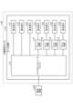
- FIG. 3 is a diagram showing an example of an arrangement of a plurality of light-emitting elements and a plurality of light-receiving elements provided on a sensor substrate.
- FIG. 4 is a diagram showing an example of a volume pulse wave detected by the photoelectric pulse wave sensor.
- FIG. 5 is a schematic diagram showing the positional relationship of multiple light-emitting elements and multiple light-receiving elements with respect to the arm of a wearer wearing a smart watch.
- FIG. 6 is a diagram showing an example of the relationship between the amount of displacement of the photoelectric pulse wave sensor in the circumferential direction of the arm and the amplitude of the pulse wave.
- FIG. 7 is a schematic diagram showing an example of the configuration of a photoplethysmographic sensor.
- FIG. 8 is a schematic diagram showing an example of the configuration of a microcomputer unit.
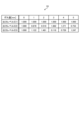
- FIG. 9 is a schematic diagram for explaining an example of the contents of the first correspondence information.
- FIG. 10 is a diagram showing an example of the content of the second correspondence information.
- FIG. 11 is a flowchart showing an example of the operation of a smart watch.
- the smart watch 1000 comprises a flat housing 1001, a display device 1002 attached to the surface of the housing, and a belt 1003 attached to two opposing sides of the housing 1001.
- the housing 1001 is made up of a top surface, a bottom surface, and sides connecting the periphery of the top surface and the periphery of the bottom surface.
- the housing is made up of a roughly rectangular parallelepiped and has four sides.
- FIG. 3 shows the arrangement of multiple light-emitting elements E and multiple light-receiving elements R provided on the sensor substrate 110.
- the sensor substrate 110 is rectangular.
- photodiodes or photosensors are used as an example of the multiple light receiving elements R.
- the light receiving elements R1 and R2 are arranged in parallel to the first row of the three light emitting elements E1, E2, and E3 at a position spaced apart from the first row in the +X direction.
- the light receiving elements R3 and R4 are arranged in parallel to the first row at a position spaced apart from the first row in the -X direction.
- the light emitting elements E1 to E3 emit light selected from a wavelength band that is easily absorbed by hemoglobin in blood, for example, a wavelength band from green to near infrared.
- the light emitting elements E1 to E3 emit light of the same wavelength and are each a light emitting diode (LED).
- the light receiving elements R1 to R4 can detect the light emitted by the light emitting elements E1 to E3.
- each of the light receiving elements R1 to R4 is a photodiode.
- the light-emitting elements E1 to E3 emit light toward the skin of the arm 400.
- the light-receiving elements R1 to R4 receive light that enters them, including light that penetrates under the skin and is reflected or scattered by the subcutaneous tissue and returns, and output a signal according to the amount of this light. This light that returns from the living body and enters the light-receiving elements R1 to R4 is sometimes called returned light.
- blood vessels including the radial artery, are present under the skin of the arm 400, the amount of returned light to the light-receiving elements R1 to R4 increases or decreases due to the influence of the blood vessel volume pulse waves.
- the photoelectric pulse wave sensor 100 provided in the smart watch 1000 detects the time change in the amount of light received by the light-receiving elements R1 to R4 as a volume pulse wave.
- FIG. 4 is a diagram showing an example of a volume pulse wave detected by the photoelectric pulse wave sensor 100.
- the horizontal axis indicates time
- the vertical axis indicates the waveform level (light intensity).
- the photoplethysmography sensor 100 can obtain a volume pulse wave waveform that periodically increases and decreases as shown in FIG. 4.
- this volume pulse wave waveform will be referred to simply as the pulse wave.
- the embodiment even if the position of the photoelectric pulse wave sensor 100 shifts due to body movement or the like, highly accurate pulse wave detection is possible. As a result, even if the wearer wears the belt 1003 loosely, the accuracy of pulse wave detection can be maintained.
- a plurality of light receiving elements R are arranged in a row on both sides of a first row of a plurality of light emitting elements E in parallel with each other and at equal intervals with respect to the first row. This makes it possible to prevent deterioration of detection accuracy due to misalignment of the direction in which the light-emitting elements E (and the light-receiving elements R) are arranged.
- the light emitting element E2 is located in the center of the sensor substrate 110.
- the front light emitting element is E1, and the front light emitting element is E3.
- the second row of light receiving elements R1 and R2 and the third row of light receiving elements R3 and R4 are disposed above and below the first row at equal intervals.
- the first imaginary line connecting light receiving elements R1 and R3 passes between light emitting elements E1 and E2.
- the second imaginary line on the left side connecting light receiving elements R2 and R4 passes between light emitting elements E2 and E3. Therefore, light emitting elements E1 and E3 are positioned to the right and left of the first and second imaginary lines by the same distance.
- a light emitting element E2 is provided at the center of the virtual rectangle.
- the radial artery 401 when projected in the Z-axis direction, overlaps with the light-emitting element E2 located in the center and is sandwiched between the light-emitting elements E1 and E3. In addition, in the Y-axis direction, the radial artery 401 is sandwiched between the light-receiving elements R1 and R2, and between the light-receiving elements R3 and R4.
- the light-emitting elements E1-E3 and the light-receiving elements R1-R4 are in such relative positions with respect to the radial artery 401, the light-emitting elements E1-E3 emit light, and the light that then returns from near the radial artery 401 can be efficiently received by the light-receiving elements R1-R4.
- the position of the photoplethysmographic sensor 100 that gives the positional relationship shown in Figure 5 is referred to as the normal position.
- the photoplethysmographic sensor 100 may shift: in the direction in which the arm 400 extends (i.e., the X-axis direction), and in the circumferential direction of the arm 400 (i.e., the Y-axis direction).
- this figure shows data obtained by performing an optical simulation assuming that the pitch of light-emitting elements E1, E2, and E3 is 5 mm, the distance between light-receiving elements R1 and R2 is 6 mm, and the distance between light-receiving elements R3 and R4 is 6 mm.
- the microcomputer unit 10 supplies power to the light-emitting elements E1 to E3, thereby causing the light-emitting elements E1 to E3 to emit light.
- the microcomputer unit 10 can adjust the output levels of the light-emitting elements E1 to E3 independently.
- the signal corresponding to the light received by the light receiving element R1 is amplified by the gain circuit 21 and input to the microcomputer unit 10.
- the signal corresponding to the light received by the light receiving element R3 is amplified by the gain circuit 23 and input to the microcomputer unit 10.
- the microcomputer unit 10 causes the light-emitting elements E1 to E3 to emit light, receives signals from the light-receiving elements R1 to R4 via the gain circuits 21 to 24, and calculates the pulse wave based on the received signals. The microcomputer unit 10 then outputs the calculated pulse wave to the display device 1002.
- FIG. 8 is a schematic diagram showing an example of the configuration of the microcomputer unit 10.
- RAM 12 is a volatile memory capable of high speed operation that is used as an area into which computer programs are loaded, a data buffer, or a data cache.
- processor 11 loads detection program 31 from ROM 14 into RAM 12 and executes detection program 31 in RAM 12.
- Output difference due to deviation Df (I(R2) + I(R4)) - (I(R1) + I(R3)) 5
- the light receiving elements R2 and R4 are arranged in a first region on the right side of the radial artery on the paper surface
- the light receiving elements R1 and R3 are arranged equally spaced apart in a second region on the left side of the radial artery on the paper surface.
- FIG. 10 is a diagram showing an example of the content of the second correspondence information 33. As shown in FIG. This second correspondence information 33 has a table structure, but the data structure of the second correspondence information 33 may be formed by a mathematical formula.
- the output level of the light-emitting element E1 is not changed, the output level of the light-emitting element E2 is raised, and the output level of the light-emitting element E3 is lowered, thereby eliminating the fluctuation in the amplitude of the pulse wave.
- Fluctuations in the amplitude of the pulse wave may be cancelled by changing the output levels of all of the light-emitting elements E1 to E3. Fluctuations in the amplitude of the pulse wave may be cancelled by simply increasing the output level of at least one of the light-emitting elements E1 to E3, or by simply decreasing the output level of at least one of the light-emitting elements E1 to E3.
- FIG. 11 is a flowchart showing an example of the operation of the smart watch 1000.
- Step 101 The processor 11 receives an instruction to start measurement by operation of the wearer or the like (S101).
- Step 102 The processor 11 drives the light-emitting elements E1, E2, and E3 to emit light at a predetermined output level (S102).
- the predetermined output level is the same output level as the output levels of the light-emitting elements E1, E2, and E3 when the first correspondence information 32 was generated.
- the light emitting elements E1, E2, and E3 are all driven at an output level of "1"
- the specified output level can be changed arbitrarily as long as it is the same as the output level of the light emitting elements E1, E2, and E3 when the first correspondence information 32 was generated. For example, only the light emitting element E2 may be driven at an output level of "1", and the light emitting elements E1 and E3 may be turned off.
- Step 103 Following S102, the processor 11 calculates the bias (difference) in the light receiving levels between the light receiving elements R1 and R3 and the light receiving elements R2 and R4 (S103).
- the bias is obtained by subtracting the sum of the signal strengths of light receiving elements R1 and R3 from the sum of the signal strengths of light receiving elements R2 and R4.
- a second row connecting the arrangement points of the first light receiving element and the second light receiving element, and a third row connecting the arrangement points of the third light receiving element and the fourth light receiving element are arranged at equal intervals from the first row.
Landscapes
- Health & Medical Sciences (AREA)
- Life Sciences & Earth Sciences (AREA)
- Cardiology (AREA)
- Engineering & Computer Science (AREA)
- Heart & Thoracic Surgery (AREA)
- Veterinary Medicine (AREA)
- Biophysics (AREA)
- Pathology (AREA)
- Public Health (AREA)
- Biomedical Technology (AREA)
- Physics & Mathematics (AREA)
- Medical Informatics (AREA)
- Molecular Biology (AREA)
- Surgery (AREA)
- Animal Behavior & Ethology (AREA)
- General Health & Medical Sciences (AREA)
- Physiology (AREA)
- Vascular Medicine (AREA)
- Measuring Pulse, Heart Rate, Blood Pressure Or Blood Flow (AREA)
Priority Applications (2)
| Application Number | Priority Date | Filing Date | Title |
|---|---|---|---|
| JP2024567186A JPWO2024142432A1 (https=) | 2022-12-27 | 2023-06-09 | |
| US19/248,633 US20250318738A1 (en) | 2022-12-27 | 2025-06-25 | Pulse wave detecting device |
Applications Claiming Priority (2)
| Application Number | Priority Date | Filing Date | Title |
|---|---|---|---|
| JP2022-210595 | 2022-12-27 | ||
| JP2022210595 | 2022-12-27 |
Related Child Applications (1)
| Application Number | Title | Priority Date | Filing Date |
|---|---|---|---|
| US19/248,633 Continuation US20250318738A1 (en) | 2022-12-27 | 2025-06-25 | Pulse wave detecting device |
Publications (1)
| Publication Number | Publication Date |
|---|---|
| WO2024142432A1 true WO2024142432A1 (ja) | 2024-07-04 |
Family
ID=91717198
Family Applications (1)
| Application Number | Title | Priority Date | Filing Date |
|---|---|---|---|
| PCT/JP2023/021574 Ceased WO2024142432A1 (ja) | 2022-12-27 | 2023-06-09 | 脈波検出装置および装着型脈波検出装置 |
Country Status (3)
| Country | Link |
|---|---|
| US (1) | US20250318738A1 (https=) |
| JP (1) | JPWO2024142432A1 (https=) |
| WO (1) | WO2024142432A1 (https=) |
Citations (8)
| Publication number | Priority date | Publication date | Assignee | Title |
|---|---|---|---|---|
| JP2006102159A (ja) * | 2004-10-06 | 2006-04-20 | Nippon Telegr & Teleph Corp <Ntt> | 生体情報計測装置 |
| JP2006271896A (ja) * | 2005-03-30 | 2006-10-12 | Toshiba Corp | 脈波検出装置及びその方法 |
| JP2009160274A (ja) * | 2008-01-08 | 2009-07-23 | Sharp Corp | 生体情報測定装置、生体情報測定方法、生体情報測定プログラムおよび記録媒体 |
| JP2010220638A (ja) * | 2009-03-19 | 2010-10-07 | Kanazawa Univ | 血圧情報測定装置 |
| JP2012019926A (ja) * | 2010-07-14 | 2012-02-02 | Rohm Co Ltd | 脈波センサ |
| JP2018007907A (ja) * | 2016-07-14 | 2018-01-18 | セイコーエプソン株式会社 | 検出装置および測定装置 |
| JP2018029870A (ja) * | 2016-08-26 | 2018-03-01 | セイコーエプソン株式会社 | 検出装置および検出方法 |
| WO2018147192A1 (ja) * | 2017-02-13 | 2018-08-16 | 学校法人帝京大学 | 脈波検出装置および方法 |
-
2023
- 2023-06-09 WO PCT/JP2023/021574 patent/WO2024142432A1/ja not_active Ceased
- 2023-06-09 JP JP2024567186A patent/JPWO2024142432A1/ja active Pending
-
2025
- 2025-06-25 US US19/248,633 patent/US20250318738A1/en active Pending
Patent Citations (8)
| Publication number | Priority date | Publication date | Assignee | Title |
|---|---|---|---|---|
| JP2006102159A (ja) * | 2004-10-06 | 2006-04-20 | Nippon Telegr & Teleph Corp <Ntt> | 生体情報計測装置 |
| JP2006271896A (ja) * | 2005-03-30 | 2006-10-12 | Toshiba Corp | 脈波検出装置及びその方法 |
| JP2009160274A (ja) * | 2008-01-08 | 2009-07-23 | Sharp Corp | 生体情報測定装置、生体情報測定方法、生体情報測定プログラムおよび記録媒体 |
| JP2010220638A (ja) * | 2009-03-19 | 2010-10-07 | Kanazawa Univ | 血圧情報測定装置 |
| JP2012019926A (ja) * | 2010-07-14 | 2012-02-02 | Rohm Co Ltd | 脈波センサ |
| JP2018007907A (ja) * | 2016-07-14 | 2018-01-18 | セイコーエプソン株式会社 | 検出装置および測定装置 |
| JP2018029870A (ja) * | 2016-08-26 | 2018-03-01 | セイコーエプソン株式会社 | 検出装置および検出方法 |
| WO2018147192A1 (ja) * | 2017-02-13 | 2018-08-16 | 学校法人帝京大学 | 脈波検出装置および方法 |
Also Published As
| Publication number | Publication date |
|---|---|
| US20250318738A1 (en) | 2025-10-16 |
| JPWO2024142432A1 (https=) | 2024-07-04 |
Similar Documents
| Publication | Publication Date | Title |
|---|---|---|
| US8660626B2 (en) | System and method for mitigating interference in pulse oximetry | |
| JP4607709B2 (ja) | 検出装置 | |
| US9814399B2 (en) | Biological information detection apparatus | |
| US7372778B2 (en) | Pulsometer worn on wrist and associated control method | |
| US11744519B2 (en) | Biological information measurement device | |
| US10098555B2 (en) | Biological information measurement apparatus | |
| JP6431697B2 (ja) | 手首装着型パルスオキシメータ | |
| US9826912B2 (en) | Photoplethysmographic device for measuring a heart rhythm | |
| JPWO1999012469A1 (ja) | 反射型光検出装置および生体情報計測装置 | |
| KR20100091592A (ko) | 손목형 맥파 측정장치 | |
| WO2015177867A1 (ja) | パルスオキシメータ | |
| US20230277073A1 (en) | Method for Obtaining Heart Rate and Electronic Device | |
| US10939855B2 (en) | Photoelectric sensor module | |
| JP4419540B2 (ja) | 脈波検出装置 | |
| WO2024142432A1 (ja) | 脈波検出装置および装着型脈波検出装置 | |
| JP7257571B2 (ja) | パルスオキシメータ | |
| US20220167888A1 (en) | Device for monitoring oxygen saturation levels in clinical conditions | |
| US12336797B2 (en) | Wrist-worn electronic device with optical cardiac monitor | |
| CN115886806A (zh) | 一种血氧检测的方法和装置 | |
| US12281935B2 (en) | Detecting device and measuring device | |
| JP2017189415A (ja) | 生体情報測定装置 | |
| CN219048476U (zh) | 一种心率检测模组及心率检测设备 | |
| JP7393275B2 (ja) | 脈波センサ付きバンド及び当該バンドを有する時計 | |
| KR102136317B1 (ko) | 정렬 오차 보상 방법 | |
| US20250281117A1 (en) | Medical sensor, and sensor supporting member |
Legal Events
| Date | Code | Title | Description |
|---|---|---|---|
| 121 | Ep: the epo has been informed by wipo that ep was designated in this application |
Ref document number: 23911216 Country of ref document: EP Kind code of ref document: A1 |
|
| WWE | Wipo information: entry into national phase |
Ref document number: 2024567186 Country of ref document: JP |
|
| NENP | Non-entry into the national phase |
Ref country code: DE |
|
| 122 | Ep: pct application non-entry in european phase |
Ref document number: 23911216 Country of ref document: EP Kind code of ref document: A1 |