WO2024141883A1 - 半導体装置 - Google Patents
半導体装置 Download PDFInfo
- Publication number
- WO2024141883A1 WO2024141883A1 PCT/IB2023/063061 IB2023063061W WO2024141883A1 WO 2024141883 A1 WO2024141883 A1 WO 2024141883A1 IB 2023063061 W IB2023063061 W IB 2023063061W WO 2024141883 A1 WO2024141883 A1 WO 2024141883A1
- Authority
- WO
- WIPO (PCT)
- Prior art keywords
- layer
- insulating layer
- conductive layer
- conductive
- semiconductor
- Prior art date
- Legal status (The legal status is an assumption and is not a legal conclusion. Google has not performed a legal analysis and makes no representation as to the accuracy of the status listed.)
- Ceased
Links
Images


Classifications
-
- H—ELECTRICITY
- H10—SEMICONDUCTOR DEVICES; ELECTRIC SOLID-STATE DEVICES NOT OTHERWISE PROVIDED FOR
- H10D—INORGANIC ELECTRIC SEMICONDUCTOR DEVICES
- H10D30/00—Field-effect transistors [FET]
- H10D30/01—Manufacture or treatment
- H10D30/021—Manufacture or treatment of FETs having insulated gates [IGFET]
-
- H—ELECTRICITY
- H10—SEMICONDUCTOR DEVICES; ELECTRIC SOLID-STATE DEVICES NOT OTHERWISE PROVIDED FOR
- H10D—INORGANIC ELECTRIC SEMICONDUCTOR DEVICES
- H10D30/00—Field-effect transistors [FET]
- H10D30/60—Insulated-gate field-effect transistors [IGFET]
- H10D30/67—Thin-film transistors [TFT]
-
- H—ELECTRICITY
- H10—SEMICONDUCTOR DEVICES; ELECTRIC SOLID-STATE DEVICES NOT OTHERWISE PROVIDED FOR
- H10D—INORGANIC ELECTRIC SEMICONDUCTOR DEVICES
- H10D84/00—Integrated devices formed in or on semiconductor substrates that comprise only semiconducting layers, e.g. on Si wafers or on GaAs-on-Si wafers
- H10D84/01—Manufacture or treatment
- H10D84/0123—Integrating together multiple components covered by H10D12/00 or H10D30/00, e.g. integrating multiple IGBTs
- H10D84/0126—Integrating together multiple components covered by H10D12/00 or H10D30/00, e.g. integrating multiple IGBTs the components including insulated gates, e.g. IGFETs
-
- H—ELECTRICITY
- H10—SEMICONDUCTOR DEVICES; ELECTRIC SOLID-STATE DEVICES NOT OTHERWISE PROVIDED FOR
- H10D—INORGANIC ELECTRIC SEMICONDUCTOR DEVICES
- H10D84/00—Integrated devices formed in or on semiconductor substrates that comprise only semiconducting layers, e.g. on Si wafers or on GaAs-on-Si wafers
- H10D84/01—Manufacture or treatment
- H10D84/02—Manufacture or treatment characterised by using material-based technologies
- H10D84/03—Manufacture or treatment characterised by using material-based technologies using Group IV technology, e.g. silicon technology or silicon-carbide [SiC] technology
- H10D84/038—Manufacture or treatment characterised by using material-based technologies using Group IV technology, e.g. silicon technology or silicon-carbide [SiC] technology using silicon technology, e.g. SiGe
-
- H—ELECTRICITY
- H10—SEMICONDUCTOR DEVICES; ELECTRIC SOLID-STATE DEVICES NOT OTHERWISE PROVIDED FOR
- H10K—ORGANIC ELECTRIC SOLID-STATE DEVICES
- H10K50/00—Organic light-emitting devices
-
- H—ELECTRICITY
- H10—SEMICONDUCTOR DEVICES; ELECTRIC SOLID-STATE DEVICES NOT OTHERWISE PROVIDED FOR
- H10K—ORGANIC ELECTRIC SOLID-STATE DEVICES
- H10K59/00—Integrated devices, or assemblies of multiple devices, comprising at least one organic light-emitting element covered by group H10K50/00
- H10K59/10—OLED displays
- H10K59/12—Active-matrix OLED [AMOLED] displays
Definitions
- one embodiment of the present invention is not limited to the above technical field.
- Examples of technical fields of one embodiment of the present invention disclosed in this specification and the like include semiconductor devices, display devices, light-emitting devices, power storage devices, memory devices, electronic devices, lighting devices, input devices, input/output devices, driving methods thereof, and manufacturing methods thereof.
- a semiconductor device refers to any device that can function by utilizing semiconductor characteristics.
- High-definition display panels mainly use light-emitting elements such as organic electroluminescence (EL) elements or light-emitting diodes (LEDs).
- EL organic electroluminescence
- LEDs light-emitting diodes
- Patent Document 1 discloses a high-definition display device that uses an organic EL device (also called an organic EL element).
- An object of one embodiment of the present invention is to provide a transistor that can be miniaturized. Another object is to form a transistor with an extremely short channel length and a transistor with a long channel length over the same substrate. Another object is to provide a transistor that can pass a large current. Another object is to provide a transistor with an extremely short channel length. Another object is to provide a transistor with reduced parasitic capacitance. Another object is to provide a transistor that occupies a small area. Another object is to provide a display device that can be easily made high-definition. Another object is to provide a highly reliable transistor, semiconductor device, and display device.
- An object of one embodiment of the present invention is to provide a semiconductor device, a display device, a memory device, or an electronic device having a novel structure.
- An object of one embodiment of the present invention is to alleviate at least one of the problems of the prior art.
- One aspect of the present invention is a semiconductor device having a first transistor and a first insulating layer.
- the first transistor has a first conductive layer, a second conductive layer, a third conductive layer, a fourth conductive layer, a first semiconductor layer, a second insulating layer, and a third insulating layer.
- the third insulating layer is located on the fourth conductive layer.
- the first insulating layer is located on the third insulating layer and overlaps with the fourth conductive layer, and has a first opening that reaches the third insulating layer.
- the first conductive layer and the second conductive layer are each located on the first insulating layer.
- the first semiconductor layer has a portion parallel to the sidewall of the first opening, a portion in contact with the first conductive layer, and a portion in contact with the second conductive layer.
- the second insulating layer covers the semiconductor layer in the first opening, and is in contact with the third insulating layer at the bottom of the first opening.
- the third conductive layer covers the second insulating layer within the first opening, and has a portion that overlaps with the fourth conductive layer at the bottom of the first opening without passing through the first semiconductor layer.
- the second transistor has a fifth conductive layer, a sixth conductive layer, a seventh conductive layer, and a second semiconductor layer.
- the first insulating layer has a second opening that reaches the fifth conductive layer.
- the sixth conductive layer is located on the first insulating layer.
- the second semiconductor layer has a portion that contacts the sixth conductive layer, a portion that is parallel to the sidewall of the second opening, and a portion that contacts the fifth conductive layer at the bottom of the second opening.
- the second insulating layer covers the second semiconductor layer in the second opening, and the seventh conductive layer covers the second insulating layer in the second opening.
- the fourth conductive layer has a portion located outside the first semiconductor layer in a plan view.
- a fourth insulating layer and a fifth insulating layer each located within the first opening.
- the fourth insulating layer is provided between the first semiconductor layer and the first insulating layer, and contains a material through which hydrogen is less likely to diffuse than the first insulating layer.
- the fifth insulating layer is provided between the first semiconductor layer and the fourth insulating layer, and has the function of capturing or fixing hydrogen.
- the sixth insulating layer is provided between the first semiconductor layer and the fifth insulating layer, and contains an oxide.
- the first conductive layer and the second conductive layer preferably have a first conductive film and a second conductive film thereon. Furthermore, it is preferable that the second conductive film contains ruthenium.
- the first conductive film contains indium and tin.
- the contour shape of the first opening is any one of a circle, an ellipse, a rectangle with rounded corners, a regular polygon, a polygon other than a regular polygon, a concave polygon, a polygon with rounded corners, or a closed curve that combines straight lines and curves.
- a transistor that can be miniaturized can be provided.
- a transistor with an extremely short channel length and a transistor with a long channel length can be separately formed on the same substrate.
- a transistor that can pass a large current can be provided.
- a transistor with an extremely short channel length can be provided.
- a transistor with reduced parasitic capacitance can be provided.
- a transistor that occupies a small area can be provided.
- a display device that can be easily made high-definition can be provided.
- a highly reliable transistor, semiconductor device, and display device can be provided.
- the present invention it is possible to provide a semiconductor device, a display device, a memory device, or an electronic device having a novel configuration. According to one aspect of the present invention, it is possible to at least alleviate at least one of the problems of the prior art.
- 1A to 1F show examples of the configuration of a semiconductor device.
- 2A to 2D show examples of the configuration of a semiconductor device.
- 3A and 3B show examples of the configuration of a semiconductor device.
- 4A to 4E show examples of the configuration of a semiconductor device.
- 5A to 5D show examples of the configuration of a semiconductor device.
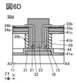
- 6A to 6D show examples of the configuration of a semiconductor device.
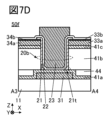
- 7A to 7D show examples of the configuration of a semiconductor device.
- 8A and 8B show examples of the configuration of a semiconductor device.
- 9A to 9D are diagrams illustrating an example of a method for manufacturing a semiconductor device.
- 10A to 10C are diagrams illustrating an example of a method for manufacturing a semiconductor device.
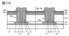
- 11A to 11C are diagrams illustrating an example of a method for manufacturing a semiconductor device.
- 12A to 12F show examples of the configuration of a semiconductor device.
- 13A and 13B show configuration examples of a semiconductor device.
- 14A and 14B show configuration examples of a semiconductor device.
- 15A to 15D are diagrams illustrating an example of a method for manufacturing a semiconductor device.
- 16A to 16C are diagrams illustrating an example of a method for manufacturing a semiconductor device.
- 17A and 17B are diagrams illustrating an example of a method for manufacturing a semiconductor device.
- 18A and 18B show configuration examples of the display device.
- FIG. 19 shows an example of the configuration of a display device.
- FIG. 20 shows an example of the configuration of a display device.
- FIG. 19 shows an example of the configuration of a display device.
- a display panel which is one aspect of a display device, has the function of displaying (outputting) images, etc. on a display surface. Therefore, a display panel is one aspect of an output device.
- a display panel having a connector such as an FPC (Flexible Printed Circuit) or TCP (Tape Carrier Package) attached to the substrate, or an IC mounted on the substrate using a COG (Chip On Glass) method or the like may be referred to as a display panel module, display module, or simply a display panel.
- FPC Flexible Printed Circuit
- TCP Transmission Carrier Package
- COG Chip On Glass
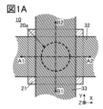
- One aspect of the present invention can be a configuration having two types of transistors fabricated separately on the same surface.
- One is a transistor in which a source electrode and a drain electrode are provided above and below an interlayer insulating layer so that they are located at different heights (for example, heights in a direction perpendicular to a substrate surface or insulating plane on which the transistor is provided), and a current flows in the height direction.
- the other is a transistor in which a current flows along the inner circumference of an opening provided in the interlayer insulating layer.
- the former can be a transistor with an extremely short channel length and capable of passing a large current because the channel length can be determined by the thickness of the interlayer insulating layer.
- the transistor of one embodiment of the present invention can also be called a VFET (Vertical Field Effect Transistor), a vertical transistor, a vertical channel transistor, etc.
- transistor 10 can have two or more of the source electrode, semiconductor, and drain electrode stacked, it can occupy a significantly smaller area than a so-called planar type transistor (which can also be called a lateral transistor, LFET (Lateral FET), etc.) in which the semiconductor is arranged on a plane.
- the conductive layer 32a may be made of indium-tin-silicon oxide (also called ITSO), which is a metal oxide, and the conductive layer 32b may be made of ruthenium.
- ITSO indium-tin-silicon oxide
- the conductive layer 32b may be made of ruthenium.
- the angle ⁇ of the sidewall of the opening 20a in the insulating layer 41 deviates from 90 degrees, the circumference of the opening 20a will differ depending on the height.
- the circumference at the height where the diameter of the opening 20a is smallest may be regarded as the channel width W, or the circumference at the height of the upper end of the opening 20a may be regarded as the channel width W.
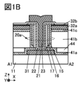
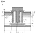
- insulating layer 15 has an L-shaped cross-sectional shape such that a part of it is located between the bottom surface of insulating layer 16 and the top surface of conductive layer 31.
- this shape can be achieved by continuously forming an insulating film that will become insulating layer 15 and an insulating film that will become insulating layer 16, and then removing parts of these by etching.
- transistor 50 will be described with reference to Figures 1D, 1E, and 1F. Note that descriptions of parts that overlap with those described above will be omitted.
- layers having the same function or layers formed in the same process in the transistors 10 and 50 will be described with the same reference numerals. Therefore, even if the layers in the transistors 10 and 50 are given the same reference numerals, they do not have to be the same (i.e., integral) layers.
- Transistor 50 has conductive layer 31, part of insulating layer 41a, semiconductor layer 21, insulating layer 22, conductive layer 23, conductive layer 33a, conductive layer 33b, conductive layer 34a, and conductive layer 34b.
- Conductive layer 33a and conductive layer 33b (hereinafter, sometimes collectively referred to as conductive layer 33) function as one of the source electrode and drain electrode, and conductive layer 34a and conductive layer 34b (hereinafter, sometimes collectively referred to as conductive layer 34) function as the other of the source electrode and drain electrode.
- a low-resistance region 21n is formed in the region of the semiconductor layer 21 that contacts the conductive layer 34b and in its vicinity, and a channel formation region 21i is formed in the portion that contacts the insulating layer 17.
- the channel width W of the transistor 50 is the length of the portion of the semiconductor layer 21 that contacts the insulating layer 17.
- the channel length L of the transistor 50 depends on the shape of the opening 20b and the thickness of each insulating layer located in the opening 20b. As shown in FIG. 3B, the semiconductor layer 21 has a ring-shaped shape that follows the opening 20b, so that two channels exist between the conductive layer 33a and the conductive layer 33b.
- the conductive layer 31 functions as a second gate electrode (or back gate electrode) of the transistor 50.
- the insulating layer 41a functions as a second gate insulating layer (back gate insulating layer).
- a fixed potential or any signal can be applied to the conductive layer 31.
- the potential on the back channel side (insulating layer 17 side) of the semiconductor layer 21 can be fixed, thereby reducing the variation in electrical characteristics.
- the conductive layer 31 may be electrically connected to any one of the conductive layers 33, 34, and 23, and the same potential may be applied to them.
- the electric field is applied to the semiconductor layer 21 from the diagonal rear by the conductive layer 31. Therefore, if the length (length G in FIG. 3A) of the portion of the conductive layer 31 that protrudes outward from the surface that becomes the back channel of the semiconductor layer 21 (here, the interface with the insulating layer 17) is too short, the function as a back gate may be reduced.
- the length G is preferably longer than half the thickness of the insulating layer 41b, and is preferably at least the thickness of the insulating layer 41b, preferably at least twice that length, and more preferably at least three times that length.
- the length G may be 20 times or less, preferably 10 times or less, the thickness of the insulating layer 41b.
- this is not limited to the direction in which the conductive layer 31 extends. This is also not limited to the case where the conductive layer 31 is shared by multiple transistors 50.
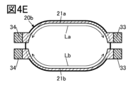
- Figures 4A to 4E show different examples of the semiconductor layer 21 and the opening 20b.
- Figures 4A to 4E are diagrams for explaining examples of the positional relationship between the opening 20b, the conductive layer 33, the conductive layer 34, and the semiconductor layer 21.
- FIG. 4A shows an example in which the contour of opening 20b has a shape that combines a circular arc and a straight line. This allows the distance between conductive layer 33 and conductive layer 34 to be extended, thereby lengthening the channel length L. Also, because there are two channels, the channel width W can be doubled.
- the semiconductor layer 21 is provided along the sidewall of the opening 20b.
- the channel length L of the transistor 50 corresponds to the distance between the conductive layer 33 and the conductive layer 34 along the outer periphery of the opening 20b.
- the channel width W of the transistor 50 is the width of the semiconductor layer 21 in the depth direction of the opening 20b. Therefore, since the channel width W can be controlled by the thickness of the insulating layer 41 and the depth of the opening 20b, a transistor with an extremely short channel width can be realized. For example, it is possible to realize a transistor with an extremely small channel width that could not be realized with a mass-production exposure tool. In addition, it is also possible to realize a transistor with a channel width of less than 10 nm without using the extremely expensive exposure tool used in cutting-edge LSI technology.
- metal oxides that can be used in the semiconductor layer 21 include In oxide, Ga oxide, and Zn oxide.
- the metal oxide preferably contains at least In or Zn.
- the metal oxide preferably contains two or three elements selected from In, element M, and Zn.
- the element M is a metal element or semimetal element with a high bond energy with oxygen, for example, a metal element or semimetal element with a bond energy with oxygen higher than that of indium.
- element M include Al, Ga, Sn, Y, Ti, V, Cr, Mn, Fe, Co, Ni, Zr, Mo, Hf, Ta, W, La, Ce, Nd, Mg, Ca, Sr, Ba, B, Si, Ge, and Sb.
- the metal oxide may contain one or more metal elements with a large periodic number.
- the field effect mobility of the transistor may be increased.
- metal elements with a large periodic number include metal elements belonging to the fifth period and metal elements belonging to the sixth period. Specific examples of such metal elements include Y, Zr, Ag, Cd, Sn, Sb, Ba, Pb, Bi, La, Ce, Pr, Nd, Pm, Sm, and Eu. La, Ce, Pr, Nd, Pm, Sm, and Eu are called light rare earth elements.
- the metal oxide can be formed preferably by sputtering or atomic layer deposition (ALD). In particular, it is preferable to form the metal oxide film by ALD, which has excellent coating properties.
- ALD atomic layer deposition
- the composition of the metal oxide film may differ from the composition of the target. In particular, the zinc content in the metal oxide film may decrease to about 50% compared to the target.
- an OS transistor When the transistor operates in the saturation region, an OS transistor can reduce the change in source-drain current in response to a change in gate-source voltage compared to a Si transistor. Therefore, by using an OS transistor as a driving transistor included in a pixel circuit, the amount of current flowing through the light-emitting device can be precisely controlled. This makes it possible to increase the gradation in the pixel circuit. Furthermore, even if the electrical characteristics (e.g., resistance) of the light-emitting device fluctuate or there is variation in the electrical characteristics, a stable current can flow.
- the electrical characteristics e.g., resistance
- OS transistors have small variations in electrical characteristics due to radiation exposure, i.e., they have high resistance to radiation, and therefore can be suitably used in environments where radiation may be present. It can also be said that OS transistors have high reliability against radiation.
- OS transistors can be suitably used in pixel circuits of X-ray flat panel detectors.
- OS transistors can also be suitably used in semiconductor devices used in outer space.
- radiation include electromagnetic radiation (e.g., X-rays and gamma rays) and particle radiation (e.g., alpha rays, beta rays, proton rays, and neutron rays).
- the semiconductor material that can be used for the semiconductor layer 21 is not limited to oxide semiconductors.
- a semiconductor made of a single element or a compound semiconductor can be used.
- semiconductors made of a single element include silicon (including single crystal silicon, polycrystalline silicon, microcrystalline silicon, and amorphous silicon) and germanium.
- compound semiconductors include gallium arsenide and silicon germanium.
- compound semiconductors include organic semiconductors, nitride semiconductors, and oxide semiconductors. These semiconductor materials may contain impurities as dopants.
- transition metal chalcogenides that can be used as the semiconductor layer of a transistor include molybdenum sulfide (representatively MoS 2 ), molybdenum selenide (representatively MoSe 2 ), molybdenum tellurium (representatively MoTe 2 ), tungsten sulfide (representatively WS 2 ), tungsten selenide (representatively WSe 2 ), tungsten tellurium (representatively WTe 2 ), hafnium sulfide (representatively HfS 2 ), hafnium selenide (representatively HfSe 2 ), zirconium sulfide (representatively ZrS 2 ), zirconium selenide (representatively ZrSe 2 ), and the like.
- the insulating layer 22 functions as a gate insulating layer of a transistor and can also be used as a dielectric layer of a capacitance element.
- an oxide semiconductor is used for the semiconductor layer 21, it is preferable to use an oxide insulating film for at least the film of the insulating layer 22 that is in contact with the semiconductor layer 21.
- silicon oxide, silicon oxynitride, aluminum oxide, aluminum oxynitride, hafnium oxide, hafnium oxynitride, gallium oxide, gallium oxynitride, yttrium oxide, yttrium oxynitride, and Ga-Zn oxide can be used.
- oxynitride refers to a material that contains more oxygen than nitrogen.
- Nitrogen oxide refers to a material that contains more nitrogen than oxygen.
- the insulating layer 22 is preferably made of a high-k insulating material, and preferably has a laminated structure of a high dielectric constant (high-k) material and a material with a higher dielectric strength than the high-k material.
- the insulating layer 22 can be made of an insulating film (also called ZAZ) in which zirconium oxide, aluminum oxide, and zirconium oxide are laminated in this order.
- an insulating film also called ZAZA in which zirconium oxide, aluminum oxide, zirconium oxide, and aluminum oxide are laminated in this order can be used.
- a material exhibiting ferroelectricity may be used as the insulating layer 22.
- materials exhibiting ferroelectricity include metal oxides such as hafnium oxide, zirconium oxide, and HfZrO x (x is a real number greater than 0).
- the conductive layer 31 and the conductive layer 32 are in contact with the semiconductor layer 21.
- an oxide semiconductor is used as the semiconductor layer 21
- a metal that is easily oxidized such as aluminum
- an insulating oxide e.g., aluminum oxide
- a conductive material that is not easily oxidized a conductive material that maintains low electrical resistance even when oxidized, or an oxide conductive material for at least the portion of the conductive layer 31 and the conductive layer 32 in contact with the semiconductor layer 21.
- the conductive layers 31 and 32 may be a single-layer structure of the conductive oxide film, a three-layer structure in which a titanium nitride film, a tungsten film, and a titanium nitride film are laminated in this order, a two-layer structure in which a ruthenium film or a ruthenium oxide film is laminated on tungsten, a two-layer structure in which a ruthenium film or a ruthenium oxide film is laminated on the conductive oxide film, or a two-layer structure in which the conductive oxide film is laminated on a ruthenium film or a ruthenium oxide film.
- ruthenium is a material that is difficult to etch, so when used, the thinner the better, and it is preferable to use a thickness of, for example, 0.1 nm to 2 nm.
- the insulating layer 17 has a portion in contact with the semiconductor layer 21.
- an oxide semiconductor is used for the semiconductor layer 21, it is preferable to use an oxide for at least the portion of the insulating layer 17 in contact with the semiconductor layer 21 in order to improve the interface characteristics between the semiconductor layer 21 and the insulating layer 17.
- silicon oxide or silicon oxynitride can be suitably used.
- the insulating layer 17 can be formed by a film formation method such as an ALD method, a sputtering method, or a plasma CVD method. In particular, it is preferable to form the insulating layer 17 by an ALD method.
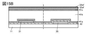
- the insulating layer 41b and the insulating layer 44 function as an interlayer insulating layer, it is preferable to use a film formation method that allows film formation at a high film formation rate compared to other insulating layers.
- the insulating layer 41b and the insulating layer 44 can be a TEOS (Tetra- Ethyl -Ortho-Silicate, chemical formula: Si( OC2H5 ) 4 ) film formed by plasma CVD. This can improve productivity.
- the insulating layer 41a, the insulating layer 41c, and the insulating layer 15 for example, one or more of silicon nitride, silicon nitride oxide, silicon oxynitride, aluminum oxide, aluminum oxynitride, aluminum nitride, hafnium oxide, and hafnium aluminate can be used.
- silicon nitride and silicon nitride oxide have the characteristics of releasing little impurities (e.g., water and hydrogen) from themselves and being difficult for oxygen and hydrogen to permeate, so they can be suitably used as the insulating layer 41a, the insulating layer 41c, and the insulating layer 15.
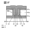
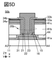
- ⁇ Variation 1> 5A and 5B show schematic cross-sectional views of transistor 10a and transistor 50a, respectively.
- the cross-sectional shape of insulating layer 15 is linear rather than L-shaped. Accordingly, the lower surface of insulating layer 16 is configured to contact insulating layer 41a. With this configuration, the contact area between insulating layer 17 and insulating layer 16 is increased, so that the hydrogen concentration in insulating layer 17 can be reduced more effectively.
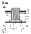
- a transistor 10b and a transistor 50b shown in FIGS. 5C and 5D differ from the transistor 10 and the transistor 50 described above mainly in that the insulating layer 17 is not provided.
- the insulating layer 16 is provided in contact with the semiconductor layer 21. Therefore, the insulating layer 16 can directly getter hydrogen in the semiconductor layer 21, and the hydrogen concentration in the semiconductor layer 21 can be effectively reduced. This makes it possible to realize a transistor with higher reliability. Furthermore, by not providing the insulating layer 17, the manufacturing process can be shortened, and productivity can be improved.
- the transistor 10c and the transistor 50c shown in FIGS. 6A and 6B differ from the transistor 10 and the transistor 50 described above mainly in that a conductive layer 26 is included.
- the conductive layer 26 is provided in a region surrounded by the insulating layers 41a, 41b, 41c, and 15. It can also be said that the conductive layer 26 is embedded in the insulating layer 41b. It is provided opposite the semiconductor layer 21 via the insulating layers 15, 16, and 17.
- conductive layer 26 functions as a third gate electrode. Insulating layers 15, 16, and 17 function as a third gate insulating layer. A fixed potential or any signal can be applied to conductive layer 26. It is preferable to apply the same potential as conductive layer 31 to conductive layer 26. Both conductive layer 26 and conductive layer 31 can apply an electric field to the back channel of semiconductor layer 21, so that the electrical characteristics can be stabilized more effectively.
- the insulating layer 41b has a sufficiently low hydrogen concentration.
- an oxide insulating film such as silicon oxide or silicon oxynitride formed by a sputtering method. This not only makes it possible to reduce the hydrogen concentration in the semiconductor layer 21 without using an insulating layer 16 having a function of gettering hydrogen and an insulating layer 15 having hydrogen barrier properties, but also makes it possible to supply a large amount of oxygen to the semiconductor layer 21, thereby realizing a highly reliable transistor.
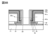
- FIG. 8A is a schematic cross-sectional view of a contact portion that can be formed on the same plane as transistors 10 and 50. Here, the contact portion between conductive layer 31 and conductive layer 32a is shown.
- FIG. 8B shows an example in which conductive layer 32b and conductive layer 32a disappear when insulating layer 15 and insulating layer 16 are formed. In this case, at least conductive layer 31 and conductive layer 32a remain in the portions overlapping with insulating layer 15 and insulating layer 16, so that the electrical connection between conductive layer 31 and conductive layer 32a is maintained.
- CVD methods can be classified into plasma CVD (PECVD) methods, which use plasma, thermal CVD (TCVD: Thermal CVD) methods, which use heat, and photo CVD (Photo CVD) methods, which use light. They can also be further divided into metal CVD (MCVD: Metal CVD) methods and metal organic CVD (MOCVD: Metal CVD) methods, depending on the source gas used.
- PECVD plasma CVD
- TCVD Thermal CVD
- Photo CVD Photo CVD
- MCVD Metal CVD
- MOCVD Metal CVD
- the ALD method can be a thermal ALD method in which the reaction between the precursor and reactant is carried out using only thermal energy, or a PEALD method in which a plasma-excited reactant is used.
- the insulating layer 11 can be an inorganic insulating film such as a silicon oxide film or a silicon oxynitride film.
- the insulating layer 11 can be formed by a sputtering method, a CVD method, an MBE method, a PLD method, an ALD method, or the like. If the surface on which the insulating layer 11 is to be formed is not flat, it is preferable to perform a planarization process so that the upper surface of the insulating layer 11 becomes flat after the insulating layer 11 is formed.
- a conductive film that will become the conductive layer 31 is formed on the insulating layer 11.
- a resist mask is formed on the conductive film by photolithography or the like, and the portion of the conductive film that is not covered by the resist mask is removed by etching, and then the resist mask is removed. This allows the conductive layer 31 to be formed.
- an insulating layer 41a is formed to cover the insulating layer 11 and the conductive layer 31.
- an insulating film that will become the insulating layer 44 is formed by forming an insulating film and removing the portion that overlaps with the conductive layer 31 (FIG. 9A).
- the insulating film that will become the insulating layer 44 is preferably processed by CMP (Chemical Mechanical Polishing), and for example, the insulating film is processed until the top surface of the insulating layer 41a is exposed, thereby forming the insulating layer 44 shown in FIG. 9A.
- CMP Chemical Mechanical Polishing
- the insulating layer 44 and the conductive layer 31 may be formed by first forming an insulating film that will become the insulating layer 44, then forming an opening in the insulating film, forming a conductive film to fill the opening, and performing a polishing process (planarization process) using the CMP method until the top surface of the insulating film is exposed.
- the insulating layer 41a may be formed to cover the insulating layer 44 and the conductive layer 31.
- insulating layer 41 By performing a planarization process so that the heights of the upper surfaces of insulating layer 44 and insulating layer 41a are the same, the upper surface of insulating layer 41, which is formed subsequently, can be made flat.
- insulating layer 41 may be provided to cover conductive layer 31 without providing insulating layer 44. In that case, it is preferable to perform a planarization process by CMP on the upper surface of insulating layer 41 to flatten the upper surface.
- the sidewalls of openings 20a and 20b are preferably as nearly perpendicular as possible to the top surface of conductive layer 31. With this configuration, a transistor with a small occupancy area can be fabricated.
- the sidewalls of openings 20a and 20b may be tapered. The tapered shape can improve the coverage of the film formed inside openings 20a and 20b.
- the maximum width of the openings 20a and 20b is preferably as fine as possible.
- the maximum width of the openings 20a and 20b is 2 ⁇ m or less, 1 ⁇ m or less, 500 nm or less, 300 nm or less, 150 nm or less, 100 nm or less, 60 nm or less, 50 nm or less, 40 nm or less, 30 nm or less, or 20 nm or less, and is preferably 5 nm or more.
- the gas used in the heat treatment is preferably highly purified.
- the amount of moisture contained in the gas used in the heat treatment is 1 ppb or less, preferably 0.1 ppb or less, and more preferably 0.05 ppb or less.
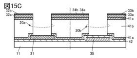
- insulating film 17f is anisotropically etched so that the upper surfaces of conductive layer 32b, conductive layer 33b, conductive layer 34b, and conductive layer 31 are exposed, thereby forming insulating layer 17 inside openings 20a and 20b ( Figure 10C).
- a resist mask 45 is formed to cover the opening 20b and its vicinity, and the insulating layer 41a located at the bottom of the opening 20a is removed by etching ( Figure 11A). After that, the resist mask is removed.
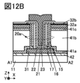
- the transistor 50A has a conductive layer 35 instead of the conductive layer 31. It also has an insulating layer 42 that covers the conductive layer 35.
- the conductive layer 35 functions as a second gate electrode, and the insulating layer 42 functions as a second gate insulating layer.
- conductive layer 35 is not in contact with semiconductor layer 21, and therefore various conductive materials can be used.
- conductive layer 35 any conductive material that can be used for conductive layer 23 can be appropriately selected.
- conductive layer 35 is used as wiring, it is preferable to use a conductive material with high conductivity.
- FIG. 14A is a schematic cross-sectional view including a contact portion between conductive layer 23 and conductive layer 32b. Note that the same configuration can be applied to conductive layers other than conductive layer 32b (conductive layer 33b, conductive layer 34b, or other conductive layers) formed in the same process as conductive layer 32b.
- Conductive layers 32a and 32b are stacked on insulating layer 41c, and insulating layer 22 is provided to cover them.
- Conductive layer 23 is provided on insulating layer 22.
- An opening is provided in insulating layer 22 that reaches conductive layer 32b, and conductive layer 23 and conductive layer 32b are in contact through this opening.
- FIG. 14B is a schematic cross-sectional view including the contact portion between conductive layer 35 and conductive layer 31. Note that the same configuration can be applied to conductive layers other than conductive layer 35 and conductive layer 31 that are formed in the same process.
- An insulating layer 42 is provided covering the conductive layer 35, and a conductive layer 31 is provided on the insulating layer 42.
- An opening is provided in the insulating layer 42 reaching the conductive layer 35, and the conductive layer 31 and the conductive layer 35 are in contact with each other through the opening.
- an insulating layer 11 is formed on a substrate (not shown).
- a conductive film that will become the conductive layer 35 is formed on the insulating layer 11, and unnecessary portions are removed by etching using a photolithography method to form the conductive layer 35.
- an insulating layer 42 is formed to cover the conductive layer 35.
- the insulating layer 42 can be formed by a method such as sputtering, CVD, MBE, PLD, or ALD, as appropriate.
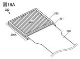
- Display module 18A shows a perspective view of a display module 280.
- the display module 280 includes a display device 200A and an FPC 290.
- the display panel included in the display module 280 is not limited to the display device 200A, and may be a display device 200B or a display device 200C described later.
- the display module 280 can be configured such that one or both of the pixel circuit section 283 and the circuit section 282 are provided overlappingly under the pixel section 284, so that the aperture ratio (effective display area ratio) of the display section 281 can be extremely high.
- the aperture ratio of the display section 281 can be 40% or more and less than 100%, preferably 50% or more and 95% or less, and more preferably 60% or more and 95% or less.
- the pixels 284a can be arranged at an extremely high density, so that the resolution of the display section 281 can be extremely high.
- display device 200A a separate light-emitting device is created for each emitted color, so there is little change in chromaticity between light emitted at low and high luminance.
- organic layers 112R, 112G, and 112B are spaced apart from each other, crosstalk between adjacent subpixels can be suppressed even in a high-definition display panel. This makes it possible to realize a display panel that is both high-definition and has high display quality.
- the pixel electrodes 111R, 111G, and 111B of the light-emitting element are electrically connected to the conductive layer 326 of the transistor 320 by the plug 256 embedded in the insulating layers 255a, 255b, and 255c, the conductive layer 241 embedded in the insulating layer 254, and the plug 274.
- the height of the top surface of the insulating layer 255c and the height of the top surface of the plug 256 are the same or approximately the same.
- Various conductive materials can be used for the plug.
- the semiconductor layer 351 is provided on the insulating layer 356.
- the semiconductor layer 351 preferably has a metal oxide (also called an oxide semiconductor) film that exhibits semiconductor characteristics.
- a pair of conductive layers 355 is provided on and in contact with the semiconductor layer 351 and functions as a source electrode and a drain electrode.
- an island-like light-emitting layer refers to a state in which the light-emitting layer is physically separated from the adjacent light-emitting layer.
- a part or the whole of the EL layer can be physically separated. This makes it possible to suppress leakage current between light-emitting elements via a layer shared between adjacent light-emitting elements (also called a common layer). This makes it possible to prevent crosstalk caused by unintended light emission, and to realize a display device with extremely high contrast. In particular, it makes it possible to realize a display device with high current efficiency at low luminance.
- FIG. 22A shows a schematic top view of a display device 100 according to one embodiment of the present invention.
- the display device 100 includes a plurality of light-emitting elements 110R that exhibit red light, a plurality of light-emitting elements 110G that exhibit green light, and a plurality of light-emitting elements 110B that exhibit blue light, over a substrate 101.
- the symbols R, G, and B are assigned within the light-emitting regions of the light-emitting elements in order to easily distinguish between the light-emitting elements.
- Light emitting elements 110R, 110G, and 110B are each arranged in a matrix.
- Figure 22A shows a so-called stripe arrangement in which light emitting elements of the same color are arranged in one direction. Note that the arrangement method of the light emitting elements is not limited to this, and arrangement methods such as an S-stripe arrangement, a delta arrangement, a Bayer arrangement, or a zigzag arrangement may also be applied, and a pentile arrangement, diamond arrangement, etc. may also be used.
- the light-emitting element 110R, the light-emitting element 110G, and the light-emitting element 110B for example, it is preferable to use an OLED (organic light-emitting diode) or a QLED (quantum-dot light-emitting diode).
- the light-emitting material possessed by the EL element include a material that emits fluorescence (fluorescent material), a material that emits phosphorescence (phosphorescent material), and a material that exhibits thermally activated delayed fluorescence (thermally activated delayed fluorescence (TADF) material).
- TADF thermally activated delayed fluorescence
- the light-emitting material possessed by the EL element not only organic compounds but also inorganic compounds (such as quantum dot materials) can be used.
- FIG. 22A also shows a connection electrode 111C that is electrically connected to the common electrode 113.
- the connection electrode 111C is given a potential (e.g., an anode potential or a cathode potential) to be supplied to the common electrode 113.
- the connection electrode 111C is provided outside the display area where the light-emitting elements 110R and the like are arranged.
- a protective layer 121 is provided on the common electrode 113, covering the light-emitting elements 110R, 110G, and 110B.
- the protective layer 121 has the function of preventing impurities such as water from diffusing from above into each light-emitting element.
- the end of the pixel electrode 111 is preferably tapered.
- the organic layer 112 provided along the end of the pixel electrode 111 can also be tapered.
- the coverage of the organic layer 112 provided over the end of the pixel electrode 111 can be improved.
- foreign matter for example, also called dust or particles
- a tapered shape refers to a shape in which at least a portion of the side of the structure is inclined with respect to the substrate surface.
- the structure it is preferable for the structure to have a region in which the angle between the inclined side and the substrate surface (also called the taper angle) is less than 90°.
- the organic layer 112 is processed into an island shape by photolithography. Therefore, the angle between the top surface and the side surface of the organic layer 112 at its edge is close to 90 degrees.
- an organic film formed using FMM (Fine Metal Mask) or the like tends to become gradually thinner the closer it is to the edge.
- the top surface is formed in a slope over a range of 1 ⁇ m to 10 ⁇ m to the edge, resulting in a shape in which it is difficult to distinguish between the top surface and the side surface.
- the resin layer 126 is located between the two adjacent light-emitting elements, and is provided so as to fill the ends of each organic layer 112 and the area between the two organic layers 112.
- the resin layer 126 has a smooth convex upper surface, and a common layer 114 and a common electrode 113 are provided covering the upper surface of the resin layer 126.
- the resin layer 126 functions as a planarization film that fills in the step between two adjacent light-emitting elements. By providing the resin layer 126, it is possible to prevent the phenomenon in which the common electrode 113 is divided by the step at the end of the organic layer 112 (also called step disconnection), which would cause the common electrode on the organic layer 112 to become insulated.
- the resin layer 126 can also be called an LFP (Local Filling Planarization) layer.
- an insulating layer containing an organic material can be suitably used.
- acrylic resin, polyimide resin, epoxy resin, imide resin, polyamide resin, polyimideamide resin, silicone resin, siloxane resin, benzocyclobutene resin, phenol resin, and precursors of these resins can be applied.
- organic materials such as polyvinyl alcohol (PVA), polyvinyl butyral, polyvinylpyrrolidone, polyethylene glycol, polyglycerin, pullulan, water-soluble cellulose, or alcohol-soluble polyamide resin can be used.
- the resin layer 126 may contain a material that absorbs visible light.
- the resin layer 126 itself may be made of a material that absorbs visible light, or the resin layer 126 may contain a pigment that absorbs visible light.
- the resin layer 126 may be, for example, a resin that can be used as a color filter that transmits red, blue, or green light and absorbs other light, or a resin that contains carbon black as a pigment and functions as a black matrix.
- the insulating layer 125 is located between the resin layer 126 and the organic layer 112, and functions as a protective film to prevent the resin layer 126 from coming into contact with the organic layer 112. If the organic layer 112 and the resin layer 126 come into contact with each other, the organic layer 112 may dissolve due to the organic solvent used in forming the resin layer 126. Therefore, by providing the insulating layer 125 between the organic layer 112 and the resin layer 126, it is possible to protect the side surface of the organic layer 112.
- the insulating layer 125 may be an insulating layer containing an inorganic material.
- an inorganic insulating film such as an oxide insulating film, a nitride insulating film, an oxynitride insulating film, and a nitride oxide insulating film may be used for the insulating layer 125.
- the insulating layer 125 may have a single layer structure or a laminated structure.
- the oxide insulating film examples include a silicon oxide film, an aluminum oxide film, a magnesium oxide film, an indium gallium zinc oxide film, a gallium oxide film, a germanium oxide film, an yttrium oxide film, a zirconium oxide film, a lanthanum oxide film, a neodymium oxide film, a hafnium oxide film, and a tantalum oxide film.
- the nitride insulating film include a silicon nitride film and an aluminum nitride film.
- the oxynitride insulating film examples include a silicon oxynitride film and an aluminum oxynitride film.
- nitride oxide insulating film examples include a silicon nitride oxide film and an aluminum nitride oxide film.
- an inorganic insulating film such as an aluminum oxide film or a hafnium oxide film formed by the ALD method to the insulating layer 125, an insulating layer 125 with few pinholes and excellent function of protecting the EL layer can be formed.
- oxynitride refers to a material whose composition contains more oxygen than nitrogen
- nitride oxide refers to a material whose composition contains more nitrogen than oxygen
- silicon oxynitride refers to a material whose composition contains more oxygen than nitrogen
- silicon nitride oxide refers to a material whose composition contains more nitrogen than oxygen
- the insulating layer 125 can be formed by sputtering, CVD, PLD, ALD, or the like. It is preferable to form the insulating layer 125 by the ALD method, which has good coating properties.
- a reflective film e.g., a metal film containing one or more selected from silver, palladium, copper, titanium, aluminum, etc.
- a reflective film may be provided between the insulating layer 125 and the resin layer 126, and the light emitted from the light-emitting layer may be reflected by the reflective film. This can improve the light extraction efficiency.
- Layer 128 is a portion of a protective layer (also called a mask layer or a sacrificial layer) that protects organic layer 112 when the organic layer 112 is etched.
- a protective layer also called a mask layer or a sacrificial layer
- the material that can be used for insulating layer 125 can be used for layer 128. In particular, it is preferable to use the same material for layer 128 and insulating layer 125, since the same processing equipment can be used for both layers.
- inorganic insulating films such as aluminum oxide films, metal oxide films such as hafnium oxide films, and silicon oxide films formed by the ALD method have few pinholes, so they have excellent functionality for protecting the EL layer and can be suitably used for insulating layer 125 and layer 128.
- the protective layer 121 can have, for example, a single-layer structure or a laminated structure including at least an inorganic insulating film.
- the inorganic insulating film include oxide films or nitride films such as a silicon oxide film, a silicon oxynitride film, a silicon nitride oxide film, a silicon nitride film, an aluminum oxide film, an aluminum oxynitride film, and a hafnium oxide film.
- a semiconductor material or a conductive material such as indium gallium oxide, indium zinc oxide, indium tin oxide, or indium gallium zinc oxide may be used as the protective layer 121.
- the protective layer 121 may be a laminated film of an inorganic insulating film and an organic insulating film.
- an organic insulating film is sandwiched between a pair of inorganic insulating films.
- the organic insulating film it is preferable for the organic insulating film to function as a planarizing film. This allows the upper surface of the organic insulating film to be flat, improving the coverage of the inorganic insulating film thereon and enhancing the barrier properties.
- the upper surface of the protective layer 121 is flat, it is preferable that when a structure (e.g., a color filter, an electrode of a touch sensor, or a lens array) is provided above the protective layer 121, the effect of uneven shapes caused by the structure below can be reduced.
- a structure e.g., a color filter, an electrode of a touch sensor, or a lens array
- FIG. 22C shows a connection portion 140 where the connection electrode 111C and the common electrode 113 are electrically connected.
- connection portion 140 an opening is provided in the insulating layer 125 and the resin layer 126 above the connection electrode 111C.
- the connection electrode 111C and the common electrode 113 are electrically connected in the opening.
- FIG. 22C shows a connection portion 140 that electrically connects the connection electrode 111C and the common electrode 113
- the common electrode 113 may be provided on the connection electrode 111C via the common layer 114.
- the electrical resistivity of the material used for the common layer 114 is sufficiently low and the layer can be formed thin, so that there are many cases where no problem occurs even if the common layer 114 is located at the connection portion 140. This allows the common electrode 113 and the common layer 114 to be formed using the same shielding mask, thereby reducing manufacturing costs.
- FIG. 23A shows a schematic cross-sectional view of the display device 100a.
- the display device 100a differs from the display device 100 described above mainly in that the light-emitting element has a different configuration and in that the display device 100a has a colored layer.
- the display device 100a has a light-emitting element 110W that emits white light.
- the light-emitting element 110W has a pixel electrode 111, an organic layer 112W, a common layer 114, and a common electrode 113.
- the organic layer 112W emits white light.
- the organic layer 112W can be configured to include two or more types of light-emitting materials whose emitted light colors are complementary to each other.
- the organic layer 112W can be configured to include a light-emitting organic compound that emits red light, a light-emitting organic compound that emits green light, and a light-emitting organic compound that emits blue light. It may also be configured to include a light-emitting organic compound that emits blue light and a light-emitting organic compound that emits yellow light.
- the organic layers 112W are separated between two adjacent light-emitting elements 110W. This makes it possible to suppress leakage current flowing between adjacent light-emitting elements 110W via the organic layers 112W, and to suppress crosstalk caused by the leakage current. This makes it possible to realize a display device with high contrast and color reproducibility.
- An insulating layer 122 that functions as a planarizing film is provided on the protective layer 121, and colored layers 116R, 116G, and 116B are provided on the insulating layer 122.
- the insulating layer 122 can be an organic resin film or an inorganic insulating film with a flattened upper surface.
- the insulating layer 122 forms the surface on which the colored layers 116R, 116G, and 116B are formed. Therefore, by making the upper surface of the insulating layer 122 flat, the thickness of the colored layers 116R, etc. can be made uniform, thereby improving the color purity. Note that if the thickness of the colored layers 116R, etc. is not uniform, the amount of light absorbed will vary depending on the location of the colored layer 116R, which may result in a decrease in color purity.
- Light-emitting element 110R has pixel electrode 111, conductive layer 115R, organic layer 112W, and common electrode 113.
- Light-emitting element 110G has pixel electrode 111, conductive layer 115G, organic layer 112W, and common electrode 113.
- Light-emitting element 110B has pixel electrode 111, conductive layer 115B, organic layer 112W, and common electrode 113.
- Conductive layer 115R, conductive layer 115G, and conductive layer 115B each have translucency and function as an optical adjustment layer.
- a microresonator (microcavity) structure By using a film that reflects visible light for the pixel electrode 111 and a film that is both reflective and transparent to visible light for the common electrode 113, a microresonator (microcavity) structure can be realized.
- a microresonator (microcavity) structure By adjusting the thicknesses of the conductive layers 115R, 115G, and 115B so as to provide optimal optical path lengths, it is possible to obtain intensified light of different wavelengths from the light-emitting elements 110R, 110G, and 110B, even when an organic layer 112 that emits white light is used.
- colored layers 116R, 116G, and 116B are provided on the optical paths of light-emitting elements 110R, 110G, and 110B, respectively, to obtain light with high color purity.
- an insulating layer 123 is provided to cover the ends of the pixel electrode 111 and the conductive layer 115.
- the insulating layer 123 preferably has a tapered end.
- the organic layer 112W and the common electrode 113 are each provided as a continuous film common to each light-emitting element. This configuration is preferable because it can greatly simplify the manufacturing process of the display device.
- This embodiment can be implemented by combining at least a portion of it with other embodiments described in this specification.
- the electronic device of this embodiment has a display panel (display device) in which a transistor of one embodiment of the present invention is applied to a display portion.
- the display device of one embodiment of the present invention can easily achieve high definition and high resolution, and can also achieve high display quality. Therefore, the display device can be used in the display portion of various electronic devices.
- Electronic devices include, for example, electronic devices with relatively large screens such as television sets, desktop or notebook personal computers, computer monitors, digital signage, large game machines such as pachinko machines, as well as digital cameras, digital video cameras, digital photo frames, mobile phones, portable game machines, personal digital assistants, and audio playback devices.
- the display panel of one embodiment of the present invention is capable of increasing the resolution, and therefore can be suitably used in electronic devices having a relatively small display.
- electronic devices include wristwatch-type and bracelet-type information terminals (wearable devices), as well as wearable devices that can be worn on the head, such as VR devices such as head-mounted displays, glasses-type AR devices, and MR devices.
- the display panel of one embodiment of the present invention preferably has an extremely high resolution such as HD (1280 x 720 pixels), FHD (1920 x 1080 pixels), WQHD (2560 x 1440 pixels), WQXGA (2560 x 1600 pixels), 4K (3840 x 2160 pixels), or 8K (7680 x 4320 pixels).
- an extremely high resolution such as HD (1280 x 720 pixels), FHD (1920 x 1080 pixels), WQHD (2560 x 1440 pixels), WQXGA (2560 x 1600 pixels), 4K (3840 x 2160 pixels), or 8K (7680 x 4320 pixels).
- HD 1280 x 720 pixels
- FHD (1920 x 1080 pixels
- WQHD 2560 x 1440 pixels
- WQXGA 2560 x 1600 pixels
- 4K 3840 x 2160 pixels
- 8K 8K
- the pixel density (resolution) of the display panel of one embodiment of the present invention is preferably 100 ppi or more, more preferably 300 ppi or more, more preferably 500 ppi or more, more preferably 1000 ppi or more, more preferably 2000 ppi or more, more preferably 3000 ppi or more, more preferably 5000 ppi or more, and even more preferably 7000 ppi or more.
- the screen ratio (aspect ratio) of the display panel of one embodiment of the present invention can support various screen ratios such as 1:1 (square), 4:3, 16:9, and 16:10.
- the electronic device of this embodiment may have a sensor (including a function to sense, detect, or measure force, displacement, position, velocity, acceleration, angular velocity, rotation speed, distance, light, liquid, magnetism, temperature, chemical substances, sound, time, hardness, electric field, current, voltage, power, radiation, flow rate, humidity, gradient, vibration, odor, or infrared light).
- a sensor including a function to sense, detect, or measure force, displacement, position, velocity, acceleration, angular velocity, rotation speed, distance, light, liquid, magnetism, temperature, chemical substances, sound, time, hardness, electric field, current, voltage, power, radiation, flow rate, humidity, gradient, vibration, odor, or infrared light).
- the electronic device of this embodiment can have various functions. For example, it can have a function to display various information (still images, videos, text images, etc.) on the display unit, a touch panel function, a function to display a calendar, date or time, etc., a function to execute various software (programs), a wireless communication function, a function to read out programs or data recorded on a recording medium, etc.
- a function to display various information still images, videos, text images, etc.
- a touch panel function a function to display a calendar, date or time, etc.
- a function to execute various software (programs) a wireless communication function
- a function to read out programs or data recorded on a recording medium etc.
- FIG. 24A to 24D An example of a wearable device that can be worn on the head will be described using Figures 24A to 24D.
- These wearable devices have one or both of the functions of displaying AR content and VR content. Note that these wearable devices may also have the function of displaying SR or MR content in addition to AR and VR.
- the electronic device may also have an earphone unit.
- Electronic device 700B shown in FIG. 24B has earphone unit 727.
- earphone unit 727 and the control unit may be configured to be connected to each other by wire.
- Part of the wiring connecting earphone unit 727 and the control unit may be disposed inside housing 721 or attachment unit 723.
- both glasses-type devices such as electronic device 700A and electronic device 700B
- goggle-type devices such as electronic device 800A and electronic device 800B
- FIG. 25D shows an example of a notebook personal computer.
- the notebook personal computer 7200 has a housing 7211, a keyboard 7212, a pointing device 7213, an external connection port 7214, a control device 7216, and the like.
- a display portion 7000 is incorporated in the housing 7211.
- the control device 7216 has, for example, one or more selected from a CPU, a GPU, and a storage device.
- the semiconductor device of one embodiment of the present invention can be applied to the display portion 7000, the control device 7216, and the like.
- the use of the semiconductor device of one embodiment of the present invention for the control device 7216 is preferable because power consumption can be reduced.
- a touch panel By applying a touch panel to the display unit 7000, not only can images or videos be displayed on the display unit 7000, but the user can also intuitively operate it, which is preferable. Furthermore, when used to provide information such as route information or traffic information, the intuitive operation can improve usability.
- the digital signage 7300 or the digital signage 7400 can be linked via wireless communication with an information terminal 7311 or an information terminal 7411 such as a smartphone carried by a user.
- advertising information displayed on the display unit 7000 can be displayed on the screen of the information terminal 7311 or the information terminal 7411.
- the display on the display unit 7000 can be switched by operating the information terminal 7311 or the information terminal 7411.
- the electronic device shown in Figures 26A to 26G has a housing 9000, a display unit 9001, a speaker 9003, operation keys 9005 (including a power switch or an operation switch), a connection terminal 9006, a sensor 9007 (including a function to sense, detect, or measure force, displacement, position, speed, acceleration, angular velocity, rotation speed, distance, light, liquid, magnetism, temperature, chemical substance, sound, time, hardness, electric field, current, voltage, power, radiation, flow rate, humidity, gradient, vibration, odor, or infrared light), a microphone 9008, etc.
- the structure of the transistor used in the device simulation is shown in FIG. 27.
- the transistor has a conductive layer 31 on an insulating layer 11, an insulating layer 42 on the conductive layer 31, insulating layers 41a, 41b, and 41c on the insulating layer 42, conductive layers 33 and 34 on the insulating layer 41c, insulating layers 15 and 16 located in openings provided in the insulating layers 41a, 41b, and 41c, a semiconductor layer 21 provided along the inner periphery of the opening, an insulating layer 22 covering the semiconductor layer 21, and a conductive layer 23 on the insulating layer 22.
- the insulating layer 42 is a layer that functions as a second gate insulating layer.
- the insulating layer 15 is not provided on the side surfaces of the conductive layers 33 and 34, and the semiconductor layer 21 is in contact with the side surfaces of the conductive layers 33 and 34.
- the insulating layer 22 has a four-layer structure (insulating layers 22-1 to 22-4), and the insulating layer 42 has a two-layer structure (insulating layers 42-1 and 42-2).
- Vsh shift voltage
- Id-Vg drain current-gate voltage characteristics
- the source voltage (Vs) was used as the reference
- the drain voltage (Vd) was set to 0.1 V
- the back gate voltage (Vbg) was set to three conditions: 0 V, -3 V, and -6 V.
- the gate voltage (Vg) was varied from -4 V to 4 V.
- FIG. 28A shows the backgate voltage dependence of the calculated shift voltage (Vsh). It was confirmed that the shift voltage changes linearly depending on the backgate voltage. Therefore, it was confirmed that the conductive layer 31 functions as a backgate even in a configuration in which the semiconductor layer 21 is disposed perpendicular to the conductive layer 31.
- the calculated Id-Vg characteristics are shown in Figure 28B.
- the calculated field effect mobility ( ⁇ FE) is also shown in Figure 28B. As shown in Figure 28B, it was confirmed that when the back gate voltage was changed, the characteristic curve shifted horizontally without any decrease in the current value or mobility.
Landscapes
- Engineering & Computer Science (AREA)
- Microelectronics & Electronic Packaging (AREA)
- Physics & Mathematics (AREA)
- Optics & Photonics (AREA)
- Thin Film Transistor (AREA)
Priority Applications (1)
| Application Number | Priority Date | Filing Date | Title |
|---|---|---|---|
| JP2024566914A JPWO2024141883A1 (https=) | 2022-12-28 | 2023-12-21 |
Applications Claiming Priority (4)
| Application Number | Priority Date | Filing Date | Title |
|---|---|---|---|
| JP2022211410 | 2022-12-28 | ||
| JP2022-211413 | 2022-12-28 | ||
| JP2022-211410 | 2022-12-28 | ||
| JP2022211413 | 2022-12-28 |
Publications (1)
| Publication Number | Publication Date |
|---|---|
| WO2024141883A1 true WO2024141883A1 (ja) | 2024-07-04 |
Family
ID=91716595
Family Applications (1)
| Application Number | Title | Priority Date | Filing Date |
|---|---|---|---|
| PCT/IB2023/063061 Ceased WO2024141883A1 (ja) | 2022-12-28 | 2023-12-21 | 半導体装置 |
Country Status (2)
| Country | Link |
|---|---|
| JP (1) | JPWO2024141883A1 (https=) |
| WO (1) | WO2024141883A1 (https=) |
Cited By (1)
| Publication number | Priority date | Publication date | Assignee | Title |
|---|---|---|---|---|
| WO2026058122A1 (ja) * | 2024-09-13 | 2026-03-19 | 株式会社半導体エネルギー研究所 | 半導体装置 |
Citations (5)
| Publication number | Priority date | Publication date | Assignee | Title |
|---|---|---|---|---|
| JP2012195574A (ja) * | 2011-03-03 | 2012-10-11 | Semiconductor Energy Lab Co Ltd | 半導体記憶装置およびその作製方法 |
| JP2012199536A (ja) * | 2011-03-10 | 2012-10-18 | Semiconductor Energy Lab Co Ltd | 半導体記憶装置 |
| JP2015005735A (ja) * | 2013-05-20 | 2015-01-08 | 株式会社半導体エネルギー研究所 | 半導体装置 |
| JP2016149552A (ja) * | 2015-02-11 | 2016-08-18 | 株式会社半導体エネルギー研究所 | 半導体装置、および半導体装置の作製方法 |
| US20220149166A1 (en) * | 2020-11-11 | 2022-05-12 | Samsung Electronics Co., Ltd. | Field-effect transistor, field-effect transistor array structure and method of manufacturing field-effect transistor |
-
2023
- 2023-12-21 WO PCT/IB2023/063061 patent/WO2024141883A1/ja not_active Ceased
- 2023-12-21 JP JP2024566914A patent/JPWO2024141883A1/ja active Pending
Patent Citations (5)
| Publication number | Priority date | Publication date | Assignee | Title |
|---|---|---|---|---|
| JP2012195574A (ja) * | 2011-03-03 | 2012-10-11 | Semiconductor Energy Lab Co Ltd | 半導体記憶装置およびその作製方法 |
| JP2012199536A (ja) * | 2011-03-10 | 2012-10-18 | Semiconductor Energy Lab Co Ltd | 半導体記憶装置 |
| JP2015005735A (ja) * | 2013-05-20 | 2015-01-08 | 株式会社半導体エネルギー研究所 | 半導体装置 |
| JP2016149552A (ja) * | 2015-02-11 | 2016-08-18 | 株式会社半導体エネルギー研究所 | 半導体装置、および半導体装置の作製方法 |
| US20220149166A1 (en) * | 2020-11-11 | 2022-05-12 | Samsung Electronics Co., Ltd. | Field-effect transistor, field-effect transistor array structure and method of manufacturing field-effect transistor |
Cited By (1)
| Publication number | Priority date | Publication date | Assignee | Title |
|---|---|---|---|---|
| WO2026058122A1 (ja) * | 2024-09-13 | 2026-03-19 | 株式会社半導体エネルギー研究所 | 半導体装置 |
Also Published As
| Publication number | Publication date |
|---|---|
| JPWO2024141883A1 (https=) | 2024-07-04 |
Similar Documents
| Publication | Publication Date | Title |
|---|---|---|
| KR20240016906A (ko) | 반도체 장치 및 반도체 장치의 제작 방법 | |
| WO2023203425A1 (ja) | 半導体装置及び半導体装置の作製方法 | |
| WO2023218280A1 (ja) | 半導体装置、及び、半導体装置の作製方法 | |
| WO2023209493A1 (ja) | 半導体装置及び半導体装置の作製方法 | |
| JP2025146915A (ja) | 半導体装置 | |
| WO2024141887A1 (ja) | 半導体装置 | |
| WO2024157122A1 (ja) | 半導体装置 | |
| WO2024141883A1 (ja) | 半導体装置 | |
| WO2024201262A1 (ja) | 半導体装置及び半導体装置の作製方法 | |
| US20250220972A1 (en) | Semiconductor device | |
| WO2024141879A1 (ja) | 半導体装置 | |
| WO2024209327A1 (ja) | 半導体装置、及び表示装置 | |
| JP2024158715A (ja) | 半導体装置、及び、半導体装置の作製方法 | |
| US20240421208A1 (en) | Semiconductor device and method for manufacturing the semiconductor device | |
| WO2025078929A1 (ja) | 半導体装置、及びその作製方法 | |
| WO2024141865A1 (ja) | 半導体装置、及び、半導体装置の作製方法 | |
| WO2024161260A1 (ja) | 半導体装置、及び、半導体装置の作製方法 | |
| WO2024121683A1 (ja) | 半導体装置 | |
| WO2024246718A1 (ja) | 半導体装置、及び、半導体装置の作製方法 | |
| WO2025233766A1 (ja) | 半導体装置、及び半導体装置の作製方法 | |
| WO2023227992A1 (ja) | 半導体装置 | |
| WO2024241137A1 (ja) | 半導体装置、及び、半導体装置の作製方法 | |
| WO2024013602A1 (ja) | トランジスタ、及び、トランジスタの作製方法 | |
| WO2024246661A1 (ja) | 半導体装置、及び表示装置 | |
| WO2024134442A1 (ja) | 半導体装置 |
Legal Events
| Date | Code | Title | Description |
|---|---|---|---|
| 121 | Ep: the epo has been informed by wipo that ep was designated in this application |
Ref document number: 23911081 Country of ref document: EP Kind code of ref document: A1 |
|
| WWE | Wipo information: entry into national phase |
Ref document number: 2024566914 Country of ref document: JP |
|
| NENP | Non-entry into the national phase |
Ref country code: DE |
|
| 122 | Ep: pct application non-entry in european phase |
Ref document number: 23911081 Country of ref document: EP Kind code of ref document: A1 |