WO2024101211A1 - セラミック電子部品の製造方法 - Google Patents
セラミック電子部品の製造方法 Download PDFInfo
- Publication number
- WO2024101211A1 WO2024101211A1 PCT/JP2023/039184 JP2023039184W WO2024101211A1 WO 2024101211 A1 WO2024101211 A1 WO 2024101211A1 JP 2023039184 W JP2023039184 W JP 2023039184W WO 2024101211 A1 WO2024101211 A1 WO 2024101211A1
- Authority
- WO
- WIPO (PCT)
- Prior art keywords
- electronic component
- ceramic
- support
- component body
- firing
- Prior art date
- Legal status (The legal status is an assumption and is not a legal conclusion. Google has not performed a legal analysis and makes no representation as to the accuracy of the status listed.)
- Ceased
Links
Images


Classifications
-
- B—PERFORMING OPERATIONS; TRANSPORTING
- B22—CASTING; POWDER METALLURGY
- B22F—WORKING METALLIC POWDER; MANUFACTURE OF ARTICLES FROM METALLIC POWDER; MAKING METALLIC POWDER; APPARATUS OR DEVICES SPECIALLY ADAPTED FOR METALLIC POWDER
- B22F3/00—Manufacture of workpieces or articles from metallic powder characterised by the manner of compacting or sintering; Apparatus specially adapted therefor ; Presses and furnaces
- B22F3/12—Both compacting and sintering
- B22F3/16—Both compacting and sintering in successive or repeated steps
-
- B—PERFORMING OPERATIONS; TRANSPORTING
- B28—WORKING CEMENT, CLAY, OR STONE
- B28B—SHAPING CLAY OR OTHER CERAMIC COMPOSITIONS; SHAPING SLAG; SHAPING MIXTURES CONTAINING CEMENTITIOUS MATERIAL, e.g. PLASTER
- B28B1/00—Producing shaped prefabricated articles from the material
- B28B1/30—Producing shaped prefabricated articles from the material by applying the material on to a core or other moulding surface to form a layer thereon
-
- B—PERFORMING OPERATIONS; TRANSPORTING
- B29—WORKING OF PLASTICS; WORKING OF SUBSTANCES IN A PLASTIC STATE IN GENERAL
- B29C—SHAPING OR JOINING OF PLASTICS; SHAPING OF MATERIAL IN A PLASTIC STATE, NOT OTHERWISE PROVIDED FOR; AFTER-TREATMENT OF THE SHAPED PRODUCTS, e.g. REPAIRING
- B29C64/00—Additive manufacturing, i.e. manufacturing of three-dimensional [3D] objects by additive deposition, additive agglomeration or additive layering, e.g. by 3D printing, stereolithography or selective laser sintering
- B29C64/10—Processes of additive manufacturing
- B29C64/106—Processes of additive manufacturing using only liquids or viscous materials, e.g. depositing a continuous bead of viscous material
- B29C64/112—Processes of additive manufacturing using only liquids or viscous materials, e.g. depositing a continuous bead of viscous material using individual droplets, e.g. from jetting heads
-
- B—PERFORMING OPERATIONS; TRANSPORTING
- B33—ADDITIVE MANUFACTURING TECHNOLOGY
- B33Y—ADDITIVE MANUFACTURING, i.e. MANUFACTURING OF THREE-DIMENSIONAL [3D] OBJECTS BY ADDITIVE DEPOSITION, ADDITIVE AGGLOMERATION OR ADDITIVE LAYERING, e.g. BY 3D PRINTING, STEREOLITHOGRAPHY OR SELECTIVE LASER SINTERING
- B33Y10/00—Processes of additive manufacturing
-
- H—ELECTRICITY
- H01—ELECTRIC ELEMENTS
- H01G—CAPACITORS; CAPACITORS, RECTIFIERS, DETECTORS, SWITCHING DEVICES, LIGHT-SENSITIVE OR TEMPERATURE-SENSITIVE DEVICES OF THE ELECTROLYTIC TYPE
- H01G4/00—Fixed capacitors; Processes of their manufacture
- H01G4/30—Stacked capacitors
-
- H—ELECTRICITY
- H01—ELECTRIC ELEMENTS
- H01C—RESISTORS
- H01C17/00—Apparatus or processes specially adapted for manufacturing resistors
-
- H—ELECTRICITY
- H01—ELECTRIC ELEMENTS
- H01F—MAGNETS; INDUCTANCES; TRANSFORMERS; SELECTION OF MATERIALS FOR THEIR MAGNETIC PROPERTIES
- H01F41/00—Apparatus or processes specially adapted for manufacturing or assembling magnets, inductances or transformers; Apparatus or processes specially adapted for manufacturing materials characterised by their magnetic properties
- H01F41/02—Apparatus or processes specially adapted for manufacturing or assembling magnets, inductances or transformers; Apparatus or processes specially adapted for manufacturing materials characterised by their magnetic properties for manufacturing cores, coils, or magnets
- H01F41/04—Apparatus or processes specially adapted for manufacturing or assembling magnets, inductances or transformers; Apparatus or processes specially adapted for manufacturing materials characterised by their magnetic properties for manufacturing cores, coils, or magnets for manufacturing coils
-
- H—ELECTRICITY
- H01—ELECTRIC ELEMENTS
- H01G—CAPACITORS; CAPACITORS, RECTIFIERS, DETECTORS, SWITCHING DEVICES, LIGHT-SENSITIVE OR TEMPERATURE-SENSITIVE DEVICES OF THE ELECTROLYTIC TYPE
- H01G13/00—Apparatus specially adapted for manufacturing capacitors; Processes specially adapted for manufacturing capacitors not provided for in groups H01G4/00 - H01G11/00
-
- H—ELECTRICITY
- H05—ELECTRIC TECHNIQUES NOT OTHERWISE PROVIDED FOR
- H05K—PRINTED CIRCUITS; CASINGS OR CONSTRUCTIONAL DETAILS OF ELECTRIC APPARATUS; MANUFACTURE OF ASSEMBLAGES OF ELECTRICAL COMPONENTS
- H05K3/00—Apparatus or processes for manufacturing printed circuits
Definitions
- the present invention relates to a method for manufacturing ceramic electronic components.
- Patent Document 1 discloses a method for manufacturing a multilayer electronic component, comprising the steps of: laminating a plurality of ceramic green sheets, in which at least an insulator, an internal electrode conductor, an external electrode conductor, and a dissipative material are patterned so that the portions that will become the corners of the multilayer electronic component after lamination are substantially spherically rounded; so that the dissipative material is patterned outside the substantially spherically rounded portions and continuous with the substantially spherically rounded portions at positions that correspond to the cuts for separating the ceramic green sheet stack into the multilayer electronic components; and performing a specific process on the ceramic green sheet stack to remove the regions made of the dissipative material and simultaneously separate the ceramic green sheet stack into individual multilayer electronic components.
- Patent Document 2 discloses a method for producing a ceramic object for electronic components, which is characterized by forming a three-dimensional shape by performing a dissipation process on a laminate made by stacking a plurality of sheet-like members having at least an insulating material and a dissipation material so that a ceramic object for electronic components can be obtained from the laminate.
- Patent Document 3 discloses a method for manufacturing a ceramic product, comprising: a process for forming a three-dimensional object having a ceramic body formed from the first ink and a glaze film formed from the second ink and covering at least a part of the ceramic body, by 3D printing in which a first ink containing a ceramic material and a second ink containing a glaze are sprayed and deposited by an inkjet method; and a firing process for firing the three-dimensional object formed by the process for forming the object.
- the present invention has been made to solve the above problems, and aims to provide a method for manufacturing ceramic electronic components that can suppress deformation during firing even when the components have complex shapes.
- the method for manufacturing a ceramic electronic component of the present invention is characterized by comprising the steps of: 3D printing a ceramic material, a metal material, and a vanishing material by a material jetting method to form a molded object having an electronic component body including the ceramic material and the metal material, a support including the ceramic material and provided on at least a portion of the periphery of the electronic component body, and a vanishing body including the vanishing material and provided between the electronic component body and the support; firing the molded object at a temperature equal to or higher than the temperature at which the vanishing body vanishes; and obtaining the electronic component body from which the support has been separated from the molded object after firing.
- the present invention provides a method for manufacturing ceramic electronic components that can suppress deformation during firing, even when the components have complex shapes.
- FIG. 1 is a schematic perspective view showing a shaped object formed in a shaped object forming step in a manufacturing method for a ceramic electronic component according to a first embodiment of the present invention.
- FIG. 2 is a schematic cross-sectional view showing an example of a cross section taken along line a1-a2 of the object shown in FIG.
- FIG. 3 is a schematic perspective view showing an electronic component body obtained in the step of obtaining an electronic component body in the manufacturing method for a ceramic electronic component according to the first embodiment of the present invention.
- FIG. 4 is a schematic perspective view showing a shaped object formed on a printing base in the step of forming a shaped object in the method for manufacturing a ceramic electronic component according to a modified example of the first preferred embodiment of the present invention.
- FIG. 1 is a schematic perspective view showing a shaped object formed in a shaped object forming step in a manufacturing method for a ceramic electronic component according to a first embodiment of the present invention.
- FIG. 2 is a schematic cross-sectional
- FIG. 5 is a schematic perspective view showing a shaped object formed in the step of forming a shaped object in the method for manufacturing a ceramic electronic component according to the second embodiment of the present invention.
- FIG. 6 is a schematic cross-sectional view showing an example of a cross section taken along the line segment b1-b2 of the object shown in FIG.
- FIG. 7 is a schematic perspective view showing an electronic component body with connectors obtained in the middle of the process of obtaining the electronic component body in the manufacturing method for a ceramic electronic component according to the second embodiment of the present invention.
- the manufacturing method of the ceramic electronic component of the present invention is described below. Note that the present invention is not limited to the configurations below, and may be modified as appropriate without departing from the gist of the present invention. In addition, a combination of multiple individual preferred configurations described below also constitutes the present invention.
- the method for manufacturing a ceramic electronic component of the present invention is characterized by comprising the steps of: 3D printing a ceramic material, a metal material, and a vanishing material by a material jetting method to form a molded object having an electronic component body including the ceramic material and the metal material, a support including the ceramic material and provided on at least a portion of the periphery of the electronic component body, and a vanishing body including the vanishing material and provided between the electronic component body and the support; firing the molded object at a temperature equal to or higher than the temperature at which the vanishing body vanishes; and obtaining the electronic component body from which the support has been separated from the molded object after firing.
- Fig. 1 is a schematic perspective view showing a shaped object formed in a step of forming a shaped object in a manufacturing method of a ceramic electronic component according to a first preferred embodiment of the present invention.
- Fig. 2 is a schematic cross-sectional view showing an example of a cross section taken along line segment a1-a2 of the shaped object shown in Fig. 1.
- the ceramic material, metal material, and dissipative material are 3D printed using the material jetting method to form the object 1A shown in Figures 1 and 2.
- the object 1A has an electronic component body 10, a support 20, and a vanishing body 30.
- the electronic component body 10 includes a ceramic material and a metal material.
- the electronic component body 10 has a ceramic part 11 that contains a ceramic material, and an electrode part 12 that contains a metal material and is in contact with the ceramic part 11.
- the electrode section 12 may be composed of one electrode member or multiple electrode members.
- the electrode portion 12 is composed of two electrode members: a first electrode member 13a that contacts one end of the ceramic portion 11, and a second electrode member 13b that contacts the other end of the ceramic portion 11.
- the position of the electrode portion 12 relative to the ceramic portion 11 is not particularly limited.
- the positions of the first electrode member 13a and the second electrode member 13b relative to the ceramic portion 11 are not limited to the positions shown in Figures 1 and 2.
- the support 20 includes a ceramic material.
- the ceramic material contained in the support 20 is preferably the same as the ceramic material contained in the electronic component body 10 (ceramic portion 11), but may be different from the ceramic material contained in the electronic component body 10 (ceramic portion 11).
- the support 20 is provided around at least a portion of the periphery of the electronic component body 10.
- the support 20 may be provided around a portion of the periphery of the electronic component body 10 as shown in FIG. 1, or it may be provided around the entire periphery of the electronic component body 10. In other words, the support 20 may cover a portion of the electronic component body 10 as shown in FIG. 1, or it may cover the entire electronic component body 10.
- the vanishing body 30 includes vanishing material.
- the vanishing body 30 is provided between the electronic component body 10 and the support 20. More specifically, the vanishing body 30 is provided so as to fill the gap between the electronic component body 10 and the support 20. In this way, the vanishing body 30 is in contact with both the electronic component body 10 and the support 20.
- Ceramic materials include, for example, alumina, aluminum nitride, low-temperature co-fired ceramic (LTCC) materials, etc. Among them, it is preferable that the ceramic material is a low-temperature co-fired ceramic material.
- low-temperature sintering ceramic materials refer to ceramic materials that can be sintered at firing temperatures of 1000°C or less.
- low-temperature sintering ceramic materials include glass composite low-temperature sintering ceramic materials including ceramic materials such as quartz, alumina, forsterite, and borosilicate glass, crystallized glass low-temperature sintering ceramic materials including ZnO-MgO-Al 2 O 3 -SiO 2 crystallized glass, non-glass low-temperature sintering ceramic materials including BaO-Al 2 O 3 -SiO 2 ceramic materials, Al 2 O 3 -CaO-SiO 2 -MgO-B 2 O 3 ceramic materials, etc.
- low-temperature sintering ceramic materials mainly made of alumina with added SiO 2 are preferable.
- the metal material is preferably a material that can be co-fired with the ceramic material, and more preferably a material that can be co-fired with the low-temperature sintering ceramic material.
- the melting point of the metal material is preferably higher than the sintering temperature of the ceramic material, and more preferably higher than the sintering temperature of the low-temperature sintering ceramic material.
- metal materials include copper, silver, and alloys containing at least one of these metals.
- the vanishing material is preferably a material that vanishes at or below the sintering temperature of the ceramic material, and more preferably a material that vanishes at or below the sintering temperature of the low-temperature sintering ceramic material.
- Examples of such vanishing materials include organic resins, carbon black, etc.
- the following method can be given as an example of a method for forming the object 1A using 3D printing with the material jetting method.
- a first ink containing a ceramic material, a second ink containing a metal material, and a third ink containing a vanishing material are prepared.
- each ink is sprayed from an inkjet head to coat the desired pattern, and the resulting coating is dried with hot air or the like.
- a ceramic layer containing a ceramic material, a metal layer containing a metal material, and a vanishing layer containing a vanishing material are laminated in the desired pattern.
- the object 1A is formed, which has an electronic component body 10 formed by laminating ceramic layers and metal layers, a support 20 formed by laminating ceramic layers, and a vanishing body 30 formed by laminating vanishing layers.
- the first ink may further contain a resin, a solvent, etc. in addition to the ceramic material.
- resins examples include ethyl cellulose, acrylic, and polyvinyl butyral. When such a resin is contained in the first ink, the resin solidifies when the coating film described above dries, and functions as a binder for the ceramic material. Such resins are removed, for example, when the shaped object is fired, as described below.
- the solvent examples include organic solvents such as methanol and ethanol, inorganic solvents such as water, and mixtures of these. Such solvents are removed, for example, when the coating film is dried as described above.
- the second ink and the third ink may further contain the above-mentioned resin, solvent, etc.
- each ink may be sprayed from an inkjet head to coat the desired pattern, and the resulting coating film may be irradiated with radiation (preferably ultraviolet light) to harden the coating film.
- each ink may be a radiation-curable ink (preferably an ultraviolet-curable ink) that is cured by radiation (preferably ultraviolet light), preferably contains a radiation-polymerizable compound (preferably an ultraviolet-polymerizable compound), and may further contain a polymerization initiator, a solvent, etc., as necessary.
- the shaped object 1A is fired at a temperature equal to or higher than the temperature at which the vanishing body 30 vanishes. This causes the vanishing body 30 to vanish from the shaped object 1A, and sinters the ceramic material contained in the shaped object 1A, particularly the ceramic material contained in the electronic component body 10.
- the electronic component body 10 will be fired in an exposed state in its entirety.
- the ceramic material contained in the electronic component body 10 (ceramic portion 11) moves in a way that reduces the surface area of the electronic component body 10, and therefore, particularly when the electronic component body 10 has a complex shape, a large surface tension is likely to occur during firing due to the large specific surface area of the electronic component body 10. As a result, the electronic component body 10 is likely to deform during firing.
- the support 20 is provided around at least a portion of the periphery of the electronic component body 10, so that even if the electronic component body 10 has a complex shape, deformation of the electronic component body 10 during firing is suppressed. Furthermore, by firing the molded object 1A in this process, the disappearing body 30 is eliminated from the molded object 1A, and the ceramic material contained in the molded object 1A, particularly the ceramic material contained in the electronic component body 10, can be sintered, improving manufacturing efficiency.
- FIG. 3 is a schematic perspective view showing an electronic component body obtained in the step of obtaining an electronic component body in the manufacturing method for a ceramic electronic component according to the first embodiment of the present invention.
- the electronic component body 10 is obtained as a ceramic electronic component after the firing process with the support 20 separated from the shaped object 1A.
- the support 20 may be removed manually from the molded object 1A, or the support 20 may be naturally removed from the molded object 1A as the disappearing body 30 disappears.
- the above process makes it possible to manufacture ceramic electronic components, even if they have complex shapes, without them deforming during firing.
- the ceramic electronic components manufactured by the above process are not particularly limited, but examples include multilayer ceramic capacitors.
- the above describes an example in which one ceramic electronic component is obtained from one molded object 1A, but multiple ceramic electronic components may be obtained from one molded object 1A.
- multiple electronic component bodies 10 may be formed in the molded object 1A.
- the electronic component body 10 may have an irregular shape with a recess 15.
- the electronic component body 10 in the process of forming the shaped object 1A, the electronic component body 10 may be formed to have an irregular shape with a recess 15.
- an irregular shape refers to a shape in which recesses are partially provided in an assumed reference shape (e.g., a simple shape such as a rectangular parallelepiped).
- an assumed reference shape e.g., a simple shape such as a rectangular parallelepiped.
- the electronic component body 10 shown in FIG. 3 has an irregular shape in which four recesses 15 are provided in a rectangular parallelepiped shape assumed to be the reference shape.
- the number of recesses 15 may be one, or multiple, as shown in FIG. 3.
- the electronic component body 10 has an irregular shape, its shape is not limited to the shape shown in FIG. 3.
- the support 20 is provided around at least a portion of the periphery of the electronic component body 10 in the molded object 1A, so that deformation of the electronic component body 10 during firing is suppressed.
- all of the multiple electronic component bodies 10 may have irregular shapes, or only some of the electronic component bodies 10 may have irregular shapes.
- the electronic component body 10 does not have to have a complex shape such as an irregular shape, and may have a simple shape such as a rectangular parallelepiped.
- the support 20 preferably covers the recess 15 of the electronic component body 10.
- the support 20 in the process of forming the shaped object 1A, the support 20 is preferably formed so as to cover the recess 15 of the electronic component body 10.
- the support 20 covers the recess 15 of the electronic component body 10, so that deformation of the electronic component body 10 during firing is sufficiently suppressed.
- the support 20 covers all of the multiple recesses 15.
- the support 20 may cover some of the multiple recesses 15.
- the support 20 may cover parts of the electronic component body 10 other than the recess 15, or may not cover parts of the electronic component body 10 other than the recess 15.
- the support 20 covers the recesses 15 of all of the multiple electronic component bodies 10 as described above.
- the support 20 may cover the recesses 15 of some of the multiple electronic component bodies 10 as described above.
- the volume of the support 20 is preferably larger than the volume of the electronic component body 10.
- the volume of the support 20 is larger than the volume of the electronic component body 10, the effect of the support 20 on the electronic component body 10 is sufficiently large, so that deformation of the electronic component body 10 during firing is sufficiently suppressed.
- the volume of the support 20 is larger than the total volume of the electronic component bodies 10.
- the support 20 is preferably composed of a plurality of support members.
- the support 20 in the process of forming the molded object 1A, the support 20 is preferably formed so as to be composed of a plurality of support members.
- the support 20 is composed of four support members: a first support member 21a, a second support member 21b, a third support member 21c, and a fourth support member 21d.
- the support 20 When the support 20 is composed of multiple support members, it becomes easier to obtain the electronic component body 10 in a state where the support 20 is separated from the molded object 1A, for reasons such as making it easier to remove the electronic component body 10 from the molded object 1A (making it easier to remove the electronic component body 10) in the process of obtaining the electronic component body 10, compared to when the support 20 is composed of a single support member.
- the shaped object in the step of forming the shaped object, the shaped object may be formed on a printed base, in the step of firing the shaped object, the shaped object may be fired on the printed base, and the shaped object may be separated from the printed base during firing in the step of firing the shaped object.
- a method for manufacturing a ceramic electronic component according to a modified example of the first embodiment of the present invention will be described below as a method for manufacturing a ceramic electronic component according to a modified example of the first embodiment of the present invention.
- FIG. 4 is a schematic perspective view showing a molded object formed on a printing base in a process for forming a molded object in a method for manufacturing a ceramic electronic component according to a modified embodiment of the first embodiment of the present invention.
- the object 1A in the step of forming the object 1A, may be formed on a printing base 100. Furthermore, in the step of firing the object 1A, the object 1A may be fired on the printing base 100. Furthermore, the object 1A may be separated from the printing base 100 during firing in the step of firing the object 1A.
- the model 1A is fired directly on the printing base 100, so there is no need to transfer the model 1A from the printing base 100 to a firing base during firing. Furthermore, in the above-described method, the model 1A separates from the printing base 100 during firing, so the process of separating the model 1A from the printing base 100 after firing can be omitted. Therefore, in the above-described method, even if the model 1A is formed on the printing base 100, a decrease in manufacturing efficiency is suppressed.
- the model 1A is separated from the print base 100 during firing, so the model 1A can freely shrink during firing without being affected by the print base 100. Therefore, when the model 1A shrinks during firing, cracking or deformation due to the influence of the print base 100 is suppressed.
- the printing base 100 has a disappearing portion 110 on its surface that disappears during firing in the process of firing the model 1A.
- the disappearing portion 110 that the printing base 100 has on its surface disappears during firing.
- the printing base 100 has a disappearing portion 110 on its surface that disappears when fired, making it easier for the model 1A to separate from the printing base 100 when fired.
- the temperature at which the vanishing portion 110 disappears is preferably lower than the temperature at which the vanishing body 30 disappears. In other words, in the process of firing the shaped object 1A, it is preferable that the vanishing portion 110 disappears before the vanishing body 30 disappears.
- the vanishing portion 110 Because the temperature at which the vanishing portion 110 disappears is lower than the temperature at which the vanishing body 30 disappears, the vanishing portion 110 is more likely to disappear before the model 1A shrinks during firing, and as a result, the model 1A is more likely to separate from the print base 100, and the model 1A is more likely to shrink freely during firing without being affected by the print base 100. Therefore, cracking or deformation of the model 1A due to the influence of the print base 100 when it shrinks during firing is sufficiently suppressed.
- the vanishing portion 110 contains a plurality of resin particles at least part of whose surface is covered with polyvinyl alcohol.
- the vanishing portion 110 may contain a plurality of resin particles whose entire surface is covered with polyvinyl alcohol, may contain a plurality of resin particles whose part of whose surface is covered with polyvinyl alcohol, or may contain both resin particles whose entire surface is covered with polyvinyl alcohol and resin particles whose part of whose surface is covered with polyvinyl alcohol.
- the disappearing portion 110 contains a plurality of resin particles having at least a portion of the surface covered with polyvinyl alcohol, the disappearing portion 110 is more likely to disappear during firing. Furthermore, the disappearing portion 110 is more likely to disappear before the molded object 1A shrinks during firing, and as a result, the molded object 1A is more likely to separate from the printed base 100, and the molded object 1A is more likely to shrink freely during firing without being affected by the printed base 100. Therefore, cracking or deformation of the molded object 1A due to the influence of the printed base 100 when it shrinks during firing is sufficiently suppressed.
- the disappearing portion 110 may further include resin particles whose surfaces are not covered with polyvinyl alcohol, in addition to the plurality of resin particles whose surfaces are at least partially covered with polyvinyl alcohol.
- the resin particles may contain, for example, an acrylic resin, a cellulose resin, or a polyvinyl butyral resin. Among them, the resin particles preferably contain an acrylic resin. When the resin particles contain an acrylic resin, the acrylic resin is preferably a methyl methacrylate-ethylene glycol dimethacrylate copolymer ( ⁇ CH 2 C(CH 3 )COOCH 3 ⁇ m ⁇ CH 2 C(CH 3 )COOCH 2 CH 2 OOC(CH 3 )CCH 2 ⁇ n ).
- the shape of the resin particles is not particularly limited, and examples include spheres, spheroids (shapes obtained by rotating an ellipse around its major or minor axis), rectangular parallelepipeds, triangular pyramids, square pyramids, cylinders, cones, and other irregular shapes.
- the average particle size of the resin particles is 1.8 ⁇ m or less.
- the polyvinyl alcohol that covers the surface of the resin particles may contain impurities such as methanol and methyl acetate.
- the multiple resin particles having at least a portion of their surface covered with polyvinyl alcohol are connected to each other via the polyvinyl alcohol.
- the thickness of the vanishing portion 110 is preferably 5 ⁇ m or more.
- the printing base 100 further includes a support portion 120, which is a porous structure and is arranged in contact with the vanishing portion 110.
- the printing base 100 further includes the support portion 120, which is a porous structure that is provided so as to contact the vanishing portion 110. This, combined with the fact that the surface of the printing base 100 tends to be flat, makes it possible to bake the model 1A in a state in which unnecessary external forces other than gravity are not easily applied to the model 1A. As a result, cracking or deformation of the model 1A due to the influence of the printing base 100 when the model 1A shrinks during baking is sufficiently suppressed.
- the support portion 120 may include Al 2 O 3.
- the support portion 120 may include, for example, a material whose main component is aluminum oxide (Al 2 O 3 ).
- the support portion 120 may contain a compound of Al 2 O 3 and SiO 2.
- the support portion 120 may contain, for example, a material containing mullite (3Al 2 O 3.2SiO 2 ) as a main component.
- the support portion 120 may contain a compound of Al 2 O 3 , SiO 2 , and MgO.
- the support portion 120 may contain, for example, a material containing cordierite (2MgO.2Al 2 O 3.5SiO 2 ) as a main component.
- the support section 120 may further contain minor components, impurities, etc. in amounts that do not change the characteristics.
- the shaped object contains a ceramic material and further includes a connector that connects the electronic component body and the support. Except for this, the method for producing a ceramic electronic component according to the second embodiment of the present invention is similar to the method for producing a ceramic electronic component according to the first embodiment of the present invention.
- Fig. 5 is a schematic perspective view showing a structure formed in the step of forming a structure in the manufacturing method of a ceramic electronic component according to Preferred Embodiment 2 of the present invention.
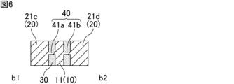
- Fig. 6 is a schematic cross-sectional view showing an example of a cross section taken along line segment b1-b2 of the structure shown in Fig. 5.
- the ceramic material, metal material, and dissipative material are 3D printed using the material jetting method to form the object 1B shown in Figures 5 and 6.
- the object 1B has an electronic component body 10, a support 20, a vanishing body 30, and a connecting body 40.
- the object 1B has a configuration in which the connecting body 40 is provided on the object 1A (see Figures 1 and 2).
- the connector 40 includes a ceramic material.
- the ceramic material contained in the connector 40 is preferably the same as the ceramic material contained in the electronic component body 10 (ceramic portion 11), but may be different from the ceramic material contained in the electronic component body 10 (ceramic portion 11).
- the ceramic material contained in the connector 40 is preferably the same as the ceramic material contained in the support 20, but may be different from the ceramic material contained in the support 20.
- the ceramic material contained in the electronic component body 10 (ceramic portion 11), the ceramic material contained in the support 20, and the ceramic material contained in the connector 40 are preferably the same as each other, but may be different from each other or may be partially different.
- the connector 40 connects the electronic component body 10 and the support 20. In other words, the connector 40 contacts both the electronic component body 10 and the support 20.
- the connector 40 preferably connects the ceramic part 11 and the support 20. In other words, the connector 40 preferably contacts both the ceramic part 11 and the support 20.
- the connector 40 may connect the electrode portion 12 and the support 20. In other words, the connector 40 may be in contact with both the electrode portion 12 and the support 20.
- the connector 40 may be made up of one connector member or multiple connector members.
- the connector 40 is composed of two connectors: a first connector 41a that connects the ceramic part 11 to the third support member 21c, and a second connector 41b that connects the ceramic part 11 to the fourth support member 21d.
- the position of the connector 40 relative to the electronic component body 10 is not particularly limited.
- the positions of the first connector 41a and the second connector 41b relative to the ceramic part 11 are not limited to the positions shown in Figures 5 and 6.
- the position of the connector 40 relative to the support 20 is not particularly limited.
- the position of the first connector 41a relative to the third support 21c and the position of the second connector 41b relative to the fourth support 21d are not limited to the positions shown in Figures 5 and 6.
- the shaped object 1B is fired at a temperature equal to or higher than the temperature at which the vanishing body 30 vanishes. This causes the vanishing body 30 to vanish from the shaped object 1B, and sinters the ceramic material contained in the shaped object 1B, particularly the ceramic material contained in the electronic component body 10.
- the molded object 1B has a connector 40 that connects the electronic component body 10 and the support 20, and the electronic component body 10 is fixed to the support 20 that is provided around at least a portion of the periphery of the electronic component body 10 via the connector 40, so that deformation of the electronic component body 10 during firing is sufficiently suppressed.
- FIG. 7 is a schematic perspective view showing an electronic component body with connectors obtained in the middle of the process of obtaining the electronic component body in the manufacturing method for a ceramic electronic component according to the second embodiment of the present invention.
- an electronic component body 10 with a connector 40 is obtained in a state where the support 20 is separated from the sintered object 1B.
- the connector 40 is removed from the electronic component body 10 with the connector 40 attached, thereby obtaining the electronic component body 10 shown in FIG. 3 as a ceramic electronic component.
- the method for removing the connector 40 is not particularly limited, and examples include cutting, grinding (e.g., blasting), etc. Traces of the connector 40 removed by these methods will remain on the electronic component body 10 (here, the ceramic part 11).
- the shaped object in the step of forming a shaped object, the shaped object may be formed on a printed base, in the step of firing the shaped object, the shaped object may be fired on the printed base, and the shaped object may be separated from the printed base during firing in the step of firing the shaped object.
- the method for producing a ceramic electronic component according to the modified embodiment of the second embodiment of the present invention which is such an example, is similar to the method for producing a ceramic electronic component according to the modified embodiment of the first embodiment of the present invention in that a printed base is used.
- ⁇ 1> a step of 3D printing a ceramic material, a metal material, and a dissipative material by a material jetting method to form a shaped object having an electronic component body including the ceramic material and the metal material, a support body including the ceramic material and provided on at least a portion of the periphery of the electronic component body, and a dissipative body including the dissipative material and provided between the electronic component body and the support body; Firing the shaped object at a temperature equal to or higher than the temperature at which the disappearing body disappears; obtaining the electronic component main body in a state in which the support is separated from the shaped article after firing.
- ⁇ 2> The method for producing a ceramic electronic component according to ⁇ 1>, wherein the electronic component body has an irregular shape and is provided with a recess.
- ⁇ 4> The method for producing a ceramic electronic component according to any one of ⁇ 1> to ⁇ 3>, wherein a volume of the support is larger than a volume of the electronic component body.
- ⁇ 5> The method for producing a ceramic electronic component according to any one of ⁇ 1> to ⁇ 4>, wherein the support body is constituted by a plurality of support members.
- ⁇ 6> The method for producing a ceramic electronic component according to any one of ⁇ 1> to ⁇ 5>, wherein the shaped object includes the ceramic material, and further includes a connector that connects the electronic component body and the support.
- the object is formed on a printing base;
- the object is fired on the printing base, ⁇ 7>
- ⁇ 8> The method for producing a ceramic electronic component according to ⁇ 7>, wherein the printing base has a disappearance portion on a surface thereof that disappears during firing in a step of firing the shaped object.
- ⁇ 9> The method for producing a ceramic electronic component according to ⁇ 8>, wherein a temperature at which the disappearing portion disappears is lower than a temperature at which the disappearing body disappears.
- ⁇ 11> The method for producing a ceramic electronic component according to any one of ⁇ 8> to ⁇ 10>, wherein the printing base further has a support portion having a porous structure and provided so as to be in contact with the disappearance portion.
- Reference Signs 1A, 1B Modeled object 10 Electronic component body 11 Ceramic portion 12 Electrode portion 13a First electrode member 13b Second electrode member 15 Recess 20 Support body 21a First support member 21b Second support member 21c Third support member 21d Fourth support member 30 Vanishing body 40 Connecting body 41a First connecting member 41b Second connecting member 100 Print base 110 Vanishing portion 120 Supporting portion
Landscapes
- Engineering & Computer Science (AREA)
- Manufacturing & Machinery (AREA)
- Chemical & Material Sciences (AREA)
- Mechanical Engineering (AREA)
- Materials Engineering (AREA)
- Power Engineering (AREA)
- Ceramic Engineering (AREA)
- Physics & Mathematics (AREA)
- Optics & Photonics (AREA)
- Microelectronics & Electronic Packaging (AREA)
- Fixed Capacitors And Capacitor Manufacturing Machines (AREA)
Priority Applications (1)
| Application Number | Priority Date | Filing Date | Title |
|---|---|---|---|
| JP2024557343A JPWO2024101211A1 (https=) | 2022-11-09 | 2023-10-31 |
Applications Claiming Priority (2)
| Application Number | Priority Date | Filing Date | Title |
|---|---|---|---|
| JP2022179682 | 2022-11-09 | ||
| JP2022-179682 | 2022-11-09 |
Publications (1)
| Publication Number | Publication Date |
|---|---|
| WO2024101211A1 true WO2024101211A1 (ja) | 2024-05-16 |
Family
ID=91032311
Family Applications (1)
| Application Number | Title | Priority Date | Filing Date |
|---|---|---|---|
| PCT/JP2023/039184 Ceased WO2024101211A1 (ja) | 2022-11-09 | 2023-10-31 | セラミック電子部品の製造方法 |
Country Status (2)
| Country | Link |
|---|---|
| JP (1) | JPWO2024101211A1 (https=) |
| WO (1) | WO2024101211A1 (https=) |
Citations (6)
| Publication number | Priority date | Publication date | Assignee | Title |
|---|---|---|---|---|
| JP2000323328A (ja) * | 1999-05-11 | 2000-11-24 | Murata Mfg Co Ltd | チップインダクタ |
| JP2004255839A (ja) * | 2003-02-28 | 2004-09-16 | Hitachi Printing Solutions Ltd | インクジェット方式の三次元造形装置及びその造形法 |
| JP2018144261A (ja) * | 2017-03-01 | 2018-09-20 | 株式会社ミマキエンジニアリング | 三次元造形装置及び三次元造形方法 |
| JP2020512219A (ja) * | 2017-03-30 | 2020-04-23 | ダウ シリコーンズ コーポレーション | 多孔質三次元(3d)物品を形成する方法 |
| WO2021181561A1 (ja) * | 2020-03-11 | 2021-09-16 | 株式会社Fuji | 3次元積層造形による実装基板の製造方法 |
| JP2021174923A (ja) * | 2020-04-28 | 2021-11-01 | 株式会社村田製作所 | 積層型セラミック電子部品の製造方法および消失性インク |
-
2023
- 2023-10-31 JP JP2024557343A patent/JPWO2024101211A1/ja active Pending
- 2023-10-31 WO PCT/JP2023/039184 patent/WO2024101211A1/ja not_active Ceased
Patent Citations (6)
| Publication number | Priority date | Publication date | Assignee | Title |
|---|---|---|---|---|
| JP2000323328A (ja) * | 1999-05-11 | 2000-11-24 | Murata Mfg Co Ltd | チップインダクタ |
| JP2004255839A (ja) * | 2003-02-28 | 2004-09-16 | Hitachi Printing Solutions Ltd | インクジェット方式の三次元造形装置及びその造形法 |
| JP2018144261A (ja) * | 2017-03-01 | 2018-09-20 | 株式会社ミマキエンジニアリング | 三次元造形装置及び三次元造形方法 |
| JP2020512219A (ja) * | 2017-03-30 | 2020-04-23 | ダウ シリコーンズ コーポレーション | 多孔質三次元(3d)物品を形成する方法 |
| WO2021181561A1 (ja) * | 2020-03-11 | 2021-09-16 | 株式会社Fuji | 3次元積層造形による実装基板の製造方法 |
| JP2021174923A (ja) * | 2020-04-28 | 2021-11-01 | 株式会社村田製作所 | 積層型セラミック電子部品の製造方法および消失性インク |
Also Published As
| Publication number | Publication date |
|---|---|
| JPWO2024101211A1 (https=) | 2024-05-16 |
Similar Documents
| Publication | Publication Date | Title |
|---|---|---|
| JP2000285731A (ja) | 導体ペーストおよびセラミック多層基板の製造方法 | |
| JP4359914B2 (ja) | 積層型電子部品およびその製法 | |
| WO2024101211A1 (ja) | セラミック電子部品の製造方法 | |
| JP2019016688A (ja) | 積層セラミック電子部品の製造方法 | |
| JP2004179388A (ja) | 金属薄膜付セラミックグリーンシートおよびセラミックコンデンサの製造方法 | |
| WO2025211364A1 (ja) | 電子部品の製造方法 | |
| CN101060033B (zh) | 制造电极图案的方法 | |
| JP2023041842A5 (https=) | ||
| JP2023041842A (ja) | 積層型セラミック電子部品の製造方法 | |
| JP4048796B2 (ja) | 多層セラミック基板の製造方法 | |
| JP2003273515A (ja) | セラミックの低温焼結の間の収縮を低減するための方法および抑制層 | |
| TWI908043B (zh) | 配線基板 | |
| JP4084696B2 (ja) | 低温焼成多層セラミック配線基板の製法 | |
| JP2006066626A (ja) | 複合体及び複合体の製造方法並びに、複合シートの製造方法、積層体の製造方法、積層部品の製造方法 | |
| JPH04125990A (ja) | 多層セラミックス回路基板およびその製造方法 | |
| JP2005268300A (ja) | チップ抵抗器およびその製造方法 | |
| JP6065355B2 (ja) | 多層セラミック基板およびその製造方法 | |
| JP4404366B2 (ja) | 多層セラミック基板の製造方法および多層セラミック基板 | |
| JP2004146701A (ja) | ガラスセラミック基板の製造方法 | |
| JP2014011314A (ja) | セラミック基板およびその製造方法 | |
| JP2003283130A (ja) | セラミック多層基板の製造方法 | |
| KR101214691B1 (ko) | 다층 세라믹 기판 및 이의 제조 방법 | |
| JP2004186341A (ja) | セラミック積層体の製法 | |
| JP2018026433A (ja) | セラミック多層基板の製造方法 | |
| WO2019111544A1 (ja) | 集合基板の製造方法、及び、集合基板 |
Legal Events
| Date | Code | Title | Description |
|---|---|---|---|
| 121 | Ep: the epo has been informed by wipo that ep was designated in this application |
Ref document number: 23888559 Country of ref document: EP Kind code of ref document: A1 |
|
| WWE | Wipo information: entry into national phase |
Ref document number: 2024557343 Country of ref document: JP |
|
| NENP | Non-entry into the national phase |
Ref country code: DE |
|
| 122 | Ep: pct application non-entry in european phase |
Ref document number: 23888559 Country of ref document: EP Kind code of ref document: A1 |