WO2024096070A1 - 縦型半導体装置 - Google Patents
縦型半導体装置 Download PDFInfo
- Publication number
- WO2024096070A1 WO2024096070A1 PCT/JP2023/039460 JP2023039460W WO2024096070A1 WO 2024096070 A1 WO2024096070 A1 WO 2024096070A1 JP 2023039460 W JP2023039460 W JP 2023039460W WO 2024096070 A1 WO2024096070 A1 WO 2024096070A1
- Authority
- WO
- WIPO (PCT)
- Prior art keywords
- layer
- region
- trench
- base layer
- contact
- Prior art date
- Legal status (The legal status is an assumption and is not a legal conclusion. Google has not performed a legal analysis and makes no representation as to the accuracy of the status listed.)
- Ceased
Links
Images


Classifications
-
- H—ELECTRICITY
- H10—SEMICONDUCTOR DEVICES; ELECTRIC SOLID-STATE DEVICES NOT OTHERWISE PROVIDED FOR
- H10D—INORGANIC ELECTRIC SEMICONDUCTOR DEVICES
- H10D30/00—Field-effect transistors [FET]
- H10D30/60—Insulated-gate field-effect transistors [IGFET]
- H10D30/64—Double-diffused metal-oxide semiconductor [DMOS] FETs
- H10D30/66—Vertical DMOS [VDMOS] FETs
- H10D30/665—Vertical DMOS [VDMOS] FETs having edge termination structures
-
- H—ELECTRICITY
- H10—SEMICONDUCTOR DEVICES; ELECTRIC SOLID-STATE DEVICES NOT OTHERWISE PROVIDED FOR
- H10D—INORGANIC ELECTRIC SEMICONDUCTOR DEVICES
- H10D12/00—Bipolar devices controlled by the field effect, e.g. insulated-gate bipolar transistors [IGBT]
-
- H—ELECTRICITY
- H10—SEMICONDUCTOR DEVICES; ELECTRIC SOLID-STATE DEVICES NOT OTHERWISE PROVIDED FOR
- H10D—INORGANIC ELECTRIC SEMICONDUCTOR DEVICES
- H10D30/00—Field-effect transistors [FET]
- H10D30/60—Insulated-gate field-effect transistors [IGFET]
- H10D30/64—Double-diffused metal-oxide semiconductor [DMOS] FETs
- H10D30/66—Vertical DMOS [VDMOS] FETs
- H10D30/668—Vertical DMOS [VDMOS] FETs having trench gate electrodes, e.g. UMOS transistors
-
- H—ELECTRICITY
- H10—SEMICONDUCTOR DEVICES; ELECTRIC SOLID-STATE DEVICES NOT OTHERWISE PROVIDED FOR
- H10D—INORGANIC ELECTRIC SEMICONDUCTOR DEVICES
- H10D62/00—Semiconductor bodies, or regions thereof, of devices having potential barriers
- H10D62/10—Shapes, relative sizes or dispositions of the regions of the semiconductor bodies; Shapes of the semiconductor bodies
- H10D62/102—Constructional design considerations for preventing surface leakage or controlling electric field concentration
- H10D62/103—Constructional design considerations for preventing surface leakage or controlling electric field concentration for increasing or controlling the breakdown voltage of reverse-biased devices
- H10D62/105—Constructional design considerations for preventing surface leakage or controlling electric field concentration for increasing or controlling the breakdown voltage of reverse-biased devices by having particular doping profiles, shapes or arrangements of PN junctions; by having supplementary regions, e.g. junction termination extension [JTE]
-
- H—ELECTRICITY
- H10—SEMICONDUCTOR DEVICES; ELECTRIC SOLID-STATE DEVICES NOT OTHERWISE PROVIDED FOR
- H10D—INORGANIC ELECTRIC SEMICONDUCTOR DEVICES
- H10D62/00—Semiconductor bodies, or regions thereof, of devices having potential barriers
- H10D62/10—Shapes, relative sizes or dispositions of the regions of the semiconductor bodies; Shapes of the semiconductor bodies
- H10D62/13—Semiconductor regions connected to electrodes carrying current to be rectified, amplified or switched, e.g. source or drain regions
- H10D62/149—Source or drain regions of field-effect devices
- H10D62/151—Source or drain regions of field-effect devices of IGFETs
- H10D62/152—Source regions of DMOS transistors
- H10D62/153—Impurity concentrations or distributions
-
- H—ELECTRICITY
- H10—SEMICONDUCTOR DEVICES; ELECTRIC SOLID-STATE DEVICES NOT OTHERWISE PROVIDED FOR
- H10D—INORGANIC ELECTRIC SEMICONDUCTOR DEVICES
- H10D62/00—Semiconductor bodies, or regions thereof, of devices having potential barriers
- H10D62/60—Impurity distributions or concentrations
-
- H—ELECTRICITY
- H10—SEMICONDUCTOR DEVICES; ELECTRIC SOLID-STATE DEVICES NOT OTHERWISE PROVIDED FOR
- H10D—INORGANIC ELECTRIC SEMICONDUCTOR DEVICES
- H10D64/00—Electrodes of devices having potential barriers
- H10D64/20—Electrodes characterised by their shapes, relative sizes or dispositions
- H10D64/23—Electrodes carrying the current to be rectified, amplified, oscillated or switched, e.g. sources, drains, anodes or cathodes
- H10D64/251—Source or drain electrodes for field-effect devices
- H10D64/252—Source or drain electrodes for field-effect devices for vertical or pseudo-vertical devices
- H10D64/2527—Source or drain electrodes for field-effect devices for vertical or pseudo-vertical devices for vertical devices wherein the source or drain electrodes are recessed in semiconductor bodies
-
- H—ELECTRICITY
- H10—SEMICONDUCTOR DEVICES; ELECTRIC SOLID-STATE DEVICES NOT OTHERWISE PROVIDED FOR
- H10D—INORGANIC ELECTRIC SEMICONDUCTOR DEVICES
- H10D84/00—Integrated devices formed in or on semiconductor substrates that comprise only semiconducting layers, e.g. on Si wafers or on GaAs-on-Si wafers
- H10D84/101—Integrated devices comprising main components and built-in components, e.g. IGBT having built-in freewheel diode
- H10D84/141—VDMOS having built-in components
-
- H—ELECTRICITY
- H10—SEMICONDUCTOR DEVICES; ELECTRIC SOLID-STATE DEVICES NOT OTHERWISE PROVIDED FOR
- H10D—INORGANIC ELECTRIC SEMICONDUCTOR DEVICES
- H10D12/00—Bipolar devices controlled by the field effect, e.g. insulated-gate bipolar transistors [IGBT]
- H10D12/01—Manufacture or treatment
- H10D12/031—Manufacture or treatment of IGBTs
- H10D12/032—Manufacture or treatment of IGBTs of vertical IGBTs
- H10D12/038—Manufacture or treatment of IGBTs of vertical IGBTs having a recessed gate, e.g. trench-gate IGBTs
-
- H—ELECTRICITY
- H10—SEMICONDUCTOR DEVICES; ELECTRIC SOLID-STATE DEVICES NOT OTHERWISE PROVIDED FOR
- H10D—INORGANIC ELECTRIC SEMICONDUCTOR DEVICES
- H10D12/00—Bipolar devices controlled by the field effect, e.g. insulated-gate bipolar transistors [IGBT]
- H10D12/411—Insulated-gate bipolar transistors [IGBT]
- H10D12/415—Insulated-gate bipolar transistors [IGBT] having edge termination structures
-
- H—ELECTRICITY
- H10—SEMICONDUCTOR DEVICES; ELECTRIC SOLID-STATE DEVICES NOT OTHERWISE PROVIDED FOR
- H10D—INORGANIC ELECTRIC SEMICONDUCTOR DEVICES
- H10D12/00—Bipolar devices controlled by the field effect, e.g. insulated-gate bipolar transistors [IGBT]
- H10D12/411—Insulated-gate bipolar transistors [IGBT]
- H10D12/441—Vertical IGBTs
- H10D12/461—Vertical IGBTs having non-planar surfaces, e.g. having trenches, recesses or pillars in the surfaces of the emitter, base or collector regions
- H10D12/481—Vertical IGBTs having non-planar surfaces, e.g. having trenches, recesses or pillars in the surfaces of the emitter, base or collector regions having gate structures on slanted surfaces, on vertical surfaces, or in grooves, e.g. trench gate IGBTs
-
- H—ELECTRICITY
- H10—SEMICONDUCTOR DEVICES; ELECTRIC SOLID-STATE DEVICES NOT OTHERWISE PROVIDED FOR
- H10D—INORGANIC ELECTRIC SEMICONDUCTOR DEVICES
- H10D62/00—Semiconductor bodies, or regions thereof, of devices having potential barriers
- H10D62/10—Shapes, relative sizes or dispositions of the regions of the semiconductor bodies; Shapes of the semiconductor bodies
- H10D62/124—Shapes, relative sizes or dispositions of the regions of semiconductor bodies or of junctions between the regions
- H10D62/126—Top-view geometrical layouts of the regions or the junctions
- H10D62/127—Top-view geometrical layouts of the regions or the junctions of cellular field-effect devices, e.g. multicellular DMOS transistors or IGBTs
Definitions
- This disclosure relates to a vertical semiconductor device having a trench gate structure.
- this vertical semiconductor device is configured by forming a MOSFET (short for metal oxide semiconductor field effect transistor). More specifically, in the vertical semiconductor device, an n- type drift layer is formed on an n + type drain region, and a p-type base layer is formed on the drift layer. An n + type source layer is formed on the surface layer of the base layer, and the trench gate structure is formed so as to penetrate the source layer and the base layer and reach the drift layer.
- MOSFET metal oxide semiconductor field effect transistor
- Such a vertical semiconductor device usually includes a cell region in which a MOSFET element is formed, and a peripheral region surrounding the cell region, and the trench gate structure may be extended from the cell region to the peripheral region so as to reduce the electric field in the peripheral region.
- a parasitic bipolar transistor is formed by the drift layer, the base layer, and the source layer. According to the study by the present inventors, when the trench gate structure is extended to the peripheral region, it has been confirmed that the parasitic bipolar transistor is likely to operate around the trench gate structure arranged in the peripheral region. For this reason, it is desired to improve the avalanche resistance so that the parasitic bipolar transistor is less likely to operate.
- the purpose of this disclosure is to provide a vertical semiconductor device that can improve avalanche resistance.
- a vertical semiconductor device in which a semiconductor element having a trench gate structure is formed includes a semiconductor substrate having a cell region in which the semiconductor element is formed and an outer periphery region surrounding the cell region, and the cell region includes a drift layer of a first conductivity type, a base layer of a second conductivity type formed on the drift layer, an impurity layer of the first conductivity type formed in a surface layer portion of the base layer and having a higher impurity concentration than the drift layer, a trench gate structure in which a gate electrode is disposed via a gate insulating film in a trench extending along the surface direction of the semiconductor substrate through the impurity layer and the base layer and reaching the drift layer, and a gate insulating film formed on the opposite side of the base layer across the drift layer and having a higher impurity concentration than the drift layer.
- the semiconductor device has a high-concentration layer of a first or second conductivity type having a higher impurity concentration than the first or second conductivity type, an interlayer insulating film formed on one surface of the semiconductor substrate and having a contact hole that exposes the base layer and the impurity layer, a first electrode electrically connected to the impurity layer and the base layer through the contact hole, and a second electrode electrically connected to the high-concentration layer, the region in which the impurity layer is formed is the cell region, the trench gate structure extends from the cell region to the peripheral region, the base layer extends from the cell region to the peripheral region, the contact hole extends from the cell region to the peripheral region, and the first electrode is connected to the base layer through the contact hole even in the peripheral region.
- FIG. 1 is a plan view of a vertical semiconductor device according to a first embodiment
- 2 is a cross-sectional view taken along line II-II in FIG. 1.
- FIG. 2 is a cross-sectional view taken along line III-III in FIG. 2 is a schematic diagram showing a circuit configuration of the vertical semiconductor device shown in FIG. 1 .
- FIG. 13 is a diagram showing the relationship between the adjustment distance and the avalanche resistance.
- FIG. 11 is a cross-sectional view of a vertical semiconductor device according to a second embodiment.
- a vertical semiconductor device according to a first embodiment of the present invention is preferably mounted on a vehicle such as an automobile and used as a device for driving various electronic devices for the vehicle.
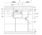
- the vertical semiconductor device of this embodiment has a cell region 1 and a peripheral region 2.
- the vertical semiconductor device of this embodiment is configured by forming an n-channel MOSFET element having a source layer 14 as a semiconductor element.
- the cell region 1 and the peripheral region 2 are divided depending on whether the source layer 14 is formed or not, and the part where the source layer 14 is formed is the cell region 1.
- the part that actually functions as a MOSFET element is the cell region 1
- the part that does not function as a MOSFET element is the peripheral region 2.
- the interlayer insulating film 20 and the upper electrode 21 described later are omitted.
- FIG. 1 is not a cross-sectional view, the gate insulating film 17 and the gate electrode 18 described later are hatched to make it easier to understand.
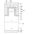
- the vertical semiconductor device of this embodiment is formed using a semiconductor substrate 10 having a substrate 11 composed of an n + type silicon substrate or the like having a high impurity concentration.
- An n- type drift layer 12 having a lower impurity concentration than the substrate 11 is formed on the surface of the substrate 11.
- the substrate 11 functions as a drain region and corresponds to a high concentration layer.
- a p-type base layer 13 having a relatively low impurity concentration is formed on the surface layer of the drift layer 12.
- the base layer 13 is formed, for example, by ion implantation of p-type impurities into the drift layer 12, and functions as a channel layer that forms a channel region.
- the base layer 13 includes a base region 13a located on the drift layer 12 side, and a base contact region 13b formed on the base region 13a and having a higher impurity concentration than the base region 13a.
- the base layer 13 in this embodiment is formed from the cell region 1 to the outer periphery region 2.
- n + type source layer 14 having a higher impurity concentration than the drift layer 12 is formed in a surface layer portion of the base layer 13.
- the source layer 14 is formed between a plurality of trenches 16 described later so as to contact the side of the trench 16.
- the base contact region 13b is formed so as to be located on the opposite side of the trench 16 described later with the source layer 14 in between.
- the region in which the source layer 14 is formed is the cell region 1.
- the base contact region 13b may be formed to coincide with the source layer 14 in the longitudinal direction (i.e., extension direction) of the trench 16 described below, or may be formed to protrude slightly from the cell region 1 to the outer periphery region 2.
- the source layer 14 corresponds to the impurity layer.
- the semiconductor substrate 10 has the substrate 11 side as the other surface 10b, and the base layer 13 and source layer 14 side as the first surface 10a.
- a plurality of trenches 16 are formed so as to penetrate from the one surface 10a side through the base layer 13 and the source layer 14 to reach the drift layer 12.
- the plurality of trenches 16 are formed so as to be arranged along a direction intersecting one direction in the surface direction of the semiconductor substrate 10 as the longitudinal direction. More specifically, the plurality of trenches 16 are arranged in parallel at equal intervals to form a striped layout.
- the trenches 16 are arranged so that the longitudinal direction is the left-right direction of the paper and are arranged in the up-down direction of the paper.
- each trench 16 is formed so that both ends in the longitudinal direction protrude from the cell region 1 to the outer periphery region 2.
- the inner wall surface of the trench 16 is covered with a gate insulating film 17.
- a gate electrode 18 made of doped polysilicon is disposed within the trench 16 via the gate insulating film 17.
- an interlayer insulating film 20 made of an oxide film or the like is formed so as to cover the gate electrode 18.
- contact holes 20a are formed in the interlayer insulating film 20 to expose the source layer 14 and the base layer 13.
- the contact hole 20a is formed so as to protrude beyond the source layer 14 in the longitudinal direction of the trench 16.
- the contact hole 20a is formed so as to also expose the base layer 13 located in the peripheral region 2.
- the contact hole 20a is formed so as to terminate closer to the cell region 1 side than the longitudinal end of the trench 16.
- the contact hole 20a is indicated by a dotted line.
- the area surrounded by the dotted line is the area exposed from the interlayer insulating film 20.
- An upper electrode 21 equivalent to a source electrode is formed on the interlayer insulating film 20. Specifically, the upper electrode 21 is formed in the cell region 1 so as to be connected to the source layer 14 and the base contact region 13b (i.e., the base layer 13) through the contact hole 20a. The upper electrode 21 is also formed in the peripheral region 2 so as to be connected to the base layer 13 through the contact hole 20a. In this embodiment, the upper electrode 21 corresponds to the first electrode.
- the lower electrode 22 corresponds to the second electrode.
- the n - type, n-type, and n + type correspond to the first conductivity type
- the p-type and p + type correspond to the second conductivity type
- the semiconductor substrate 10 is configured to include the substrate 11, drift layer 12, base layer 13, source layer 14, etc., as described above.
- a voltage equal to or greater than the threshold voltage of the insulated gate structure is applied to the gate electrode 18, whereby a channel region is formed in the base layer 13 that contacts the trench 16, and a current flows between the source and drain, turning the device into an ON state. Furthermore, when the voltage applied to the gate electrode 18 becomes less than the threshold voltage, the channel region formed in the base layer 13 disappears, and the current is cut off, turning the device into an OFF state.
- the vertical semiconductor device described above has a circuit configuration as shown in FIG. 4. That is, the vertical semiconductor device in this embodiment has a circuit configuration including a MOS transistor MTr, a drift layer 12, a base layer 13, a parasitic bipolar transistor PTr formed by a source layer 14, a depletion capacitance DC, and an internal resistance R of the base layer 13.
- a vertical semiconductor device such as the above, when switching from an on state to an off state, avalanche breakdown may occur, causing an excessive current to flow between the source and drain.
- the contact hole 20a is extended to the peripheral region 2, and the base layer 13 is electrically connected to the upper electrode 21 in the peripheral region 2.
- the vertical semiconductor device performs avalanche operation, holes are easily extracted from the upper electrode 21 through the base layer 13 in the peripheral region 2.
- the region where the internal resistance R of the base layer 13 is small increases. Therefore, the avalanche resistance can be improved, and the operation of the parasitic bipolar transistor PTr can be suppressed.
- the length of the contact hole 20a protruding from the cell region 1 to the peripheral region 2 is set as the adjustment distance d.
- the length of the contact hole 20a protruding from the source layer 14 to the peripheral region 2 is set as the adjustment distance d.
- the length along the longitudinal direction of the trench 16 of the base layer 13 connected to the upper electrode 21 in the peripheral region 2 is set as the adjustment distance d.
- the longer the adjustment distance d the easier it is to extract holes from the upper electrode 21.
- the adjustment distance d is set to 0.1 ⁇ m or more.
- FIG. 5 shows the results for each impurity concentration, with the substrate 11 at 1 ⁇ 10 to 1 ⁇ 10 cm ⁇ 3 , the drift layer 12 at 1 ⁇ 10 to 1 ⁇ 10 cm ⁇ 3 , the base region 13a at 1 ⁇ 10 cm ⁇ 3 , the base contact region 13b at approximately 1 ⁇ 10 to 1 ⁇ 10 cm ⁇ 3 , and the source layer 14 at approximately 1 ⁇ 10 cm ⁇ 3 .
- the contact hole 20a extends from the cell region 1 to the peripheral region 2, and the upper electrode 21 is connected to the base layer 13 even in the peripheral region 2. Therefore, when the vertical semiconductor device performs an avalanche operation, holes are easily extracted from the upper electrode 21 through the base layer 13 in the peripheral region 2. This makes it possible to improve the avalanche resistance and suppress the operation of the parasitic bipolar transistor PTr.
- the adjustment distance is set to 0.1 ⁇ m or more. This allows the avalanche resistance to be sufficiently high.
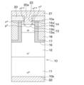
- Second Embodiment A second embodiment will be described. This embodiment differs from the first embodiment in that a trench contact is formed. As the rest is similar to the first embodiment, a description thereof will be omitted here.
- a contact trench 23 is formed in the semiconductor substrate 10 so as to communicate with the contact hole 20a formed in the interlayer insulating film 20. More specifically, the contact trench 23 is formed so as to coincide with the contact hole 20a in the normal direction to the one surface 10a of the semiconductor substrate 10. In other words, the contact trench 23 has an adjustment distance d from the cell region 1 of 0.1 ⁇ m or more, similar to the contact hole 20a.
- the source layer 14 in this embodiment has a source region 14a located on the gate insulating film 17 side, and a source contact region 14b that has a higher impurity concentration than the source layer 14 and is formed so as to contact the side surface of the contact trench 23.
- the base contact region 13b is formed so as to contact the bottom surface of the contact trench 23.
- the contact hole 20a extends from the cell region 1 to the peripheral region 2, and the upper electrode 21 is connected to the base layer 13 even in the peripheral region 2. Therefore, the same effect as in the first embodiment can be obtained.
- the contact hole 20a and contact trench 23 not to extend to the peripheral region 2, but to form a separate contact hole in the peripheral region 2 to connect the upper electrode 21 to the base layer 13 in the peripheral region 2.
- the process of forming the contact trench 23 and contact hole 20a and the process of forming the separate contact hole must be performed separately, which increases the number of manufacturing steps.
- the vertical semiconductor device of this embodiment can achieve the same effects as the first embodiment while suppressing an increase in the number of manufacturing steps.
- a contact trench 23 is formed in the semiconductor substrate 10, and the source contact region 14b and the base contact region 13b are formed so as to be in contact with the contact trench 23. This makes it easier to ensure the connection area with the upper electrode 21, and shortens the length between adjacent trenches 16. This allows the on-resistance to be reduced, and the vertical semiconductor device to be made smaller.
- an n-channel type trench gate MOSFET in which the first conductivity type is n-type and the second conductivity type is p-type has been described as an example.
- the vertical semiconductor device may be configured by forming a p-channel type trench gate MOSFET in which the conductivity types of each component are inverted with respect to the n-channel type.
- the vertical semiconductor device may be configured by forming an IGBT having a similar structure in addition to the MOSFET. In the case of the IGBT, it is the same as the vertical MOSFET described in the first embodiment, except that the n + type substrate 11 in each of the above embodiments is changed to a p + type collector layer.
- the semiconductor substrate 10 is configured as a silicon substrate.
- the semiconductor substrate 10 may be a silicon carbide substrate or a gallium nitride substrate.
- the base contact region 13b may not be formed, and the base layer 13 may be directly connected to the upper electrode 21.
- the source contact region 14b may be formed so as to be connected to the upper electrode 21, and in the second embodiment, the source contact region 14b may not be formed.
Landscapes
- Electrodes Of Semiconductors (AREA)
Priority Applications (2)
| Application Number | Priority Date | Filing Date | Title |
|---|---|---|---|
| CN202380076082.5A CN120240003A (zh) | 2022-11-02 | 2023-11-01 | 纵型半导体装置 |
| US19/192,895 US20250261439A1 (en) | 2022-11-02 | 2025-04-29 | Vertical semiconductor device |
Applications Claiming Priority (2)
| Application Number | Priority Date | Filing Date | Title |
|---|---|---|---|
| JP2022-176618 | 2022-11-02 | ||
| JP2022176618A JP2024066860A (ja) | 2022-11-02 | 2022-11-02 | 縦型半導体装置 |
Related Child Applications (1)
| Application Number | Title | Priority Date | Filing Date |
|---|---|---|---|
| US19/192,895 Continuation-In-Part US20250261439A1 (en) | 2022-11-02 | 2025-04-29 | Vertical semiconductor device |
Publications (1)
| Publication Number | Publication Date |
|---|---|
| WO2024096070A1 true WO2024096070A1 (ja) | 2024-05-10 |
Family
ID=90930659
Family Applications (1)
| Application Number | Title | Priority Date | Filing Date |
|---|---|---|---|
| PCT/JP2023/039460 Ceased WO2024096070A1 (ja) | 2022-11-02 | 2023-11-01 | 縦型半導体装置 |
Country Status (4)
| Country | Link |
|---|---|
| US (1) | US20250261439A1 (https=) |
| JP (1) | JP2024066860A (https=) |
| CN (1) | CN120240003A (https=) |
| WO (1) | WO2024096070A1 (https=) |
Citations (3)
| Publication number | Priority date | Publication date | Assignee | Title |
|---|---|---|---|---|
| JP2019087730A (ja) * | 2017-11-08 | 2019-06-06 | 富士電機株式会社 | 半導体装置 |
| JP2020098820A (ja) * | 2018-12-17 | 2020-06-25 | 三菱電機株式会社 | 半導体装置 |
| JP2022038240A (ja) * | 2020-08-26 | 2022-03-10 | 株式会社デンソー | 半導体装置 |
-
2022
- 2022-11-02 JP JP2022176618A patent/JP2024066860A/ja active Pending
-
2023
- 2023-11-01 CN CN202380076082.5A patent/CN120240003A/zh active Pending
- 2023-11-01 WO PCT/JP2023/039460 patent/WO2024096070A1/ja not_active Ceased
-
2025
- 2025-04-29 US US19/192,895 patent/US20250261439A1/en active Pending
Patent Citations (3)
| Publication number | Priority date | Publication date | Assignee | Title |
|---|---|---|---|---|
| JP2019087730A (ja) * | 2017-11-08 | 2019-06-06 | 富士電機株式会社 | 半導体装置 |
| JP2020098820A (ja) * | 2018-12-17 | 2020-06-25 | 三菱電機株式会社 | 半導体装置 |
| JP2022038240A (ja) * | 2020-08-26 | 2022-03-10 | 株式会社デンソー | 半導体装置 |
Also Published As
| Publication number | Publication date |
|---|---|
| CN120240003A (zh) | 2025-07-01 |
| JP2024066860A (ja) | 2024-05-16 |
| US20250261439A1 (en) | 2025-08-14 |
Similar Documents
| Publication | Publication Date | Title |
|---|---|---|
| JP6416142B2 (ja) | 半導体装置 | |
| WO2014163058A1 (ja) | 半導体装置 | |
| JP2007067181A (ja) | 横型二重拡散型電界効果トランジスタおよびそれを備えた集積回路 | |
| JP5795452B1 (ja) | 炭化ケイ素半導体装置、炭化ケイ素半導体装置の製造方法及び炭化ケイ素半導体装置の設計方法 | |
| US12439620B2 (en) | Semiconductor device | |
| CN105723505A (zh) | 半导体装置及半导体装置的制造方法 | |
| JP2009164460A (ja) | 半導体装置 | |
| US9112016B2 (en) | Semiconductor device and method of fabricating the same | |
| JP2002026315A (ja) | 半導体装置 | |
| JP7352360B2 (ja) | 半導体装置 | |
| JP2019004091A (ja) | 半導体装置および半導体装置の製造方法 | |
| WO2024096070A1 (ja) | 縦型半導体装置 | |
| JP6177300B2 (ja) | 半導体装置 | |
| JP6840300B1 (ja) | 炭化珪素半導体装置 | |
| JP7786107B2 (ja) | 半導体装置 | |
| JP2023062308A (ja) | 半導体装置およびその製造方法 | |
| JP7702901B2 (ja) | 半導体装置 | |
| JP6445990B2 (ja) | 半導体装置 | |
| JP7619168B2 (ja) | 半導体装置 | |
| US20250107142A1 (en) | Semiconductor device | |
| JP5339789B2 (ja) | 半導体装置 | |
| JP3873714B2 (ja) | 半導体装置 | |
| JP2000252463A (ja) | 横型mos素子を含む半導体装置 | |
| JP2025104940A (ja) | 半導体装置 | |
| JP2025104939A (ja) | 半導体装置 |
Legal Events
| Date | Code | Title | Description |
|---|---|---|---|
| 121 | Ep: the epo has been informed by wipo that ep was designated in this application |
Ref document number: 23885824 Country of ref document: EP Kind code of ref document: A1 |
|
| WWE | Wipo information: entry into national phase |
Ref document number: 202380076082.5 Country of ref document: CN |
|
| NENP | Non-entry into the national phase |
Ref country code: DE |
|
| WWP | Wipo information: published in national office |
Ref document number: 202380076082.5 Country of ref document: CN |
|
| 122 | Ep: pct application non-entry in european phase |
Ref document number: 23885824 Country of ref document: EP Kind code of ref document: A1 |