WO2024048066A1 - 電力変換装置 - Google Patents
電力変換装置 Download PDFInfo
- Publication number
- WO2024048066A1 WO2024048066A1 PCT/JP2023/024793 JP2023024793W WO2024048066A1 WO 2024048066 A1 WO2024048066 A1 WO 2024048066A1 JP 2023024793 W JP2023024793 W JP 2023024793W WO 2024048066 A1 WO2024048066 A1 WO 2024048066A1
- Authority
- WO
- WIPO (PCT)
- Prior art keywords
- phase
- capacitor
- semiconductor module
- conversion device
- power conversion
- Prior art date
- Legal status (The legal status is an assumption and is not a legal conclusion. Google has not performed a legal analysis and makes no representation as to the accuracy of the status listed.)
- Ceased
Links
Images


Classifications
-
- H—ELECTRICITY
- H05—ELECTRIC TECHNIQUES NOT OTHERWISE PROVIDED FOR
- H05K—PRINTED CIRCUITS; CASINGS OR CONSTRUCTIONAL DETAILS OF ELECTRIC APPARATUS; MANUFACTURE OF ASSEMBLAGES OF ELECTRICAL COMPONENTS
- H05K7/00—Constructional details common to different types of electric apparatus
- H05K7/14—Mounting supporting structure in casing or on frame or rack
- H05K7/1422—Printed circuit boards receptacles, e.g. stacked structures, electronic circuit modules or box like frames
- H05K7/1427—Housings
- H05K7/1432—Housings specially adapted for power drive units or power converters
-
- H—ELECTRICITY
- H05—ELECTRIC TECHNIQUES NOT OTHERWISE PROVIDED FOR
- H05K—PRINTED CIRCUITS; CASINGS OR CONSTRUCTIONAL DETAILS OF ELECTRIC APPARATUS; MANUFACTURE OF ASSEMBLAGES OF ELECTRICAL COMPONENTS
- H05K7/00—Constructional details common to different types of electric apparatus
- H05K7/20—Modifications to facilitate cooling, ventilating, or heating
- H05K7/2089—Modifications to facilitate cooling, ventilating, or heating for power electronics, e.g. for inverters for controlling motor
- H05K7/20909—Forced ventilation, e.g. on heat dissipaters coupled to components
-
- H—ELECTRICITY
- H02—GENERATION; CONVERSION OR DISTRIBUTION OF ELECTRIC POWER
- H02M—APPARATUS FOR CONVERSION BETWEEN AC AND AC, BETWEEN AC AND DC, OR BETWEEN DC AND DC, AND FOR USE WITH MAINS OR SIMILAR POWER SUPPLY SYSTEMS; CONVERSION OF DC OR AC INPUT POWER INTO SURGE OUTPUT POWER; CONTROL OR REGULATION THEREOF
- H02M7/00—Conversion of AC power input into DC power output; Conversion of DC power input into AC power output
- H02M7/42—Conversion of DC power input into AC power output without possibility of reversal
- H02M7/44—Conversion of DC power input into AC power output without possibility of reversal by static converters
- H02M7/48—Conversion of DC power input into AC power output without possibility of reversal by static converters using discharge tubes with control electrode or semiconductor devices with control electrode
-
- H—ELECTRICITY
- H05—ELECTRIC TECHNIQUES NOT OTHERWISE PROVIDED FOR
- H05K—PRINTED CIRCUITS; CASINGS OR CONSTRUCTIONAL DETAILS OF ELECTRIC APPARATUS; MANUFACTURE OF ASSEMBLAGES OF ELECTRICAL COMPONENTS
- H05K7/00—Constructional details common to different types of electric apparatus
- H05K7/20—Modifications to facilitate cooling, ventilating, or heating
- H05K7/2089—Modifications to facilitate cooling, ventilating, or heating for power electronics, e.g. for inverters for controlling motor
Definitions
- the present disclosure relates to a power conversion device.
- a capacitor electrically connected between an input-side semiconductor element and an output-side semiconductor element is mounted on a different substrate from the substrates on which the input-side and output-side semiconductor elements are mounted.
- a power converter device in which a board on which a capacitor is mounted is removable from a board on which a semiconductor element is mounted. In such a power conversion device, by attaching and removing the board on which the capacitor is mounted to the board on which the semiconductor element is mounted, the capacitor is mounted on the same board as the semiconductor element. , the capacitor can be easily replaced.
- Patent Document 1 a board on which a plurality of capacitors are mounted is removably connected to a power supply board on which a power supply is mounted via a connector.
- the capacitor board is supported by the power supply board in a cantilevered state by a connector.
- the capacitor board has a part connected to the power supply board via a connector and a part protruding outward from the part, and the capacitor is mounted on the latter part. Therefore, stress is applied to the connection between the connector and the capacitor board, which may cause a connection failure between the capacitor and electronic components such as a power supply mounted on the power supply board.
- the main objective of the present disclosure is to provide a power conversion device in which the capacitor is easy to replace and in which poor connection between the capacitor and other electronic components is less likely to occur.
- a power conversion device includes a printed circuit board having a first surface, at least one capacitor mounted on the first surface of the printed circuit board, and at least one capacitor mounted in a first direction along the first surface.
- An input-side semiconductor module and an output-side semiconductor module are arranged to sandwich each other and are electrically connected to each other via at least one capacitor.
- the printed circuit board is removably supported by each of the input-side semiconductor module and the output-side semiconductor module.
- FIG. 1 is a circuit diagram of a power conversion device according to Embodiment 1.
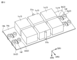
- FIG. 1 is a perspective view of a power conversion device according to Embodiment 1.
- FIG. 1 is a side view of a power conversion device according to Embodiment 1.
- FIG. 2 is a perspective view showing a capacitor and a printed circuit board of the power conversion device according to the first embodiment.
- FIG. 3 is a circuit diagram of a modification of the power conversion device according to Embodiment 1.
- FIG. 7 is a side view of another modification of the power conversion device according to Embodiment 1.
- FIG. FIG. 3 is a cross-sectional view showing a first conductor pattern of a printed circuit board of a power conversion device according to a second embodiment.
- FIG. 7 is a cross-sectional view showing a second conductor pattern of a printed circuit board of a power conversion device according to a second embodiment.
- FIG. FIG. 3 is a side view of a power conversion device according to a third embodiment.
- FIG. 7 is a side view of a power conversion device according to a fourth embodiment.
- FIG. 7 is a side view of a power conversion device according to a fifth embodiment.
- FIG. 7 is a perspective view showing a capacitor and a printed circuit board of a power conversion device according to a fifth embodiment.
- Embodiment 1 ⁇ Configuration of power converter> As shown in FIG. 1, power converter 100 according to the first embodiment is configured as a three-phase power converter.
- the power conversion device 100 includes a first phase unit group 1U, a second phase unit group 1V, and a third phase unit group 1W.
- the first phase unit group 1U, the second phase unit group 1V, and the third phase unit group 1W are configured to perform input and output of the U phase, V phase, and W phase, respectively.
- Each of the first phase unit group 1U, the second phase unit group 1V, and the third phase unit group 1W includes a plurality of power inverter circuit units.
- Each of the plurality of power conversion circuit units includes a plurality of electronic components that constitute the power conversion circuit.
- the first phase unit group 1U, the second phase unit group 1V, and the third phase unit group 1W have the same configuration.
- the first phase unit group 1U will be described as a representative of the first phase unit group 1U, the second phase unit group 1V, and the third phase unit group 1W.
- the first phase unit group 1U includes a first phase first power inverter circuit unit 1U1, a first phase second power inverter circuit unit 1U2, and a first phase third power inverter circuit unit 1U3. including.
- the components of the first phase first power inverter circuit unit 1U1 are surrounded by broken lines.
- the components of the first phase second power inverter circuit unit 1U2 are surrounded by a dashed line.
- the components of the first-phase third power inverter circuit unit 1U3 are surrounded by two-dot chain lines.
- Each of the first phase first power inverter circuit unit 1U1, the first phase second power inverter circuit unit 1U2, and the first phase third power inverter circuit unit 1U3 is configured as a one-phase, one-parallel power inverter circuit unit. ing.
- the first phase first power inverter circuit unit 1U1, the first phase second power inverter circuit unit 1U2, and the first phase third power inverter circuit unit 1U3 are connected in parallel to each other.
- the number of parallel power inverter circuit units can be arbitrarily selected according to the specifications of the power converter device 100.
- the number of parallel power inverter circuit units for each phase may be two, for example.
- the first phase unit group 1U may include a first phase first power inverter circuit unit 1U1 and a first phase second power inverter circuit unit 1U2 that are connected in parallel to each other.
- each of the first phase first power inverter circuit unit 1U1, the first phase second power inverter circuit unit 1U2, and the first phase third power inverter circuit unit 1U3 have the same configuration.
- each power inverter circuit unit of the first phase unit group 1U, the second phase unit group 1V, and the third phase unit group 1W has the same configuration.
- the first phase first power inverter circuit unit 1U1 will be described as a representative of each of the power inverter circuit units of the first phase unit group 1U, the second phase unit group 1V, and the third phase unit group 1W.
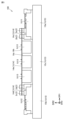
- the first phase first power inverter circuit unit 1U1 includes, for example, a first input side semiconductor module 1U11, a first output side semiconductor module 1U12, and a plurality of first phase first capacitors 1U13. , a printed circuit board 1U14, and a cooler 1U15.
- the first input semiconductor module 1U11 and the first output semiconductor module 1U12 are electrically connected to each other via a plurality of first phase first capacitors 1U13.
- the first input-side semiconductor module 1U11 and the first output-side semiconductor module 1U12 are arranged at intervals in the first direction DR1.
- the first input semiconductor module 1U11 and the first output semiconductor module 1U12 are arranged to sandwich the plurality of first phase first capacitors 1U13 in the first direction DR1.
- the first phase first power inverter circuit unit 1U1 only needs to include at least one first phase first capacitor 1U13.
- the first input-side semiconductor module 1U11 and the first output-side semiconductor module 1U12 may be arranged so as to sandwich at least one first-phase first capacitor 1U13 in the first direction DR1.
- the first input side semiconductor module 1U11 and the first output side semiconductor module 1U12 include a plurality of first phase first capacitors 1U13. It is sufficient that the capacitors are arranged so as to sandwich at least one of the first phase capacitors 1U13 in the first direction DR1.
- Each of the first input-side semiconductor module 1U11 and the first output-side semiconductor module 1U12 is removably supported by, for example, a cooler 1U15.
- Each of the first input-side semiconductor module 1U11 and the first output-side semiconductor module 1U12 is fixed to the cooler 1U15 with, for example, screws.
- the cooler 1U15 includes a first cooling section 15a connected to the first input semiconductor module 1U11, and a second cooling section 15b connected to the first output semiconductor module 1U12.
- each of the first cooling unit 15a and the second cooling unit 15b is connected to the first input-side semiconductor module 1U11 or the first output-side semiconductor module 1U12 via, for example, heat radiation grease or a heat radiation sheet.
- the first input-side semiconductor module 1U11 and the first output-side semiconductor module 1U12 are configured such that when one functions as a converter, the other functions as an inverter.
- the first input-side semiconductor module 1U11 and the first output-side semiconductor module 1U12 are configured by, for example, a 2-in-1 package in which two insulated gate bipolar transistors (IGBTs) are built into one package.
- the first input-side semiconductor module 1U11 and the first output-side semiconductor module 1U12 are not limited to a 2-in-1 package, and a 1-in-1 package or the like may be used. In this case, each package is connected by, for example, a bus bar.
- the first input-side semiconductor module 1U11 and the first output-side semiconductor module 1U12 may be configured by a metal oxide semiconductor field effect transistor (MOSFET) or a transistor.
- MOSFET metal oxide semiconductor field effect transistor
- the first input-side semiconductor module 1U11 and the first output-side semiconductor module 1U12 may be prepared as general-purpose semiconductor modules.
- each of the plurality of first phase first capacitors 1U13 is arranged at intervals from each of the first input side semiconductor module 1U11, the first output side semiconductor module 1U12, and the cooler 1U15. ing.
- each first phase first capacitor 1U13 is not in contact with other components. In this way, each first phase first capacitor 1U13 is less susceptible to the effects of vibration and heat from other components.
- each first phase first capacitor 1U13 may be connected to other adjacent components via an elastic spacer, such as the first phase first capacitor 1U13, printed circuit board 1U14, cooler 15, etc. good.
- the first phase first capacitor 1U13 may be connected to the cooler 1U15 via a spacer having high thermal conductivity. When the first phase first capacitor 1U13 is connected to the cooler 1U15, the temperature of the cooler 1U15 is set to be lower than the temperature of the first phase first capacitor 1U13. May be cooled.
- Each of the plurality of first phase first capacitors 1U13 is configured to function as a smoothing capacitor.
- the first phase first capacitor 1U13 is, for example, a film capacitor, an electrolytic capacitor, or the like.
- the type of first phase first capacitor 1U13 may be determined as appropriate depending on the application.
- a plurality of capacitors may be mounted on the printed circuit board 1U14 in a state where they are connected in series or in parallel.
- the first phase first capacitor 1U13 is mounted on the printed circuit board 1U14 by soldering, for example. Note that the first phase first capacitor 1U13 may be mounted on the printed circuit board 1U14 by other mounting methods such as caulking.
- Each of the plurality of first phase first capacitors 1U13 may be a lead type capacitor. That is, each of the plurality of first phase first capacitors 1U13 may include a plurality of leads, and each lead passed through each of the plurality of through holes formed in the printed circuit board 1U14 may be fixed with solder.
- each of the plurality of first phase first capacitors 1U13 may be a surface mount type capacitor. That is, each of the plurality of first phase first capacitors 1U13 has a mounting surface facing the first surface 14a of the printed circuit board 1U14, and the first phase capacitors 1U13 each have a mounting surface facing the first surface 14a of the printed circuit board 1U14, 1 capacitor 1U13 may be fixed with solder.
- the printed circuit board 1U14 has a first surface 14a and a second surface 14b located on the opposite side to the first surface 14a.
- the first surface 14a faces the cooler 1U15.
- the first surface 14a faces a portion of each of the first input semiconductor module 1U11, the first output semiconductor module 1U12, and the cooler 1U15.
- Each of the first surface 14a and the second surface 14b is along the first direction DR1.
- a direction perpendicular to the first surface 14a is referred to as a second direction DR2
- a direction perpendicular to each of the first direction DR1 and the second direction DR2 is referred to as a third direction DR3.
- the first input-side semiconductor module 1U11 and the first output-side semiconductor module 1U12 are arranged on the first surface 14a side with respect to the printed circuit board 1U14.
- the plurality of first phase first capacitors 1U13 are mounted on the first surface 14a of the printed circuit board 1U14.
- no electronic components such as a capacitor are mounted on the second surface 14b of the printed circuit board 1U14.
- the printed circuit board 1U14 is removably supported by each of the first input-side semiconductor module 1U11 and the first output-side semiconductor module 1U12. That is, the printed circuit board 1U14 is supported by each of the first input-side semiconductor module 1U11 and the first output-side semiconductor module 1U12 in a dual-supported state.
- the printed circuit board 1U14 has a first portion 14c, a second portion 14d, and a third portion 14e.
- the first portion 14c is detachably connected to the first input side semiconductor module 1U11.
- the first portion 14c faces the first input-side semiconductor module 1U11 in the second direction DR2.
- the first portion 14c is electrically connected to the first input side semiconductor module 1U11.
- the second portion 14d is detachably connected to the first output side semiconductor module 1U12.
- the second portion 14d faces the first output semiconductor module 1U12 in the second direction DR2, and is electrically connected to the first output semiconductor module 1U12.
- the third portion 14e is located between the first portion 14c and the second portion 14d in the first direction DR1.
- a portion of each surface of the first portion 14c, the second portion 14d, and the third portion 14e constitutes the first surface 14a. Another part of each surface of the first portion 14c, the second portion 14d, and the third portion 14e constitutes the second surface 14b.
- the plurality of first phase first capacitors 1U13 are mounted on the first surface 14a of the third portion 14e of the printed circuit board 1U14.
- Each of the first portion 14c and the second portion 14d is, for example, an end portion of the printed circuit board 1U14 in the first direction DR1.
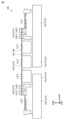
- the first portion 14c is electrically connected to the first input-side semiconductor module 1U11 via the first terminal 2a and the second terminal 2b.
- the first terminal 2a and the second terminal 2b are at different potentials.
- One of the first terminal 2a and the second terminal 2b is a positive potential side terminal, and the other of the first terminal 2a and second terminal 2b is a negative potential side terminal.
- Each of the first terminal 2a and the second terminal 2b is removably fixed to at least one of the first portion 14c of the printed circuit board 1U14 and the first input-side semiconductor module 1U11.
- each of the first terminal 2a and the second terminal 2b is non-removably fixed to the first portion 14c, and is removably fixed to the first input semiconductor module 1U11.
- the printed circuit board 1U14 is not directly fixed to the first semiconductor module 1U11, but is fixed to the first semiconductor module 1U11 via the first terminal 2a and the second terminal 2b. Thereby, an insulation distance between the first terminal 2a and the second terminal 2b can be ensured, and the contact resistance value with each terminal of the first semiconductor module 1U11 can be reduced or stabilized.
- the method of fixing each of the first terminal 2a and the second terminal 2b to the printed circuit board 1U14 or the first input-side semiconductor module 1U11 is not particularly limited.
- a via hole is formed in the first portion 14c, through which each of the first terminal 2a and the second terminal 2b is passed and fixed by caulking, soldering, or the like.
- the first input side semiconductor module 1U11 is formed with a terminal portion that contacts and is electrically connected to each of the first terminal 2a and the second terminal 2b, and a female screw portion into which a bolt is screwed. has been done. In the configuration shown in FIG.
- the printed circuit board 1U14, the first terminal 2a and the second terminal 2b, and the first input semiconductor module 1U11 can be fixed to each other.
- the printed circuit board 1U14 can be easily installed and replaced by attaching and detaching the bolts.
- the work of attaching and removing bolts is performed on one side of the power converter 100 in the second direction DR2 (for example, when the power converter 100 is applied to a control panel as described later, facing the front side of the control panel). Because it only needs to be done on the top surface, maintenance work becomes easier.
- each of the first terminal 2a and the second terminal 2b may be removably fixed to the first portion 14c and the first input-side semiconductor module 1U11, respectively.
- the first terminal 2a and the second terminal 2b are spaced apart from each other.
- the first terminal 2a and the second terminal 2b are spaced apart from each other in the first direction DR1, for example.
- a slit 14f is formed in the first portion 14c between the first terminal 2a and the second terminal 2b.
- the slit 14f is formed to cross an imaginary straight line connecting the first terminal 2a and the second terminal 2b at the shortest distance.
- the creepage distance between the first terminal 2a and the second terminal 2b is longer than the shortest distance (the length of a virtual straight line) between the first terminal 2a and the second terminal 2b. It's also long.
- the slit 14f has, for example, a longitudinal direction and a lateral direction.
- the longitudinal direction of the slit 14f is, for example, perpendicular to the virtual straight line.
- the second portion 14d is electrically connected to the first output side semiconductor module 1U12 via the third terminal 2c and the fourth terminal 2d.
- the third terminal 2c and the fourth terminal 2d may have the same configuration as the first terminal 2a and the second terminal 2b.
- the third terminal 2c and the fourth terminal 2d are at different potentials.
- One of the third terminal 2c and the fourth terminal 2d is a positive potential side terminal, and the other of the third terminal 2c and fourth terminal 2d is a negative potential side terminal.
- Each of the third terminal 2c and the fourth terminal 2d is removably fixed to at least one of the second portion 14d of the printed circuit board 1U14 and the first output side semiconductor module 1U12.
- each of the third terminal 2c and the fourth terminal 2d is non-removably fixed to the second portion 14d, and is removably fixed to the first output side semiconductor module 1U12.
- the method of fixing each of the third terminal 2c and the fourth terminal 2d to the printed circuit board 1U14 or the first output side semiconductor module 1U12 is also not particularly limited.
- the third terminal 2c and the fourth terminal 2d are spaced apart from each other.
- the third terminal 2c and the fourth terminal 2d are spaced apart from each other, for example, in the first direction DR1.
- a slit 14f is formed in the second portion 14d between the third terminal 2c and the fourth terminal 2d.
- the slit 14f is formed to cross an imaginary straight line connecting the third terminal 2c and the fourth terminal 2d at the shortest distance.
- the creepage distance between the third terminal 2c and the fourth terminal 2d is longer than the shortest distance (the length of a virtual straight line) between the third terminal 2c and the fourth terminal 2d. It's also long.
- the slit 14f has, for example, a longitudinal direction and a lateral direction.
- the longitudinal direction of the slit 14f is, for example, perpendicular to the virtual straight line.
- the first terminal 2a, the second terminal 2b, the third terminal 2c, and the fourth terminal 2d may be made of any conductive material, such as copper (Cu) or aluminum (Al).
- any conductive material such as copper (Cu) or aluminum (Al).
- Cu copper
- Al aluminum
- the external shape of each terminal is, for example, cylindrical, but is not limited to this, and may be a polygonal prism such as a square prism.
- first phase first capacitor 1U13 is mounted on the first surface 14a of the printed circuit board 1U14.
- other electronic components may be mounted on the first surface 14a in addition to the first phase first capacitor 1U13.
- at least one of a resistor and a capacitor used in a snubber circuit for suppressing surge voltage generated when the semiconductor module performs a switching operation may be further mounted on the first surface 14a.
- the printed circuit board 1U14 is, for example, a multilayer board including a plurality of conductor patterns stacked in the second direction DR2.
- the shape of each of the plurality of conductor patterns included in the printed circuit board 1U14 is not particularly limited.
- the cooler 1U15 includes the first cooling section 15a and the second cooling section 15b.
- the cooler 1U15 shown in FIG. 3 further includes a third cooling section 15c that connects the first cooling section 15a and the second cooling section 15b in the first direction DR1.
- the third cooling unit 15c is arranged at intervals from each of the plurality of first phase first capacitors 1U13 in the second direction DR2.
- Each of the plurality of first phase first capacitors 1U13 may be connected to the third cooling unit 15c of the cooler 1U15 via a spacer having high thermal conductivity.
- the first cooling unit 15a, the second cooling unit 15b, and the third cooling unit 15c constitute the cooler 1U15 as, for example, the same member.
- the cooler 1U15 may have any configuration as long as it can radiate the heat generated in the first phase unit group 1U.
- the cooler 1U15 may be a heat sink including, for example, a base portion and a plurality of fin portions.
- the plurality of fin parts may be arranged on the air blowing path of the cooling fan.
- the plurality of fin parts extend along the first direction DR1, and may be arranged at intervals in the third direction DR3.
- the cooling fan blows air in the first direction DR1.
- the cooler 1U15 may have an intake side wind tunnel and an exhaust side wind tunnel for concentrating the air flow generated by the cooling fan around the plurality of fins.
- the number and arrangement of cooling fans are not particularly limited.
- the cooling fan may be disposed on at least one of the intake side and the exhaust side of the cooler 1U15, and may be disposed on both sides, for example.
- a heat pipe may be embedded in the cooler 1U15.
- each of the first phase second power inverter circuit unit 1U2 and the first phase third power inverter circuit unit 1U3 has the same configuration as the first phase first power inverter circuit unit 1U1. is preferred.
- the first phase second power inverter circuit unit 1U2 includes a first phase second input semiconductor module 1U21, a first phase second output semiconductor module 1U22, and a first phase second capacitor 1U23 shown in FIG. Includes printed circuit board and cooler.
- the first phase third power inverter circuit unit 1U3 includes a first phase third input side semiconductor module 1U31, a first phase third output side semiconductor module 1U32, and a first phase third capacitor 1U33 shown in FIG. Includes printed circuit board and cooler.
- each of the first phase first power inverter circuit unit 1U1, the first phase second power inverter circuit unit 1U2, and the first phase third power inverter circuit unit 1U3 are adjacent to each other in the above described order in the third direction DR3. arranged to match.
- each of the second phase unit group 1V and the third phase unit group 1W have the same configuration as the first phase unit group 1U.
- the second phase unit group 1V includes a second phase first power inverter circuit unit, a second phase second power inverter circuit unit, and a second phase third power inverter circuit unit.
- the second phase first power inverter circuit unit, the second phase second power inverter circuit unit, and the second phase third power inverter circuit unit are arranged adjacent to each other in the above described order in the third direction DR3.
- the third phase unit group 1W includes a third phase first power inverter circuit unit, a third phase second power inverter circuit unit, and a third phase third power inverter circuit unit.
- the third phase first power inverter circuit unit, the third phase second power inverter circuit unit, and the third phase third power inverter circuit unit are arranged adjacent to each other in the above described order in the third direction DR3.
- each of the first phase unit group 1U, the second phase unit group 1V, and the third phase unit group 1W are arranged adjacent to each other in the above described order in the third direction DR3.
- the first phase first capacitor 1U13, the first phase second capacitor 1U23, and the first phase third capacitor 1U33 of the first phase unit group 1U are connected in parallel to each other.
- Capacitors (smoothing capacitors) included in each power inverter circuit unit of the first phase unit group 1U, the second phase unit group 1V, and the third phase unit group 1W are connected in parallel to each other. This keeps each capacitor at the same potential.
- each of the first phase first capacitor 1U13, first phase second capacitor 1U23, and first phase third capacitor 1U33 of the first phase unit group 1U may be mounted on the same printed circuit board 1U14. Furthermore, the capacitors (smoothing capacitors) included in each power conversion circuit unit of the first phase unit group 1U, second phase unit group 1V, and third phase unit group 1W are mounted on the same printed circuit board 1U14. Good too.
- Power conversion device 100 can be applied to an elevator control panel.
- the elevator control panel is installed in a machine room located above the hoistway through which the car moves, or within the hoistway.
- the power conversion device 100 converts power (for example, three-phase AC power) supplied from an external AC power source PW (for example, a commercial power source; hereinafter simply referred to as a power source) through an input reactor R1.
- the power is converted into power suitable for the upper machine M (for example, three-phase AC power).
- the converted power is supplied to the hoist M via the output reactor R2.
- three-phase AC power input from the power source PW to the power converter 100 via the input reactor R1 is divided into each of the first phase unit group 1U, second phase unit group 1V, and third phase unit group 1W. be done.
- the divided AC power is smoothed after being converted to DC power in each of the first phase unit group 1U, second phase unit group 1V, and third phase unit group 1W.
- the smoothed DC power is converted into AC power in each of the first phase unit group 1U, second phase unit group 1V, and third phase unit group 1W, and then merges to output reactor R2 as three-phase AC power. It is output to the hoisting machine M via.
- the input side semiconductor modules of each of the first phase unit group 1U, second phase unit group 1V, and third phase unit group 1W function as a converter that converts AC power to DC power.
- the output side semiconductor modules of each of the first phase unit group 1U, second phase unit group 1V, and third phase unit group 1W function as an inverter that converts DC power to AC power.
- Each capacitor in the first phase unit group 1U, second phase unit group 1V, and third phase unit group 1W functions as a smoothing capacitor.
- the power conversion device 100 converts regenerative power generated by the hoisting machine M into power suitable for charging the power source PW.
- the converted power is supplied to power supply PW.
- the other part including the output-side semiconductor module of each of the first phase unit group 1U, second phase unit group 1V, and third phase unit group 1W is a converter circuit that converts AC power into DC power.
- functions as The above-mentioned portion including the input-side semiconductor module of each of the first phase unit group 1U, second phase unit group 1V, and third phase unit group 1W functions as an inverter circuit that converts DC power to AC power.
- Power conversion device 100 returns regenerated power generated from hoist M to power source PW via input reactor R1.
- the power conversion device 100 can also be applied to uses other than elevator control panels.
- the power conversion device 100 can also be applied to, for example, a general-purpose inverter or an inverter for an air conditioner.
- the printed circuit board 1U14 on which the first phase first capacitor 1U13 is mounted is connected to the first phase first input side which is arranged to sandwich the first phase first capacitor 1U13 in the first direction DR1. Since it is supported by each of the semiconductor module 1U11 and the first phase first output side semiconductor module 1U12, the first phase first capacitor 1U13, the first phase first input side semiconductor module 1U11 and the first phase first output side semiconductor Connection failures are less likely to occur between each of the modules 1U12.
- the power conversion device 100 In the power conversion device 100, poor connection between the first phase first capacitor 1U13 and other electronic components is less likely to occur, compared to a power conversion device in which the board on which the capacitor is mounted is supported in a cantilevered state by a connector. . In particular, even if vibrations are applied to the printed circuit board 1U14 during use or transportation of the power conversion device 100, the power conversion device 100 is configured to connect the first phase first capacitor 1U13, the first phase first input side semiconductor module 1U11, and the first phase first input side semiconductor module 1U11. Connection failures are less likely to occur between each of the 1-phase first output side semiconductor modules 1U12.
- the printed circuit board 1U14 on which the first phase first capacitor 1U13, which is a smoothing capacitor, is mounted is used for the first phase first input side semiconductor module 1U11 and the first phase first output side semiconductor module 1U12. Each is detachably supported. Therefore, in the power conversion device 100, the smoothing capacitor can be replaced more easily than in a power conversion device in which the smoothing capacitor is mounted on the same substrate as the semiconductor element.
- the smoothing capacitor is an electrolytic capacitor, its lifespan is about 10 to 15 years. If the power converter 100 is used for a longer period than the life of the smoothing capacitor, the smoothing capacitor must be replaced. Even in such a case, according to the power conversion device 100, the smoothing capacitor can be replaced only by attaching and detaching the printed circuit board 1U14.
- the first phase first input semiconductor module 1U11 and the first phase first output semiconductor module 1U12 are removably supported by the cooler 1U15.
- the first phase first input side semiconductor module 1U11, the first phase first output side semiconductor module 1U12, and the printed circuit board 1U14 can be easily changed. Can be exchanged.
- each of the first phase first input side semiconductor module 1U11 and the first phase first output side semiconductor module 1U12 is arranged so as to sandwich the first phase first capacitor 1U13 in the first direction DR1.
- the length (thickness) of the power conversion device 100 in the second direction DR2 is such that each of the first phase first input side semiconductor module 1U11 and the first phase first output side semiconductor module 1U12 has a length (thickness) in the second direction DR1. It is shorter (thinner) than when it is not arranged to sandwich the 1-phase first capacitor 1U13.
- the first cooling unit 15a and the second cooling unit 15b are arranged on the first phase first capacitor 1U13 side with respect to the printed circuit board 1U14 in the second direction DR2, and 1U13 is arranged with an interval between the first cooling section 15a and the second cooling section 15b. Therefore, the first phase first capacitor 1U13 is not easily affected by vibrations of the first cooling section 15a and the second cooling section 15b.
- the first phase first capacitor 1U13 when the first phase first capacitor 1U13 is not in contact with other electronic components, the first phase first capacitor 1U13 is less susceptible to vibrations of the electronic component, and Heat input to the 1-phase first capacitor 1U13 is suppressed.
- first phase first capacitors 1U13 are mounted on the printed circuit board 1U14.
- the number of first phase first capacitors 1U13 mounted on printed circuit board 1U14 can be arbitrarily set depending on the capacity required of power converter 100.
- the creepage distance between the first terminal 2a and the second terminal 2b is The distance between the first terminal 2a and the second terminal 2b becomes longer than the shortest distance (the length of a virtual straight line).
- the creepage distance between the first terminal 2a and the second terminal 2b is set to be greater than or equal to the distance required to electrically insulate the first terminal 2a and the second terminal 2b.
- the power conversion device 100 may be provided to configure the power conversion circuit shown in FIG. 5 instead of the power conversion circuit shown in FIG. 1.
- the power conversion device 100 shown in FIG. 5 includes each of a first phase unit 10U, a second phase unit 10V, and a third phase unit 10W.
- Each of the first phase unit 10U, second phase unit 10V, and third phase unit 10W constitutes one power inverter circuit unit for one phase and three parallel units.
- the power conversion device 100 shown in FIG. 5 is the power conversion device shown in FIG. 1 in that each of the first phase unit 10U, second phase unit 10V, and third phase unit 10W includes only one smoothing capacitor It is different from 100.
- a first phase unit 10U as one power conversion circuit unit includes a first phase input side semiconductor module 1U16 as an input side semiconductor module, and a first phase input side semiconductor module 1U16 as an output side semiconductor module. It has a phase output side semiconductor module 1U17 and a first phase capacitor 1U18.
- the relative positional relationship and connection relationship of the first phase input side semiconductor module 1U16, the first phase output side semiconductor module 1U17, and the first phase capacitor 1U18 are the same as those shown in FIGS. It suffices if it is equivalent to each of the phase first input side semiconductor module 1U11, the first phase first output side semiconductor module 1U12, and the first phase first capacitor 1U13.
- the cooler 1U15 of the power conversion device 100 may include two coolers: a first cooling section 15a and a second cooling section 15b.
- the first cooling unit 15a has an interval between the first cooling unit 15a and each of the plurality of first phase first capacitors 1U13 arranged near the first phase first input side semiconductor module 1U11 in the first direction DR1. It may also be configured with a fourth cooling section 15c1 spaced apart from each other.
- the second cooling unit 15b is spaced apart from the second cooling unit 15b and each of the plurality of first phase first capacitors 1U13 arranged near the first phase first output side semiconductor module 1U12 in the first direction DR1.
- the fifth cooling unit 15c2 may be arranged with a space between the cooling units 15c2 and 15c2. That is, the first cooling section 15a and the second cooling section 15b may be separate members from each other.
- the heat capacity of each of the first cooling section 15a and the second cooling section 15b is arbitrarily set according to the amount of heat generated by each of the first phase first input side semiconductor module 1U11 and the first phase first output side semiconductor module 1U12. obtain.
- the calorific value of the first phase first input side semiconductor module 1U11 is greater than the calorific value of the first phase first output side semiconductor module 1U12, as shown in FIG. It is preferable that the heat capacity is larger than that of the second cooling part 15b.
- the cooler 1U15 shown in FIG. 6 has improved workability (portability and installability) compared to the cooler 1U15 shown in FIG. 3. Moreover, in the cooler 1U15 shown in FIG. 6, an inexpensive cooler can be used as the second cooling part 15b having a relatively small heat capacity.
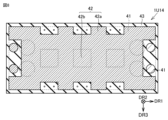
- the power conversion device according to the second embodiment has basically the same configuration as the power conversion device 100 according to the first embodiment and has the same effects, but as shown in FIGS. 7 and 8, the power conversion device 100 has a printed circuit board 1U14 further includes a first conductor pattern 41 and a second conductor pattern 42 having different potentials, and the area of the region of the second conductor pattern 42 facing the first conductor pattern 41 in the second direction DR2 is a second conductor pattern.
- the differences between the power conversion device according to the second embodiment and the power conversion device 100 according to the first embodiment will be mainly explained. Note that in FIG. 7, the outer edge of the second conductor pattern 42 shown in FIG. 8 is shown by a broken line. In FIG. 8, the outer edge of the first conductor pattern 41 shown in FIG. 7 is shown by a broken line.
- the first conductor pattern 41 and the second conductor pattern 42 are spaced apart from each other in the second direction DR2.
- Each of the first conductor pattern 41 and the second conductor pattern 42 is covered with an insulating film 43 and electrically insulated from each other by the insulating film 43.
- the first conductor pattern 41 is electrically connected to the first terminal 2a via a via hole (not shown) or the like. That is, the first conductor pattern 41 is electrically connected to the first phase first input side semiconductor module 1U11 via the first terminal 2a and the like. Further, the first conductor pattern 41 is electrically connected to one electrode of the first phase first capacitor 1U13 via a via hole or the like (not shown).
- the second conductor pattern 42 is electrically connected to the second terminal 2b via a via hole (not shown) or the like. That is, the second conductor pattern 42 is electrically connected to the first phase first output side semiconductor module 1U12 via the second terminal 2b and the like. Furthermore, the second conductor pattern 42 is electrically connected to the other electrode of the first phase first capacitor 1U13 via a via hole (not shown) or the like.
- the area of the region of the first conductor pattern 41 that faces the second conductor pattern 42 in the second direction DR2 is 20% or more of the area of the first conductor pattern 41.
- the area of the region of the second conductor pattern 42 that faces the first conductor pattern 41 in the second direction DR2 is 20% or more of the area of the second conductor pattern 42.
- the area of the region of the second conductor pattern 42 facing the first conductor pattern 41 in the second direction DR2 is less than 20% of the area of the second conductor pattern 42;
- the capacitance formed by the first conductor pattern 41 and the second conductor pattern 42 increases, and the parasitic inductance component is reduced.
- the shapes of each of the first conductor pattern 41 and the second conductor pattern 42 are not limited to the shapes shown in FIGS. 7 and 8, and may be arbitrarily set. can be done.
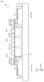
- Power converter 101 according to Embodiment 3 has basically the same configuration as power converter 100 according to Embodiment 1, and has similar effects, but as shown in FIG. 1 capacitor 1U13 in the second direction DR2 is longer than the length L1 in the second direction DR2 of each of the first phase first input side semiconductor module 1U11 and the first phase first output side semiconductor module 1U12. This differs from the power conversion device 100 in that a part of the one-phase first capacitor 1U13 is disposed between the first cooling section 15a and the second cooling section 15b in the first direction DR1. Below, the differences between the power conversion device 101 and the power conversion device 100 will be mainly explained.
- the area of each of the two electrodes of one first phase first capacitor 1U13 can be set larger than that of the power conversion device 100 according to the first embodiment.
- the capacitance of the two first phase first capacitors 1U13 can be set large.
- the first phase 1 Since the number of capacitors 1U13 can be reduced, the area of the third portion 14e on which the first phase first capacitor 1U13 is mounted on the printed circuit board 1U14 can be reduced in size.
- the first cooling section 15a and the second cooling section 15b may be separate members.
- the cooler 1U15 may include a first cooling section 15a and a second cooling section 15b that are separated from each other.
- the first phase first capacitor 1U13 will not come into contact with the cooler 1U15 and will be spaced apart from the cooler 1U15. It can be arranged as follows.
- the first cooling section 15a and the second cooling section 15b can be cooled as the same member. It may constitute the container 1U15.
- the thickness in the second direction DR2 of the portion of the cooler 1U15 that faces the first phase first capacitor 1U13 in the second direction DR2 is the same as the thickness in the second direction DR2 of each of the first cooling section 15a and the second cooling section 15b. It may be thinner than the thickness.
- the power conversion device 102 according to the fourth embodiment has basically the same configuration as the power conversion device 100 according to the first embodiment and has the same effects, but the power conversion device 102 according to the fourth embodiment It differs from power converter 100 in that it further includes at least one capacitor 1U19 mounted on second surface 14b. Below, the differences between the power conversion device 102 and the power conversion device 100 will be mainly explained.
- the power conversion device 102 includes, for example, a plurality of capacitors 1U19.
- Each of the plurality of capacitors 1U19 is mounted on the third portion 14e of the printed circuit board 1U14.
- Each of the plurality of capacitors 1U19 is connected in parallel with, for example, the first phase first capacitor 1U13.
- the first phase first output side semiconductor module 1U12 is electrically connected to the first phase first input side semiconductor module 1U11 via a plurality of first phase first capacitors 1U13 and a plurality of capacitors 1U19.
- the power conversion device 102 when the combined capacitance of the plurality of first phase first capacitors 1U13 and the plurality of capacitors 1U19 is equal to the combined capacitance of the plurality of first phase first capacitors 1U13 of the power conversion device 100, the power Since the number of first phase first capacitors 1U13 required to realize the capacitance can be reduced compared to the converter 100, the first phase first capacitor 1U13 and capacitor 1U19 are mounted on the printed circuit board 1U14. The area of the third portion 14e can be reduced.
- the length L3 in the second direction DR2 of each of the plurality of capacitors 1U19 is shorter than the length L2 in the second direction DR2 of each of the plurality of first phase first capacitors 1U13.
- the length (thickness) in the second direction DR2 of the power conversion device 102 is the same as the length (thickness) in the second direction DR2 of each of the plurality of capacitors 1U19. It becomes shorter (thinner) than the case where it is longer than the length in the second direction DR2.
- the length L3 of each of the plurality of capacitors 1U19 in the second direction DR2 is shorter than the length L1 of the first phase first input side semiconductor module 1U11 in the second direction DR2.
- Each of the plurality of first phase first capacitors 1U13 and the plurality of capacitors 1U19 may be a lead-type capacitor or a surface-mounted capacitor.
- each of the plurality of capacitors 1U19 is a surface mount type capacitor.
- the mounting density of the plurality of capacitors 1U19 can be increased.
- the lead of the capacitor that is mounted later on one surface is mounted first on the other surface. In this case, it is difficult to fix the leads of the capacitor to be mounted later on the other surface with solder.
- each of the plurality of capacitors 1U19 is a surface mount type capacitor, the plurality of capacitors 1U19 are not arranged on the first surface 14a, so the above problem is less likely to occur.
- each of the first phase first capacitor 1U13 and the plurality of capacitors 1U19 may be a lead type capacitor.
- power conversion device 103 according to Embodiment 5 has basically the same configuration as power conversion device 100 according to Embodiment 1, and has similar effects, but It differs from the power conversion device 100 in that it further includes at least one support member 51a fixed to the center of the substrate 1U14 in the long side direction (first direction DR1). Below, the differences between power conversion device 103 and power conversion device 100 will be mainly explained.
- the power conversion device 103 includes a plurality of support members 51a and 51b arranged between the printed circuit board 1U14 and the cooler 1U15.
- Each of the plurality of supporting members 51a, 51b does not electrically connect between the printed circuit board 1U14 and the cooler 1U15, but rather changes the relative position of the printed circuit board 1U14 with respect to the cooler 1U15 in the second direction DR2. This is to suppress the From a different perspective, each of the plurality of support members 51a, 51b is for increasing the strength of fixing the printed circuit board 1U14 to the cooler 1U15.
- Each of the plurality of support members 51a and 51b extends along the second direction DR2.
- the length of each of the plurality of support members 51a, 51b in the second direction DR2 is longer than the length of each of the plurality of capacitors 1U13 in the second direction DR2. That is, each of the plurality of support members 51a, 51b can maintain a state in which each capacitor 1U13 is not in contact with the cooler 1U15.
- each of the plurality of support members 51a, 51b in the second direction DR2 is fixed, for example, to the center of the printed circuit board 1U14 in the long side direction (first direction DR1). From a different perspective, one end of each of the plurality of support members 51a, 51b in the second direction DR2 is fixed to a central portion between the first terminal 2a and the third terminal 2c in the first direction DR1. One end of each of the plurality of support members 51a, 51b in the second direction DR2 is fixed, for example, to both ends of the printed circuit board 1U14 in the short side direction (third direction DR3). From a different perspective, each of the plurality of supporting members 51a and 51b is arranged so as to sandwich the plurality of capacitors 1U13 in each of the first direction DR1 and the third direction DR3.
- each of the plurality of support members 51a, 51b in the second direction DR2 is fixed to, for example, the cooler 1U15.
- the other end of each of the plurality of support members 51a, 51b in the second direction DR2 is spaced apart from each of the plurality of first phase first capacitors 1U13 in the second direction DR2 of the cooler 1U15, for example.
- the third cooling part 15c is fixed to the third cooling part 15c.
- each of the plurality of support members 51a, 51b in the second direction DR2 only needs to be in contact with the cooler 1U15, and does not need to be fixed to the cooler 1U15.
- the other end of each of the plurality of support members 51a, 51b in the second direction DR2 should just be in contact with the third cooling part 15c.
- the number of supporting members may be any number greater than or equal to one.
- one support member may be disposed at the center in the first direction DR1 and only on one side with respect to the capacitor 1U13 in the third direction DR3.
- the natural vibration frequency at which the printed circuit board 1U14 vibrates when vibration is applied to the power conversion device 103 is determined by the support member 51a. This results in a shift to a higher frequency side than the state before 51a is placed.
- the amount of deformation of the printed circuit board 1U14 is reduced compared to the power conversion device 100 that does not include at least one support member 51a, so the printed circuit board 1U14 is less likely to be damaged. It is expected that the life of the substrate 1U14 will be extended.
- the deformation of the printed circuit board 1U14 is further reduced compared to the power conversion device 103 that includes only one support member 51a. Can be suppressed.
- the power conversion device 103 may include three or more support members arranged at intervals in at least one of the first direction DR1 and the third direction DR3.
- the shape of the support member 51a is, for example, cylindrical, but is not limited to this.
- the shape of the support member 51a may be, for example, a polygonal prism such as a square prism or a hexagonal prism.
- the support member 51a may be provided as a terminal block that can be mounted on the printed circuit board 1U14.
- any method may be used to fix the one end of the support member 51a in the second direction DR2 to the printed circuit board 1U14, such as fastening with screws, caulking, or soldering.
- the fixing method may be any arbitrary method, such as fastening with screws, caulking, or soldering. .
- the support member 51a may be composed of one member, or may be composed of a plurality of members.
- the material constituting the support member 51a may be any material as long as it can suppress fluctuations in the relative position of the printed circuit board 1U14 with respect to the cooler 1U15 in the second direction DR2, and examples thereof include stainless steel, brass, and aluminum. and resin materials such as nylon and polyphenylene sulfide (PPS).
- PPS polyphenylene sulfide
- the power conversion device 103 is the same as that of the second or fourth embodiment, except that it further includes at least one support member 51a fixed to the central portion of the printed circuit board 1U14 in the long side direction (first direction DR1). It may have the same configuration as the power conversion device. For example, in the power conversion device 103, at least one support member 51a may be in contact with the fourth cooling section 15c1 or the fifth cooling section 15c2 shown in FIG. 6.
- a printed circuit board having a first surface; at least one capacitor mounted on the first surface of the printed circuit board; an input-side semiconductor module and an output-side semiconductor that are arranged to sandwich the at least one capacitor in a first direction along the first surface and are electrically connected to each other via the at least one capacitor; Equipped with a module, A power conversion device, wherein the printed circuit board is removably supported by each of the input-side semiconductor module and the output-side semiconductor module.
- the first cooling unit and the second cooling unit constitute a cooler as mutually identical members, The power conversion device according to [Additional Note 2], wherein the cooler has a portion spaced apart from the at least one capacitor in the second direction.
- the printed circuit board further includes a first terminal and a second terminal that are electrically connected to the input-side semiconductor module and have different potentials from each other,
- the power conversion device according to any one of [Appendix 1] to [Appendix 6], wherein a slit is formed in the printed circuit board between the first terminal and the second terminal.
- the printed circuit board further includes a first conductor pattern and a second conductor pattern that are spaced apart from each other in a second direction perpendicular to the first surface and have different potentials from each other, Any of [Appendix 1] to [Appendix 7], wherein the area of the region of the second conductor pattern that faces the first conductor pattern in the second direction is 20% or more of the area of the second conductor pattern.
- the power conversion device according to claim 1.
- the at least one capacitor is a plurality of capacitors; Any one of [Appendix 1] to [Appendix 8], wherein each of the plurality of capacitors has a portion that overlaps each of the input-side semiconductor module and the output-side semiconductor module when viewed from the first direction.
- the printed circuit board further has a second surface located opposite to the first surface, The power conversion device according to any one of [Appendix 1] to [Appendix 9], further comprising at least one capacitor mounted on the second surface of the printed circuit board.
- the printed circuit board has at least one support member located on the first surface, The power conversion device according to any one of [Appendix 1] to [Appendix 10], wherein the support member is in contact with the cooling section.
- 1U 1st phase unit group 1U1 1st phase 1st power inverter circuit unit, 1U2 1st phase 2nd power inverter circuit unit, 1U3 1st phase 3rd power inverter circuit unit, 1U11 1st phase 1st input side semiconductor module , 1U12 1st phase 1st output side semiconductor module, 1U13 1st phase 1st phase 1st capacitor, 1U14 Printed circuit board, 1U15 Cooler, 1U21 1st phase 2nd input side semiconductor module, 1U22 1st phase 2nd output side Semiconductor module, 1U23 1st phase 2nd capacitor, 1U31 1st phase 3rd input side semiconductor module, 1U32 1st phase 3rd output side semiconductor module, 1U33 1st phase 3rd capacitor, 1U16 1st phase input side semiconductor module, 1U17 1st phase output side semiconductor module, 1U18, 1U19 capacitor, 1V 2nd phase unit group, 1W 3rd phase unit group, 2
Landscapes
- Engineering & Computer Science (AREA)
- Microelectronics & Electronic Packaging (AREA)
- Physics & Mathematics (AREA)
- Thermal Sciences (AREA)
- Power Engineering (AREA)
- Inverter Devices (AREA)
Priority Applications (3)
| Application Number | Priority Date | Filing Date | Title |
|---|---|---|---|
| JP2024543831A JP7728980B2 (ja) | 2022-09-02 | 2023-07-04 | 電力変換装置 |
| CN202380061454.7A CN119769012A (zh) | 2022-09-02 | 2023-07-04 | 电力转换装置 |
| US18/992,235 US20260032846A1 (en) | 2022-09-02 | 2023-07-04 | Power conversion device |
Applications Claiming Priority (2)
| Application Number | Priority Date | Filing Date | Title |
|---|---|---|---|
| JP2022140139 | 2022-09-02 | ||
| JP2022-140139 | 2022-09-02 |
Publications (1)
| Publication Number | Publication Date |
|---|---|
| WO2024048066A1 true WO2024048066A1 (ja) | 2024-03-07 |
Family
ID=90099461
Family Applications (1)
| Application Number | Title | Priority Date | Filing Date |
|---|---|---|---|
| PCT/JP2023/024793 Ceased WO2024048066A1 (ja) | 2022-09-02 | 2023-07-04 | 電力変換装置 |
Country Status (4)
| Country | Link |
|---|---|
| US (1) | US20260032846A1 (https=) |
| JP (1) | JP7728980B2 (https=) |
| CN (1) | CN119769012A (https=) |
| WO (1) | WO2024048066A1 (https=) |
Citations (3)
| Publication number | Priority date | Publication date | Assignee | Title |
|---|---|---|---|---|
| JP2000060134A (ja) * | 1998-08-05 | 2000-02-25 | Hitachi Ltd | インバータ装置 |
| JP2015073376A (ja) * | 2013-10-03 | 2015-04-16 | 三菱電機株式会社 | 電力変換装置 |
| JP2015186275A (ja) * | 2014-03-20 | 2015-10-22 | 住友電気工業株式会社 | 変換装置 |
Family Cites Families (10)
| Publication number | Priority date | Publication date | Assignee | Title |
|---|---|---|---|---|
| JPS5656683U (https=) * | 1979-10-08 | 1981-05-16 | ||
| JP2809026B2 (ja) * | 1992-09-30 | 1998-10-08 | 三菱電機株式会社 | インバ−タ装置およびインバ−タ装置の使用方法 |
| JPH07245951A (ja) * | 1994-03-07 | 1995-09-19 | Toshiba Corp | 半導体スタック |
| JP3749170B2 (ja) * | 2001-12-27 | 2006-02-22 | 三洋電機株式会社 | 電源装置 |
| JP4929299B2 (ja) * | 2009-02-17 | 2012-05-09 | 株式会社日立製作所 | 電力変換装置 |
| CN102326326B (zh) * | 2009-02-24 | 2014-03-26 | 东芝三菱电机产业系统株式会社 | 半导体堆叠体及利用半导体堆叠体的功率转换装置 |
| JP2012165611A (ja) * | 2011-02-09 | 2012-08-30 | Mitsubishi Electric Corp | 半導体ユニット及び電力変換装置 |
| JP5796257B2 (ja) * | 2012-05-31 | 2015-10-21 | アイシン・エィ・ダブリュ株式会社 | インバータ装置 |
| JP6457381B2 (ja) * | 2015-12-21 | 2019-01-23 | 株式会社日立製作所 | 電力変換装置およびエレベータ |
| JP6811762B2 (ja) * | 2018-12-18 | 2021-01-13 | 日立ジョンソンコントロールズ空調株式会社 | 電力変換装置、及び、これを備える冷凍サイクル装置 |
-
2023
- 2023-07-04 JP JP2024543831A patent/JP7728980B2/ja active Active
- 2023-07-04 WO PCT/JP2023/024793 patent/WO2024048066A1/ja not_active Ceased
- 2023-07-04 CN CN202380061454.7A patent/CN119769012A/zh active Pending
- 2023-07-04 US US18/992,235 patent/US20260032846A1/en active Pending
Patent Citations (3)
| Publication number | Priority date | Publication date | Assignee | Title |
|---|---|---|---|---|
| JP2000060134A (ja) * | 1998-08-05 | 2000-02-25 | Hitachi Ltd | インバータ装置 |
| JP2015073376A (ja) * | 2013-10-03 | 2015-04-16 | 三菱電機株式会社 | 電力変換装置 |
| JP2015186275A (ja) * | 2014-03-20 | 2015-10-22 | 住友電気工業株式会社 | 変換装置 |
Also Published As
| Publication number | Publication date |
|---|---|
| JP7728980B2 (ja) | 2025-08-25 |
| US20260032846A1 (en) | 2026-01-29 |
| JPWO2024048066A1 (https=) | 2024-03-07 |
| CN119769012A (zh) | 2025-04-04 |
Similar Documents
| Publication | Publication Date | Title |
|---|---|---|
| JP3501685B2 (ja) | 電力変換装置 | |
| US20110221268A1 (en) | Power Converter and In-Car Electrical System | |
| US8547698B2 (en) | Cooling structure of capacitor and inverter device | |
| CN108417542B (zh) | 一种电机控制器功率单元总成 | |
| JP7303087B2 (ja) | 平滑コンデンサ部及びスナバコンデンサを有するモータ駆動装置 | |
| CN109412431B (zh) | 叠层铜排及三相大功率逆变器 | |
| JP2015100223A (ja) | 電力変換装置 | |
| JP2009027778A (ja) | バスバー | |
| US7902464B2 (en) | Heat sink arrangement for electrical apparatus | |
| CN111244047B (zh) | 一种基于GaN器件的双面散热全桥功率模块 | |
| CN218868114U (zh) | 驱动模组以及控制柜 | |
| JP6102668B2 (ja) | 電力変換装置 | |
| US20090195066A1 (en) | Power converter | |
| JP2006197735A (ja) | インバータ装置 | |
| JP2008263755A (ja) | スイッチング電源装置 | |
| WO2024048066A1 (ja) | 電力変換装置 | |
| CN209472561U (zh) | 叠层铜排及三相大功率逆变器 | |
| JP7570528B2 (ja) | 電力変換装置 | |
| JP7006464B2 (ja) | 電力変換装置 | |
| JP2019062739A (ja) | 電力変換装置 | |
| JP2007159254A (ja) | 電力変換装置 | |
| WO2023115985A1 (zh) | 一种新型的汽车逆变器用高压陶瓷母线支撑电容 | |
| JP2024003915A (ja) | 電力変換器 | |
| JP2005191233A (ja) | パワーモジュール | |
| WO2023037523A1 (ja) | 電力変換装置 |
Legal Events
| Date | Code | Title | Description |
|---|---|---|---|
| 121 | Ep: the epo has been informed by wipo that ep was designated in this application |
Ref document number: 23859836 Country of ref document: EP Kind code of ref document: A1 |
|
| ENP | Entry into the national phase |
Ref document number: 2024543831 Country of ref document: JP Kind code of ref document: A |
|
| WWE | Wipo information: entry into national phase |
Ref document number: 18992235 Country of ref document: US |
|
| WWE | Wipo information: entry into national phase |
Ref document number: 202380061454.7 Country of ref document: CN |
|
| NENP | Non-entry into the national phase |
Ref country code: DE |
|
| WWP | Wipo information: published in national office |
Ref document number: 202380061454.7 Country of ref document: CN |
|
| 122 | Ep: pct application non-entry in european phase |
Ref document number: 23859836 Country of ref document: EP Kind code of ref document: A1 |
|
| WWP | Wipo information: published in national office |
Ref document number: 18992235 Country of ref document: US |