WO2024047733A1 - 光伝送システム及び信号歪み補償方法 - Google Patents
光伝送システム及び信号歪み補償方法 Download PDFInfo
- Publication number
- WO2024047733A1 WO2024047733A1 PCT/JP2022/032540 JP2022032540W WO2024047733A1 WO 2024047733 A1 WO2024047733 A1 WO 2024047733A1 JP 2022032540 W JP2022032540 W JP 2022032540W WO 2024047733 A1 WO2024047733 A1 WO 2024047733A1
- Authority
- WO
- WIPO (PCT)
- Prior art keywords
- signal
- optical
- nonlinear
- signal distortion
- operation mode
- Prior art date
- Legal status (The legal status is an assumption and is not a legal conclusion. Google has not performed a legal analysis and makes no representation as to the accuracy of the status listed.)
- Ceased
Links
Images





Classifications
-
- H—ELECTRICITY
- H04—ELECTRIC COMMUNICATION TECHNIQUE
- H04B—TRANSMISSION
- H04B10/00—Transmission systems employing electromagnetic waves other than radio-waves, e.g. infrared, visible or ultraviolet light, or employing corpuscular radiation, e.g. quantum communication
- H04B10/50—Transmitters
- H04B10/58—Compensation for non-linear transmitter output
-
- H—ELECTRICITY
- H04—ELECTRIC COMMUNICATION TECHNIQUE
- H04B—TRANSMISSION
- H04B10/00—Transmission systems employing electromagnetic waves other than radio-waves, e.g. infrared, visible or ultraviolet light, or employing corpuscular radiation, e.g. quantum communication
- H04B10/60—Receivers
- H04B10/61—Coherent receivers
Definitions
- the present invention relates to an optical transmission system and a signal distortion compensation method.
- Nonlinear distortion caused by semiconductor optical amplifiers can be reduced by increasing the symbol rate of the signal.
- an SNR (Signal to Noise Ratio) penalty of about 1 dB occurs.
- highly accurate compensation techniques are required in signal processing even for high symbol rate signals.
- a gain coefficient of distortion caused by the semiconductor optical amplifier is calculated based on the physical parameters of the semiconductor optical amplifier estimated using the received signal, and an inverse characteristic of the calculated gain coefficient is applied to the signal.
- Nonlinear signal distortion is compensated for by multiplication.
- the accuracy of estimating the physical parameters of the semiconductor optical amplifier deteriorates. Therefore, there is a problem in that the accuracy of compensating for nonlinear distortion caused by the semiconductor optical amplifier deteriorates.
- the present invention aims to provide a technique that can improve the accuracy of compensating for nonlinear distortion caused by a semiconductor optical amplifier.
- One aspect of the present invention is an optical transmission system including an optical transmitter and an optical receiver, wherein the optical transmitter has a first operation mode that generates a low symbol rate signal and a high symbol rate signal. an operation mode control unit that sets one of the second operation modes that generates a second operation mode, and a transmission signal generation unit that generates a transmission signal according to the operation mode set by the operation mode control unit,
- the optical receiver includes an optical coherent receiver that acquires an optical signal based on the transmitted signal and generates a received signal based on the optical signal, and a digital signal processing unit that performs digital signal processing on the received signal.
- a reception data demodulation unit that demodulates binary information of a transmission data series based on the reception signal subjected to the digital signal processing, and the optical transmitter or the optical receiver transmits data using a semiconductor optical amplifier.
- a nonlinear signal distortion compensation unit that calculates a gain coefficient of nonlinear signal distortion occurring in a signal based on an estimated value of a physical parameter of the semiconductor optical amplifier, and multiplies the transmission signal by a value representing an inverse characteristic of the gain coefficient; a nonlinear signal distortion estimation unit that acquires a transmission signal and estimates the nonlinear signal distortion based on a comparison result of the transmission signal and the reception signal; and a nonlinear signal distortion estimation unit that estimates the nonlinear signal distortion based on the nonlinear signal distortion estimated by the nonlinear signal distortion estimation unit.
- the optical receiver is configured to perform the digital signal processing when the optical transmitter is operating in a first operation mode.
- the output destination is switched such that the received signal subjected to the digital signal processing is output to the nonlinear signal distortion estimator, and the optical transmitter is operating in the second operation mode, the received signal subjected to the digital signal processing is
- This is an optical transmission system that switches an output destination so that the received data is output to the demodulator.
- One aspect of the present invention is a signal distortion compensation method performed by an optical transmission system including an optical transmitter and an optical receiver, wherein the optical transmitter operates in a first operation mode in which a low symbol rate signal is generated. , a second operation mode that generates a high symbol rate signal, the optical transmitter generates a transmission signal according to the set operation mode, and the optical receiver an optical signal based on a transmission signal is obtained, a reception signal is generated based on the optical signal, the optical receiver performs digital signal processing on the reception signal, and the optical receiver performs digital signal processing on the reception signal.
- the optical transmitter or the optical receiver Based on the received signal, the optical transmitter or the optical receiver demodulates the binary information of the transmitted data sequence, and the optical transmitter or the optical receiver calculates the gain coefficient of the nonlinear signal distortion caused in the transmitted signal by the semiconductor optical amplifier. Calculated based on estimated values of physical parameters of the amplifier, multiplies the transmitted signal by a value representing the inverse characteristic of the gain coefficient, obtains the transmitted signal, and calculates the transmitted signal based on the comparison result of the transmitted signal and the received signal. , estimating the nonlinear signal distortion and estimating physical parameters of the semiconductor optical amplifier based on the estimated nonlinear signal distortion, and the optical receiver and the optical transmitter are operating in a first operation mode.
- the output destination is switched so that the received signal subjected to the digital signal processing is output to a nonlinear signal distortion estimator that estimates the nonlinear signal distortion, and the optical transmitter operates in a second operation mode.
- the output destination is switched so that the received signal subjected to the digital signal processing is output to a received data demodulation section that demodulates the binary information of the transmitted data series.
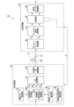
- FIG. 2 is a diagram showing an example of the configuration of an optical transceiver in the first embodiment.
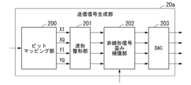
- FIG. 3 is a diagram illustrating a configuration example of a transmission signal generation section in the first embodiment.
- FIG. 2 is a sequence diagram showing the flow of processing of the optical transmission system in the first embodiment.
- FIG. 2 is a sequence diagram showing the flow of processing of the optical transmission system in the first embodiment. It is a figure showing an example of composition of an optical transceiver in a 2nd embodiment. It is a figure showing an example of composition of an optical transceiver in a 3rd embodiment. It is a figure showing the example of composition of the optical transceiver in a 4th embodiment.
- FIG. 1 is a diagram showing an example of the configuration of an optical transceiver in the first embodiment.
- FIG. 3 is a diagram illustrating a configuration example of a transmission signal generation section in the first embodiment.
- FIG. 2 is a sequence diagram showing the flow of processing of the optical transmission system in the first embodiment.
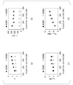
- FIG. 3 is a diagram showing the relationship between injection current, physical parameters, and line width increase coefficient ⁇ . It is a figure for explaining the effect in a 4th embodiment.
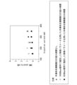
- FIG. 3 is a diagram showing a constellation when the injection current of the semiconductor optical amplifier is 350 mA in a high symbol rate signal of 168 GBaud. It is a figure showing the example of composition of the optical transceiver in a 5th embodiment.
- FIG. 1 is a diagram showing a configuration example of an optical transceiver 1a in the first embodiment.
- the optical transceiver 1a (optical transmission system) is a communication device that uses optical signals.
- the optical transceiver 1a includes an optical transmitter 2a, a transmission line 3, an optical receiver 4a, and a control channel 5.
- the optical transmitter 2a is a communication device that transmits optical signals.
- the optical transmitter 2a operates in multiple operation modes. For example, the optical transmitter 2a operates by switching between a first operation mode and a second operation mode.
- the first operation mode is an operation mode used when estimating physical parameters of a semiconductor optical amplifier.
- the optical transmitter 2a generates a low symbol rate signal when operating in the first mode of operation.
- the second operation mode is an operation mode used after estimating the physical parameters of the semiconductor optical amplifier.
- the optical transmitter 2a generates a high symbol rate signal when operating in the second mode of operation.
- the low symbol rate signal is a 42 GB aud signal
- the high symbol rate signal is a 168 GB aud signal. Note that the low symbol rate signal and the high symbol rate signal are not limited to the above example.
- the optical receiver 4a may include a semiconductor optical amplifier 22.
- the transmission line 3 may include a semiconductor optical amplifier 22.
- the optical transmitter 2a includes an operation mode control section 10, a transmission signal generation section 20a, an optical modulator 21, and a semiconductor optical amplifier 22. Note that the optical transmitter 2a includes a semiconductor optical amplifier 22 either built-in or externally attached.
- the operation mode control unit 10 controls the operation mode of the optical transmitter 2a. Specifically, the operation mode control unit 10 sets the optical transmitter 2a to operate in the first operation mode or the second operation mode as the operation mode of the optical transmitter 2a.
- the transmission signal generation unit 20a generates a modulated signal sequence (XI, XQ, YI, YQ) based on a transmission data sequence that is binary information.
- the transmission signal generation section 20a generates modulated signal sequences (XI, XQ, YI, YQ) with different symbol rates according to the operation mode set in the operation mode control section 10. For example, when the operation mode set in the operation mode control unit 10 is the first operation mode, the transmission signal generation unit 20a generates a low symbol rate modulation signal sequence (XI, XQ, YI, YQ) signal (hereinafter referred to as “ (referred to as "low symbol rate signal").
- the transmission signal generation unit 20a when the operation mode set in the operation mode control unit 10 is the second operation mode, the transmission signal generation unit 20a generates a high symbol rate modulation signal sequence (XI, XQ, YI, YQ) signal (hereinafter referred to as “ (referred to as a "high symbol rate signal").
- XI, XQ, YI, YQ high symbol rate modulation signal sequence
- the optical modulator 21 includes a driver amplifier, a laser module, and a polarization multiplexing Mach-Chender type vector modulator (polarization multiplexing IQ modulator).
- the driver amplifier amplifies the amplitude of the transmission signal for each lane.
- the optical modulator 21 may include a directly modulated light source instead of a laser module.
- the optical modulator 21 may be an intensity modulator.
- Optical modulator 21 modulates a modulation signal sequence.
- the optical modulator 21 outputs a polarization multiplexed optical modulation signal to the semiconductor optical amplifier 22 . Note that the optical modulator 21 may output a single-polarized optical modulation signal to the semiconductor optical amplifier 22.
- the semiconductor optical amplifier 22 acquires a modulated optical signal (optical modulation signal) from the optical modulator 21.
- the semiconductor optical amplifier 22 amplifies the intensity of the optical modulation signal.
- gain fluctuation occurs depending on the intensity of the optical modulation signal due to carrier recombination within the semiconductor. Therefore, nonlinear signal distortion due to the pattern effect occurs in the optical signal, deteriorating the signal characteristics.
- the semiconductor optical amplifier 22 outputs the optically modulated signal in which nonlinear signal distortion has occurred to the optical receiver 4a via the transmission line 3.
- the transmission signal generation section 20a includes a bit mapping section 200, a waveform shaping section 201, a nonlinear signal distortion compensation section 202, and a DAC 203 (digital-to-analog converter). Be prepared.
- FIG. 2 is a diagram showing a configuration example of the transmission signal generation section 20a in the first embodiment.
- the bit mapping unit 200 obtains a transmission data sequence.
- Bit mapping section 200 allocates transmission bits of a transmission data sequence to symbol points of a modulation method according to an operation mode. For example, the bit mapping section 200 uses QPSK (Quadrature Phase Shift Keying), 16QAM (Quadrature Amplitude Modulation), etc. as a modulation method.
- the symbol points may be symbol points of modulation formats other than QPSK and 16QAM.
- the waveform shaping unit 201 performs filtering processing on the transmission signal using a raised cosine filter, a root raised cosine filter, or the like.
- the waveform shaping unit 201 may perform pre-signal compensation such as pre-chromatic dispersion compensation and pre-nonlinear optical effect compensation.
- the waveform shaping section 201 may compensate for frequency characteristics in the electric circuit and the optical modulator 21.
- the nonlinear signal distortion compensator 202 acquires the transmission signal from the waveform shaping unit 201.
- the nonlinear signal distortion compensator 202 obtains estimated values of physical parameters of the semiconductor optical amplifier 22 from the optical receiver 4a.
- the nonlinear signal distortion compensator 202 estimates the nonlinear signal distortion caused by the semiconductor optical amplifier 22 in the unknown transmission signal based on the estimated value of the physical parameter of the semiconductor optical amplifier 22, and compensates for the nonlinear signal distortion.
- the nonlinear signal distortion compensator 202 calculates the gain coefficient h(t) of the nonlinear signal distortion caused in the transmission signal by the semiconductor optical amplifier 22 based on the estimated value of the physical parameter of the semiconductor optical amplifier 22.
- the nonlinear signal distortion compensator 202 uses a gain coefficient ⁇ h(t) having an inverse characteristic of the gain coefficient h(t) of the nonlinear signal distortion to calculate a value ( Calculate exp((-h(t)(1+j ⁇ ))/2)).
- the nonlinear signal distortion compensator 202 multiplies the transmission signal by a value (exp(( ⁇ h(t)(1+j ⁇ ))/2)) representing the inverse characteristic of the gain coefficient h(t) of nonlinear signal distortion.
- the nonlinear signal distortion compensator 202 can pre-equalize the nonlinear signal distortion caused in the transmission signal by the semiconductor optical amplifier 22.
- the nonlinear signal distortion compensator 202 sets the gain coefficient h(t) to 0.
- the nonlinear signal distortion compensator 202 calculates the gain coefficient h(t) based on the estimated value of the physical parameter of the semiconductor optical amplifier 22.
- E I (t) shown in equation (1) indicates the complex amplitude of the optical signal (transmission signal of the transmission signal generation section 20a) acquired by the semiconductor optical amplifier 22.
- E o (t) shown in equation (1) indicates the complex amplitude of the optical signal (received signal of the optical receiver 4a) transmitted by the semiconductor optical amplifier 22.
- h(t) shown in equation (1) indicates a gain coefficient.
- ⁇ shown in equation (1) represents a line width increase coefficient.
- j shown in equation (1) represents an imaginary unit. exp(h(t)(1+j ⁇ )/2) shown in equation (1) indicates nonlinear signal distortion caused in the transmission signal by the semiconductor optical amplifier 22.
- ⁇ c shown in equation (2) indicates carrier lifetime.
- h 0 shown in equation (2) indicates a non-saturated gain.
- P sat shown in equation (2) indicates the saturated output.
- Equation (2) shows that the time change of the gain coefficient h(t) depends on the power of the optical signal acquired by the semiconductor optical amplifier 22. Therefore, if the physical parameters of the semiconductor optical amplifier 22 are known, the gain coefficient h(t) depending on the power of the optical signal can be determined from equation (2).
- the nonlinear signal distortion compensator 202 can obtain the gain coefficient h(t) from equation (2) as a numerical solution by, for example, a time evolution solution using the Euler method or the N-th order (N is a positive integer) Runge-Kutta method. .
- the nonlinear signal distortion compensator 202 may use an analytical solution if it exists.
- the nonlinear signal distortion compensator 202 uses a gain coefficient (-h(t)) having an inverse characteristic of the gain coefficient h(t) to calculate a value (exp() representing an inverse characteristic of the gain coefficient h(t) of nonlinear signal distortion. ⁇ h(t)(1+j ⁇ )/2)).
- the nonlinear signal distortion compensator 202 multiplies the transmission signal E I (t) by a value (exp(-h(t)(1+j ⁇ )/2)) representing the inverse characteristic of the gain coefficient h(t) of nonlinear signal distortion. This compensates for nonlinear signal distortion occurring in the transmission signal in the semiconductor optical amplifier 22. Thereby, the nonlinear signal distortion compensator 202 can pre-equalize the nonlinear signal distortion caused in the transmission signal by the semiconductor optical amplifier 22.
- the nonlinear signal distortion compensator 202 may obtain the gain coefficient h(t) from equation (2) by a solution method other than the time evolution solution method.
- the transmission signal may bypass the nonlinear signal distortion compensator 202 and be input to the DAC 203. That is, when the optical transmitter 2 a operates in the first operation mode, the transmission signal may be directly output from the waveform shaping section 201 to the DAC 203 without going through the nonlinear signal distortion compensating section 202 .
- the DAC 203 converts the digital signal into an analog signal.
- DAC 203 outputs a transmission signal, which is an analog signal, to optical modulator 21 .
- the transmission line 3 includes an optical fiber 30 and an optical amplifier 31.
- the transmission line 3 may further include a path switcher for switching the path of the optical signal.
- Optical fiber 30 transmits optical signals (eg, optically modulated signals).
- the optical amplifier 31 amplifies the intensity of the optical signal.
- the optical receiver 4a is a communication device that receives optical signals.
- the optical receiver 4 a includes an optical coherent receiver 40 , a digital signal processing section 41 , a switching section 42 , a received data demodulating section 43 , a nonlinear signal distortion estimating section 44 , and a physical parameter estimating section 45 .
- the optical receiver 4a further includes a laser module.
- the optical coherent receiver 40 converts the optical signal transmitted through the transmission line 3 into a received signal (baseband signal) that is an analog signal using local light emitted by a laser module.
- the digital signal processing unit 41 converts the received signal, which is an analog signal, into the received signal, which is a digital signal.
- the digital signal processing unit 41 compensates for waveform deterioration caused by chromatic dispersion, polarization fluctuation, and nonlinear optical effects that occur in the optical signal in the transmission path 3 by digital signal processing.
- the digital signal processing unit 41 uses digital signal processing to eliminate the frequency error between the laser of the optical transmitter 2a and the laser of the optical receiver 4a, and the phase noise due to the line width of the laser of the optical transmitter 2a and the optical receiver 4a. Compensate.
- the switching unit 42 switches the output destination path of the received signal output from the digital signal processing unit 41 according to the operation mode of the optical transmitter 2a.
- the switching unit 42 is, for example, a switch.
- the switching unit 42 switches the path to connect the digital signal processing unit 41 and the nonlinear signal distortion estimating unit 44 when the optical transmitter 2a is operating in the first operation mode. Thereby, the switching unit 42 outputs the received signal output from the digital signal processing unit 41 to the nonlinear signal distortion estimation unit 44. In this way, when the optical transmitter 2a is operating in the first operation mode, the switching unit 42 outputs the received signal to the nonlinear signal distortion estimation unit 44 in order to estimate the physical parameters of the semiconductor optical amplifier 22. do.
- the switching unit 42 switches the path to connect the digital signal processing unit 41 and the received data demodulating unit 43. Thereby, the switching unit 42 outputs the received signal output from the digital signal processing unit 41 to the received data demodulating unit 43.
- the operation mode of the optical transmitter 2a may be notified from the optical transmitter 2a via a control channel 5 such as a communication channel, NE-OpS (Network Element-Operations Systems) or NW-OpS (Network-Operations System).
- the optical receiver 4a may be notified using an external device.
- the switching section 42 may be incorporated into the digital signal processing section 41.
- the received data demodulation unit 43 acquires the received signal whose waveform deterioration has been compensated for from the switching unit 42.
- the received data demodulator 43 demodulates the binary information of the transmitted data series based on the received signal, which is a digital signal.
- the nonlinear signal distortion estimation unit 44 acquires a received signal, which is a digital signal based on the transmission signal of the optical transmitter 2a, from the switching unit 42.
- the nonlinear signal distortion estimator 44 acquires the transmission signal of the optical transmitter 2a from the optical transmitter 2a as a reference signal.
- the nonlinear signal distortion estimator 44 obtains the transmission signal of the optical transmitter 2a as a reference signal from the optical transmitter 2a via the control channel 5.
- the nonlinear signal distortion estimating unit 44 acquires a part of the known signal of the transmission data sequence from the optical transmitter 2a as a reference signal.
- the nonlinear signal distortion estimation unit 44 obtains a series of symbol values of the received signal from the optical transmitter 2a as a reference signal.
- the nonlinear signal distortion estimation unit 44 calculates the nonlinear distortion generated in the transmission signal by the semiconductor optical amplifier 22 based on the result of dividing the measured optical signal E o (t) by the optical signal E I (t) and equation (1).
- a value representing signal distortion (exp(h(t)(1+j ⁇ )/2)) and a line width increase coefficient ⁇ are determined as shown in equation (3).
- the nonlinear signal distortion estimation unit 44 may calculate the average value of the same symbol using the reference signal as a repeated signal. Thereby, the nonlinear signal distortion estimator 44 can reduce signal distortion due to white noise. The nonlinear signal distortion estimation unit 44 can improve the estimation accuracy of nonlinear signal distortion.
- the nonlinear signal distortion estimation unit 44 may not be able to accurately estimate the nonlinear signal distortion due to deterioration of signal quality.
- the nonlinear signal distortion estimator 44 may repeat the estimation by feeding back the value estimated once. Thereby, the nonlinear signal distortion estimation unit 44 can compensate the transfer function with higher accuracy even when the nonlinear signal distortion caused by the semiconductor optical amplifier 22 is large.
- the measured values of the physical parameters of the semiconductor optical amplifier 22 may differ from the designed values of the physical parameters of the semiconductor optical amplifier 22 due to individual differences caused by manufacturing errors of the semiconductor optical amplifier 22 and the like. Therefore, the physical parameter estimation unit 45 estimates the physical parameters of the semiconductor optical amplifier 22 by digital signal processing. Thereby, the nonlinear signal distortion compensator 202 of the optical transmitter 2a can absorb individual differences in the semiconductor optical amplifier 22 of the optical transmitter 2a and compensate for nonlinear signal distortion. The nonlinear signal distortion compensator 202 can compensate for nonlinear signal distortion even in the semiconductor optical amplifier 22 having unknown physical parameters.
- the physical parameter estimation section 45 estimates the physical parameters of the semiconductor optical amplifier 22 based on the result of the nonlinear signal distortion estimation section 44 estimating the nonlinear signal distortion based on the reference signal.
- the physical parameter estimation unit 45 estimates the physical parameters of the semiconductor optical amplifier 22 based on the gain coefficient h(t) obtained using the equation (3) and the equation (2).
- the physical parameters of the semiconductor optical amplifier 22 are, for example, carrier lifetime ⁇ c , unsaturated gain h 0 , and saturated output P sat .
- the physical parameter estimation unit 45 uses the least squares method from the discrete equation of equation (2) to minimize the sum of squares of the residuals shown in equation (4), and calculates the carrier life ⁇ c , Determine the non-saturation gain h 0 and the saturated output P sat .
- the method by which the physical parameter estimation unit 45 estimates the physical parameters of the semiconductor optical amplifier 22 is not limited to a specific method.
- the physical parameter estimation unit 45 may estimate the physical parameters of the semiconductor optical amplifier 22 by fitting using the least squares method, calculation using simultaneous equations, or the like.
- the physical parameter estimator 45 feeds back the physical parameters of the semiconductor optical amplifier 22 to the nonlinear signal distortion compensator 202 via the control channel 5.
- the physical parameter estimating unit 45 calculates the semiconductor optical amplifier based on the optical signal transmitted through the dedicated line instead of the transmission path 3. Twenty-two physical parameters may be estimated. After estimating the physical parameters of the semiconductor optical amplifier 22, the physical parameter estimation unit 45 removes the reference signal from the transmission signal to which the reference signal has been added, and transmits the resultant signal to the optical transmitter 2a and the received data demodulation unit 43. can do. If it is necessary to estimate the physical parameters again after this, the physical parameter estimation unit 45 may add the reference signal to the transmission signal again.
- the physical parameter estimation unit 45 continues to estimate the physical parameters of the semiconductor optical amplifier 22 when the current injected into the semiconductor optical amplifier 22 does not change or when the intensity of the optical signal acquired by the semiconductor optical amplifier 22 does not change. can be used for. In these cases, the physical parameter estimation unit 45 may temporarily stop estimating the physical parameters of the semiconductor optical amplifier 22, or may continuously and periodically calculate the physical parameters of the semiconductor optical amplifier 22. The physical parameter estimation unit 45 calculates the physical parameters of the semiconductor optical amplifier 22 again when the current injected into the semiconductor optical amplifier 22 does not change or when the intensity of the optical signal acquired by the semiconductor optical amplifier 22 changes.
- the operation mode control unit 10 sets the operation mode of the optical transmitter 2a to the first operation mode in response to an external instruction (step S101).
- the optical transmitter 2a may notify the optical receiver 4a of information on the operation mode in response to the operation mode being set by the operation mode control unit 10.
- the transmission signal generation unit 20a Since the operation mode set by the operation mode control unit 10 is the first operation mode, the transmission signal generation unit 20a generates a low symbol rate signal (step S102).
- the nonlinear signal distortion compensator 202 performs processing with the gain coefficient h(t) of nonlinear signal distortion set to zero.
- the transmission signal generation section 20a outputs the generated low symbol rate signal to the optical modulator 21.
- the optical modulator 21 generates an optical modulation signal by modulating the low symbol rate signal output from the transmission signal generation section 20a (step S103).
- the optical modulator 21 outputs the generated optical modulation signal to the semiconductor optical amplifier 22.
- the semiconductor optical amplifier 22 amplifies the intensity of the optical modulation signal output from the optical modulator 21 (step S104).
- the semiconductor optical amplifier 22 transmits the amplified optical modulation signal to the optical receiver 4a via the transmission line 3 (step S105).
- the optical coherent receiver 40 of the optical receiver 4a converts the optically modulated signal transmitted through the transmission line 3 into a received signal (baseband signal) that is an analog signal using local light emitted from the laser module (step S106). .
- the optical coherent receiver 40 outputs the converted received signal to the digital signal processing section 41.
- the digital signal processing unit 41 converts the received signal output from the optical coherent receiver 40 into a received signal that is a digital signal (step S107).
- the digital signal processing section 41 outputs the received signal, which is a digital signal, to the switching section 42 .
- the switching unit 42 is notified that the optical transmitter 2a is operating in the first operation mode. Therefore, the switching unit 42 outputs the received signal output from the digital signal processing unit 41 to the nonlinear signal distortion estimation unit 44 (step S108).
- the nonlinear signal distortion estimation unit 44 estimates nonlinear signal distortion based on the received signal output from the switching unit 42 (step S109).
- the nonlinear signal distortion estimator 44 outputs the result of estimating the nonlinear signal distortion to the physical parameter estimator 45.
- the physical parameter estimation section 45 estimates the physical parameters of the semiconductor optical amplifier 22 based on the result of the nonlinear signal distortion estimation section 44 estimating the nonlinear signal distortion based on the reference signal (step S110).
- the physical parameter estimator 45 notifies the optical transmitter 2a of the estimated physical parameters of the semiconductor optical amplifier 22 via the control channel 5 (step S111).
- the operation mode control unit 10 sets the operation mode of the optical transmitter 2a to the second operation mode in response to an external instruction (step S112).
- the optical transmitter 2a may notify the optical receiver 4a of information on the operation mode in response to the operation mode being set by the operation mode control unit 10.
- the transmission signal generation unit 20a Since the operation mode set by the operation mode control unit 10 is the second operation mode, the transmission signal generation unit 20a generates a high symbol rate signal (step S113).
- the nonlinear signal distortion compensator 202 corrects the nonlinear signal distortion based on the estimated value of the physical parameter of the semiconductor optical amplifier 22 notified from the optical receiver 4a. and compensate for nonlinear signal distortion.
- the transmission signal generation section 20a outputs the generated high symbol rate signal to the optical modulator 21.
- the optical modulator 21 generates an optical modulation signal by modulating the high symbol rate signal output from the transmission signal generation section 20a (step S114).
- the optical modulator 21 outputs the generated optical modulation signal to the semiconductor optical amplifier 22.
- the semiconductor optical amplifier 22 amplifies the intensity of the optical modulation signal output from the optical modulator 21 (step S115).
- the semiconductor optical amplifier 22 transmits the amplified optical modulation signal to the optical receiver 4a via the transmission line 3 (step S116).
- the optical coherent receiver 40 of the optical receiver 4a converts the optical modulation signal transmitted through the transmission line 3 into a received signal (baseband signal) that is an analog signal using local light from the laser module (step S117). .
- the optical coherent receiver 40 outputs the converted received signal to the digital signal processing section 41.
- the digital signal processing unit 41 converts the received signal output from the optical coherent receiver 40 into a received signal that is a digital signal (step S118).
- the digital signal processing section 41 outputs the received signal, which is a digital signal, to the switching section 42 .
- the switching unit 42 is notified that the optical transmitter 2a is operating in the second operation mode. Therefore, the switching unit 42 outputs the received signal output from the digital signal processing unit 41 to the received data demodulating unit 43 (step S119).
- the received data demodulation section 43 demodulates the binary information of the transmission data series based on the received signal output from the switching section 42 (step S120).
- the optical transceiver 1a of the first embodiment configured as described above, it is possible to improve the accuracy of compensation for nonlinear distortion caused by the semiconductor optical amplifier 22.
- the optical transmitter 2a when the optical transmitter 2a operates in the first operation mode, it transmits an optical signal based on a low symbol rate signal to the optical receiver 4a.
- the optical receiver 4a estimates nonlinear signal distortion of the semiconductor optical amplifier 22 that occurs when the optical signal is amplified by the semiconductor optical amplifier 22, based on the optical signal based on the low symbol rate signal.
- the optical receiver 4a estimates the physical parameters of the semiconductor optical amplifier 22 based on the estimated nonlinear signal distortion.
- the nonlinear distortion caused by the semiconductor optical amplifier 22 is reduced by increasing the symbol rate of the signal, the nonlinear distortion caused by the semiconductor optical amplifier 22 is larger for a low symbol rate signal than for a high symbol rate signal.
- the physical parameters of the semiconductor optical amplifier 22 can be accurately estimated in the optical receiver 4a.
- the gain coefficient of nonlinear signal distortion when the high symbol rate signal is amplified by the semiconductor optical amplifier 22 is calculated with high precision. By doing so, it is possible to improve the accuracy of compensating for nonlinear distortion caused by the semiconductor optical amplifier 22 for high symbol rate signals.
- the second embodiment differs from the first embodiment in that the optical transmitter includes a physical parameter estimator 45.
- the optical transmitter includes a physical parameter estimator 45.
- FIG. 5 is a diagram showing a configuration example of the optical transceiver 1b in the second embodiment.
- the optical transceiver 1b includes an optical transmitter 2b, a transmission line 3, an optical receiver 4b, and a control channel 5.
- the optical transmitter 2b includes an operation mode control section 10, a transmission signal generation section 20a, an optical modulator 21, a semiconductor optical amplifier 22, and a physical parameter estimation section 45.
- the optical transmitter 2b includes a semiconductor optical amplifier 22 either built-in or externally attached.
- the optical receiver 4b includes an optical coherent receiver 40, a digital signal processing section 41, a switching section 42, a received data demodulation section 43, and a nonlinear signal distortion estimation section 44.
- the optical receiver 4b may include a semiconductor optical amplifier 22.
- the transmission line 3 may include a semiconductor optical amplifier 22.
- the nonlinear signal distortion estimator 44 sends the gain coefficient h(t) and the linewidth increase coefficient ⁇ , which are the results of estimating the nonlinear signal distortion, to the physical parameter estimator 45 included in the optical transmitter 2b via the control channel 5. Send.
- the physical parameter estimation unit 45 estimates the physical parameters of the semiconductor optical amplifier 22 based on the result of the nonlinear signal distortion estimation unit 44 estimating the nonlinear signal distortion based on the reference signal.
- optical transceiver 1b of the first embodiment configured as described above, the same effects as those of the first embodiment can be obtained.
- the third embodiment differs from the second embodiment in that the optical transmitter includes a nonlinear signal distortion estimation section 44 and a physical parameter estimation section 45.
- the third embodiment will be described with a focus on differences from the second embodiment.
- FIG. 6 is a diagram showing a configuration example of an optical transceiver 1c in the third embodiment.
- the optical transceiver 1c includes an optical transmitter 2c, a transmission line 3, an optical receiver 4c, and a control channel 5.
- the optical transmitter 2c includes an operation mode control section 10, a transmission signal generation section 20c, an optical modulator 21, a semiconductor optical amplifier 22, a nonlinear signal distortion estimation section 44, and a physical parameter estimation section 45.
- the optical transmitter 2c includes a semiconductor optical amplifier 22 either built-in or externally attached.
- the optical receiver 4c includes an optical coherent receiver 40, a digital signal processing section 41, a switching section 42, and a received data demodulating section 43.
- the optical receiver 4c may include a semiconductor optical amplifier 22.
- the transmission line 3 may include a semiconductor optical amplifier 22.
- the switching unit 42 transmits the received signal output from the digital signal processing unit 41 to the nonlinear signal distortion estimation unit included in the optical transmitter 2c via the control channel 5.
- the nonlinear signal distortion estimator 44 outputs the gain coefficient h(t) and the linewidth increase coefficient ⁇ , which are the results of estimating the nonlinear signal distortion, to the physical parameter estimator 45.
- the physical parameter estimator 45 estimates the physical parameters of the semiconductor optical amplifier 22 based on the result of the nonlinear signal distortion estimator 44 estimating the nonlinear signal distortion based on the reference signal.
- optical transceiver 1c of the third embodiment configured as described above, the same effects as the first embodiment can be obtained.
- the fourth embodiment differs from the first embodiment in that the optical receiver includes a nonlinear signal distortion compensator 202 downstream of the optical coherent receiver 40. In the fourth embodiment, differences from the first embodiment will be mainly described.
- FIG. 7 is a diagram showing a configuration example of an optical transceiver 1d in the fourth embodiment.
- the optical transceiver 1d includes an optical transmitter 2d, a transmission line 3, an optical receiver 4d, and a control channel 5.
- the optical transmitter 2d includes an operation mode control section 10, a transmission signal generation section 20d, an optical modulator 21, and a semiconductor optical amplifier 22.
- the optical transmitter 2d includes a semiconductor optical amplifier 22 either built-in or externally attached.
- the transmission signal generation section 20d includes a bit mapping section 200, a waveform shaping section 201, and a DAC 203.
- the optical receiver 4d includes an optical coherent receiver 40, a digital signal processing section 41, a switching section 42, a received data demodulation section 43, a nonlinear signal distortion estimation section 44, a physical parameter estimation section 45, and a nonlinear signal distortion estimation section 45.
- a compensation section 202 is provided.
- the optical receiver 4d includes a nonlinear signal distortion compensator 202 downstream of the optical coherent receiver 40.
- the optical receiver 4d includes a digital signal processing section 41 subsequent to the nonlinear signal distortion compensating section 202.
- the optical receiver 4d may include a semiconductor optical amplifier 22.
- the transmission line 3 may include a semiconductor optical amplifier 22.
- the switching unit 42 switches the output route of the received signal output from the digital signal processing unit 41 according to the operation mode of the optical transmitter 2d.
- the switching unit 42 is, for example, a switch.
- the switching unit 42 switches the path to connect the digital signal processing unit 41 and the nonlinear signal distortion estimating unit 44 when the optical transmitter 2d is operating in the first operation mode. Thereby, the switching unit 42 outputs the received signal output from the digital signal processing unit 41 to the nonlinear signal distortion estimation unit 44. In this way, when the optical transmitter 2d is operating in the first operation mode, the switching unit 42 outputs the received signal to the nonlinear signal distortion estimation unit 44 in order to estimate the physical parameters of the semiconductor optical amplifier 22. do.
- the switching unit 42 switches the path to connect the digital signal processing unit 41 and the received data demodulation unit 43. Thereby, the switching unit 42 outputs the received signal output from the digital signal processing unit 41 to the received data demodulating unit 43.
- the operation mode of the optical transmitter 2d may be notified from the optical transmitter 2d via the control channel 5, or may be notified to the optical receiver 4d using an external device.
- the switching section 42 may be incorporated into the digital signal processing section 41.
- the nonlinear signal distortion compensator 202 acquires a received signal, which is an analog signal, from the optical coherent receiver 40.
- the nonlinear signal distortion compensator 202 obtains physical parameters of the semiconductor optical amplifier 22 from the physical parameter estimator 45 .
- the nonlinear signal distortion compensator 202 converts an analog signal into a received signal E o ( t) to compensate for nonlinear signal distortion that occurs in the transmission signal in the semiconductor optical amplifier 22. Thereby, the nonlinear signal distortion compensator 202 can equalize the nonlinear signal distortion caused in the transmission signal by the semiconductor optical amplifier 22.
- the nonlinear signal distortion compensator 202 sets the gain coefficient h(t) to 0.
- the nonlinear signal distortion compensator 202 calculates the gain coefficient h(t) based on the estimated value of the physical parameter of the semiconductor optical amplifier 22.
- the operation mode of the optical transmitter 2d may be notified from the optical transmitter 2d via the control channel 5, or may be notified to the optical receiver 4d using an external device. Note that if the operation mode of the optical transmitter 2d is not notified from the optical transmitter 2d via the control channel 5, the optical transceiver 1d does not need to be provided with the control channel 5.
- the gain coefficient h(t) is obtained based on the following equations (5) to (9). It will be done. Note that this also applies to the first to third embodiments and the fifth embodiment described below.
- the gain coefficient h(t) is calculated using the received signal E o instead of the transmitted signal E I.
- FIG. 8 is a diagram showing the relationship between injection current, physical parameters, and line width increase coefficient ⁇ .
- the injection current here represents the injection current to the semiconductor optical amplifier 22.
- FIG. 8(a) shows the relationship between the injection current and the line width enhancement coefficient ⁇
- FIG. 8(b) shows the relationship between the injection current and the physical parameter carrier life ⁇ c
- FIG. 8(c) shows the relationship between the injection current and the physical parameter non-saturation gain h0
- FIG. 8(d) shows the relationship between the injection current and the physical parameter non-saturation gain h0 .
- It shows the relationship between Psat and saturation output Psat , which is a physical parameter.
- FIG. 9 is a diagram for explaining the effects of the present invention.
- the SNR penalty of 0.96 dB that occurs without distortion compensation of the semiconductor optical amplifier 22 is reduced using a semiconductor using physical parameters estimated for a low symbol rate signal of 42 Gbaud. Distortion compensation of the optical amplifier 22 made it possible to reduce the SNR penalty to 0.29 dB or less. Note that it can be seen that the SNR penalty is not improved in the distortion compensation of the semiconductor optical amplifier 22 using the physical parameters estimated using the high symbol rate signal of 168 GBaud.
- the high symbol rate signal is, for example, a signal greater than 100 GBaud
- the low symbol rate signal is, for example, a signal less than or equal to 100 GBaud.
- FIG. 10 is a diagram showing a constellation when the injection current of the semiconductor optical amplifier 22 is 350 mA in a high symbol rate signal of 168 GBaud.
- FIG. 10(a) shows the constellation without distortion compensation of the semiconductor optical amplifier 22
- FIG. 10(b) shows the distortion of the semiconductor optical amplifier 22 using the physical parameters estimated from the 42GBaud signal. It shows the constellation when compensated.
- the constellation when compensation is performed using the physical parameters estimated with the 42GBaud signal has more nonlinear distortion compensated than the constellation when no compensation is performed. .
- the optical transceiver 1d of the fourth embodiment configured as described above, it is possible to improve the accuracy of compensation for nonlinear distortion caused by the semiconductor optical amplifier 22.
- the optical transceiver 1d transmits an optical signal based on a low symbol rate signal to the optical receiver 4d.
- the optical receiver 4d estimates nonlinear signal distortion of the semiconductor optical amplifier 22 that occurs when the optical signal is amplified by the semiconductor optical amplifier 22, based on the optical signal based on the low symbol rate signal.
- the optical receiver 4d estimates the physical parameters of the semiconductor optical amplifier 22 based on the estimated nonlinear signal distortion.
- the optical receiver 4d uses the physical parameters of the semiconductor optical amplifier 22 estimated using the low symbol rate signal to accurately calculate the gain coefficient of nonlinear signal distortion when the high symbol rate signal is amplified by the semiconductor optical amplifier 22. By doing so, it is possible to improve the accuracy of compensating for nonlinear distortion caused by the semiconductor optical amplifier 22 for high symbol rate signals.
- the fifth embodiment differs from the fourth embodiment in that the optical receiver includes a nonlinear signal distortion compensator 202 downstream of the digital signal processor 41.
- the fifth embodiment will be described with a focus on differences from the fourth embodiment.
- FIG. 11 is a diagram showing a configuration example of an optical transceiver 1e in the fifth embodiment.
- the optical transceiver 1e includes an optical transmitter 2e, a transmission line 3, an optical receiver 4e, and a control channel 5.
- the optical transmitter 2e includes an operation mode control section 10, a transmission signal generation section 20d, an optical modulator 21, and a semiconductor optical amplifier 22.
- the optical transmitter 2e includes a semiconductor optical amplifier 22 either built-in or externally attached.
- the transmission signal generation section 20e includes a bit mapping section 200, a waveform shaping section 201, and a DAC 203.
- the optical receiver 4e includes an optical coherent receiver 40, a digital signal processing section 41, a switching section 42, a received data demodulation section 43, a nonlinear signal distortion estimation section 44, a physical parameter estimation section 45, and a nonlinear signal distortion estimation section 45.
- a compensation section 202 is provided.
- the optical receiver 4e includes a switching section 42 and a nonlinear signal distortion compensating section 202 after the digital signal processing section 41.
- the optical receiver 4e includes a received data demodulation section 43 at the subsequent stage of the nonlinear signal distortion compensation section 202.
- the optical receiver 4e may include a semiconductor optical amplifier 22.
- the transmission line 3 may include a semiconductor optical amplifier 22.
- the switching unit 42 switches the output route of the received signal output from the digital signal processing unit 41 according to the operation mode of the optical transmitter 2e.
- the switching unit 42 is, for example, a switch.
- the switching unit 42 switches the path to connect the digital signal processing unit 41 and the nonlinear signal distortion estimating unit 44 when the optical transmitter 2e is operating in the first operation mode. Thereby, the switching unit 42 outputs the received signal output from the digital signal processing unit 41 to the nonlinear signal distortion estimation unit 44. In this way, when the optical transmitter 2e is operating in the first operation mode, the switching unit 42 outputs the received signal to the nonlinear signal distortion estimation unit 44 in order to estimate the physical parameters of the semiconductor optical amplifier 22. do.
- the switching unit 42 switches the path to connect the digital signal processing unit 41 and the nonlinear signal distortion compensating unit 202. Thereby, the switching section 42 outputs the received signal output from the digital signal processing section 41 to the nonlinear signal distortion compensating section 202.
- the operation mode of the optical transmitter 2e may be notified from the optical transmitter 2e via the control channel 5, or may be notified to the optical receiver 4e using an external device.
- the switching section 42 may be incorporated into the digital signal processing section 41.
- the nonlinear signal distortion compensator 202 acquires the received signal, which is a digital signal, from the switching unit 42.
- the nonlinear signal distortion compensator 202 obtains physical parameters of the semiconductor optical amplifier 22 from the physical parameter estimator 45 .
- the nonlinear signal distortion compensator 202 multiplies the received signal E o (t) by a value (exp( ⁇ h(t)(1+j ⁇ )/2)) representing the inverse characteristic of the gain coefficient h(t) of the nonlinear signal distortion. This compensates for nonlinear signal distortion occurring in the transmission signal in the semiconductor optical amplifier 22. Thereby, the nonlinear signal distortion compensator 202 can equalize the nonlinear signal distortion caused in the transmission signal by the semiconductor optical amplifier 22.
- optical transceiver 1e of the fifth embodiment configured as described above, the same effects as the fourth embodiment can be obtained.
- At least a portion of the optical transmitter, optical receiver, and optical transceiver in the embodiments described above may be realized by a computer.
- a program for realizing this function may be recorded on a computer-readable recording medium, and the program recorded on the recording medium may be read into a computer system and executed.
- the "computer system” herein includes hardware such as an OS and peripheral devices.
- the term "computer-readable recording medium” refers to portable media such as flexible disks, magneto-optical disks, ROMs, and CD-ROMs, and storage devices such as hard disks built into computer systems.
- a "computer-readable recording medium” refers to a storage medium that dynamically stores a program for a short period of time, such as a communication line when transmitting a program via a network such as the Internet or a communication line such as a telephone line. It may also include a device that retains a program for a certain period of time, such as a volatile memory inside a computer system that is a server or client in that case. Further, the above-mentioned program may be one for realizing a part of the above-mentioned functions, or may be one that can realize the above-mentioned functions in combination with a program already recorded in the computer system. It may be realized using a programmable logic device such as an FPGA (Field Programmable Gate Array).
- FPGA Field Programmable Gate Array
- the present invention is applicable to communication equipment for optical transmission systems.
- Optical transceiver 1a to 1e... Optical transceiver, 2a... Optical transmitter, 3... Transmission line, 4a to 4e... Optical receiver, 5... Control channel, 20a to 20e... Transmission signal generation section, 21... Optical modulator, 22... Semiconductor Optical amplifier, 30... Optical fiber, 31... Optical amplifier, 40... Optical coherent receiver, 41... Digital signal processing section, 42... Switching section, 43... Received data demodulation section, 44... Nonlinear signal distortion estimation section, 45... Physics Parameter estimation section, 200... Bit mapping section, 201... Waveform shaping section, 202... Nonlinear signal distortion compensation section, 203... DAC
Landscapes
- Physics & Mathematics (AREA)
- Electromagnetism (AREA)
- Engineering & Computer Science (AREA)
- Computer Networks & Wireless Communication (AREA)
- Signal Processing (AREA)
- Nonlinear Science (AREA)
- Optical Communication System (AREA)
Abstract
光送信機は、低シンボルレートの信号を生成する第1動作モードと高シンボルレートの信号を生成する第2動作モードのいずれかを設定する動作モード制御部と、動作モードに応じた送信信号を生成する送信信号生成部とを備え、光受信機は、光コヒーレント受信機とデジタル信号処理部と受信データ復調部とを備え、光送信機又は光受信機は、半導体光増幅器によって送信信号に生じる非線形信号歪みの利得係数の逆特性を表す値を送信信号に乗算する非線形信号歪み補償部と、非線形信号歪みを推定する非線形信号歪み推定部と、半導体光増幅器の物理パラメータを推定する物理パラメータ推定部とを備え、光受信機は、光送信機が第1動作モードで動作している場合、受信信号が非線形信号歪み推定部に出力されるように出力先を切り替え、光送信機が第2動作モードで動作している場合、受信信号が受信データ復調部に出力されるように出力先を切り替える、光伝送システム。
Description
本発明は、光伝送システム及び信号歪み補償方法に関する。
光伝送システムの小型化及び低消費電力化のため、半導体光増幅器(SOA: Semiconductor Optical Amplifier)を適用した光送受信機の開発が進められている。このような光送受信機では、半導体光増幅器において増幅した際に信号に非線形な歪みが生じる。そのため、デジタル信号処理により、半導体光増幅器に起因する歪みを補償する技術が提案されている(例えば、特許文献1参照)。
信号の高シンボルレート化により半導体光増幅器によって生じる非線形歪みを軽減することができる。しかし、非特許文献1に記載のように168GBaudの超高シンボルレート信号においては、約1dB程度のSNR(Signal to Noise Ratio)ペナルティが発生する。高品質な通信の実現のためには、高シンボルレート信号においても信号処理における高精度な補償技術が求められる。
F. Hamaoka, et al., "Experimental Investigation of Influence of SOA-Induced Nonlinear Distortion on High-Symbol-Rate 168-GBaud Signal for Achieving Ultra-Broadband Optical Frontend", in Proceedings Optical Fiber Communication Conference (OFC), San Diego, CA, USA, 2022, M3H.2.
特許文献1に記載の技術では、受信信号を用いて推定した半導体光増幅器の物理パラメータに基づいて、半導体光増幅器に起因する歪みの利得係数を算出し、算出した利得係数の逆特性を信号に乗算することで非線形信号歪みを補償している。しかしながら、高シンボルレート信号のように半導体光増幅器によって生じる非線形歪みが小さい場合には、半導体光増幅器の物理パラメータの推定精度が劣化する。そのため、半導体光増幅器によって生じる非線形歪みの補償精度が劣化してしまうという問題があった。
上記事情に鑑み、本発明は、半導体光増幅器によって生じる非線形歪みの補償精度を向上させることができる技術の提供を目的としている。
本発明の一態様は、光送信機と、光受信機とを備える光伝送システムであって、前記光送信機は、低シンボルレートの信号を生成する第1動作モードと、高シンボルレートの信号を生成する第2動作モードのいずれかの動作モードを設定する動作モード制御部と、前記動作モード制御部によって設定された動作モードに応じた送信信号を生成する送信信号生成部と、を備え、前記光受信機は、前記送信信号に基づく光信号を取得し、前記光信号に基づく受信信号を生成する光コヒーレント受信機と、前記受信信号に対してデジタル信号処理を行うデジタル信号処理部と、前記デジタル信号処理が行われた受信信号に基づいて、送信データ系列のバイナリ情報を復調する受信データ復調部と、を備え、前記光送信機、又は、前記光受信機は、半導体光増幅器によって送信信号に生じる非線形信号歪みの利得係数を前記半導体光増幅器の物理パラメータの推定値に基づいて算出し、前記利得係数の逆特性を表す値を前記送信信号に乗算する非線形信号歪み補償部と、前記送信信号を取得し、前記送信信号及び前記受信信号の比較結果に基づいて、前記非線形信号歪みを推定する非線形信号歪み推定部と、前記非線形信号歪み推定部により推定された前記非線形信号歪みに基づいて前記半導体光増幅器の物理パラメータを推定する物理パラメータ推定部と、をさらに備え、前記光受信機は、前記光送信機が第1動作モードで動作している場合、前記デジタル信号処理が行われた受信信号が、前記非線形信号歪み推定部に出力されるように出力先を切り替え、前記光送信機が第2動作モードで動作している場合、前記デジタル信号処理が行われた受信信号が、前記受信データ復調部に出力されるように出力先を切り替える、光伝送システムである。
本発明の一態様は、光送信機と、光受信機とを備える光伝送システムが行う信号歪み補償方法であって、前記光送信機が、低シンボルレートの信号を生成する第1動作モードと、高シンボルレートの信号を生成する第2動作モードのいずれかの動作モードを設定し、前記光送信機が、設定された動作モードに応じた送信信号を生成し、前記光受信機が、前記送信信号に基づく光信号を取得し、前記光信号に基づく受信信号を生成し、前記光受信機が、前記受信信号に対してデジタル信号処理を行い、前記光受信機が、前記デジタル信号処理が行われた受信信号に基づいて、送信データ系列のバイナリ情報を復調し、前記光送信機、又は、前記光受信機が、半導体光増幅器によって送信信号に生じる非線形信号歪みの利得係数を前記半導体光増幅器の物理パラメータの推定値に基づいて算出し、前記利得係数の逆特性を表す値を前記送信信号に乗算し、前記送信信号を取得し、前記送信信号及び前記受信信号の比較結果に基づいて、前記非線形信号歪みを推定し、推定された前記非線形信号歪みに基づいて前記半導体光増幅器の物理パラメータを推定し、前記光受信機が、前記光送信機が第1動作モードで動作している場合、前記デジタル信号処理が行われた受信信号が、前記非線形信号歪みを推定する非線形信号歪み推定部に出力されるように出力先を切り替え、前記光送信機が第2動作モードで動作している場合、前記デジタル信号処理が行われた受信信号が、前記送信データ系列のバイナリ情報を復調する受信データ復調部に出力されるように出力先を切り替える、信号歪み補償方法である。
本発明により、半導体光増幅器によって生じる非線形歪みの補償精度を向上させることが可能となる。
以下、本発明の一実施形態を、図面を参照しながら説明する。
(第1実施形態)
図1は、第1実施形態における光送受信機1aの構成例を示す図である。光送受信機1a(光伝送システム)は、光信号を用いた通信機器である。光送受信機1aは、光送信機2aと、伝送路3と、光受信機4aと、制御チャネル5とを備える。光送信機2aは、光信号を送信する通信機器である。光送信機2aは、複数の動作モードで動作する。例えば、光送信機2aは、第1動作モードと第2動作モードを切り替えて動作する。第1動作モードは、半導体光増幅器の物理パラメータを推定する際に利用する動作モードである。光送信機2aは、第1動作モードで動作する場合、低シンボルレート信号を生成する。第2動作モードは、半導体光増幅器の物理パラメータ推定後に利用する動作モードである。光送信機2aは、第2動作モードで動作する場合、高シンボルレート信号を生成する。以下の説明では、低シンボルレート信号が42GBaudの信号であり、高シンボルレート信号が168GBaudの信号である場合を例に説明する。なお、低シンボルレート信号及び高シンボルレート信号は、上記の例に限定されない。光受信機4aは、半導体光増幅器22を備えてもよい。伝送路3は、半導体光増幅器22を備えてもよい。
図1は、第1実施形態における光送受信機1aの構成例を示す図である。光送受信機1a(光伝送システム)は、光信号を用いた通信機器である。光送受信機1aは、光送信機2aと、伝送路3と、光受信機4aと、制御チャネル5とを備える。光送信機2aは、光信号を送信する通信機器である。光送信機2aは、複数の動作モードで動作する。例えば、光送信機2aは、第1動作モードと第2動作モードを切り替えて動作する。第1動作モードは、半導体光増幅器の物理パラメータを推定する際に利用する動作モードである。光送信機2aは、第1動作モードで動作する場合、低シンボルレート信号を生成する。第2動作モードは、半導体光増幅器の物理パラメータ推定後に利用する動作モードである。光送信機2aは、第2動作モードで動作する場合、高シンボルレート信号を生成する。以下の説明では、低シンボルレート信号が42GBaudの信号であり、高シンボルレート信号が168GBaudの信号である場合を例に説明する。なお、低シンボルレート信号及び高シンボルレート信号は、上記の例に限定されない。光受信機4aは、半導体光増幅器22を備えてもよい。伝送路3は、半導体光増幅器22を備えてもよい。
光送信機2aは、動作モード制御部10と、送信信号生成部20aと、光変調器21と、半導体光増幅器22とを備える。なお、光送信機2aは、半導体光増幅器22を内蔵又は外付けで備える。
動作モード制御部10は、光送信機2aの動作モードを制御する。具体的には、動作モード制御部10は、光送信機2aの動作モードとして、第1動作モードで動作するか、第2動作モードで動作するかを光送信機2aに設定する。
送信信号生成部20aは、バイナリ情報である送信データ系列に基づいて、変調信号系列(XI、XQ、YI、YQ)を生成する。送信信号生成部20aは、動作モード制御部10に設定された動作モードに従って、シンボルレートが異なる変調信号系列(XI、XQ、YI、YQ)を生成する。例えば、送信信号生成部20aは、動作モード制御部10に設定された動作モードが第1動作モードである場合、低シンボルレートの変調信号系列(XI、XQ、YI、YQ)信号(以下、「低シンボルレート信号」という。)を生成する。例えば、送信信号生成部20aは、動作モード制御部10に設定された動作モードが第2動作モードである場合、高シンボルレートの変調信号系列(XI、XQ、YI、YQ)信号(以下、「高シンボルレート信号」という。)を生成する。
光変調器21は、ドライバアンプと、レーザモジュールと、偏波多重のマッハチェンダ型ベクトル変調器(偏波多重IQ変調器)とを備える。ドライバアンプは、送信信号の振幅をレーンごとに増幅する。光変調器21は、レーザモジュールの代わりに、直接変調光源を備えてもよい。光変調器21は、強度変調器でもよい。光変調器21は、変調信号系列を変調する。光変調器21は、偏波多重の光変調信号を半導体光増幅器22に出力する。なお、光変調器21は、単一偏波の光変調信号を半導体光増幅器22に出力してもよい。
半導体光増幅器22は、変調された光信号(光変調信号)を光変調器21から取得する。半導体光増幅器22は、光変調信号の強度を増幅する。半導体光増幅器22では、半導体内のキャリア再結合に伴い、光変調信号の強度に依存して利得変動が生じる。このため、パターン効果による非線形信号歪みが光信号に生じて、信号特性が劣化する。半導体光増幅器22は、非線形信号歪みが生じた光変調信号を、伝送路3を介して光受信機4aに出力する。
送信信号生成部20aは、図2に示すように、ビットマッピング部200と、波形整形部201と、非線形信号歪み補償部202と、DAC203(デジタルアナログ変換部、Digital-to-Analog Converter)とを備える。図2は、第1実施形態における送信信号生成部20aの構成例を示す図である。
ビットマッピング部200は、送信データ系列を取得する。ビットマッピング部200は、送信データ系列の送信ビットを、動作モードに応じた変調方式のシンボル点に割り当てる。例えば、ビットマッピング部200は、変調方式として、QPSK(Quadrature Phase Shift Keying)や16QAM(Quadrature Amplitude Modulation)等を用いる。なお、シンボル点は、QPSKや16QAM以外の変調フォーマットのシンボル点でもよい。
波形整形部201は、レイズド・コサイン・フィルタ(Raised Cosine Filter)やルート・レイズド・コサイン・フィルタ(Root Raised Cosine Filter)等を用いたフィルタリング処理を、送信信号に対して実行する。波形整形部201は、前置波長分散補償や前置非線形光学効果補償等の前置信号補償を実行してもよい。波形整形部201は、電気回路や光変調器21における周波数特性の補償を実行してもよい。
非線形信号歪み補償部202は、送信信号を波形整形部201から取得する。第1実施形態では、非線形信号歪み補償部202は、半導体光増幅器22の物理パラメータの推定値を、光受信機4aから取得する。非線形信号歪み補償部202は、半導体光増幅器22の物理パラメータの推定値に基づいて、未知の送信信号に半導体光増幅器22によって生じる非線形信号歪みを推定し、非線形信号歪みを補償する。
非線形信号歪み補償部202は、半導体光増幅器22によって送信信号に生じる非線形信号歪みの利得係数h(t)を、半導体光増幅器22の物理パラメータの推定値に基づいて算出する。非線形信号歪み補償部202は、非線形信号歪みの利得係数h(t)の逆特性の利得係数-h(t)を用いて、非線形信号歪みの利得係数h(t)の逆特性を表す値(exp((-h(t)(1+jα))/2))を算出する。非線形信号歪み補償部202は、非線形信号歪みの利得係数h(t)の逆特性を表す値(exp((-h(t)(1+jα))/2))を、送信信号に乗算する。これにより、非線形信号歪み補償部202は、半導体光増幅器22によって送信信号に生じる非線形信号歪みを、予等化することができる。
なお、光送信機2aが第1動作モードで動作する場合、非線形信号歪み補償部202は、利得係数h(t)を0とする。光送信機2aが第2動作モードで動作する場合、非線形信号歪み補償部202は、利得係数h(t)を半導体光増幅器22の物理パラメータの推定値に基づいて算出する。
半導体光増幅器22が取得した光信号と半導体光増幅器22が出力した光信号との関係は、式(1)に示す物理モデルで示される。

ここで、式(1)に示すEI(t)は、半導体光増幅器22が取得した光信号(送信信号生成部20aの送信信号)の複素振幅を示す。式(1)に示すEo(t)は、半導体光増幅器22が送信した光信号(光受信機4aの受信信号)の複素振幅を示す。式(1)に示すh(t)は、利得係数を示す。式(1)に示すαは、線幅増大係数を示す。式(1)に示すjは、虚数単位を示す。式(1)に示すexp(h(t)(1+jα)/2)は、半導体光増幅器22によって送信信号に生じる非線形信号歪みを示す。
式(1)に示す物理モデルでは、利得係数h(t)は、式(2)に示す微分方程式で表現される。

ここで、式(2)に示すτcは、キャリア寿命を示す。式(2)に示すh0は、非飽和利得を示す。式(2)に示すPsatは、飽和出力を示す。これらは、式(1)に示す線幅増大係数αとともに、半導体光増幅器22の物理パラメータである。式(1)に示す物理モデルでは、これらの物理パラメータが求まれば、半導体光増幅器22によって送信信号に生じる非線形信号歪みの挙動は、表現可能である。
半導体光増幅器22が取得した光信号のパワーに利得係数h(t)の時間変化が依存していることは、式(2)に示されている。したがって、半導体光増幅器22の物理パラメータが分かれば、光信号のパワーに依存した利得係数h(t)は、式(2)から求めることができる。
非線形信号歪み補償部202は、例えば、オイラー法やN次(Nは正の整数)のルンゲクッタ法による時間発展解法によって、式(2)から利得係数h(t)を数値解として求めることができる。非線形信号歪み補償部202は、式(2)から利得係数h(t)を求める場合、解析解が存在すれば解析解を用いてもよい。
非線形信号歪み補償部202は、利得係数h(t)の逆特性の利得係数(-h(t))を用いて、非線形信号歪みの利得係数h(t)の逆特性を表す値(exp(-h(t)(1+jα)/2))を算出する。
非線形信号歪み補償部202は、非線形信号歪みの利得係数h(t)の逆特性を表す値(exp(-h(t)(1+jα)/2))を送信信号EI(t)に乗算することによって、半導体光増幅器22で送信信号に生じる非線形信号歪みを補償する。これにより、非線形信号歪み補償部202は、半導体光増幅器22によって送信信号に生じる非線形信号歪みを、予等化することができる。
なお、非線形信号歪み補償部202は、時間発展解法以外の解法によって、式(2)から利得係数h(t)を求めてもよい。光送信機2aが第1動作モードで動作する場合、送信信号は、非線形信号歪み補償部202を迂回してDAC203に入力されてもよい。すなわち、光送信機2aが第1動作モードで動作する場合、送信信号は、非線形信号歪み補償部202を介さずに、波形整形部201からDAC203に直接出力されてもよい。
DAC203は、デジタル信号をアナログ信号に変換する。DAC203は、アナログ信号である送信信号を光変調器21に出力する。
図1に戻って説明を続ける。
伝送路3は、光ファイバ30と、光増幅器31とを備える。伝送路3は、光信号の経路を切り替えるための経路切り替え器をさらに備えてもよい。光ファイバ30は、光信号(例えば、光変調信号)を伝送する。光増幅器31は、光信号の強度を増幅する。
伝送路3は、光ファイバ30と、光増幅器31とを備える。伝送路3は、光信号の経路を切り替えるための経路切り替え器をさらに備えてもよい。光ファイバ30は、光信号(例えば、光変調信号)を伝送する。光増幅器31は、光信号の強度を増幅する。
光受信機4aは、光信号を受信する通信機器である。光受信機4aは、光コヒーレント受信機40と、デジタル信号処理部41と、切替部42と、受信データ復調部43と、非線形信号歪み推定部44と、物理パラメータ推定部45とを備える。光受信機4aは、レーザモジュールをさらに備える。
光コヒーレント受信機40は、レーザモジュールによる局発光を用いて、伝送路3で伝送された光信号をアナログ信号である受信信号(ベースバンド信号)に変換する。
デジタル信号処理部41は、アナログ信号である受信信号をデジタル信号である受信信号に変換する。デジタル信号処理部41は、伝送路3で光信号に生じた波長分散、偏波変動、非線形光学効果による波形劣化を、デジタル信号処理によって補償する。デジタル信号処理部41は、光送信機2aのレーザと光受信機4aのレーザとの周波数誤差と、光送信機2a及び光受信機4aのレーザの線幅による位相雑音とを、デジタル信号処理によって補償する。
切替部42は、光送信機2aの動作モードに応じて、デジタル信号処理部41から出力された受信信号の出力先の経路を切り替える。切替部42は、例えば、スイッチである。切替部42は、光送信機2aが第1動作モードで動作している場合、デジタル信号処理部41と非線形信号歪み推定部44とを接続するように経路を切り替える。これにより、切替部42は、デジタル信号処理部41から出力された受信信号を非線形信号歪み推定部44に出力する。このように、切替部42は、光送信機2aが第1動作モードで動作している場合には、半導体光増幅器22の物理パラメータを推定するために受信信号を非線形信号歪み推定部44に出力する。
切替部42は、光送信機2aが第2動作モードで動作している場合、デジタル信号処理部41と受信データ復調部43とを接続するように経路を切り替える。これにより、切替部42は、デジタル信号処理部41から出力された受信信号を受信データ復調部43に出力する。光送信機2aの動作モードは、コミュニケーションチャネル、NE-OpS(Network Element-Operations Systems)又はNW-OpS(Network-Operations System)等である制御チャネル5を介して光送信機2aから通知されてもよいし、外部装置を用いて光受信機4aに通知されてもよい。切替部42は、デジタル信号処理部41に組み込まれていてもよい。
受信データ復調部43は、波形劣化が補償された受信信号を、切替部42から取得する。受信データ復調部43は、デジタル信号である受信信号に基づいて、送信データ系列のバイナリ情報を復調する。
非線形信号歪み推定部44は、光送信機2aの送信信号に基づくデジタル信号である受信信号を、切替部42から取得する。非線形信号歪み推定部44は、光送信機2aの送信信号を、参照信号として光送信機2aから取得する。例えば、非線形信号歪み推定部44は、制御チャネル5を介して、光送信機2aの送信信号を参照信号として光送信機2aから取得する。例えば、非線形信号歪み推定部44は、送信データ系列の一部の既知信号を、参照信号として光送信機2aから取得する。例えば、非線形信号歪み推定部44は、例えば、非線形信号歪み推定部44は、受信信号のシンボルの値の系列を、参照信号として光送信機2aから取得する。
非線形信号歪み推定部44は、測定された光信号Eo(t)を光信号EI(t)で除算した結果と式(1)とに基づいて、半導体光増幅器22によって送信信号に生じる非線形信号歪みを表す値(exp(h(t)(1+jα)/2))と線幅増大係数αとを、式(3)のように求める。

非線形信号歪み推定部44は、参照信号を繰り返し信号として同一シンボルの平均値を算出してもよい。これにより、非線形信号歪み推定部44は、白色雑音による信号歪みを軽減することができる。非線形信号歪み推定部44は、非線形信号歪みの推定精度を上げることができる。
非線形信号歪み推定部44は、半導体光増幅器22による非線形信号歪みが大きい場合、信号品質の劣化により、非線形信号歪みを精度よく推定することができない場合がある。非線形信号歪み推定部44は、一度推定した値をフィードバックして推定を繰り返してもよい。これにより、非線形信号歪み推定部44は、半導体光増幅器22による非線形信号歪みが大きい場合でも、より高い精度で伝達関数を補償することができる。
半導体光増幅器22の物理パラメータの測定値は、半導体光増幅器22の製造誤差等に起因する個体差によって、半導体光増幅器22の物理パラメータの設計値とは異なる場合がある。そこで、物理パラメータ推定部45は、半導体光増幅器22の物理パラメータを、デジタル信号処理によって推定する。これによって、光送信機2aの非線形信号歪み補償部202は、光送信機2aの半導体光増幅器22の個体差を吸収して、非線形信号歪みを補償することができる。非線形信号歪み補償部202は、未知の物理パラメータを有する半導体光増幅器22に対しても、非線形信号歪みを補償することができる。物理パラメータ推定部45は、非線形信号歪み推定部44が参照信号に基づいて非線形信号歪みを推定した結果に基づいて、半導体光増幅器22の物理パラメータを推定する。
物理パラメータ推定部45は、式(3)を用いて求められた利得係数h(t)と式(2)とに基づいて、半導体光増幅器22の物理パラメータを推定する。半導体光増幅器22の物理パラメータは、例えば、キャリア寿命τc、非飽和利得h0、飽和出力Psatである。具体的には、物理パラメータ推定部45は、式(2)の離散式から最小二乗法を用いて、式(4)に示す残差の平方和を最小化するようにしてキャリア寿命τc、非飽和利得h0、飽和出力Psatを求める。

物理パラメータ推定部45が半導体光増幅器22の物理パラメータを推定する方法は、特定の方法に限定されない。例えば、物理パラメータ推定部45は、半導体光増幅器22の物理パラメータを、最小二乗法によるフィッティングや、連立方程式による算出等によって推定してもよい。
物理パラメータ推定部45は、制御チャネル5を通じて、半導体光増幅器22の物理パラメータを非線形信号歪み補償部202にフィードバックする。
なお、物理パラメータ推定部45は、光送信機2aと光受信機4aとが専用線で直結されている場合、伝送路3の代わりに専用線を伝送された光信号に基づいて、半導体光増幅器22の物理パラメータを推定してもよい。物理パラメータ推定部45は、半導体光増幅器22の物理パラメータを推定した後において、参照信号が加えられた送信信号から参照信号を削除した結果の信号を光送信機2a及び受信データ復調部43に送信することができる。この後に、物理パラメータを再度推定する必要がある場合、物理パラメータ推定部45は、送信信号に参照信号を再び加えてもよい。物理パラメータ推定部45は、半導体光増幅器22に注入される電流が変化しない場合や、半導体光増幅器22が取得する光信号の強度が変化しない場合、半導体光増幅器22の物理パラメータの推定結果を継続的に使用することができる。これらの場合、物理パラメータ推定部45は、半導体光増幅器22の物理パラメータの推定を一時停止してもよいし、半導体光増幅器22の物理パラメータを継続的及び定期的に算出してもよい。物理パラメータ推定部45は、半導体光増幅器22に注入される電流が変化しない場合や、半導体光増幅器22が取得する光信号の強度が変化した場合、半導体光増幅器22の物理パラメータを再び算出する。
図3及び図4は、第1実施形態における光伝送システムの処理の流れを示すシーケンス図である。
動作モード制御部10は、外部からの指示に応じて、光送信機2aの動作モードを第1動作モードに設定する(ステップS101)。なお、光送信機2aは、動作モード制御部10によって動作モードが設定されたことに応じて、動作モードの情報を光受信機4aに通知してもよい。送信信号生成部20aは、動作モード制御部10が設定した動作モードが第1動作モードであるため、低シンボルレート信号を生成する(ステップS102)。なお、光送信機2aが第1動作モードで動作しているため、非線形信号歪み補償部202は、非線形信号歪みの利得係数h(t)を0として処理を行うことになる。送信信号生成部20aは、生成した低シンボルレート信号を光変調器21に出力する。
動作モード制御部10は、外部からの指示に応じて、光送信機2aの動作モードを第1動作モードに設定する(ステップS101)。なお、光送信機2aは、動作モード制御部10によって動作モードが設定されたことに応じて、動作モードの情報を光受信機4aに通知してもよい。送信信号生成部20aは、動作モード制御部10が設定した動作モードが第1動作モードであるため、低シンボルレート信号を生成する(ステップS102)。なお、光送信機2aが第1動作モードで動作しているため、非線形信号歪み補償部202は、非線形信号歪みの利得係数h(t)を0として処理を行うことになる。送信信号生成部20aは、生成した低シンボルレート信号を光変調器21に出力する。
光変調器21は、送信信号生成部20aから出力された低シンボルレート信号を変調することによって光変調信号を生成する(ステップS103)。光変調器21は、生成した光変調信号を半導体光増幅器22に出力する。半導体光増幅器22は、光変調器21から出力された光変調信号の強度を増幅する(ステップS104)。半導体光増幅器22は、増幅後の光変調信号を、伝送路3を介して光受信機4aに送信する(ステップS105)。
光受信機4aの光コヒーレント受信機40は、伝送路3で伝送された光変調信号を、レーザモジュールによる局発光を用いてアナログ信号である受信信号(ベースバンド信号)に変換する(ステップS106)。光コヒーレント受信機40は、変換後の受信信号をデジタル信号処理部41に出力する。デジタル信号処理部41は、光コヒーレント受信機40から出力された受信信号をデジタル信号である受信信号に変換する(ステップS107)。デジタル信号処理部41は、デジタル信号である受信信号を切替部42に出力する。
切替部42には、光送信機2aが第1動作モードで動作していることが通知されている。そこで、切替部42は、デジタル信号処理部41から出力された受信信号を非線形信号歪み推定部44に出力する(ステップS108)。非線形信号歪み推定部44は、切替部42から出力された受信信号に基づいて非線形信号歪みを推定する(ステップS109)。非線形信号歪み推定部44は、非線形信号歪みを推定した結果を物理パラメータ推定部45に出力する。物理パラメータ推定部45は、非線形信号歪み推定部44が参照信号に基づいて非線形信号歪みを推定した結果に基づいて、半導体光増幅器22の物理パラメータを推定する(ステップS110)。物理パラメータ推定部45は、推定した半導体光増幅器22の物理パラメータを、制御チャネル5を介して光送信機2aに通知する(ステップS111)。
動作モード制御部10は、外部からの指示に応じて、光送信機2aの動作モードを第2動作モードに設定する(ステップS112)。なお、光送信機2aは、動作モード制御部10によって動作モードが設定されたことに応じて、動作モードの情報を光受信機4aに通知してもよい。送信信号生成部20aは、動作モード制御部10が設定した動作モードが第2動作モードであるため、高シンボルレート信号を生成する(ステップS113)。なお、光送信機2aが第2動作モードで動作しているため、非線形信号歪み補償部202は、光受信機4aから通知された半導体光増幅器22の物理パラメータの推定値に基づいて非線形信号歪みを推定し、非線形信号歪みを補償する。送信信号生成部20aは、生成した高シンボルレート信号を光変調器21に出力する。
光変調器21は、送信信号生成部20aから出力された高シンボルレート信号を変調することによって光変調信号を生成する(ステップS114)。光変調器21は、生成した光変調信号を半導体光増幅器22に出力する。半導体光増幅器22は、光変調器21から出力された光変調信号の強度を増幅する(ステップS115)。半導体光増幅器22は、増幅後の光変調信号を、伝送路3を介して光受信機4aに送信する(ステップS116)。
光受信機4aの光コヒーレント受信機40は、伝送路3で伝送された光変調信号を、レーザモジュールによる局発光を用いてアナログ信号である受信信号(ベースバンド信号)に変換する(ステップS117)。光コヒーレント受信機40は、変換後の受信信号をデジタル信号処理部41に出力する。デジタル信号処理部41は、光コヒーレント受信機40から出力された受信信号をデジタル信号である受信信号に変換する(ステップS118)。デジタル信号処理部41は、デジタル信号である受信信号を切替部42に出力する。
切替部42には、光送信機2aが第2動作モードで動作していることが通知されている。そこで、切替部42は、デジタル信号処理部41から出力された受信信号を受信データ復調部43に出力する(ステップS119)。受信データ復調部43は、切替部42から出力された受信信号に基づいて、送信データ系列のバイナリ情報を復調する(ステップS120)。
以上のように構成された第1実施形態の光送受信機1aによれば、半導体光増幅器22によって生じる非線形歪みの補償精度を向上させることが可能になる。具体的には、光送受信機1aでは、光送信機2aが第1動作モードで動作する場合、低シンボルレート信号に基づく光信号を光受信機4aに送信する。光受信機4aは、低シンボルレート信号に基づく光信号に基づいて、半導体光増幅器22で増幅した際に生じる半導体光増幅器22の非線形信号歪みを推定する。そして、光受信機4aは、推定した非線形信号歪みに基づいて半導体光増幅器22の物理パラメータを推定する。信号の高シンボルレート化により半導体光増幅器22によって生じる非線形歪みは小さくなる一方、低シンボルレート信号では高シンボルレート信号に比べて半導体光増幅器22によって生じる非線形歪みが大きい。その結果、光受信機4aにおいて半導体光増幅器22の物理パラメータを精度よく推定することができる。そして、光送信機2aにおいて、低シンボルレート信号で推定した半導体光増幅器22の物理パラメータを用いて、高シンボルレート信号を半導体光増幅器22で増幅した際の非線形信号歪みの利得係数を精度良く算出することにより、高シンボルレート信号の半導体光増幅器22によって生じる非線形歪みの補償精度を向上させることが可能になる。
(第2実施形態)
第2実施形態では、光送信機が物理パラメータ推定部45を備える点が、第1実施形態と相違する。第2実施形態では、第1実施形態との相違点を中心に説明する。
第2実施形態では、光送信機が物理パラメータ推定部45を備える点が、第1実施形態と相違する。第2実施形態では、第1実施形態との相違点を中心に説明する。
図5は、第2実施形態における光送受信機1bの構成例を示す図である。光送受信機1bは、光送信機2bと、伝送路3と、光受信機4bと、制御チャネル5とを備える。光送信機2bは、動作モード制御部10と、送信信号生成部20aと、光変調器21と、半導体光増幅器22と、物理パラメータ推定部45とを備える。なお、光送信機2bは、半導体光増幅器22を内蔵又は外付けで備える。光受信機4bは、光コヒーレント受信機40と、デジタル信号処理部41と、切替部42と、受信データ復調部43と、非線形信号歪み推定部44とを備える。光受信機4bは、半導体光増幅器22を備えてもよい。伝送路3は、半導体光増幅器22を備えてもよい。
非線形信号歪み推定部44は、非線形信号歪みを推定した結果である利得係数h(t)及び線幅増大係数αを、制御チャネル5を介して、光送信機2bが備える物理パラメータ推定部45に送信する。
物理パラメータ推定部45は、非線形信号歪み推定部44が参照信号に基づいて非線形信号歪みを推定した結果に基づいて、半導体光増幅器22の物理パラメータを推定する。
以上のように構成された第1実施形態の光送受信機1bによれば、第1実施形態と同様の効果を得ることができる。
(第3実施形態)
第3実施形態では、光送信機が非線形信号歪み推定部44及び物理パラメータ推定部45を備える点が、第2実施形態と相違する。第3実施形態では、第2実施形態との相違点を中心に説明する。
第3実施形態では、光送信機が非線形信号歪み推定部44及び物理パラメータ推定部45を備える点が、第2実施形態と相違する。第3実施形態では、第2実施形態との相違点を中心に説明する。
図6は、第3実施形態における光送受信機1cの構成例を示す図である。光送受信機1cは、光送信機2cと、伝送路3と、光受信機4cと、制御チャネル5とを備える。光送信機2cは、動作モード制御部10と、送信信号生成部20cと、光変調器21と、半導体光増幅器22と、非線形信号歪み推定部44と、物理パラメータ推定部45とを備える。なお、光送信機2cは、半導体光増幅器22を内蔵又は外付けで備える。光受信機4cは、光コヒーレント受信機40と、デジタル信号処理部41と、切替部42と、受信データ復調部43とを備える。光受信機4cは、半導体光増幅器22を備えてもよい。伝送路3は、半導体光増幅器22を備えてもよい。
切替部42は、光送信機2cが第1動作モードで動作する場合、デジタル信号処理部41から出力された受信信号を、制御チャネル5を介して、光送信機2cが備える非線形信号歪み推定部44に送信する。非線形信号歪み推定部44は、非線形信号歪みを推定した結果である利得係数h(t)及び線幅増大係数αを、物理パラメータ推定部45に出力する。物理パラメータ推定部45は、非線形信号歪み推定部44が参照信号に基づいて非線形信号歪みを推定した結果に基づいて、半導体光増幅器22の物理パラメータを推定する。
以上のように構成された第3実施形態の光送受信機1cによれば、第1実施形態と同様の効果を得ることができる。
(第4実施形態)
第4実施形態では、光受信機が光コヒーレント受信機40の後段に非線形信号歪み補償部202を備える点が、第1実施形態と相違する。第4実施形態では、第1実施形態との相違点を中心に説明する。
第4実施形態では、光受信機が光コヒーレント受信機40の後段に非線形信号歪み補償部202を備える点が、第1実施形態と相違する。第4実施形態では、第1実施形態との相違点を中心に説明する。
図7は、第4実施形態における光送受信機1dの構成例を示す図である。光送受信機1dは、光送信機2dと、伝送路3と、光受信機4dと、制御チャネル5とを備える。光送信機2dは、動作モード制御部10と、送信信号生成部20dと、光変調器21と、半導体光増幅器22とを備える。光送信機2dは、半導体光増幅器22を内蔵又は外付けで備える。送信信号生成部20dは、ビットマッピング部200と、波形整形部201と、DAC203とを備える。
光受信機4dは、光コヒーレント受信機40と、デジタル信号処理部41と、切替部42と、受信データ復調部43と、非線形信号歪み推定部44と、物理パラメータ推定部45と、非線形信号歪み補償部202とを備える。光受信機4dは、光コヒーレント受信機40の後段に、非線形信号歪み補償部202を備える。光受信機4dは、非線形信号歪み補償部202の後段に、デジタル信号処理部41を備える。光受信機4dは、半導体光増幅器22を備えてもよい。伝送路3は、半導体光増幅器22を備えてもよい。
切替部42は、光送信機2dの動作モードに応じて、デジタル信号処理部41から出力された受信信号の出力先の経路を切り替える。切替部42は、例えば、スイッチである。切替部42は、光送信機2dが第1動作モードで動作している場合、デジタル信号処理部41と非線形信号歪み推定部44とを接続するように経路を切り替える。これにより、切替部42は、デジタル信号処理部41から出力された受信信号を非線形信号歪み推定部44に出力する。このように、切替部42は、光送信機2dが第1動作モードで動作している場合には、半導体光増幅器22の物理パラメータを推定するために受信信号を非線形信号歪み推定部44に出力する。
切替部42は、光送信機2dが第2動作モードで動作している場合、デジタル信号処理部41と受信データ復調部43とを接続するように経路を切り替える。これにより、切替部42は、デジタル信号処理部41から出力された受信信号を受信データ復調部43に出力する。光送信機2dの動作モードは、制御チャネル5を介して光送信機2dから通知されてもよいし、外部装置を用いて光受信機4dに通知されてもよい。切替部42は、デジタル信号処理部41に組み込まれていてもよい。
非線形信号歪み補償部202は、アナログ信号である受信信号を、光コヒーレント受信機40から取得する。非線形信号歪み補償部202は、半導体光増幅器22の物理パラメータを、物理パラメータ推定部45から取得する。
非線形信号歪み補償部202は、非線形信号歪みの利得係数h(t)の逆特性を表す値(exp(-h(t)(1+jα)/2))に応じたアナログ信号を受信信号Eo(t)に乗算することによって、半導体光増幅器22で送信信号に生じる非線形信号歪みを補償する。これにより、非線形信号歪み補償部202は、半導体光増幅器22によって送信信号に生じる非線形信号歪みを、等化することができる。
なお、光送信機2dが第1動作モードで動作する場合、非線形信号歪み補償部202は、利得係数h(t)を0とする。光送信機2dが第2動作モードで動作する場合、非線形信号歪み補償部202は、利得係数h(t)を半導体光増幅器22の物理パラメータの推定値に基づいて算出する。光送信機2dの動作モードは、制御チャネル5を介して光送信機2dから通知されてもよいし、外部装置を用いて光受信機4dに通知されてもよい。なお、光送信機2dの動作モードが制御チャネル5を介して光送信機2dから通知されない場合には、光送受信機1dは制御チャネル5を備えなくてもよい。
非線形信号歪み補償部202が、式(2)から利得係数h(t)を数値解として求める場合には、以下の式(5)から式(9)に基づいて利得係数h(t)が求められる。なお、これは第1実施形態から第3の実施形態及び後述する第5実施形態においても同様である。





なお、本実施形態のように、光受信機4d側で利得係数h(t)を算出する場合(非線形信号歪み補償部202が光受信機4dに備えられる場合)、非線形信号歪み補償部202は式(10)において、送信信号EIの代わりに、受信信号Eoを用いて利得係数h(t)を算出する。

次に本発明の効果について説明する。図8は、注入電流(Injection current)と、物理パラメータ及び線幅増大係数αの関係を示す図である。ここで注入電流は、半導体光増幅器22への注入電流を表す。図8の(a)には、注入電流(Injection current)と線幅増大係数αの関係を示し、図8の(b)には、注入電流(Injection current)と物理パラメータであるキャリア寿命τcの関係を示し、図8の(c)には、注入電流(Injection current)と物理パラメータである非飽和利得h0の関係を示し、図8の(d)には、注入電流(Injection current)と物理パラメータである飽和出力Psatの関係を示している。
図9は、本発明の効果を説明するための図である。図9に示す通り、168Gbaudの高シンボルレート信号に対して、半導体光増幅器22の歪み補償なしで生じているSNRペナルティ0.96dBを、42GBaudの低シンボルレート信号で推定した物理パラメータを用いた半導体光増幅器22の歪み補償では、SNRペナルティを0.29dB以下に低減することが可能となった。なお、168GBaudの高シンボルレート信号で推定した物理パラメータを用いた半導体光増幅器22の歪み補償では、SNRペナルティが改善されていないことが分かる。各実施形態において、高シンボルレート信号は、例えば100GBaudを超える信号とし、低シンボルレート信号は、例えば100GBaud以下の信号とする。
図10は、168GBaudの高シンボルレート信号における半導体光増幅器22の注入電流が350mA時のコンスタレーションを示す図である。図10の(a)には、半導体光増幅器22の歪み補償なしの場合のコンスタレーションを示し、図10の(b)には、42GBaud信号で推定した物理パラメータを用いた半導体光増幅器22の歪み補償した場合のコンスタレーションを示している。図10からも明らかのように、42GBaud信号で推定した物理パラメータを用いて補償を行った場合のコンスタレーションは、補償を行わない場合のコンスタレーションに比べて非線形歪みが補償されていることが分かる。
以上のように構成された第4実施形態の光送受信機1dによれば、半導体光増幅器22によって生じる非線形歪みの補償精度を向上させることが可能になる。具体的には、光送受信機1dでは、光送信機2dが第1動作モードで動作する場合、低シンボルレート信号に基づく光信号を光受信機4dに送信する。光受信機4dは、低シンボルレート信号に基づく光信号に基づいて、半導体光増幅器22で増幅した際に生じる半導体光増幅器22の非線形信号歪みを推定する。そして、光受信機4dは、推定した非線形信号歪みに基づいて半導体光増幅器22の物理パラメータを推定する。そして、光受信機4dにおいて、低シンボルレート信号で推定した半導体光増幅器22の物理パラメータを用いて、高シンボルレート信号を半導体光増幅器22で増幅した際の非線形信号歪みの利得係数を精度良く算出することにより、高シンボルレート信号の半導体光増幅器22によって生じる非線形歪みの補償精度を向上させることが可能になる。
(第5実施形態)
第5実施形態では、光受信機がデジタル信号処理部41の後段に非線形信号歪み補償部202を備える点が、第4実施形態と相違する。第5実施形態では、第4実施形態との相違点を中心に説明する。
第5実施形態では、光受信機がデジタル信号処理部41の後段に非線形信号歪み補償部202を備える点が、第4実施形態と相違する。第5実施形態では、第4実施形態との相違点を中心に説明する。
図11は、第5実施形態における光送受信機1eの構成例を示す図である。光送受信機1eは、光送信機2eと、伝送路3と、光受信機4eと、制御チャネル5を備える。光送信機2eは、動作モード制御部10と、送信信号生成部20dと、光変調器21と、半導体光増幅器22とを備える。光送信機2eは、半導体光増幅器22を内蔵又は外付けで備える。送信信号生成部20eは、ビットマッピング部200と、波形整形部201と、DAC203とを備える。
光受信機4eは、光コヒーレント受信機40と、デジタル信号処理部41と、切替部42と、受信データ復調部43と、非線形信号歪み推定部44と、物理パラメータ推定部45と、非線形信号歪み補償部202とを備える。光受信機4eは、デジタル信号処理部41の後段に、切替部42及び非線形信号歪み補償部202を備える。光受信機4eは、非線形信号歪み補償部202の後段に、受信データ復調部43を備える。光受信機4eは、半導体光増幅器22を備えてもよい。伝送路3は、半導体光増幅器22を備えてもよい。
切替部42は、光送信機2eの動作モードに応じて、デジタル信号処理部41から出力された受信信号の出力先の経路を切り替える。切替部42は、例えば、スイッチである。切替部42は、光送信機2eが第1動作モードで動作している場合、デジタル信号処理部41と非線形信号歪み推定部44とを接続するように経路を切り替える。これにより、切替部42は、デジタル信号処理部41から出力された受信信号を非線形信号歪み推定部44に出力する。このように、切替部42は、光送信機2eが第1動作モードで動作している場合には、半導体光増幅器22の物理パラメータを推定するために受信信号を非線形信号歪み推定部44に出力する。
切替部42は、光送信機2eが第2動作モードで動作している場合、デジタル信号処理部41と非線形信号歪み補償部202とを接続するように経路を切り替える。これにより、切替部42は、デジタル信号処理部41から出力された受信信号を非線形信号歪み補償部202に出力する。光送信機2eの動作モードは、制御チャネル5を介して光送信機2eから通知されてもよいし、外部装置を用いて光受信機4eに通知されてもよい。切替部42は、デジタル信号処理部41に組み込まれていてもよい。
非線形信号歪み補償部202は、デジタル信号である受信信号を、切替部42から取得する。非線形信号歪み補償部202は、半導体光増幅器22の物理パラメータを、物理パラメータ推定部45から取得する。
非線形信号歪み補償部202は、非線形信号歪みの利得係数h(t)の逆特性を表す値(exp(-h(t)(1+jα)/2))を受信信号Eo(t)に乗算することによって、半導体光増幅器22で送信信号に生じる非線形信号歪みを補償する。これにより、非線形信号歪み補償部202は、半導体光増幅器22によって送信信号に生じる非線形信号歪みを、等化することができる。
以上のように構成された第5実施形態の光送受信機1eによれば、第4実施形態と同様の効果を得ることができる。
上述した実施形態における光送信機、光受信機及び光送受信機の少なくとも一部をコンピュータで実現するようにしてもよい。その場合、この機能を実現するためのプログラムをコンピュータ読み取り可能な記録媒体に記録して、この記録媒体に記録されたプログラムをコンピュータシステムに読み込ませ、実行することによって実現してもよい。なお、ここでいう「コンピュータシステム」とは、OSや周辺機器等のハードウェアを含むものとする。また、「コンピュータ読み取り可能な記録媒体」とは、フレキシブルディスク、光磁気ディスク、ROM、CD-ROM等の可搬媒体、コンピュータシステムに内蔵されるハードディスク等の記憶装置のことをいう。さらに「コンピュータ読み取り可能な記録媒体」とは、インターネット等のネットワークや電話回線等の通信回線を介してプログラムを送信する場合の通信線のように、短時間の間、動的にプログラムを保持するもの、その場合のサーバやクライアントとなるコンピュータシステム内部の揮発性メモリのように、一定時間プログラムを保持しているものも含んでもよい。また上記プログラムは、前述した機能の一部を実現するためのものであってもよく、さらに前述した機能をコンピュータシステムにすでに記録されているプログラムとの組み合わせで実現できるものであってもよく、FPGA(Field Programmable Gate Array)等のプログラマブルロジックデバイスを用いて実現されるものであってもよい。
以上、この発明の実施形態について図面を参照して詳述してきたが、具体的な構成はこの実施形態に限られるものではなく、この発明の要旨を逸脱しない範囲の設計等も含まれる。
本発明は、光伝送システムの通信機器に適用可能である。
1a~1e…光送受信機、2a…光送信機、3…伝送路、4a~4e…光受信機、5…制御チャネル、20a~20e…送信信号生成部、21…光変調器、22…半導体光増幅器、30…光ファイバ、31…光増幅器、40…光コヒーレント受信機、41…デジタル信号処理部、42…切替部、43…受信データ復調部、44…非線形信号歪み推定部、45…物理パラメータ推定部、200…ビットマッピング部、201…波形整形部、202…非線形信号歪み補償部、203…DAC
Claims (7)
- 光送信機と、光受信機とを備える光伝送システムであって、
前記光送信機は、
低シンボルレートの信号を生成する第1動作モードと、高シンボルレートの信号を生成する第2動作モードのいずれかの動作モードを設定する動作モード制御部と、
前記動作モード制御部によって設定された動作モードに応じた送信信号を生成する送信信号生成部と、を備え、
前記光受信機は、
前記送信信号に基づく光信号を取得し、前記光信号に基づく受信信号を生成する光コヒーレント受信機と、
前記受信信号に対してデジタル信号処理を行うデジタル信号処理部と、
前記デジタル信号処理が行われた受信信号に基づいて、送信データ系列のバイナリ情報を復調する受信データ復調部と、を備え、
前記光送信機、又は、前記光受信機は、
半導体光増幅器によって送信信号に生じる非線形信号歪みの利得係数を前記半導体光増幅器の物理パラメータの推定値に基づいて算出し、前記利得係数の逆特性を表す値を前記送信信号に乗算する非線形信号歪み補償部と、
前記送信信号を取得し、前記送信信号及び前記受信信号の比較結果に基づいて、前記非線形信号歪みを推定する非線形信号歪み推定部と、
前記非線形信号歪み推定部により推定された前記非線形信号歪みに基づいて前記半導体光増幅器の物理パラメータを推定する物理パラメータ推定部と、をさらに備え、
前記光受信機は、前記光送信機が第1動作モードで動作している場合、前記デジタル信号処理が行われた受信信号が、前記非線形信号歪み推定部に出力されるように出力先を切り替え、前記光送信機が第2動作モードで動作している場合、前記デジタル信号処理が行われた受信信号が、前記受信データ復調部に出力されるように出力先を切り替える、
光伝送システム。 - 前記光送信機が第1動作モードで動作している場合、
前記非線形信号歪み補償部は、前記半導体光増幅器によって送信信号に生じる非線形信号歪みの補償を行わず、
前記光送信機が第2動作モードで動作している場合、
前記非線形信号歪み補償部は、前記物理パラメータ推定部によって推定された前記半導体光増幅器の物理パラメータに基づいて前記半導体光増幅器によって送信信号に生じる非線形信号歪みの利得係数を算出する、
請求項1に記載の光伝送システム。 - 前記光送信機は、前記非線形信号歪み補償部、を備え、
前記光受信機は、
前記非線形信号歪み推定部と、
前記物理パラメータ推定部と、を備える、
請求項1又は2に記載の光伝送システム。 - 前記光送信機は、
前記非線形信号歪み補償部と、
前記物理パラメータ推定部と、を備え、
前記光受信機は、
前記非線形信号歪み推定部、を備える、
請求項1又は2に記載の光伝送システム。 - 前記光送信機は、
前記非線形信号歪み補償部と、
前記非線形信号歪み推定部と、
前記物理パラメータ推定部と、を備える、
請求項1又は2に記載の光伝送システム。 - 前記光受信機は、
前記非線形信号歪み補償部と、
前記非線形信号歪み推定部と、
前記物理パラメータ推定部と、を備える、
請求項1又は2に記載の光伝送システム。 - 光送信機と、光受信機とを備える光伝送システムが行う信号歪み補償方法であって、
前記光送信機が、低シンボルレートの信号を生成する第1動作モードと、高シンボルレートの信号を生成する第2動作モードのいずれかの動作モードを設定し、
前記光送信機が、設定された動作モードに応じた送信信号を生成し、
前記光受信機が、前記送信信号に基づく光信号を取得し、前記光信号に基づく受信信号を生成し、
前記光受信機が、前記受信信号に対してデジタル信号処理を行い、
前記光受信機が、前記デジタル信号処理が行われた受信信号に基づいて、送信データ系列のバイナリ情報を復調し、
前記光送信機、又は、前記光受信機が、
半導体光増幅器によって送信信号に生じる非線形信号歪みの利得係数を前記半導体光増幅器の物理パラメータの推定値に基づいて算出し、
前記利得係数の逆特性を表す値を前記送信信号に乗算し、
前記送信信号を取得し、前記送信信号及び前記受信信号の比較結果に基づいて、前記非線形信号歪みを推定し、
推定された前記非線形信号歪みに基づいて前記半導体光増幅器の物理パラメータを推定し、
前記光受信機が、前記光送信機が第1動作モードで動作している場合、前記デジタル信号処理が行われた受信信号が、前記非線形信号歪みを推定する非線形信号歪み推定部に出力されるように出力先を切り替え、前記光送信機が第2動作モードで動作している場合、前記デジタル信号処理が行われた受信信号が、前記送信データ系列のバイナリ情報を復調する受信データ復調部に出力されるように出力先を切り替える、
信号歪み補償方法。
Priority Applications (2)
| Application Number | Priority Date | Filing Date | Title |
|---|---|---|---|
| PCT/JP2022/032540 WO2024047733A1 (ja) | 2022-08-30 | 2022-08-30 | 光伝送システム及び信号歪み補償方法 |
| JP2024543639A JP7828020B2 (ja) | 2022-08-30 | 2022-08-30 | 光伝送システム及び信号歪み補償方法 |
Applications Claiming Priority (1)
| Application Number | Priority Date | Filing Date | Title |
|---|---|---|---|
| PCT/JP2022/032540 WO2024047733A1 (ja) | 2022-08-30 | 2022-08-30 | 光伝送システム及び信号歪み補償方法 |
Publications (1)
| Publication Number | Publication Date |
|---|---|
| WO2024047733A1 true WO2024047733A1 (ja) | 2024-03-07 |
Family
ID=90098931
Family Applications (1)
| Application Number | Title | Priority Date | Filing Date |
|---|---|---|---|
| PCT/JP2022/032540 Ceased WO2024047733A1 (ja) | 2022-08-30 | 2022-08-30 | 光伝送システム及び信号歪み補償方法 |
Country Status (2)
| Country | Link |
|---|---|
| JP (1) | JP7828020B2 (ja) |
| WO (1) | WO2024047733A1 (ja) |
Citations (2)
| Publication number | Priority date | Publication date | Assignee | Title |
|---|---|---|---|---|
| US20100239270A1 (en) * | 2009-03-20 | 2010-09-23 | University Of Central Florida Research Foundation, Inc. | Electronic Compensation of Nonlinear Effects of Semiconductor Optical Amplifiers |
| JP2018019255A (ja) * | 2016-07-28 | 2018-02-01 | 日本電信電話株式会社 | 光送信機、光受信機及び光送受信機 |
-
2022
- 2022-08-30 WO PCT/JP2022/032540 patent/WO2024047733A1/ja not_active Ceased
- 2022-08-30 JP JP2024543639A patent/JP7828020B2/ja active Active
Patent Citations (2)
| Publication number | Priority date | Publication date | Assignee | Title |
|---|---|---|---|---|
| US20100239270A1 (en) * | 2009-03-20 | 2010-09-23 | University Of Central Florida Research Foundation, Inc. | Electronic Compensation of Nonlinear Effects of Semiconductor Optical Amplifiers |
| JP2018019255A (ja) * | 2016-07-28 | 2018-02-01 | 日本電信電話株式会社 | 光送信機、光受信機及び光送受信機 |
Non-Patent Citations (1)
| Title |
|---|
| SOPHIE LANGE ; YUKI YOSHIDA ; KEN-ICHI KITAYAMA: "A low-complexity digital pre-compensation of SOA induced phase distortion in coherent QAM transmissions", OPTICAL FIBER COMMUNICATION CONFERENCE AND EXPOSITION AND THE NATIONAL FIBER OPTIC ENGINEERS CONFERENCE (OFC/NFOEC), 2013, IEEE, 17 March 2013 (2013-03-17), pages 1 - 3, XP032427066, ISBN: 978-1-4799-0457-0, DOI: 10.1364/OFC.2013.OTh3C.7 * |
Also Published As
| Publication number | Publication date |
|---|---|
| JP7828020B2 (ja) | 2026-03-11 |
| JPWO2024047733A1 (ja) | 2024-03-07 |
Similar Documents
| Publication | Publication Date | Title |
|---|---|---|
| US9954620B2 (en) | All-optical silicon-photonic constellation conversion of amplitude-phase modulation formats | |
| Cho et al. | Trans-atlantic field trial using high spectral efficiency probabilistically shaped 64-QAM and single-carrier real-time 250-Gb/s 16-QAM | |
| US11632185B2 (en) | Signal processing method, signal processing apparatus and communication system | |
| US7684712B1 (en) | Non-linear equalizer in a coherent optical receiver | |
| US9667347B2 (en) | Optical transmitter, optical receiver, method of compensating non-linear distortion, and communication apparatus | |
| US8285148B2 (en) | Spectral efficiency estimation in coherent receivers | |
| Wang et al. | High-speed PS-PAM8 transmission in a four-lane IM/DD system using SOA at O-band for 800G DCI | |
| US11336367B1 (en) | Low-power pre-compensation of linear and nonlinear transmitter effects in narrow-spectrum optical signals | |
| JP2018152744A (ja) | 光伝送特性推定方法、光伝送特性補償方法、光伝送特性推定システム及び光伝送特性補償システム | |
| JP6673881B2 (ja) | 光伝送特性補償システム及び光伝送特性補償方法 | |
| JP6633470B2 (ja) | 光送信機、光受信機及び光送受信機 | |
| CN118944764A (zh) | 简化相干概率整形光纤-太赫兹集成通信系统及方法 | |
| Luís et al. | Impact of spatial channel skew on the performance of spatial-division multiplexed self-homodyne transmission systems | |
| EP2936707B1 (en) | Communication system for a nonlinear fiber channel | |
| JP7828020B2 (ja) | 光伝送システム及び信号歪み補償方法 | |
| Bernhard et al. | Analytical and numerical studies of quantization effects in coherent optical OFDM transmission with 100 Gbit/s and beyond | |
| Sarmiento et al. | Optical power budget enhancement in 50–90 Gb/s IM-DD PONs with NOMA-CAP and SOA-based amplification | |
| JP7556459B2 (ja) | 波形等化器、波形等化方法および波形等化プログラム | |
| JP7689277B2 (ja) | 光送信機、光受信機、光送信方法及び光受信方法 | |
| Raybon et al. | Single-carrier and dual-carrier 400-Gb/s and 1.0-Tb/s transmission systems | |
| Hamaoka et al. | Net bitrate of> 1.3-Tb/s/λ transmission over 80 km with transmitter-side semiconductor optical amplifier | |
| US11711151B2 (en) | Optical transmission system and compensation method | |
| US9071382B2 (en) | Method of optical data transmission using polarization division multiplexing | |
| WO2022189933A1 (en) | Low-power pre-compensation of linear and nonlinear transmitter effects in narrow-spectrum optical signals | |
| WO2024176388A1 (ja) | 信号処理装置、光伝送システム及び推定方法 |
Legal Events
| Date | Code | Title | Description |
|---|---|---|---|
| 121 | Ep: the epo has been informed by wipo that ep was designated in this application |
Ref document number: 22957336 Country of ref document: EP Kind code of ref document: A1 |
|
| WWE | Wipo information: entry into national phase |
Ref document number: 2024543639 Country of ref document: JP |
|
| NENP | Non-entry into the national phase |
Ref country code: DE |
|
| 122 | Ep: pct application non-entry in european phase |
Ref document number: 22957336 Country of ref document: EP Kind code of ref document: A1 |