WO2024038540A1 - Switching system, optical packet transmission apparatus, and method of generating optical packet - Google Patents
Switching system, optical packet transmission apparatus, and method of generating optical packet Download PDFInfo
- Publication number
- WO2024038540A1 WO2024038540A1 PCT/JP2022/031219 JP2022031219W WO2024038540A1 WO 2024038540 A1 WO2024038540 A1 WO 2024038540A1 JP 2022031219 W JP2022031219 W JP 2022031219W WO 2024038540 A1 WO2024038540 A1 WO 2024038540A1
- Authority
- WO
- WIPO (PCT)
- Prior art keywords
- optical
- packet
- packets
- transmitter
- demultiplexed
- Prior art date
- Legal status (The legal status is an assumption and is not a legal conclusion. Google has not performed a legal analysis and makes no representation as to the accuracy of the status listed.)
- Ceased
Links
Images






Classifications
-
- H—ELECTRICITY
- H04—ELECTRIC COMMUNICATION TECHNIQUE
- H04Q—SELECTING
- H04Q11/00—Selecting arrangements for multiplex systems
- H04Q11/0001—Selecting arrangements for multiplex systems using optical switching
- H04Q11/0005—Switch and router aspects
-
- H—ELECTRICITY
- H04—ELECTRIC COMMUNICATION TECHNIQUE
- H04L—TRANSMISSION OF DIGITAL INFORMATION, e.g. TELEGRAPHIC COMMUNICATION
- H04L49/00—Packet switching elements
- H04L49/10—Packet switching elements characterised by the switching fabric construction
- H04L49/112—Switch control, e.g. arbitration
-
- H—ELECTRICITY
- H04—ELECTRIC COMMUNICATION TECHNIQUE
- H04Q—SELECTING
- H04Q11/00—Selecting arrangements for multiplex systems
- H04Q11/0001—Selecting arrangements for multiplex systems using optical switching
- H04Q11/0005—Switch and router aspects
- H04Q2011/0037—Operation
- H04Q2011/0045—Synchronisation
-
- H—ELECTRICITY
- H04—ELECTRIC COMMUNICATION TECHNIQUE
- H04Q—SELECTING
- H04Q11/00—Selecting arrangements for multiplex systems
- H04Q11/0001—Selecting arrangements for multiplex systems using optical switching
- H04Q11/0005—Switch and router aspects
- H04Q2011/0037—Operation
- H04Q2011/005—Arbitration and scheduling
Definitions
- the present invention relates to a witching system, an optical packet transmission apparatus, and a method of generating an optical packet, all of which perform switching while suppressing packet collision.
- optical switching optical signals simultaneously sent to the same transmission destination are affected by collision.
- conventional electric signal switching a mechanism for performing buffer processing of data to prevent signal collision is used.
- a switching system includes a plurality of optical transmitters configured to convert an input electric packet into an optical packet and transmit the optical packet, a plurality of optical receivers configured to receive the optical packet and convert the optical packet into an electric packet, an optical switch arranged between the plurality of optical transmitters and the plurality of optical receivers and configured to transmit the optical packet input from the optical transmitter to any one of the plurality of optical receivers, and a clock unit configured to transmit a clock signal having a clock phase to the optical transmitter and the optical receiver, wherein the clock phase of the optical transmitter is corrected based on a clock phase of the optical packet received by the optical receiver and the clock phase of the optical receiver.
- an optical packet transmission apparatus is an optical packet transmitting apparatus that receives a second electric packet next to a first electric packet, converts the respective packets into optical packets, and transmits the optical packets to an optical receiver based on a clock signal, including an optical transmitter configured to receive the clock signal and store a clock phase of the clock signal, convert the first electric packet into a first optical packet, demultiplex the first optical packet by the number of optical receivers to which the first optical packets are transmitted, and transmit each of the demultiplexed first optical packets in the clock phase, receive, from the optical receiver, a phase difference between a clock phase of the demultiplexed first optical packet received by the optical receiver and a clock phase stored in the optical receiver, and convert the second electric packet into a second optical packet, demultiplex the second optical packet by the number of optical receivers to which the second packets are transmitted, and transmit each of the demultiplexed second optical packets in the phase-corrected clock phase, and an optical switch configured to assign time slots in the
- a method of generating an optical packet is a method of generating, based on a clock signal, an optical packet to be transmitted from an optical transmitter to an optical receiver via an optical switch, including a step of causing the optical transmitter to receive the clock signal and store a clock phase of the clock signal, a step of causing the optical transmitter to demultiplex the first optical packet and transmit each demultiplexed first optical packet in the clock phase, a step of causing the optical switch to assign time slots to the demultiplexed first optical packets, respectively, and transmit the demultiplexed first optical packets, a step of causing the optical receiver to measure a phase difference between a clock phase of each demultiplexed first optical packet and a clock phase stored in the optical receiver, a step of causing the optical receiver to transmit the phase difference to the optical transmitter, a step of causing the optical transmitter to correct a clock phase stored in the optical transmitter by using the phase difference, and a step of causing the optical transmitter to demultiplex the second optical packet
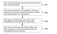
- a method of generating an optical packet is a method of generating an optical packet to be transmitted to an optical receiver from an electric packet input to the optical transmitter by using the optical transmitter and an optical switch, including a step of causing the optical transmitter to convert the electric packet into an optical packet, a step of causing the optical transmitter to demultiplex the optical packet by the number of optical receivers to which the optical packets are transmitted, a step of causing the optical switch to assign time slots to the demultiplexed optical packets, respectively, and a step of causing the optical switch to set guard times before and after a boundary of the time slots between the demultiplexed optical packets.
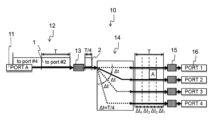
- Fig. 1 is a block diagram showing the arrangement of a switching system according to the first embodiment of the present invention
- Fig. 2 is a view for explaining the operation of the switching system according to the first embodiment of the present invention
- Fig. 3A is a view for explaining the operation of the switching system according to the first embodiment of the present invention
- Fig. 3B is a view for explaining the operation of the switching system according to the first embodiment of the present invention
- Fig. 3C is a view for explaining the operation of the switching system according to the first embodiment of the present invention
- Fig. 3D is a view for explaining the operation of the switching system according to the first embodiment of the present invention
- Fig. 1 is a block diagram showing the arrangement of a switching system according to the first embodiment of the present invention
- Fig. 2 is a view for explaining the operation of the switching system according to the first embodiment of the present invention
- Fig. 3A is a view for explaining the operation of the switching system according to the first embodiment of the present invention
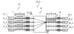
- FIG. 4 is a view for explaining the operation of the switching system according to a modification of the first embodiment of the present invention
- Fig. 5 is a block diagram showing the arrangement of a switching system according to the second embodiment of the present invention
- Fig. 6 is a view for explaining the operation of the switching system according to the second embodiment of the present invention
- Fig. 7 is a flowchart showing a method of generating an optical packet in the switching system according to the second embodiment of the present invention
- Fig. 8 is a view for explaining the operation of a switching system according to a modification of the second embodiment of the present invention
- Fig. 9 is a block diagram showing the arrangement of a switching system according to the third embodiment of the present invention
- Fig. 10 is a flowchart showing a method of generating optical packet in the switching system according to the third embodiment of the present invention
- Fig. 11 is a view for explaining the operation of the switching system according to the third embodiment of the present invention.
- a switching system (packet switching system) 10 sequentially includes input ports 11, input blocks 12, optical transmitters 13, an optical switch 14, optical receivers 15, and output ports 16.
- the optical switch 14 and the optical receiver 15 are connected to an optical fiber 17.
- an optical multiplexer is provided before in the former stage of the optical receiver 15. The multiplexer may multiplex and receive a plurality of optical signals (not shown).
- the input block 12 is an electronic switching unit which is a low-radix switching block (chiplet).
- the input ports 11 of the switching system 10 are branched into m groups, and each group is connected to the input block 12.
- the input block 12 processes an input packet.
- the optical transmitter 13 converts an electric signal output from the input block 12 into an optical signal and outputs the optical signal.
- the optical switch 14 cross-connects the input block 12 and each group of the output port 16 based on an time slot operation (to be described later).
- An optical signal output from the optical switch 14 propagates through the optical fiber 17 and is transmitted to the optical receiver 15.
- the optical receiver 15 converts the optical signal output from the optical switch 14 into an electric signal.
- the output ports 16 of the switching system 10 are divided into m virtual groups.
- the same block is connected to different groups of the different output ports 16 in order, one at a time, and each connection takes place for a time slot (to be described later) where T is a duration of a packet input to the switching system 10.
- the same output port 16 of the input block 12 is always connected to the same output port 16 of the virtual group.
- both the ports have the same index inside the port groups.
- Fig. 2 illustrates the basic operation of the switching system 10 which executes non-block processing using an example of a 4 x 4 switch.
- This switching system 10 is based on a time slot operation to be described below.
- a packet is switched for each input group.
- arbitration is executed within the input packet of the same input group. Since this arbitration is executed for the small number of ports and a low communication amount, the operation can be executed fast without requiring a long time.
- An electric packet 1 input to the switch has a bandwidth BW (bit/sec) and a duration T.
- the desired output port 16 to which the packet is transmitted is set.
- a packet switching operation to any one of the four output ports 16 is complete within the time T. This is because if a time of T or longer is required for the switching of a single packet, the next input packet is blocked and a continuous switching delay is accumulated.
- the optical transmitter 13 compresses the input packet 1 by a factor (in this case, 4) equal in number to the number of ports (that is, the number of optical receivers to which packets are transmitted). That is, the duration of the input packet is divided by a factor equal in number of the number of ports and becomes T/4. In addition, the bandwidth is multiplied by the same factor and becomes 4BW in order to retain the packet data contents.
- a factor in this case, 4
- an optical input packet 2 is generated by satisfying the above conditions.
- the optical switch 14 distributes the respective optical input packets 2 to the desired output ports 16 using periodic time slots.
- the periodic operation of the switch is divided into four time slots.
- the distribution (switching) of the optical input packets 2 is repeatedly executed for each time slot in accordance with a sequence formed by steps S1 to S4 (to be described later).
- the optical receiver 15 converts the packet into an electric packet, and the switching system 10 outputs the electric packet in a predetermined duration.
- the data rate of the signal output from the switching system 10 is equal to the data rate of the input signal.
- the data rate is changed to the first data rate. This change is performed in the arrival order of packets.
- the priority of the change may be set by another arbitration.
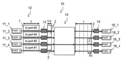
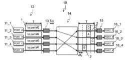
- Figs. 3A to 3D show examples of a series of switching operations in steps S1 to S4, respectively.
- packets are input to four ports 11_1 to 11_4, respectively.
- the packet (packet C) input to the port 11_3 has the desired output port as a port 16_3 and has the highest priority.
- the packets (packets A and D) input to ports 11_1 and 11_4 have the desired ports as ports 16_2 and 16_1, respectively, and have the second highest priority.
- the packet (packet B) input to the port 11_2 has the desired output port as a port 16_4 and has the third highest priority.
- the packet C since the packet C has the highest priority, the packet C is transmitted to the output port 16_3 in a duration of the first time slot (step S1 and Fig. 3A).
- the packets A and D Since the packets A and D have the second highest priority, they are simultaneously transmitted to the output ports 16_2 and 16_1 in a duration of the second time slot (step S2 and Fig. 3B). In this case, since the packets A and D are transmitted to different output ports, no collision occurs.
- the packet (packet B) input to the port B has the third highest priority, it is transferred to the output port 16_4 in a duration of the third time slot (step S3 and Fig. 3C).
- step S3 since transmission of the packets A to D is complete in the previous step (step S3), switching is not executed in a duration of the fourth time slot (step S4 and Fig. 3D).
- the respective output ports 16 are connected to only one input port 11.
- the input port 11 is connected to the desired output port 16.
- the packet is arranged in a correct (accurate) time slot (the divided duration).
- optical receiver 15 in the switching system 10 can be operated in correspondence with this burst mode transmission.
- a high-speed 4 x 4 optical switch device can be easily implemented.
- a time for making one switch form (for example, Fig. 3A) to transition to another switch form (for example, Fig. 3B) is very short as compared with the input packet duration.
- the transition time in an actually usable technique can be reduced to 10 psec and is very short as compared with 100 Gb/s Ethernet packet having a duration of, for example, 120 nsec.
- this guard time is less than 1/10 of the input packet duration.
- the transition time is short to fall within the guard time.
- an input packet passes through an input port of the switch.
- the destination and the priority of the input packet are tested, and then a concentrated arbitration is performed.
- a packet to be transmitted first is determined from all the packets having the same output port as the destination.
- the switching capacity can be increased with the power consumption lower than that of an ASIC made of a CMOS transistor.
- the chiplet is used for the input block 12, the area occupied by the input block 12 can be reduced. As a result, the entire area of the packet switch (chip) will not be increased even if an optical-electrical interface is mounted. Accordingly, the throughput (processing capacity) of the switch can be increased by mounting the optical-electrical interface without changing the chip area. In addition, by using the chiplet, the power consumption can be reduced.
- the contention between the ports of the same block can be prevented, and non-blocking processing can be executed.
- the packets (the packets A to D) are input to the four ports 11_1 to 11_4, respectively.
- the packets A to D have the same desired output port (16_2) and are assigned in the order of B, A, D, and C.
- the packet B since the packet B has the highest priority, the packet B is transmitted to the output port 16_2 in the duration of the first time slot (step S1).
- the packet A since the packet A has the second highest priority, the packet A is transmitted to the output port 16_2 in the duration of the second time slot (step S2).
- the packet D since the packet D has the third highest priority, the packet D is transmitted to the output port 16_2 in the duration of the third time slot (step S3).
- the packet C since the packet C has the fourth highest priority, the packet C is transmitted to the output port 16_2 in the duration of the fourth time slot (step S4).
- the switching system 10_2 according to this modification has the following effect in addition to the effect of the first embodiment.
- the compact copies of the input packets are created at a high data rate, and the compact packets are demultiplexed and transmitted in short time slots. Transmission of the packets to the same destination can be executed within a short time using time interleaving as compared with the actual packet input interval.
- a switching system 20 As shown in Fig. 5, a switching system 20 according to this embodiment includes an optical transmitter 13, an optical switch 14, an optical fiber 17, an optical receiver 15, and a clock unit 21.
- the basic arrangement of the switching system 20 except the clock unit 21 is the same as in the first embodiment.
- a packet is input from a host A (3_1) to the optical transmitter 13, output from the optical receiver 15, and transmitted to a host 1 (4_1).
- the common clock signal is transmitted from the clock unit 21 to the optical transmitter 13 and the optical receiver 15.
- the common clock signal may be transmitted to the optical switch 14.
- the common clock signal to be transmitted includes a copy almost equivalent to the common clock signal.
- the copy almost equivalent to the common clock signal includes an equivalent copy and includes a range where the function of a clock signal (to be described later) in the switching system 20 can be executed.
- a single host is connected to each switch port. For example, a 25-Gb/s packet generated by a source host is converted into a 100-Gb/s optical packet using the optical transmitter 13.
- a packet generated by the source host A (3_1) is demultiplexed by a guard time T grd , and converted into two continuous packets. Then the packets are output.
- a guard time equivalent to 2% of the duration of the optical packet is set.
- the minimum value of T grd will be described later.
- T pkt + T grd the duration of the switched packet, the guard time, and the number of switched packets are given as T pkt , T grd , and N, respectively.
- packets are received by the optical receiver 15 in a period N times (T pkt + T grd ). For example, when receiving four switched packets, the period is four times (T pkt + T grd ).
- the optical receiver 15 receives a packet data bit, a bit timing notification is requested.
- a process for detecting the accurate timing of the input bit and recovering the input packet clock on the reception side requires a long time as compared with the short duration of the assumed packet.
- Table 1 shows setting values in the switching system 20.
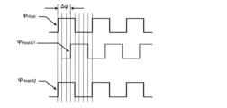
- Fig. 6 shows the mode of clock phases in the switching system 20.
- a clock phase 211 of the input packet does not match a phase 212 of the local copy of the clock shared on the reception side.
- a difference (mismatch) of the initial clock phase can be continuously corrected if the optical path between the optical transmitter 13 and the optical receiver 15 has a time invariant system.
- the clock phase of the input packet can match the clock phase of the optical receiver 15 as the transmission destination (213 in Fig. 6) based on, for example, a phase cache method (K. A. Clark et.al, "Synchronous sub nanosecond clock and data recovery for optically switched data centers using clock phase caching," in Nature Electronics, vol.3, July 2020.)
- a phase cache method K. A. Clark et.al, "Synchronous sub nanosecond clock and data recovery for optically switched data centers using clock phase caching," in Nature Electronics, vol.3, July 2020.
- Fig. 7 shows a flowchart of optical packet transmission/reception including generation of an optical packet using a clock signal in the switching system 20.
- the clock signal is transmitted in advance between the optical transmitter 13 and the optical receiver 15, and a phase (clock phase) of the clock signal is cached (stored) (step S11).
- the optical transmitter 13 demultiplexes the optical packet (the first optical packet) and transmits the demultiplexed optical packet (the first optical packet) to the optical switch 14 using the cached clock phase (step S12).
- the optical switch 14 assigns time slots to the respective demultiplexed optical packets (the first optical packets) and transmits these packets to the optical receiver 15 (step S13).
- the optical receiver 15 measures the phase difference between the clock phase of the optical packet (the first optical packet) received from the optical switch 14 and the clock phase stored in the optical receiver 15 (step S14).
- the optical receiver 15 transmits the measured phase difference to the optical transmitter 13 (step S15).
- the optical transmitter 13 corrects and updates the cached clock phase using the received phase difference (step S16).
- the optical transmitter 13 transmits the next optical packet (the second optical packet) to the optical switch 14 using the updated cached clock phase (step S17).
- the optical switch 14 assigns the time slot to the optical packet (the second optical packet) and transmits it to the optical receiver 15 (step S18).
- the optical receiver 15 receives the optical packet (the second optical packet). As a result, the phase difference becomes zero (step S19).
- the optical transmitter 13 corrects the phase of the data transmitted to the predetermined optical receiver 15 by continuously using the cached clock phase. In this case, in the same optical transmitter 13, different phase correction values are used for the respective destinations.
- the common time reference can be set so as to adjust the data communication in the set time slot without causing collision.
- the data in the burst mode can be received without requiring a long time to recover the clock data.
- a spatial optical fiber having a low temperature sensitivity is used as the optical fiber 17.
- Other arrangements are the same as in the second embodiment.
- a variation in environmental temperature influences the refractive index of the optical fiber 17.
- the already adjusted clock phase can change in the optical receiver 15 serving as the destination after the packet propagates through the fiber 17.
- a variation occurs in a travel time of the packet between the hosts.
- the validity of the value of the corrected cached phase will be examined.
- the frequency depends on a fiber length and a temperature variation pattern in the system environment.
- the switching system 20_1 targets the mutual connection between the hosts arranged at a short distance of about 10 m.
- a 10-m long spatial optical fiber having a low temperature sensitivity is used as the optical fiber 17 to suppress a phase change.
- a switching system 20_2 according to the third modification of this embodiment, as shown in Fig. 8, the end-to-end optical paths between pairs each formed by the optical transmitter 13 and the optical receiver 15 are made equal to each other.
- the lengths of the optical fibers 17 in all combinations each formed by a transmission-side host and a reception-side host are equal to each other.
- Other arrangements are the same as in the second embodiment.
- each of lengths L A1 , L A2 , L A3 , and L A4 of the fibers 17 connecting the host A (3_1) and hosts 1 to 4 (4_1 to 4_4) is about 10 m and includes an error of plus-minus 1 mm
- the maximum value of the difference (T trvl _ Ai_ - T trvl _ Aj ) of the travel times between the fibers (optical paths) 17 is 10 ps which is very small.
- the host unit is connected to the optical switching port and can be arranged regardless of the distance between the hosts.
- each time slot can be occupied by only a target packet without a wrong time slot state of another slot. Therefore, even if the host unit is arranged without any limitation, the appropriate operation of the switching system using the time slot can be ensured.
- the host unit can be arranged without any limitation, and the switching system using the time slot can be appropriately operated.
- optical fibers 17 having the same length are connected to the adjacently arranged units, adjustment can be facilitated, and the optical fibers may be bundled as needed.
- the length of the optical fiber strand can be adjusted at a high resolution by another technique. In this case, if low cost and efficiency in the manufacture of the arranged optical fiber strand are taken into consideration, the resolution can be about plus-minus 1 mm.
- a switching system 30 As shown in Fig. 9, a switching system 30 according to this embodiment sequentially includes optical transmitters 13, optical switches 14, optical fibers 17, an optical multiplexer 31, an optical receiver 15, and a clock unit 21.
- the basic arrangement of the switching system 30 except the clock unit 21 is the same as in the first embodiment.
- Fig. 10 shows a flowchart of the method of generating the optical packet in the switching system 30.
- packets are transmitted from host A (3_1) and host D (3_4) to host 1 (4_1) as the destination host.
- a common clock signal (master) used here is assumed to have an actually used 840-MHz frequency (corresponding to the period of 1.2 nsec).
- a guard time T grd is set before and after a boundary of the time slots between the packets in the optical switch 14 (to be described later).
- phase of the common clock in the optical transmitter 13 of host A (3_1) is slightly different from the phase of the common clock of the optical transmitter 13 of host D (3_4).
- the phase difference of one clock period or more can be perfectly easily detected and corrected (for example, by the time counter).
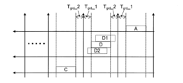
- Fig. 11 shows the mode of packet reception in the optical receiver 15 of host 1 (4_1).
- the optical receiver 15 of host 1 (4_1) assigns the time slot for the reception (packet A) from host A (3_1)
- the time slot is assigned to the reception (packet D) from host D (3_4).
- the time slot is assigned to the reception (packet C) from host C (3_3).
- T grd _1 and T grd _2 are set. More specifically, T grd _1 and T grd _2 are set between the terminal end of the packet A and the start end of the packet D and between the terminal end of the packet D and the start end of the packet C before and after the boundaries (arrows indicated by the solid lines in Fig. 11) of the time slots. In other words, T grd _2 is set at the start end of each packet, and T grd _1 is set at the terminal end of each packet.
- the packet D reaches after the completion of T grd _1 or before the completion of T grd _1. Therefore, even if the packet D reaches as fast as possible, occurrence of the collision with the packet A must be prevented.
- phase clock in the optical transmitter 13 of host D (3_4) is earlier than the phase clock in the optical transmitter 13 of host A (3_1) at the perfectly common clock period, the packet D reaches as fast as possible.
- T grd _2 between the packet A and the packet D that is, T grd _2 at the start end of the packet D is selected to satisfy a condition exceeding the duration of the common clock period, the packet D does not reach within the time slot assigned to the packet A, so that no collision occurs between the packet A and the packet D.
- another method using a burst mode receiver (S.uccint. al, "Hybrid Optoelectronic Router for Future Optical Packet-Switched Networks", Optoelectronics-Advanced Device Structures, 2017) to receive an input data packet in a burst mode without wasting a long time to execute recovery of the clock data may be used.
- the optical clock pulse is generated in synchronism with the input packet in the burst mode.
- This optical clock is used in an operation of a light-triggered specially designed serial/parallel conversion device.
- a demultiplexing clock signal is transmitted together with the data signal and may be used on the reception side.
- the input data can be received fast without requiring an additional process of recovering the clock data.
- the embodiments of the present invention illustrate examples of the structure, size, material, and the like of each constituent component in the arrangements of the switching system and the optical packet transmission apparatus and the method of generating the optical packet.
- the present invention is not limited to this. Any example can be employed as far as the functions of the switching system and the optical packet transmission apparatus and the method of generating the optical packet are enhanced to obtain the same effect as described above.
- the present invention is related to the switching system, the optical packet transmission apparatus, and the method of generating the optical packet and is also applicable to a telephone communication system and a data communication system.
Landscapes
- Engineering & Computer Science (AREA)
- Computer Networks & Wireless Communication (AREA)
- Optical Communication System (AREA)
- Data Exchanges In Wide-Area Networks (AREA)
Abstract
A switching system (10) according to this invention includes a plurality of optical transmitters (13) configured to convert an input electric packet into an optical packet and transmit the optical packet, a plurality of optical receivers (15) configured to receive the optical packet and convert the optical packet into an electric packet, an optical switch (14) arranged between the plurality of optical transmitters and the plurality of optical receivers and configured to transmit the optical packet input from the optical transmitter to any one of the plurality of optical receivers, and a clock unit (21) configured to transmit a clock signal having a clock phase to the optical transmitter and the optical receiver, wherein the clock phase of the optical transmitter is corrected based on a clock phase of the optical packet received by the optical receiver and the clock phase of the optical receiver. Accordingly, this invention can provide a switching system which suppresses collision between optical signals.
Description
The present invention relates to a witching system, an optical packet transmission apparatus, and a method of generating an optical packet, all of which perform switching while suppressing packet collision.
In order to cope with a communication demand highly required in different application domains such as telephone communication and data communication, the bandwidth (bit/sec) of a transmission signal has been greatly increased. Since optical switching can perform switching without converting an optical signal into an electric signal, it can cope with an increase in bandwidth, that is, the communication amount.
In optical switching, optical signals simultaneously sent to the same transmission destination are affected by collision. In conventional electric signal switching, a mechanism for performing buffer processing of data to prevent signal collision is used.
However, in optical switching, a mechanism for performing buffer processing of optical data to prevent optical signal collision has not been implemented yet. For this reason, a switching system including a mechanism for preventing optical signal collision in place of the mechanism for performing buffer processing is necessary.
In order to solve the above problem, a switching system according to the present invention includes a plurality of optical transmitters configured to convert an input electric packet into an optical packet and transmit the optical packet, a plurality of optical receivers configured to receive the optical packet and convert the optical packet into an electric packet, an optical switch arranged between the plurality of optical transmitters and the plurality of optical receivers and configured to transmit the optical packet input from the optical transmitter to any one of the plurality of optical receivers, and a clock unit configured to transmit a clock signal having a clock phase to the optical transmitter and the optical receiver, wherein the clock phase of the optical transmitter is corrected based on a clock phase of the optical packet received by the optical receiver and the clock phase of the optical receiver.
In addition, an optical packet transmission apparatus according to the present invention is an optical packet transmitting apparatus that receives a second electric packet next to a first electric packet, converts the respective packets into optical packets, and transmits the optical packets to an optical receiver based on a clock signal, including an optical transmitter configured to receive the clock signal and store a clock phase of the clock signal, convert the first electric packet into a first optical packet, demultiplex the first optical packet by the number of optical receivers to which the first optical packets are transmitted, and transmit each of the demultiplexed first optical packets in the clock phase, receive, from the optical receiver, a phase difference between a clock phase of the demultiplexed first optical packet received by the optical receiver and a clock phase stored in the optical receiver, and convert the second electric packet into a second optical packet, demultiplex the second optical packet by the number of optical receivers to which the second packets are transmitted, and transmit each of the demultiplexed second optical packets in the phase-corrected clock phase, and an optical switch configured to assign time slots in the demultiplexed first optical packets and the demultiplexed second optical packets, and set guard times before and after a boundary of each of the time slots.
In addition, a method of generating an optical packet according to the present invention is a method of generating, based on a clock signal, an optical packet to be transmitted from an optical transmitter to an optical receiver via an optical switch, including a step of causing the optical transmitter to receive the clock signal and store a clock phase of the clock signal, a step of causing the optical transmitter to demultiplex the first optical packet and transmit each demultiplexed first optical packet in the clock phase, a step of causing the optical switch to assign time slots to the demultiplexed first optical packets, respectively, and transmit the demultiplexed first optical packets, a step of causing the optical receiver to measure a phase difference between a clock phase of each demultiplexed first optical packet and a clock phase stored in the optical receiver, a step of causing the optical receiver to transmit the phase difference to the optical transmitter, a step of causing the optical transmitter to correct a clock phase stored in the optical transmitter by using the phase difference, and a step of causing the optical transmitter to demultiplex the second optical packet and transmit each demultiplexed second optical packet in the corrected clock phase.
In addition, a method of generating an optical packet according to the present invention is a method of generating an optical packet to be transmitted to an optical receiver from an electric packet input to the optical transmitter by using the optical transmitter and an optical switch, including a step of causing the optical transmitter to convert the electric packet into an optical packet, a step of causing the optical transmitter to demultiplex the optical packet by the number of optical receivers to which the optical packets are transmitted, a step of causing the optical switch to assign time slots to the demultiplexed optical packets, respectively, and a step of causing the optical switch to set guard times before and after a boundary of the time slots between the demultiplexed optical packets.
According to the present invention, there are provided a high-speed lower power consumption switching apparatus and a switching method.
(First Embodiment)
A switching system according to the first embodiment of the present invention will be described with reference to Figs. 1 to 4.
A switching system according to the first embodiment of the present invention will be described with reference to Figs. 1 to 4.
(Arrangement of Switching System)
As shown in Fig. 1, a switching system (packet switching system) 10 according to an embodiment sequentially includesinput ports 11, input blocks 12, optical transmitters 13, an optical switch 14, optical receivers 15, and output ports 16. The optical switch 14 and the optical receiver 15 are connected to an optical fiber 17. In addition, an optical multiplexer is provided before in the former stage of the optical receiver 15. The multiplexer may multiplex and receive a plurality of optical signals (not shown).
As shown in Fig. 1, a switching system (packet switching system) 10 according to an embodiment sequentially includes
The input block 12 is an electronic switching unit which is a low-radix switching block (chiplet).
The input ports 11 of the switching system 10 are branched into m groups, and each group is connected to the input block 12.
The input block 12 processes an input packet.
The optical transmitter 13 converts an electric signal output from the input block 12 into an optical signal and outputs the optical signal.
The optical switch 14 cross-connects the input block 12 and each group of the output port 16 based on an time slot operation (to be described later).
An optical signal output from the optical switch 14 propagates through the optical fiber 17 and is transmitted to the optical receiver 15.
The optical receiver 15 converts the optical signal output from the optical switch 14 into an electric signal.
The output ports 16 of the switching system 10 are divided into m virtual groups.
In the switching system 10, the same block is connected to different groups of the different output ports 16 in order, one at a time, and each connection takes place for a time slot (to be described later) where T is a duration of a packet input to the switching system 10.

The same output port 16 of the input block 12 is always connected to the same output port 16 of the virtual group. In this case, both the ports have the same index inside the port groups.
(Operation of Switching System)
The operation of the switching apparatus (packet switch) 10 according to this embodiment will be described with reference to Fig. 2.
The operation of the switching apparatus (packet switch) 10 according to this embodiment will be described with reference to Fig. 2.
Fig. 2 illustrates the basic operation of the switching system 10 which executes non-block processing using an example of a 4 x 4 switch. This switching system 10 is based on a time slot operation to be described below.
First, a packet is switched for each input group. In this case, arbitration is executed within the input packet of the same input group. Since this arbitration is executed for the small number of ports and a low communication amount, the operation can be executed fast without requiring a long time.
An electric packet 1 input to the switch has a bandwidth BW (bit/sec) and a duration T. The desired output port 16 to which the packet is transmitted is set.
In the switching system 10, a packet switching operation to any one of the four output ports 16 is complete within the time T. This is because if a time of T or longer is required for the switching of a single packet, the next input packet is blocked and a continuous switching delay is accumulated.
In order to match the input packet 1 with the time slot, the optical transmitter 13 compresses the input packet 1 by a factor (in this case, 4) equal in number to the number of ports (that is, the number of optical receivers to which packets are transmitted). That is, the duration of the input packet is divided by a factor equal in number of the number of ports and becomes T/4. In addition, the bandwidth is multiplied by the same factor and becomes 4BW in order to retain the packet data contents.
As described above, an optical input packet 2 is generated by satisfying the above conditions.
Next, the optical switch 14 distributes the respective optical input packets 2 to the desired output ports 16 using periodic time slots. In this case, the periodic operation of the switch is divided into four time slots.

The distribution (switching) of the optical input packets 2 is repeatedly executed for each time slot in accordance with a sequence formed by steps S1 to S4 (to be described later).
Finally, the optical receiver 15 converts the packet into an electric packet, and the switching system 10 outputs the electric packet in a predetermined duration. In other words, the data rate of the signal output from the switching system 10 is equal to the data rate of the input signal.
In the packets arriving in different time slots whose time difference is reduced, the data rate is changed to the first data rate. This change is performed in the arrival order of packets. In addition, the priority of the change may be set by another arbitration.
The switching operation in the above optical switch 14 will be described with reference to Figs. 3A to 3D. Figs. 3A to 3D show examples of a series of switching operations in steps S1 to S4, respectively.
In the switching system 10, packets are input to four ports 11_1 to 11_4, respectively. The packet (packet C) input to the port 11_3 has the desired output port as a port 16_3 and has the highest priority.
The packets (packets A and D) input to ports 11_1 and 11_4 have the desired ports as ports 16_2 and 16_1, respectively, and have the second highest priority.
The packet (packet B) input to the port 11_2 has the desired output port as a port 16_4 and has the third highest priority.
First, since the packet C has the highest priority, the packet C is transmitted to the output port 16_3 in a duration of the first time slot (step S1 and Fig. 3A).
Since the packets A and D have the second highest priority, they are simultaneously transmitted to the output ports 16_2 and 16_1 in a duration of the second time slot (step S2 and Fig. 3B). In this case, since the packets A and D are transmitted to different output ports, no collision occurs.
Next, since the packet (packet B) input to the port B has the third highest priority, it is transferred to the output port 16_4 in a duration of the third time slot (step S3 and Fig. 3C).
Finally, since transmission of the packets A to D is complete in the previous step (step S3), switching is not executed in a duration of the fourth time slot (step S4 and Fig. 3D).

As described above, if the operation cycle (the four steps) is complete, all the input packets are simultaneously switched to desired output ports by the non-blocking method.
In this switching operation, in all the steps, as shown in Figs. 3A to 3D, the respective output ports 16 are connected to only one input port 11. In addition, the input port 11 is connected to the desired output port 16. In switching of the packet input to the input port 11, the packet is arranged in a correct (accurate) time slot (the divided duration).
In addition, the optical receiver 15 in the switching system 10 can be operated in correspondence with this burst mode transmission.
When the switching system 10 is formed by four 1 x 4 switching units corresponding to the different input ports 11, a high-speed 4 x 4 optical switch device can be easily implemented. In the 4 x 4 optical switch device, a time for making one switch form (for example, Fig. 3A) to transition to another switch form (for example, Fig. 3B) is very short as compared with the input packet duration.
For example, if it is assumed that the transition time can be neglected, the transition time in an actually usable technique can be reduced to 10 psec and is very short as compared with 100 Gb/s Ethernet packet having a duration of, for example, 120 nsec.
In addition, if a short guard time is set between the packets input to the same input port 11 to avoid the data loss between the switching operations, this guard time is less than 1/10 of the input packet duration. The transition time is short to fall within the guard time.
(Effect)
An effect of theswitching system 10 according to this embodiment will be described below.
An effect of the
In a normal electric switch, an input packet passes through an input port of the switch. The destination and the priority of the input packet are tested, and then a concentrated arbitration is performed. A packet to be transmitted first is determined from all the packets having the same output port as the destination.
Execution of the concentrated arbitration process is complicated with an increase in the number of switch ports and the throughput. As a result, the communication latency and the power consumption increase.
On the other hand, since switching system can be performed without executing the concentrated arbitration requiring a long time according to the switching apparatus (packet switch) of this embodiment, the communication latency and the power consumption can decrease.
Since the optical switch is in charge of part of the switching processing, the switching capacity can be increased with the power consumption lower than that of an ASIC made of a CMOS transistor.
In addition, since the chiplet is used for the input block 12, the area occupied by the input block 12 can be reduced. As a result, the entire area of the packet switch (chip) will not be increased even if an optical-electrical interface is mounted. Accordingly, the throughput (processing capacity) of the switch can be increased by mounting the optical-electrical interface without changing the chip area. In addition, by using the chiplet, the power consumption can be reduced.
In addition, the contention between the ports of the same block can be prevented, and non-blocking processing can be executed.
(First Modification)
A switching system according to the first modification of the first embodiment of the present invention will be described with reference to Fig. 4. The arrangement of a switching system 10_2 according to this modification is the same as that of the first embodiment.
A switching system according to the first modification of the first embodiment of the present invention will be described with reference to Fig. 4. The arrangement of a switching system 10_2 according to this modification is the same as that of the first embodiment.
(Operation of Switching System)
The operation of the switching system 10_2 according to this modification will be described below.
The operation of the switching system 10_2 according to this modification will be described below.
In the switching system 10_2, the packets (the packets A to D) are input to the four ports 11_1 to 11_4, respectively. The packets A to D have the same desired output port (16_2) and are assigned in the order of B, A, D, and C.
First, since the packet B has the highest priority, the packet B is transmitted to the output port 16_2 in the duration of the first time slot (step S1).
Next, since the packet A has the second highest priority, the packet A is transmitted to the output port 16_2 in the duration of the second time slot (step S2).
Next, since the packet D has the third highest priority, the packet D is transmitted to the output port 16_2 in the duration of the third time slot (step S3).
Finally, since the packet C has the fourth highest priority, the packet C is transmitted to the output port 16_2 in the duration of the fourth time slot (step S4).
As described above, if the operation cycle (the four steps) is complete, all the input packets are simultaneously switched to desired output ports by the non-blocking method. In this case, since the packets A to D are transmitted in the different time slots, no collision occurs.
As described above, in the switching system 10_2, all the input ports to be transmitted to the same output port are correctly (accurately) switched to this output port in the time T.
(Effect)
The switching system 10_2 according to this modification has the following effect in addition to the effect of the first embodiment.
The switching system 10_2 according to this modification has the following effect in addition to the effect of the first embodiment.
When simultaneously transmitting a plurality of packets to the same destination in the conventional packet switch, parallel optical receivers equal in number of the number of packets are required.
In the switching system 10_2, the compact copies of the input packets are created at a high data rate, and the compact packets are demultiplexed and transmitted in short time slots. Transmission of the packets to the same destination can be executed within a short time using time interleaving as compared with the actual packet input interval.
According to the switching system of this modification, since the packets can be transmitted to the same output port without executing the concentrated arbitration requiring a long time, thereby reducing the communication latency and the power consumption.
(Second Embodiment)
A switching system according to the second embodiment of the present invention will be described with reference to Figs. 5 to 7.
A switching system according to the second embodiment of the present invention will be described with reference to Figs. 5 to 7.
(Arrangement of Switching System)
As shown in Fig. 5, aswitching system 20 according to this embodiment includes an optical transmitter 13, an optical switch 14, an optical fiber 17, an optical receiver 15, and a clock unit 21. The basic arrangement of the switching system 20 except the clock unit 21 is the same as in the first embodiment.
As shown in Fig. 5, a
A packet is input from a host A (3_1) to the optical transmitter 13, output from the optical receiver 15, and transmitted to a host 1 (4_1).
(Operation of Switching System)
The operation using a common clock signal in theswitching system 20 according to this embodiment will be described with reference to Fig. 5.
The operation using a common clock signal in the
In the switching system 20, the common clock signal is transmitted from the clock unit 21 to the optical transmitter 13 and the optical receiver 15. Alternatively, the common clock signal may be transmitted to the optical switch 14. In this case, the common clock signal to be transmitted includes a copy almost equivalent to the common clock signal. The copy almost equivalent to the common clock signal includes an equivalent copy and includes a range where the function of a clock signal (to be described later) in the switching system 20 can be executed.
A single host is connected to each switch port. For example, a 25-Gb/s packet generated by a source host is converted into a 100-Gb/s optical packet using the optical transmitter 13.
At the optical transmitter 13, a packet generated by the source host A (3_1) is demultiplexed by a guard time Tgrd, and converted into two continuous packets. Then the packets are output.
If the time of the start end of the first packet in a duration Tpkt of the switched packet is given as zero, the terminal end of the first packet is Tpkt, and the time of the start end of the next packet is Tpkt + Tgrd, and its terminal end is 2Tpkt + Tgrd.
For example, a guard time equivalent to 2% of the duration of the optical packet is set. The minimum value of Tgrd will be described later.
If it is assumed that the duration of the switched packet, the guard time, and the number of switched packets are given as Tpkt, Tgrd, and N, respectively, packets are received by the optical receiver 15 in a period N times (Tpkt + Tgrd). For example, when receiving four switched packets, the period is four times (Tpkt + Tgrd).
If the optical receiver 15 receives a packet data bit, a bit timing notification is requested. Conventionally, a process for detecting the accurate timing of the input bit and recovering the input packet clock on the reception side requires a long time as compared with the short duration of the assumed packet.
By sharing an optical clock between the optical transmitter 13 and the optical receiver 15, the process requiring a long time can be prevented.
Table 1 shows setting values in the switching system 20.
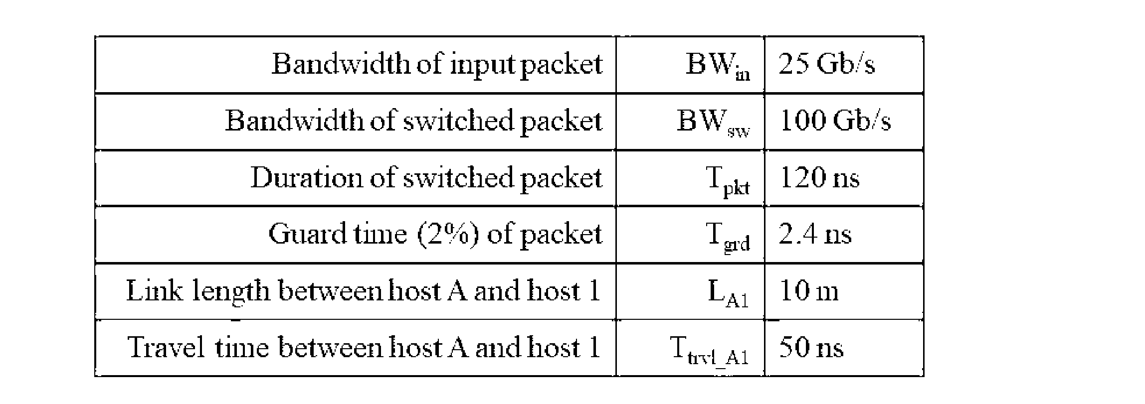
Fig. 6 shows the mode of clock phases in the switching system 20.
Even if the clock is generally shared, a clock phase 211 of the input packet does not match a phase 212 of the local copy of the clock shared on the reception side. A difference (mismatch) of the initial clock phase can be continuously corrected if the optical path between the optical transmitter 13 and the optical receiver 15 has a time invariant system.

However, for example, if packets from the optical transmitter 13 can reach the same optical receiver 15 via unknown randomly selected optical paths, the optical paths between the optical transmitter 13 and the optical receiver 15 cannot be phase-adjusted because they do not have the time variant system.
In the switching system 20, the clock phase of the input packet can match the clock phase of the optical receiver 15 as the transmission destination (213 in Fig. 6) based on, for example, a phase cache method (K. A. Clark et.al, "Synchronous sub nanosecond clock and data recovery for optically switched data centers using clock phase caching," in Nature Electronics, vol.3, July 2020.)
Fig. 7 shows a flowchart of optical packet transmission/reception including generation of an optical packet using a clock signal in the switching system 20.
The clock signal is transmitted in advance between the optical transmitter 13 and the optical receiver 15, and a phase (clock phase) of the clock signal is cached (stored) (step S11).
First, the optical transmitter 13 demultiplexes the optical packet (the first optical packet) and transmits the demultiplexed optical packet (the first optical packet) to the optical switch 14 using the cached clock phase (step S12).
Next, the optical switch 14 assigns time slots to the respective demultiplexed optical packets (the first optical packets) and transmits these packets to the optical receiver 15 (step S13).
Next, the optical receiver 15 measures the phase difference between the clock phase of the optical packet (the first optical packet) received from the optical switch 14 and the clock phase stored in the optical receiver 15 (step S14).
Next, the optical receiver 15 transmits the measured phase difference to the optical transmitter 13 (step S15).
Next, the optical transmitter 13 corrects and updates the cached clock phase using the received phase difference (step S16).
Next, the optical transmitter 13 transmits the next optical packet (the second optical packet) to the optical switch 14 using the updated cached clock phase (step S17).
Next, the optical switch 14 assigns the time slot to the optical packet (the second optical packet) and transmits it to the optical receiver 15 (step S18).
Finally, the optical receiver 15 receives the optical packet (the second optical packet). As a result, the phase difference becomes zero (step S19).
As described above, the optical transmitter 13 corrects the phase of the data transmitted to the predetermined optical receiver 15 by continuously using the cached clock phase. In this case, in the same optical transmitter 13, different phase correction values are used for the respective destinations.
According to this embodiment, by sharing the clock signal, the common time reference can be set so as to adjust the data communication in the set time slot without causing collision. In addition, the data in the burst mode can be received without requiring a long time to recover the clock data.
(Second Modification)
In a switching system 20_1 according to the second modification of this embodiment, a spatial optical fiber having a low temperature sensitivity is used as theoptical fiber 17. Other arrangements are the same as in the second embodiment.
In a switching system 20_1 according to the second modification of this embodiment, a spatial optical fiber having a low temperature sensitivity is used as the

In the switching system 20_1, a variation in environmental temperature influences the refractive index of the optical fiber 17. In a packet to be transmitted, the already adjusted clock phase can change in the optical receiver 15 serving as the destination after the packet propagates through the fiber 17. As a result, a variation (fluctuation) occurs in a travel time of the packet between the hosts.
In the switching system 20_1, the validity of the value of the corrected cached phase will be examined. In this case, the frequency depends on a fiber length and a temperature variation pattern in the system environment.
As described above, the switching system 20_1 targets the mutual connection between the hosts arranged at a short distance of about 10 m. A 10-m long spatial optical fiber having a low temperature sensitivity is used as the optical fiber 17 to suppress a phase change.

Accordingly, for example, if the clock phase is initially adjusted at the activation of the switching system, a long-time operation can be performed without requiring further correction.
According to the switching system of this modification, the variation of the clock phase by the temperature change can be suppressed.
(Third Modification)
In a switching system 20_2 according to the third modification of this embodiment, as shown in Fig. 8, the end-to-end optical paths between pairs each formed by theoptical transmitter 13 and the optical receiver 15 are made equal to each other. In other words, the lengths of the optical fibers 17 in all combinations each formed by a transmission-side host and a reception-side host (that is, the optical switch 14 and the optical receiver 15) are equal to each other. Other arrangements are the same as in the second embodiment.
In a switching system 20_2 according to the third modification of this embodiment, as shown in Fig. 8, the end-to-end optical paths between pairs each formed by the
For example, if each of lengths LA1, LA2, LA3, and LA4 of the fibers 17 connecting the host A (3_1) and hosts 1 to 4 (4_1 to 4_4) is about 10 m and includes an error of plus-minus 1 mm, the maximum value of the difference (Ttrvl_Ai_ - Ttrvl_Aj) of the travel times between the fibers (optical paths) 17 is 10 ps which is very small.
In the switching system 20_2, the host unit is connected to the optical switching port and can be arranged regardless of the distance between the hosts.
In the switching system 20_2 according to this modification, each time slot can be occupied by only a target packet without a wrong time slot state of another slot. Therefore, even if the host unit is arranged without any limitation, the appropriate operation of the switching system using the time slot can be ensured.
According to the switching system of this modification, the host unit can be arranged without any limitation, and the switching system using the time slot can be appropriately operated.
According to this modification, since the optical fibers 17 having the same length are connected to the adjacently arranged units, adjustment can be facilitated, and the optical fibers may be bundled as needed.
The length of the optical fiber strand can be adjusted at a high resolution by another technique. In this case, if low cost and efficiency in the manufacture of the arranged optical fiber strand are taken into consideration, the resolution can be about plus-minus 1 mm.
(Third Embodiment)
A switching system according to the third embodiment of the present invention will be described with reference to Figs. 9 to 11.
A switching system according to the third embodiment of the present invention will be described with reference to Figs. 9 to 11.
(Arrangement of Switching System)
As shown in Fig. 9, aswitching system 30 according to this embodiment sequentially includes optical transmitters 13, optical switches 14, optical fibers 17, an optical multiplexer 31, an optical receiver 15, and a clock unit 21. The basic arrangement of the switching system 30 except the clock unit 21 is the same as in the first embodiment.
As shown in Fig. 9, a
(Method of Generating Optical Packet)
A method of generating an optical packet in theswitching system 30 according to this embodiment will be described below.
A method of generating an optical packet in the
Fig. 10 shows a flowchart of the method of generating the optical packet in the switching system 30.
For example, as shown in Fig. 9, in the switching system 30, packets are transmitted from host A (3_1) and host D (3_4) to host 1 (4_1) as the destination host.
A common clock signal (master) used here is assumed to have an actually used 840-MHz frequency (corresponding to the period of 1.2 nsec).
For the packet to be transmitted from host A (3_1), a guard time Tgrd is set before and after a boundary of the time slots between the packets in the optical switch 14 (to be described later). As a result, if the duration of the switched packet is given as Tpkt, and the time of the start end of the first packet is zero, the time of the start end of the next packet is Tpkt + Tgrd, and the start end of the subsequent packet becomes twice (Tpkt + Tgrd).
Similarly, a packet is transmitted from host D (3_4).
At this time, the phase of the common clock in the optical transmitter 13 of host A (3_1) is slightly different from the phase of the common clock of the optical transmitter 13 of host D (3_4).

The phase difference of one clock period or more can be perfectly easily detected and corrected (for example, by the time counter).
Fig. 11 shows the mode of packet reception in the optical receiver 15 of host 1 (4_1).
After the optical receiver 15 of host 1 (4_1) assigns the time slot for the reception (packet A) from host A (3_1), the time slot is assigned to the reception (packet D) from host D (3_4). Subsequently, the time slot is assigned to the reception (packet C) from host C (3_3).
After the packet A, signal-free guard times Tgrd_1 and Tgrd_2 are set. More specifically, Tgrd_1 and Tgrd_2 are set between the terminal end of the packet A and the start end of the packet D and between the terminal end of the packet D and the start end of the packet C before and after the boundaries (arrows indicated by the solid lines in Fig. 11) of the time slots. In other words, Tgrd_2 is set at the start end of each packet, and Tgrd_1 is set at the terminal end of each packet.
If the clock phases of host A (3_1) and host D (3_4) perfectly match each other, the packet D (from host D) accurately reaches the light receiver 15 of host 1 (4_1) at the terminal end of guard time Tgrd.
However, since the phase difference generally occurs between the packet A and the packet D, the packet D reaches after the completion of Tgrd_1 or before the completion of Tgrd_1. Therefore, even if the packet D reaches as fast as possible, occurrence of the collision with the packet A must be prevented.
If the phase clock in the optical transmitter 13 of host D (3_4) is earlier than the phase clock in the optical transmitter 13 of host A (3_1) at the perfectly common clock period, the packet D reaches as fast as possible.

If at least the guide time Tgrd_2 between the packet A and the packet D, that is, Tgrd_2 at the start end of the packet D is selected to satisfy a condition exceeding the duration of the common clock period, the packet D does not reach within the time slot assigned to the packet A, so that no collision occurs between the packet A and the packet D.
If the start end of the packet D falls within Tgrd_2 even if the packet D reaches earlier, no collision occurs between the packet A and the packet D (a rectangle D1 indicated by a dotted line in Fig. 11).
In addition, similarly, collision with the packet C must be prevented even if the packet D reaches as fast as possible. If at least guard time Tgrd_1 between the packet D and the packet C, that is, if Tgrd_1 at the terminal end of the packet D is selected to satisfy a condition exceeding the duration of the common clock period, the packet D does not reach within the time slot assigned to the packet C, so collision between the packet D and the packet C does not occur.
If the terminal end of the packet D falls within Tgrd_1 even if the packet D reaches with a delay, no collision occurs between the packet D and the packet C (a rectangle D2 indicated by a dotted line in Fig. 11).
As described above, by setting the guard times between the packets to exceed the common clock phase differences between the packets, collision can be prevented between different packets.
According to this embodiment, by sharing the clock signal and setting the guard time, occurrence of the collision can further be suppressed, and the packet can be switched and transmitted/received.
According to this embodiment, another method using a burst mode receiver (S. Ibrahim et. al, "Hybrid Optoelectronic Router for Future Optical Packet-Switched Networks", Optoelectronics-Advanced Device Structures, 2017) to receive an input data packet in a burst mode without wasting a long time to execute recovery of the clock data may be used. In this case, the optical clock pulse is generated in synchronism with the input packet in the burst mode. This optical clock is used in an operation of a light-triggered specially designed serial/parallel conversion device.
According to this embodiment of the present invention, a demultiplexing clock signal is transmitted together with the data signal and may be used on the reception side. By maintaining synchronization between the clock signal and the data signal up to the reception side, the input data can be received fast without requiring an additional process of recovering the clock data.
The embodiments of the present invention illustrate examples of the structure, size, material, and the like of each constituent component in the arrangements of the switching system and the optical packet transmission apparatus and the method of generating the optical packet. However, the present invention is not limited to this. Any example can be employed as far as the functions of the switching system and the optical packet transmission apparatus and the method of generating the optical packet are enhanced to obtain the same effect as described above.
The present invention is related to the switching system, the optical packet transmission apparatus, and the method of generating the optical packet and is also applicable to a telephone communication system and a data communication system.
10: switching system
13: optical transmitter
14: optical switch
15: optical receiver
21: clock unit
13: optical transmitter
14: optical switch
15: optical receiver
21: clock unit
Claims (8)
- A switching system comprising:
a plurality of optical transmitters configured to convert an input electric packet into an optical packet and transmit the optical packet;
a plurality of optical receivers configured to receive the optical packet and convert the optical packet into an electric packet;
an optical switch arranged between the plurality of optical transmitters and the plurality of optical receivers and configured to transmit the optical packet input from the optical transmitter to any one of the plurality of optical receivers; and
a clock unit configured to transmit a clock signal having a clock phase to the optical transmitter and the optical receiver,
wherein the clock phase of the optical transmitter is corrected based on a clock phase of the optical packet received by the optical receiver and the clock phase of the optical receiver. - The switching system according to claim 1, further comprising an optical fiber configured to connect the optical switch and the optical transmitter,
wherein the optical fiber has a low temperature sensitivity. - The switching system according to claim 1, further comprising a plurality of optical fibers configured to connect the optical switch and the optical transmitter,
wherein the plurality of optical fibers are made to equal to each other. - The switching system according to claim 1, wherein
the optical transmitter demultiplexes the optical packet in a number equal to the number of optical receivers to which the optical packets are transmitted, and
the optical switch transmits the demultiplexed optical packets in time slots respectively assigned to the demultiplexed optical packets. - The switching system according to claim 4, wherein the optical switch sets guard times before and after a boundary of the time slot.
- An optical packet transmitting apparatus that receives a second electric packet next to a first electric packet, converts the respective packets into optical packets, and transmits the optical packets to an optical receiver based on a clock signal, comprising:
an optical transmitter configured to
receive the clock signal and store a clock phase of the clock signal,
convert the first electric packet into a first optical packet, demultiplex the first optical packet by the number of optical receivers to which the first optical packets are transmitted, and transmit each of the demultiplexed first optical packets in the clock phase,
receive, from the optical receiver, a phase difference between a clock phase of the demultiplexed first optical packet received by the optical receiver and a clock phase stored in the optical receiver, and
convert the second electric packet into a second optical packet, demultiplex the second optical packet by the number of optical receivers to which the second packets are transmitted, and transmit each of the demultiplexed second optical packets in the phase-corrected clock phase; and
an optical switch configured to
assign time slots in the demultiplexed first optical packets and the demultiplexed second optical packets, and set guard times before and after a boundary of each of the time slots. - A method of generating, based on a clock signal, an optical packet to be transmitted from an optical transmitter to an optical receiver via an optical switch, comprising:
a step of causing the optical transmitter and the optical receiver to receive the clock signal and store a clock phase of the clock signal;
a step of causing the optical transmitter to demultiplex the first optical packet and transmit each demultiplexed first optical packet in the clock phase;
a step of causing the optical switch to assign time slots to the demultiplexed first optical packets, respectively, and transmit the demultiplexed first optical packets;
a step of causing the optical receiver to measure a phase difference between a clock phase of each demultiplexed first optical packet and a clock phase stored in the optical receiver;
a step of causing the optical receiver to transmit the phase difference to the optical transmitter;
a step of causing the optical transmitter to correct a clock phase stored in the optical transmitter by using the phase difference; and
a step of causing the optical transmitter to demultiplex the second optical packet and transmit each demultiplexed second optical packet in the corrected clock phase. - A method of generating an optical packet to be transmitted to an optical receiver from an electric packet input to the optical transmitter by using the optical transmitter and an optical switch, comprising:
a step of causing the optical transmitter to convert the electric packet into an optical packet;
a step of causing the optical transmitter to demultiplex the optical packet by the number of optical receivers to which the optical packets are transmitted;
a step of causing the optical switch to assign time slots to the demultiplexed optical packets, respectively; and
a step of causing the optical switch to set guard times before and after a boundary of the time slots between the demultiplexed optical packets.
Priority Applications (2)
| Application Number | Priority Date | Filing Date | Title |
|---|---|---|---|
| JP2025508488A JP7750450B2 (en) | 2022-08-18 | 2022-08-18 | Switching system, optical packet transmitter, and optical packet generation method |
| PCT/JP2022/031219 WO2024038540A1 (en) | 2022-08-18 | 2022-08-18 | Switching system, optical packet transmission apparatus, and method of generating optical packet |
Applications Claiming Priority (1)
| Application Number | Priority Date | Filing Date | Title |
|---|---|---|---|
| PCT/JP2022/031219 WO2024038540A1 (en) | 2022-08-18 | 2022-08-18 | Switching system, optical packet transmission apparatus, and method of generating optical packet |
Publications (1)
| Publication Number | Publication Date |
|---|---|
| WO2024038540A1 true WO2024038540A1 (en) | 2024-02-22 |
Family
ID=89941476
Family Applications (1)
| Application Number | Title | Priority Date | Filing Date |
|---|---|---|---|
| PCT/JP2022/031219 Ceased WO2024038540A1 (en) | 2022-08-18 | 2022-08-18 | Switching system, optical packet transmission apparatus, and method of generating optical packet |
Country Status (2)
| Country | Link |
|---|---|
| JP (1) | JP7750450B2 (en) |
| WO (1) | WO2024038540A1 (en) |
Citations (3)
| Publication number | Priority date | Publication date | Assignee | Title |
|---|---|---|---|---|
| JPH10243017A (en) * | 1997-02-26 | 1998-09-11 | Nec Corp | Optical network control system and optical network |
| US6441935B1 (en) * | 1997-12-12 | 2002-08-27 | Nec Corporation | Optical packet exchange system and optical switch |
| JP2011019122A (en) * | 2009-07-09 | 2011-01-27 | Oki Electric Industry Co Ltd | Optical code label switch method and optical code label switch device |
-
2022
- 2022-08-18 WO PCT/JP2022/031219 patent/WO2024038540A1/en not_active Ceased
- 2022-08-18 JP JP2025508488A patent/JP7750450B2/en active Active
Patent Citations (3)
| Publication number | Priority date | Publication date | Assignee | Title |
|---|---|---|---|---|
| JPH10243017A (en) * | 1997-02-26 | 1998-09-11 | Nec Corp | Optical network control system and optical network |
| US6441935B1 (en) * | 1997-12-12 | 2002-08-27 | Nec Corporation | Optical packet exchange system and optical switch |
| JP2011019122A (en) * | 2009-07-09 | 2011-01-27 | Oki Electric Industry Co Ltd | Optical code label switch method and optical code label switch device |
Also Published As
| Publication number | Publication date |
|---|---|
| JP7750450B2 (en) | 2025-10-07 |
| JP2025526139A (en) | 2025-08-07 |
Similar Documents
| Publication | Publication Date | Title |
|---|---|---|
| US6711357B1 (en) | Timing and synchronization for an IP router using an optical switch | |
| US6760346B1 (en) | Packet switching network | |
| US7463626B2 (en) | Phase and frequency drift and jitter compensation in a distributed telecommunications switch | |
| US5251210A (en) | Method and apparatus for transforming low bandwidth telecommunications channels into a high bandwidth telecommunication channel | |
| CN1086878C (en) | Synchronisation in digital communications networks | |
| US7127645B2 (en) | Skew compensation method | |
| EP1965601B1 (en) | Optical transmission system and optical transmission method | |
| US7130317B2 (en) | Method and circuit for de-skewing data in a communication system | |
| US8019228B2 (en) | Optical switching transmission system with timing correction | |
| US7835649B2 (en) | Optical data synchronization scheme | |
| CN101552766A (en) | Deskew device and method applied to high-speed parallel optical interconnection system | |
| WO2024038540A1 (en) | Switching system, optical packet transmission apparatus, and method of generating optical packet | |
| WO2014013601A1 (en) | Transmission device | |
| CA2337742C (en) | Hyper-concatenation across multiple parallel channels | |
| CN104023281A (en) | System and method for data flow identification and alignment | |
| EP1158711A2 (en) | Concatenation across independent pointed processors | |
| JP2010016705A (en) | Transmission system and transmission method | |
| US12476782B2 (en) | Systems and methods for synchronizing network nodes | |
| US7317720B2 (en) | Signal transmission system | |
| JP2001069105A (en) | How to send a concatenated signal | |
| White et al. | Design of a control-channel-based media-access-control protocol for HORNET | |
| WO2024038539A1 (en) | Switching apparatus and switching method | |
| US20250294275A1 (en) | Apparatus and method for acquiring data synchronization in passive optical network | |
| EP4016428A1 (en) | Data processing device and system | |
| CN113794956A (en) | Method and device for optical packet switching |
Legal Events
| Date | Code | Title | Description |
|---|---|---|---|
| 121 | Ep: the epo has been informed by wipo that ep was designated in this application |
Ref document number: 22955714 Country of ref document: EP Kind code of ref document: A1 |
|
| WWE | Wipo information: entry into national phase |
Ref document number: 2025508488 Country of ref document: JP |
|
| NENP | Non-entry into the national phase |
Ref country code: DE |
|
| 122 | Ep: pct application non-entry in european phase |
Ref document number: 22955714 Country of ref document: EP Kind code of ref document: A1 |