WO2024038511A1 - 半導体装置および半導体装置の製造方法 - Google Patents
半導体装置および半導体装置の製造方法 Download PDFInfo
- Publication number
- WO2024038511A1 WO2024038511A1 PCT/JP2022/031026 JP2022031026W WO2024038511A1 WO 2024038511 A1 WO2024038511 A1 WO 2024038511A1 JP 2022031026 W JP2022031026 W JP 2022031026W WO 2024038511 A1 WO2024038511 A1 WO 2024038511A1
- Authority
- WO
- WIPO (PCT)
- Prior art keywords
- circuit pattern
- electrode terminal
- semiconductor device
- protrusion
- fitting
- Prior art date
- Legal status (The legal status is an assumption and is not a legal conclusion. Google has not performed a legal analysis and makes no representation as to the accuracy of the status listed.)
- Ceased
Links
Images


Classifications
-
- H—ELECTRICITY
- H10—SEMICONDUCTOR DEVICES; ELECTRIC SOLID-STATE DEVICES NOT OTHERWISE PROVIDED FOR
- H10W—GENERIC PACKAGES, INTERCONNECTIONS, CONNECTORS OR OTHER CONSTRUCTIONAL DETAILS OF DEVICES COVERED BY CLASS H10
- H10W90/00—Package configurations
- H10W90/701—Package configurations characterised by the relative positions of pads or connectors relative to package parts
-
- H—ELECTRICITY
- H10—SEMICONDUCTOR DEVICES; ELECTRIC SOLID-STATE DEVICES NOT OTHERWISE PROVIDED FOR
- H10W—GENERIC PACKAGES, INTERCONNECTIONS, CONNECTORS OR OTHER CONSTRUCTIONAL DETAILS OF DEVICES COVERED BY CLASS H10
- H10W70/00—Package substrates; Interposers; Redistribution layers [RDL]
- H10W70/01—Manufacture or treatment
- H10W70/04—Manufacture or treatment of leadframes
- H10W70/048—Mechanical treatments, e.g. punching, cutting, deforming or cold welding
-
- H—ELECTRICITY
- H10—SEMICONDUCTOR DEVICES; ELECTRIC SOLID-STATE DEVICES NOT OTHERWISE PROVIDED FOR
- H10W—GENERIC PACKAGES, INTERCONNECTIONS, CONNECTORS OR OTHER CONSTRUCTIONAL DETAILS OF DEVICES COVERED BY CLASS H10
- H10W70/00—Package substrates; Interposers; Redistribution layers [RDL]
- H10W70/60—Insulating or insulated package substrates; Interposers; Redistribution layers
- H10W70/62—Insulating or insulated package substrates; Interposers; Redistribution layers characterised by their interconnections
- H10W70/65—Shapes or dispositions of interconnections
- H10W70/658—Shapes or dispositions of interconnections for devices provided for in groups H10D8/00 - H10D48/00
Definitions
- the present disclosure relates to a semiconductor device and a method for manufacturing the semiconductor device.
- pads with steps are formed on an insulating substrate, and leads (corresponding to electrode terminals) are mounted in accordance with the steps of the pads to prevent misalignment of the leads (for example, see Patent Document 1). ).
- the step of the pad described in Patent Document 1 is provided to suppress solder flow during the reflow process, and the size of the step is determined by the amount of solder applied to the step. It is formed larger than the size. Therefore, when the lead is mounted on the step of the pad by a machine or manually, misalignment is likely to occur. When a positional shift occurs, there is a problem in that the quality of the semiconductor device becomes poor.
- an object of the present disclosure is to provide a technique that can suppress positional deviation when an electrode terminal is mounted on a circuit pattern of an insulating substrate.
- a semiconductor device includes an insulating substrate on which a circuit pattern is formed, and an electrode terminal having a bonding portion to be bonded to the top surface of the circuit pattern, wherein the circuit pattern is provided with a fitting portion. , the joint portion of the electrode terminal is provided with a fitted portion that is fitted with the fitting portion.
- the fitted portion of the electrode terminal into the fitting portion of the circuit pattern, it is possible to suppress misalignment when the electrode terminal is mounted on the circuit pattern of the insulating substrate.
- FIG. 3 is a schematic cross-sectional view of a joint portion of an electrode terminal and its surroundings included in the semiconductor device according to the first embodiment.
- FIG. 7 is a schematic cross-sectional view of a joint portion of an electrode terminal and its surroundings included in a semiconductor device according to a second embodiment.
- FIG. 7 is a schematic cross-sectional view of a joint portion of an electrode terminal included in the semiconductor device according to Embodiment 3 and its periphery before caulking.
- FIG. 7 is a schematic cross-sectional view of a joint portion of an electrode terminal included in the semiconductor device according to Embodiment 3 and its periphery after caulking.
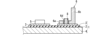
- FIG. 1 is a schematic cross-sectional view of a joint portion 6a of an electrode terminal 6 and its surroundings included in the semiconductor device according to the first embodiment.
- the semiconductor device includes an insulating substrate 1, a semiconductor element 5, and an electrode terminal 6.
- the insulating substrate 1 includes an insulating layer 2, a circuit pattern 3, and a base plate 4.
- the insulating layer 2 is made of ceramic or the like.
- a plurality of conductive circuit patterns 3 are provided on the upper surface of the insulating layer 2 .
- the circuit pattern 3 is made of, for example, Cu.
- a base plate 4 is provided on the lower surface of the insulating layer 2.
- An electrode terminal 6 is bonded to the upper surface of the circuit pattern 3 using a bonding material 7. Further, on the upper surface of the circuit pattern 3 adjacent to the circuit pattern 3 to which the electrode terminal 6 is bonded, a plurality of semiconductor elements 5 such as IGBT (Insulated Gate Bipolar Transistor) and FWDI (Free Wheeling Diode) are soldered (not shown). It is joined by Adjacent circuit patterns 3 are connected by aluminum wires (not shown). Further, the insulating substrate 1, the semiconductor element 5, and the electrode terminal 6 are protected by a case (not shown) and a sealing material such as gel (not shown). Note that, as the semiconductor element 5, a MOSFET (Metal Oxide Semiconductor Field Effect Transistor) may be mounted instead of the IGBT. Further, instead of FWDI, an SBD (Schottky diode) may be installed.
- IGBT Insulated Gate Bipolar Transistor
- FWDI Free Wheeling Diode
- the electrode terminal 6 is electrically connected to the semiconductor element 5 via an aluminum wire (not shown).
- the electrode terminal 6 is made of Al, for example.
- the electrode terminal 6 includes a joint portion 6a provided at one end of the electrode terminal 6, and a bent portion 6b bent upward from the joint portion 6a.
- the bonding portion 6a is a portion that extends parallel to the top surface of the circuit pattern 3 and is a portion that is bonded to the top surface of the circuit pattern 3.
- the lower surface of the joint portion 6a is flat and in contact with the circuit pattern 3 over the entire surface.
- the joint portion 6a is provided with a sagging surface 6c that protrudes downward from the outer peripheral surface.
- the sagging surface 6c is provided over a part or the entire circumference of the outer peripheral surface of the joint portion 6a of the electrode terminal 6.
- the sagging surface 6c is provided only on a part of the outer peripheral surface of the joint portion 6a, it is preferably provided on the tip side of the joint portion 6a.
- the distal end side of the joint portion 6a is the left side in FIG. 1, that is, the side opposite to the bent portion 6b.
- a recess 3a that can fit with the sagging surface 6c is provided on the upper surface of the circuit pattern 3 at the portion to be joined to the electrode terminal 6. Specifically, the tip of the sagging surface 6c is fitted into the recess 3a.
- the recess 3a is provided at a position facing the sagging surface 6c on the upper surface of the circuit pattern 3, and is formed in a size that allows it to fit into the tip of the sagging surface 6c.
- the electrode terminal 6 is positioned on the circuit pattern 3 by fitting the sagging surface 6c into the recess 3a.
- the recess 3a corresponds to a fitting part
- the sagging surface 6c corresponds to a fitted part.
- the bonding material 7 is arranged to cover the bonding portion 6a of the electrode terminal 6 and a portion of the bent portion 6b.
- the bonding material 7 is, for example, solder.
- a method for forming the sagging surface 6c which is included in the method for manufacturing a semiconductor device, will be briefly explained without using drawings.
- a metal plate that will become the electrode terminal 6 is placed in a lower mold.
- the metal plate is punched out with a gap left between the lower die and the opposing upper die.
- the electrode terminal 6 having the sagging surface 6c is manufactured.
- the electrode terminal 6 is manufactured by minimizing the gap between the upper mold and the lower mold to prevent the formation of the sagging surface 6c.
- the electrode terminal 6 having the sagging surface 6c is manufactured by widening the gap between the electrode terminal 6 and the sagging surface 6c.
- the semiconductor device includes the insulating substrate 1 on which the circuit pattern 3 is formed, and the electrode terminal 6 having the bonding portion 6a to be bonded to the top surface of the circuit pattern 3.
- the circuit pattern 3 is provided with a fitting portion
- the joint portion 6a of the electrode terminal 6 is provided with a fitted portion that is fitted with the sagging surface 6c.
- the fitting portion is a recess 3a provided in the circuit pattern 3
- the fitted portion is a sagging surface 6c protruding downward from the outer peripheral surface of the joint portion 6a of the electrode terminal 6.
- the electrode terminal 6 is positioned on the circuit pattern 3 by fitting the surface 6c into the recess 3a.
- the sagging surface 6c on the electrode terminal 6 it becomes easier to form a solder fillet. As described above, the yield of the semiconductor device is improved and the durability is improved.
- a metal plate serving as the electrode terminal 6 is placed in a lower mold, and the metal plate is punched out with a gap left between the lower mold and an upper mold opposing thereto.
- the metal plate is plastically deformed to form the sagging surface 6c. Therefore, since the sagging surface 6c can be formed in the punching process for producing the electrode terminal 6, an increase in the number of manufacturing processes can be suppressed.
- FIG. 2 is a schematic cross-sectional view of the joint portion 6a of the electrode terminal 6 and its surroundings included in the semiconductor device according to the second embodiment. Note that, in the second embodiment, the same components as those described in the first embodiment are given the same reference numerals, and a description thereof will be omitted.
- the entire lower end portion of the joint portion 6a functions as a fitted portion without providing the sagging surface 6c (see FIG. 1) on the joint portion 6a of the electrode terminal 6. There is.
- the recess 3a provided in the circuit pattern 3 is formed in a size that allows the entire lower end portion of the joint portion 6a to fit therein. Further, the maximum depth of the recess 3a is less than or equal to 1/2 of the thickness of the circuit pattern 3. More preferably, the maximum depth of the recess 3a is 1/4 or more and 1/2 or less of the thickness of the circuit pattern 3.
- the fitting portion is the recess 3a provided in the circuit pattern 3, and the maximum depth of the recess 3a is 1/2 or less of the thickness of the circuit pattern 3.
- the fitted part is the lower end of the joint part 6a of the electrode terminal 6, and the lower end of the joint part 6a of the electrode terminal 6 is fitted into the recess 3a, so that the electrode terminal 6 is connected to the circuit pattern 3.
- the electrode terminal 6 is mounted on the circuit pattern 3 of the insulating substrate 1 by fitting the lower end portion of the joint portion 6a as the fitting portion of the electrode terminal 6 into the recess 3a as the fitting portion of the circuit pattern 3. It is possible to suppress positional deviation when Thereby, it is also possible to suppress misalignment between the circuit pattern 3 and the electrode terminal 6 when they are bonded.
- the thermal resistance from the electrode terminals 6 to the radiation fins (not shown) attached to the lower surface of the base plate 4 is reduced. This makes it easier to radiate heat generated at the electrode terminal 6 from the radiation fins.
- FIG. 3 is a schematic cross-sectional view of the joint portion 6a of the electrode terminal 6 and its surroundings before caulking, which is included in the semiconductor device according to the third embodiment.
- FIG. 4 is a schematic cross-sectional view of the joint portion 6a of the electrode terminal 6 and its surroundings after caulking, which is included in the semiconductor device according to the third embodiment.
- the same components as those explained in the first and second embodiments are designated by the same reference numerals, and the explanation thereof will be omitted.
- a projection 8 that projects upward is provided on the upper surface of the circuit pattern 3.
- the protrusion 8 is formed in a columnar or cylindrical shape, and is formed integrally with the circuit pattern 3.
- the vertical length of the protrusion 8 is longer than the thickness of the joint portion 6a of the electrode terminal 6.
- the joint portion 6a of the electrode terminal 6 is provided with a through hole 6d into which the protrusion 8 can fit.
- the diameter of the through hole 6d is made slightly larger than the diameter of the protrusion 8 in order to allow the protrusion 8 to deform when the tip of the protrusion 8 is caulked.
- the electrode terminal 6 is positioned on the circuit pattern 3 by fitting the through hole 6d into the protrusion 8. After positioning, as shown in FIG. 4, the tip of the protrusion 8 is caulked so as to fit into the through hole 6d. Thereby, the electrode terminal 6 and the circuit pattern 3 are bonded without using the bonding material 7 (see FIG. 1).
- the protrusion 8 corresponds to a fitting part
- the through hole 6d corresponds to a fitted part.
- the electrode terminal 6 is placed on the circuit pattern 3 so that the through hole 6d of the joint portion 6a fits into the protrusion 8 of the circuit pattern 3.
- a load is applied to the tip of the protrusion 8 using an ultrasonic bonding tool (not shown). As a result, as shown in FIG. 4, the tip of the protrusion 8 is caulked.
- the fitting portion is the protrusion 8 provided on the circuit pattern 3, and the fitting portion is the through hole provided on the joint portion 6a of the electrode terminal 6.
- the electrode terminal 6 is positioned on the circuit pattern 3 by fitting the protrusion 8 into the through hole 6d.
- the electrode terminal 6 is attached to the circuit pattern 3 of the insulating substrate 1. It is possible to suppress positional deviation when mounted. Thereby, it is also possible to suppress misalignment between the circuit pattern 3 and the electrode terminal 6 when they are bonded.
- the circuit pattern 3 and the electrode terminal 6 can be bonded without using the bonding material 7.
- the protrusion 8 is integrated with the circuit pattern 3, there is no need to bond the protrusion 8 and the circuit pattern 3, which further improves the reliability of the bond between the electrode terminal 6 and the circuit pattern 3. .
- the protrusion 8 is formed in a cylindrical or cylindrical shape, uniform deformation of the protrusion 8 allows for close contact with the through hole 6d. This further strengthens the bond between the circuit pattern 3 and the electrode terminal 6.
Landscapes
- Wire Bonding (AREA)
- Structures For Mounting Electric Components On Printed Circuit Boards (AREA)
Priority Applications (5)
| Application Number | Priority Date | Filing Date | Title |
|---|---|---|---|
| PCT/JP2022/031026 WO2024038511A1 (ja) | 2022-08-17 | 2022-08-17 | 半導体装置および半導体装置の製造方法 |
| CN202280096070.4A CN119631174A (zh) | 2022-08-17 | 2022-08-17 | 半导体装置及半导体装置的制造方法 |
| US18/860,788 US20250300045A1 (en) | 2022-08-17 | 2022-08-17 | Semiconductor device and method for manufacturing semiconductor device |
| DE112022007665.8T DE112022007665T5 (de) | 2022-08-17 | 2022-08-17 | Halbleitervorrichtung und Verfahren zur Herstellung einer Halbleitervorrichtung |
| JP2024541320A JP7690133B2 (ja) | 2022-08-17 | 2022-08-17 | 半導体装置および半導体装置の製造方法 |
Applications Claiming Priority (1)
| Application Number | Priority Date | Filing Date | Title |
|---|---|---|---|
| PCT/JP2022/031026 WO2024038511A1 (ja) | 2022-08-17 | 2022-08-17 | 半導体装置および半導体装置の製造方法 |
Publications (1)
| Publication Number | Publication Date |
|---|---|
| WO2024038511A1 true WO2024038511A1 (ja) | 2024-02-22 |
Family
ID=89941531
Family Applications (1)
| Application Number | Title | Priority Date | Filing Date |
|---|---|---|---|
| PCT/JP2022/031026 Ceased WO2024038511A1 (ja) | 2022-08-17 | 2022-08-17 | 半導体装置および半導体装置の製造方法 |
Country Status (5)
| Country | Link |
|---|---|
| US (1) | US20250300045A1 (https=) |
| JP (1) | JP7690133B2 (https=) |
| CN (1) | CN119631174A (https=) |
| DE (1) | DE112022007665T5 (https=) |
| WO (1) | WO2024038511A1 (https=) |
Citations (5)
| Publication number | Priority date | Publication date | Assignee | Title |
|---|---|---|---|---|
| JPH0567871A (ja) * | 1991-04-26 | 1993-03-19 | Nec Toyama Ltd | 印刷配線板及びその製造方法 |
| JPH09283901A (ja) * | 1996-04-12 | 1997-10-31 | Nec Corp | 表面実装lsiパッケージの実装方法および構造 |
| JP2017069521A (ja) * | 2015-10-02 | 2017-04-06 | 株式会社日立製作所 | 半導体パワーモジュールおよび移動体 |
| JP2020178003A (ja) * | 2019-04-17 | 2020-10-29 | 三菱電機株式会社 | パワー半導体モジュールおよびパワー半導体モジュールの製造方法 |
| WO2022018868A1 (ja) * | 2020-07-22 | 2022-01-27 | 三菱電機株式会社 | 半導体装置、電力変換装置、移動体、および半導体装置の製造方法 |
-
2022
- 2022-08-17 CN CN202280096070.4A patent/CN119631174A/zh active Pending
- 2022-08-17 WO PCT/JP2022/031026 patent/WO2024038511A1/ja not_active Ceased
- 2022-08-17 US US18/860,788 patent/US20250300045A1/en active Pending
- 2022-08-17 DE DE112022007665.8T patent/DE112022007665T5/de active Pending
- 2022-08-17 JP JP2024541320A patent/JP7690133B2/ja active Active
Patent Citations (5)
| Publication number | Priority date | Publication date | Assignee | Title |
|---|---|---|---|---|
| JPH0567871A (ja) * | 1991-04-26 | 1993-03-19 | Nec Toyama Ltd | 印刷配線板及びその製造方法 |
| JPH09283901A (ja) * | 1996-04-12 | 1997-10-31 | Nec Corp | 表面実装lsiパッケージの実装方法および構造 |
| JP2017069521A (ja) * | 2015-10-02 | 2017-04-06 | 株式会社日立製作所 | 半導体パワーモジュールおよび移動体 |
| JP2020178003A (ja) * | 2019-04-17 | 2020-10-29 | 三菱電機株式会社 | パワー半導体モジュールおよびパワー半導体モジュールの製造方法 |
| WO2022018868A1 (ja) * | 2020-07-22 | 2022-01-27 | 三菱電機株式会社 | 半導体装置、電力変換装置、移動体、および半導体装置の製造方法 |
Also Published As
| Publication number | Publication date |
|---|---|
| DE112022007665T5 (de) | 2025-06-12 |
| JP7690133B2 (ja) | 2025-06-09 |
| US20250300045A1 (en) | 2025-09-25 |
| CN119631174A (zh) | 2025-03-14 |
| JPWO2024038511A1 (https=) | 2024-02-22 |
Similar Documents
| Publication | Publication Date | Title |
|---|---|---|
| JP4453498B2 (ja) | パワー半導体モジュールおよびその製造方法 | |
| US10104775B2 (en) | Semiconductor device and method for manufacturing the same | |
| EP3226292B1 (en) | Lead frame, semiconductor device, method for manufacturing lead frame, and method for manufacturing semiconductor device | |
| EP3544053B1 (en) | Discrete power transistor package having solderless dbc to leadframe attach | |
| US8981552B2 (en) | Power converter, semiconductor device, and method for manufacturing power converter | |
| CN112750801B (zh) | 功率半导体装置 | |
| JPWO2018179981A1 (ja) | 半導体装置 | |
| CN113097173B (zh) | 半导体封装及其制造方法 | |
| CN111386603B (zh) | 半导体装置的制造方法和半导体装置 | |
| JP7233604B2 (ja) | 半導体装置およびその製造方法 | |
| JP2009224560A (ja) | 半導体装置およびその製造方法 | |
| JP4899481B2 (ja) | 外部に露出する放熱体を上部に有する樹脂封止型半導体装置の製法 | |
| JP5898575B2 (ja) | 半導体装置 | |
| JPH09232341A (ja) | 半導体装置 | |
| KR20150129269A (ko) | 반도체 패키지를 위한 클립 구조체 및 이를 이용한 반도체 패키지, 제조 방법 | |
| JP2009164240A (ja) | 半導体装置 | |
| JP7690133B2 (ja) | 半導体装置および半導体装置の製造方法 | |
| JP4769965B2 (ja) | 半導体装置およびその製造方法 | |
| JP7322369B2 (ja) | 半導体装置の製造方法 | |
| JP5342596B2 (ja) | 半導体装置およびその製造方法 | |
| JP4861200B2 (ja) | パワーモジュール | |
| JP2009164511A (ja) | 半導体装置およびその製造方法 | |
| JP2022165097A (ja) | 半導体装置および半導体装置の製造方法 | |
| JP7822489B2 (ja) | 半導体装置 | |
| JP2002076259A (ja) | パワーモジュール |
Legal Events
| Date | Code | Title | Description |
|---|---|---|---|
| 121 | Ep: the epo has been informed by wipo that ep was designated in this application |
Ref document number: 22955685 Country of ref document: EP Kind code of ref document: A1 |
|
| ENP | Entry into the national phase |
Ref document number: 2024541320 Country of ref document: JP Kind code of ref document: A |
|
| WWE | Wipo information: entry into national phase |
Ref document number: 18860788 Country of ref document: US |
|
| WWE | Wipo information: entry into national phase |
Ref document number: 202280096070.4 Country of ref document: CN |
|
| WWP | Wipo information: published in national office |
Ref document number: 202280096070.4 Country of ref document: CN |
|
| WWE | Wipo information: entry into national phase |
Ref document number: 112022007665 Country of ref document: DE |
|
| WWP | Wipo information: published in national office |
Ref document number: 112022007665 Country of ref document: DE |
|
| 122 | Ep: pct application non-entry in european phase |
Ref document number: 22955685 Country of ref document: EP Kind code of ref document: A1 |
|
| WWP | Wipo information: published in national office |
Ref document number: 18860788 Country of ref document: US |