WO2024029286A1 - 半導体装置、および、半導体装置の製造方法 - Google Patents
半導体装置、および、半導体装置の製造方法 Download PDFInfo
- Publication number
- WO2024029286A1 WO2024029286A1 PCT/JP2023/025566 JP2023025566W WO2024029286A1 WO 2024029286 A1 WO2024029286 A1 WO 2024029286A1 JP 2023025566 W JP2023025566 W JP 2023025566W WO 2024029286 A1 WO2024029286 A1 WO 2024029286A1
- Authority
- WO
- WIPO (PCT)
- Prior art keywords
- wire
- semiconductor device
- electrode
- buffer
- terminal
- Prior art date
- Legal status (The legal status is an assumption and is not a legal conclusion. Google has not performed a legal analysis and makes no representation as to the accuracy of the status listed.)
- Ceased
Links
Images


Classifications
-
- H—ELECTRICITY
- H10—SEMICONDUCTOR DEVICES; ELECTRIC SOLID-STATE DEVICES NOT OTHERWISE PROVIDED FOR
- H10W—GENERIC PACKAGES, INTERCONNECTIONS, CONNECTORS OR OTHER CONSTRUCTIONAL DETAILS OF DEVICES COVERED BY CLASS H10
- H10W72/00—Interconnections or connectors in packages
- H10W72/071—Connecting or disconnecting
Definitions
- the present disclosure relates to a semiconductor device and a method for manufacturing a semiconductor device.
- Patent Document 1 discloses a semiconductor device that is a power module.
- the semiconductor device includes a substrate on which a mounting layer and a conductive layer are arranged, a plurality of switching elements, and a plurality of wires.
- the plurality of switching elements are electrically connected to the mounting layer.
- Each of the plurality of wires connects the main surface electrode of the switching element to the conductive layer.
- the constituent material of the plurality of wires is aluminum.
- An object of the present disclosure is to provide a semiconductor device that is improved over the conventional semiconductor device. Particularly, in view of the above-mentioned circumstances, one object of the present disclosure is to provide a semiconductor device that can alleviate the impact applied to a semiconductor element during wire bonding and can suppress an increase in manufacturing costs.
- a semiconductor device provided by a first aspect of the present disclosure includes a semiconductor element having an element main surface and an element back surface facing opposite to each other in the thickness direction, and a first electrode disposed on the element main surface. , a buffer part electrically connected to the first electrode, and a first wire electrically connected to the buffer part and containing a first metal.
- a method for manufacturing a semiconductor device provided by a second aspect of the present disclosure includes a buffer portion forming step of forming a buffer portion by bonding and cutting a wire material to a first electrode of a semiconductor element; and a first wire bonding step of bonding a first wire to the portion.
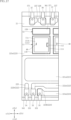
- FIG. 1 is a perspective view showing a semiconductor device according to a first embodiment of the present disclosure.
- FIG. 2 is a plan view of the semiconductor device shown in FIG. 1, and is a view through a resin member.
- FIG. 3 is a partially enlarged view of FIG. 2.
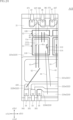
- FIG. 4 is a cross-sectional view taken along line IV-IV in FIG. 2.
- FIG. 5 is a sectional view taken along line VV in FIG. 2.
- FIG. 6 is a cross-sectional view taken along line VI-VI in FIG.
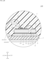
- FIG. 7 is a cross-sectional view taken along line VII-VII in FIG. 6.
- FIG. 8 is a perspective view showing a state in which a driving device is attached to the semiconductor device shown in FIG. FIG.
- FIG. 9 is a circuit diagram showing an example of the circuit configuration of the semiconductor device shown in FIG. 1.
- FIG. 10 is a flowchart showing an example of a method for manufacturing the semiconductor device shown in FIG.
- FIG. 11 is a cross-sectional view showing steps in an example of the method for manufacturing the semiconductor device shown in FIG.
- FIG. 12 is a cross-sectional view showing steps in an example of the method for manufacturing the semiconductor device shown in FIG.
- FIG. 13 is a cross-sectional view showing steps in an example of the method for manufacturing the semiconductor device shown in FIG.
- FIG. 14 is a cross-sectional view showing steps in an example of the method for manufacturing the semiconductor device shown in FIG.
- FIG. 15 is a front view showing the entire wedge tool.
- FIG. 16 is a cross-sectional view of the wedge tool shown in FIG.
- FIG. 17 is a partially enlarged plan view showing steps in an example of the method for manufacturing the semiconductor device shown in FIG.
- FIG. 18 is a cross-sectional view showing steps in an example of the method for manufacturing the semiconductor device shown in FIG.
- FIG. 19 is a cross-sectional view showing steps in an example of the method for manufacturing the semiconductor device shown in FIG.
- FIG. 20 is a cross-sectional view showing steps in an example of the method for manufacturing the semiconductor device shown in FIG.
- FIG. 21 is a front view showing steps in an example of the method for manufacturing the semiconductor device shown in FIG. 1.
- FIG. 22 is a partially enlarged sectional view showing a semiconductor device according to a first modification of the first embodiment.
- FIG. 22 is a partially enlarged sectional view showing a semiconductor device according to a first modification of the first embodiment.
- FIG. 23 is a partially enlarged plan view showing a semiconductor device according to a second modification of the first embodiment.
- FIG. 24 is a partially enlarged plan view showing a semiconductor device according to a third modification of the first embodiment.
- FIG. 25 is a partially enlarged plan view showing a semiconductor device according to a fourth modification of the first embodiment.
- FIG. 26 is a partially enlarged plan view showing a semiconductor device according to a second embodiment of the present disclosure.
- FIG. 27 is a cross-sectional view taken along line XXVII-XXVII in FIG. 26.
- FIG. 28 is a partially enlarged sectional view showing a semiconductor device according to a third embodiment of the present disclosure.
- FIG. 29 is a plan view showing a semiconductor device according to a fourth embodiment of the present disclosure, and is a view through a resin member.
- the semiconductor device A10 includes a plurality of semiconductor elements 11, a plurality of semiconductor elements 12, a support member 2, a plurality of terminals 3, a plurality of wires 41 to 47, a buffer section 48, and a resin member 5.
- the plurality of terminals 3 include power terminals 31 and 32, signal terminals 33, detection terminals 34 and 35, and temperature detection terminals 36 and 37.
- the semiconductor device A10 is used with the drive device 7 attached.
- FIG. 1 is a perspective view showing the semiconductor device A10.
- FIG. 2 is a plan view of the semiconductor device A10.
- the outer shape of the resin member 5 is shown by an imaginary line (two-dot chain line) that is transmitted through the resin member 5.
- FIG. 3 is a partially enlarged view of FIG. 2.
- FIG. 4 is a cross-sectional view taken along line IV-IV in FIG. 2.
- FIG. 5 is a sectional view taken along line VV in FIG. 2. Note that the plurality of wires 41 to 47 are omitted in FIGS. 4 and 5.
- FIG. 6 is a cross-sectional view taken along line VI-VI in FIG.
- FIG. 7 is a cross-sectional view taken along line VII-VII in FIG. 6.
- FIG. 8 is a perspective view showing a state in which the driving device 7 is attached to the semiconductor device A10.
- FIG. 9 is a circuit diagram showing an example of the circuit configuration of the semiconductor device A10.
- the shape of the portion of the semiconductor device A10 covered with the resin member 5 when viewed in the thickness direction is rectangular.
- the thickness direction (planar view direction) of the semiconductor device A10 is defined as the z direction
- the direction in which the power terminals 31 and 32 of the semiconductor device A10 protrude perpendicularly to the z direction is defined as the x direction.
- the direction perpendicular to the z-direction and the x-direction (the vertical direction in FIG. 2) is defined as the y-direction.
- one side in the z direction (the lower side in FIGS. 4 and 5) is the z1 side
- the other side is the z2 side.
- One side in the x direction (the left side in FIG. 2) is the x1 side, and the other side (the right side in FIG. 2) is the x2 side.
- One side in the y direction (the lower side in FIG. 2) is the y1 side, and the other side (the upper side in FIG. 2) is the y2 side.
- the z direction corresponds to the "thickness direction" of the present disclosure.
- Each dimension of the semiconductor device A10 is not particularly limited.
- the plurality of semiconductor elements 11 are elements that perform the electrical functions of the semiconductor device A10.
- Each semiconductor element 11 is constructed using a semiconductor material mainly composed of SiC (silicon carbide), for example. Note that the semiconductor material is not limited to SiC, and may be Si (silicon), GaAs (gallium arsenide), GaN (gallium nitride), or the like.
- Each semiconductor element 11 is a switching element such as a MOSFET (Metal-Oxide-Semiconductor Field-Effect Transistor).
- each semiconductor element 11 is not limited to a MOSFET, and may be a field effect transistor including a MISFET (Metal-Insulator-Semiconductor FET), or a bipolar transistor such as an IGBT (Insulated Gate Bipolar Transistor).
- the plurality of semiconductor elements 11 are each an n-channel MOSFET, for example, and are all the same element. Note that each semiconductor element 11 may be a p-channel type MOSFET.
- the plurality of semiconductor elements 11 are arranged at equal intervals in the x direction and connected in parallel to each other.
- the semiconductor device A10 includes five semiconductor elements 11. Note that the number of semiconductor elements 11 is not limited to this, and can be freely set according to the performance required of the semiconductor device A10.
- Each semiconductor element 11 is bonded onto the support member 2 using a conductive bonding material 110.
- the conductive bonding material 110 is, for example, solder, silver paste, or sintered metal.
- Each semiconductor element 11 has an element main surface 11a and an element back surface 11b.
- the element main surface 1 1a and the element back surface 11b face opposite to each other in the z direction.
- the element main surface 11a faces the z2 side in the z direction.
- the back surface 11b of the element faces the z1 side in the z direction.
- the element back surface 11b faces the support member 2.
- each semiconductor element 11 has a first electrode 111, a second electrode 112, and a third electrode 113.
- the first electrode 111 and the second electrode 112 are arranged on the element main surface 11a.
- the first electrode 111 is larger than the second electrode 112 in plan view.
- the third electrode 113 is arranged on the back surface 12b of the element.
- the third electrode 113 covers substantially the entire surface of the back surface 11b of the element.
- the first electrode 111 includes a first metal layer 111a and a second metal layer 111b.
- the constituent material of the first metal layer 111a is not limited, it is Al in this embodiment.
- the second metal layer 111b is formed on the first metal layer 111a by, for example, plating.
- the second metal layer 111b may be formed by other processing.
- the constituent material of the second metal layer 111b is not limited, it is Cu in this embodiment.
- the thickness dimension (dimension in the z direction) of the second metal layer 111b is 50 ⁇ m or less.
- another conductive layer may be interposed between the first metal layer 111a and the second metal layer 111b.
- the constituent material of the second electrode 112 and the third electrode 113 is not limited, it is Al in this embodiment.
- the first electrode 111 is a source electrode
- the second electrode 112 is a gate electrode
- the third electrode 113 is a drain electrode.
- the third electrode 113 is conductively bonded to a part of the support member 2 (the conductor layer 223 of the main surface metal layer 22, which will be described later) via the conductive bonding material 110.
- the third electrode 113 is in contact with the conductive bonding material 110.
- Wires 41, 44 to 46 and a buffer section 48 are connected to the first electrode 111.
- a wire 43 is connected to the second electrode 112.
- the plurality of semiconductor elements 12 are, for example, diodes such as Schottky barrier diodes. Each semiconductor element 12 is connected in antiparallel to each semiconductor element 11, as shown in FIG.
- Each semiconductor element 12 is bonded onto the support member 2 with a conductive bonding material 120.
- the conductive bonding material 120 is, for example, solder, silver paste, or sintered metal.
- the number of semiconductor elements 12 corresponds to the number of semiconductor elements 11. Note that the semiconductor device A10 does not need to include each semiconductor element 12.
- Each semiconductor element 12 has an element main surface 12a and an element back surface 12b.
- the element main surface 12a and the element back surface 12b face opposite to each other in the z direction.
- the element main surface 12a faces the z2 side in the z direction.
- the element back surface 12b faces the z1 side in the z direction.
- the element back surface 12b faces the support member 2.
- Each semiconductor element 12 has an anode electrode 121 and a cathode electrode 122.
- the anode electrode 121 is arranged on the element main surface 12a.
- the cathode electrode 122 is arranged on the back surface 12b of the element.
- the cathode electrode 122 is electrically connected to a part of the support member 2 (the conductor layer 223 of the main surface metal layer 22, which will be described later), via the conductive bonding material 120.
- Cathode electrode 122 is in contact with conductive bonding material 120 .
- the support member 2 is a member that supports the plurality of semiconductor elements 11 and 12, respectively, and forms a conduction path between each semiconductor element 11 and the plurality of terminals 3.
- the support member 2 includes an insulating substrate 21 , a main surface metal layer 22 , and a back surface metal layer 23 .
- the insulating substrate 21 has, for example, a flat plate shape and has electrical insulation properties.
- the constituent material of the insulating substrate 21 is, for example, ceramics with excellent thermal conductivity, and in this embodiment, it is Al 2 O 3 (aluminum oxide).
- the constituent material of the insulating substrate 21 is not limited, and may be other ceramics such as AlN (aluminum nitride) and SiN (silicon nitride).
- the constituent material of the insulating substrate 21 is not limited to ceramics, and may be Si or synthetic resin.
- the constituent material of the insulating substrate 21 may be any material as long as it has insulating properties and can withstand the heat generated by the semiconductor element 11.
- the insulating substrate 21 has a main surface 211 and a back surface 212.
- the main surface 211 and the back surface 212 face opposite to each other in the z direction.
- the main surface 211 faces the z2 side in the z direction.
- the back surface 212 faces the z1 side in the z direction.
- the main surface metal layer 22 is formed on the main surface 211 of the insulating substrate 21.
- the constituent material of the main surface metal layer 22 is, for example, a metal containing Cu. Note that the constituent material of the main surface metal layer 22 is not limited.
- the main surface metal layer 22 is formed, for example, by plating. Note that the method for forming the main surface metal layer 22 is not limited.
- the main surface metal layer 22 is covered with a resin member 5.
- the main surface metal layer 22 includes conductor layers 221 to 225 and a plurality of conductor layers 226 and 227, respectively. The conductive layers 221 to 227 are spaced apart from each other.
- the conductor layer 221 includes a strip portion 221a and a terminal joint portion 221b.
- the strip portion 221a extends along the x direction, and a plurality of wires 41 and wires 42 are respectively bonded to the strip portion 221a.
- the terminal joint portion 221b is connected to the end portion of the strip portion 221a on the x2 side in the x direction, and a portion of the power terminal 32 (pad portion 321, which will be described later) is joined to the terminal joint portion 221b.
- the conductor layer 222 includes a strip portion 222a and a terminal joint portion 222b.
- the strip portion 222a extends along the x direction, and a plurality of wires 43 are respectively bonded to the strip portion 222a.
- the terminal joint portion 222b is connected to the end of the strip portion 222a on the x1 side in the x direction, and a portion of the signal terminal 33 (pad portion 331 to be described later) is joined to the terminal joint portion 222b.
- the conductor layer 223 includes a strip portion 223a and a terminal joint portion 223b.
- the strip portion 223a extends along the x direction, and a plurality of semiconductor elements 11 and 12 are bonded to each strip portion 223a. Heat from each semiconductor element 11 is appropriately transmitted to the strip portion 223a (conductor layer 223) via the conductive bonding material 110.
- the plurality of semiconductor elements 11 bonded to the strip portion 223a are arranged in the direction in which the strip portion 223a extends (x direction).
- the terminal joint portion 223b is connected to the end portion of the strip portion 223a on the x1 side in the x direction, and a portion of the power terminal 31 (pad portion 311 to be described later) is joined to the terminal joint portion 223b.
- the conductor layer 223 is electrically connected to the third electrode 113 (drain electrode) of each semiconductor element 11 via each conductive bonding material 110, and is electrically connected to each conductive bonding material 120. It is electrically connected to the cathode electrode 122 of each semiconductor element 12 via. That is, the third electrode 113 of each semiconductor element 11 and the cathode electrode 122 of each semiconductor element 12 are electrically connected via the conductor layer 223.
- the conductor layer 224 includes a strip portion 224a and a terminal joint portion 224b.
- the strip portion 224a extends along the x direction, and a plurality of wires 44 are respectively bonded to the strip portion 224a.
- the terminal joint portion 224b is connected to the end of the strip portion 224a on the x1 side in the x direction, and a portion of the detection terminal 35 (pad portion 351, which will be described later) is joined to the terminal joint portion 224b.
- the wire 42 is bonded to the conductive layer 225. Further, a portion of the detection terminal 34 (pad portion 341 described later) is bonded to the conductor layer 225.
- the plurality of strips 221a, 222a, 223a, and 224a are lined up in the y direction and overlap each other when viewed in the y direction.
- the arrangement of the plurality of strips 221a, 222a, 223a, and 224a in the y direction is not particularly limited.
- the strip portion 224a, the strip portion 222a, the strip portion 221a, and the strip portion 223a are arranged in this order from the y-direction y1 side to the y-direction y2 side.
- the strip portion 221a is arranged between the strip portion 222a and the strip portion 223a in the y direction, and the strip portion 222a is arranged between the strip portion 221a and the strip portion 224a in the y direction.
- the strip portion 223a is arranged on the opposite side of the strip portion 222a with the strip portion 221a interposed therebetween in the y direction.
- the conductor layer 225 is arranged on the x1 side of the terminal joint portion 222b of the conductor layer 222 in the x direction.
- Each of the plurality of conductor layers 226 and 227 is arranged on the y-direction y2 side of the strip portion 223a of the conductor layer 223.
- the main surface metal layer 22 includes the same number of conductor layers 226 and conductor layers 227 as the semiconductor element 11 (five in this embodiment).
- the conductor layers 226 and 227 are alternately arranged along the x direction.
- a wire 46 is bonded to each conductor layer 226 . Further, each conductor layer 226 is connected to a portion of the temperature detection terminal 36 (pad portion 361 described later).
- a wire 47 is connected to each conductor layer 227 . Further, each conductor layer 227 is connected to a portion of the temperature detection terminal 37 (pad portion 371 described later).
- each of the conductor layers 221 to 227 are not limited to those described above, and are appropriately designed depending on the arrangement position of each terminal 3 and the like.
- the back metal layer 23 is formed on the back surface 212 of the insulating substrate 21.
- the constituent material of the back metal layer 23 is, for example, a metal containing Cu. Note that the constituent material is not limited.
- the back metal layer 23 is formed, for example, by electroless plating. Note that the method for forming the back metal layer 23 is not limited. As shown in FIGS. 4 and 5, the surface of the back metal layer 23 facing the z1 side in the z direction is exposed from the resin member 5. Note that the surface facing the z-direction z1 side may be covered with the resin member 5. Further, the support member 2 does not need to include the back metal layer 23. In this case, the back surface 212 of the insulating substrate 21 may be covered with the resin member 5 or may be exposed from the resin member 5.
- Each terminal 3 is joined to the main surface metal layer 22 inside the resin member 5. Each terminal 3 protrudes from the insulating substrate 21 when viewed in the z direction. Further, each terminal 3 is partially exposed from the resin member 5. Each terminal 3 is composed of, for example, the same lead frame. Each terminal 3 is made of metal, preferably Cu or Ni, or an alloy thereof, a 42 alloy, or the like.
- the power terminal 31 is a drain terminal in the semiconductor device A10.
- the power terminal 31 is a plate-shaped member.
- the power terminal 31 is electrically connected to the third electrode 113 (drain electrode) of each semiconductor element 11 via the conductor layer 223 and the conductive bonding material 110.
- the power terminal 31 includes a pad portion 311 and a terminal portion 312.
- the pad portion 311 is covered with the resin member 5.
- the pad portion 311 is bonded to the conductor layer 223. This joining may be performed by any method such as joining using a conductive joining material (solder, silver paste, sintered metal, etc.), laser joining, or ultrasonic joining.
- the terminal portion 312 is exposed from the resin member 5. As shown in FIG. 2, the terminal portion 312 extends from the resin member 5 toward the x1 side in the x direction when viewed in the z direction. Note that the surface of the terminal portion 312 may be plated with silver, for example.
- the power terminal 32 is a source terminal in the semiconductor device A10.
- the power terminal 32 is a plate-shaped member.
- the power terminal 32 is electrically connected to the first electrode 111 (source electrode) of each semiconductor element 11 via the conductor layer 221 and the plurality of wires 41.
- the power terminal 32 includes a pad portion 321 and a terminal portion 322.
- the pad portion 321 is covered with the resin member 5.
- the pad portion 321 is bonded to the conductive layer 221. This bonding may be performed by any method such as bonding using a conductive bonding material, laser bonding, or ultrasonic bonding.
- the terminal portion 322 is exposed from the resin member 5. As shown in FIG. 2, the terminal portion 322 extends from the resin member 5 toward the x2 side in the x direction when viewed in the z direction. Note that the surface of the terminal portion 322 may be plated with silver, for example.
- the signal terminal 33 is a gate terminal in the semiconductor device A10.
- the signal terminal 33 is electrically connected to the second electrode 112 (gate electrode) of each semiconductor element 11 via the conductor layer 222 and the plurality of wires 43.
- a drive signal for controlling on/off of each semiconductor element 11 is input to the signal terminal 33 .
- a drive circuit DR is connected to the signal terminal 33, as shown in FIG.
- the drive circuit DR generates a drive signal that controls the switching operation of each semiconductor element 11.
- a drive signal is input to the signal terminal 33 from the drive circuit DR.
- the drive circuit DR shown in FIG. 9 is an example, and the drive circuit DR is not limited to the illustrated circuit configuration.
- the signal terminal 33 includes a pad portion 331 and a terminal portion 332.
- the pad portion 331 is covered with the resin member 5.
- Pad portion 331 is bonded to conductor layer 222 . This bonding may be performed by any method such as bonding using a conductive bonding material, laser bonding, or ultrasonic bonding.
- the terminal portion 332 is exposed from the resin member 5.
- the terminal portion 332 is L-shaped when viewed in the x direction.
- the detection terminal 34 is a source sense terminal in the semiconductor device A10.
- the detection terminal 34 is electrically connected to the first electrode 111 (source electrode) of the semiconductor element 11 via the conductor layer 225, the wire 42, the conductor layer 221, and the plurality of wires 41.
- a drive circuit DR is connected to the detection terminal 34, as shown in FIG.
- the voltage applied to the detection terminal 34 is input to the drive circuit DR as a feedback signal.
- the detection terminal 34 includes a pad portion 341 and a terminal portion 342.
- the pad portion 341 is covered with the resin member 5.
- the pad portion 341 is bonded to the conductor layer 225. This bonding may be performed by any method such as bonding using a conductive bonding material, laser bonding, or ultrasonic bonding.
- the terminal portion 342 is exposed from the resin member 5.
- the terminal portion 342 is L-shaped when viewed in the x direction.
- the detection terminal 35 is a source sense terminal in the semiconductor device A10.
- the detection terminal 35 is electrically connected to the first electrode 111 (source electrode) of each semiconductor element 11 via the conductor layer 224 and the plurality of wires 44 .
- a mirror clamp circuit MC external to the semiconductor device A10 is connected between the detection terminal 35 and the signal terminal 33.
- the Miller clamp circuit MC is a circuit for preventing malfunction (erroneous gate ON) of each semiconductor element 11, and includes, for example, a MOSFET, as shown in FIG.
- the source terminal of the MOSFET is connected to the detection terminal 35, and the drain terminal of the MOSFET is connected to the signal terminal 33.
- the gate-source voltage of the semiconductor element 11 is forced to approximately 0 (zero) V or a negative bias voltage, and the gate of the semiconductor element 11 is turned on. Eliminate potential rise.
- the detection terminal 35 includes a pad portion 351 and a terminal portion 352.
- the pad portion 351 is covered with the resin member 5.
- the pad portion 351 is bonded to the conductor layer 224. This bonding may be performed by any method such as bonding using a conductive bonding material, laser bonding, or ultrasonic bonding.
- the terminal portion 352 is exposed from the resin member 5. As shown in FIG. 4, the terminal portion 352 is L-shaped when viewed in the x direction.
- the detection terminal 34, the signal terminal 33, and the detection terminal 35 are arranged in this order along the x direction from the x1 side to the x2 side as shown in FIGS. 2 and 3, and as shown in FIG. They overlap in the x direction.
- the detection terminal 34, the signal terminal 33, and the detection terminal 35 protrude from the resin side surface 533 on the y1 side in the y direction.
- the plurality of temperature detection terminals 36 and 37 are terminals for detecting the temperature of the semiconductor element 11, respectively.
- One temperature detection terminal 36 and one temperature detection terminal 37 are provided for each semiconductor element 11 .
- the semiconductor device A10 since the semiconductor device A10 includes five semiconductor elements 11, it includes five temperature detection terminals 36 and five temperature detection terminals 37.
- Each temperature detection terminal 36 is connected to the conductor layer 226, respectively.
- Each temperature detection terminal 36 is electrically connected to the wire 46 via the conductor layer 226.
- Each temperature detection terminal 37 is connected to the conductor layer 227, respectively.
- Each temperature detection terminal 37 is electrically connected to the wire 47 via the conductor layer 227.
- the temperature detection terminal 36 includes a pad portion 361 and a terminal portion 362.
- the pad portion 361 is covered with the resin member 5.
- Pad portion 361 is bonded to conductor layer 226. This bonding may be performed by any method such as bonding using a conductive bonding material, laser bonding, or ultrasonic bonding.
- the terminal portion 362 is exposed from the resin member 5. As shown in FIG. 4, the terminal portion 362 is L-shaped when viewed in the x direction.
- the temperature detection terminal 37 includes a pad portion 371 and a terminal portion 372.
- the pad portion 371 is covered with the resin member 5.
- the pad portion 371 is bonded to the conductor layer 227. This bonding may be performed by any method such as bonding using a conductive bonding material, laser bonding, or ultrasonic bonding.
- the terminal portion 372 is exposed from the resin member 5.
- the terminal portion 372 is L-shaped when viewed in the x direction.
- the plurality of temperature detection terminals 36 and the plurality of temperature detection terminals 37 are arranged alternately along the x direction as shown in FIGS. 2 and 3, and overlap in the x direction as shown in FIG. .
- Each temperature detection terminal 36, 37 protrudes from the resin side surface 534 on the y2 side in the y direction.
- Each of the plurality of wires 41 to 45 provides electrical continuity between two separated parts.
- Each of the wires 41 to 45 is a so-called bonding wire.
- each wire 41-45 is formed by wedge bonding.
- each wire 41 to 45 may be formed by ball bonding.
- the constituent material of each wire 41 to 45 is, for example, Al, Au, Cu, or an alloy containing any of these, and is not limited. In this embodiment, a case will be described in which the constituent material of each wire 41 to 45 is Cu.
- the diameter of each wire 41, 42, 45 through which a relatively large current flows is larger than the diameter of each wire 43, 44 through which only a relatively small current flows.
- the diameter of each wire 41, 42, 45 is, for example, about 400 ⁇ m, and the diameter of each wire 43, 44 is, for example, about 150 ⁇ m. Note that the diameter of each wire 41 to 45 is not limited.
- Each of the plurality of wires 41 has one end connected to the first electrode 111 (source electrode) and the other end connected to the conductor layer 221.
- Each wire 41 connects the first electrode 111 of each semiconductor element 11 and the conductor layer 221.
- the wire 42 has one end joined to the conductor layer 221 and the other end joined to the conductor layer 225.
- the wire 42 connects the conductor layer 221 and the conductor layer 225 to each other. Note that the other end of the wire 42 may be bonded to the pad portion 341 of the detection terminal 34 instead of being bonded to the conductor layer 225.
- each of the plurality of wires 43 is connected to the second electrode 112 (gate electrode) of each semiconductor element 11, and the other end is connected to the conductor layer 222.
- Each wire 43 connects each second electrode 112 and the conductor layer 222.
- Each of the plurality of wires 44 has one end connected to the first electrode 111 (source electrode) and the other end connected to the conductor layer 224.
- Each wire 44 connects the first electrode 111 of each semiconductor element 11 and the conductor layer 224.
- Each wire 44 is a sense line connected to the first electrode 111 (source electrode) of each semiconductor element 11 in Kelvin.
- each of the plurality of wires 45 is connected to the first electrode 111 (source electrode), and the other end is connected to the anode electrode 121 of each semiconductor element 12.
- Each wire 45 connects the first electrode 111 of each semiconductor element 11 and the anode electrode 121 of each semiconductor element 12 to each other.
- the plurality of wires 46 and 47 are members for detecting the temperature of the semiconductor element 11, respectively.
- Each wire 46, 47 is formed by the bonding wire forming method similarly to the wires 41 to 45. In this embodiment, each wire 46, 47 is formed by wedge bonding. Note that each wire 46, 47 may be formed by ball bonding.
- Each wire 46 has one end joined to the first electrode 111 (second metal layer 111b) and the other end joined to the conductor layer 226.
- Each wire 46 connects the first electrode 111 of each semiconductor element 11 and each conductor layer 226 to each other.
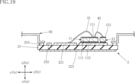
- Each wire 47 has one end connected to the buffer section 48 disposed on the first electrode 111 (second metal layer 111b), and the other end connected to the conductor layer 227.
- Each wire 47 connects the buffer section 48 and each conductor layer 227 to each other. Further, in this embodiment, since only a relatively small current flows through each wire 46, 47, the diameter of each wire 46, 47 is approximately the same as that of each wire 43, 44 (for example, about 150 ⁇ m). Note that the diameter of each wire 46, 47 is not limited.
- the constituent material of the wire 46 is the second metal.
- the second metal is Cu, which is the same as the second metal layer 111b of the first electrode 111.
- the constituent material of the wire 47 is a first metal whose thermoelectric power is different from that of the second metal. Thermoelectric power is the thermoelectromotive force per 1K when a temperature difference is created between both ends of a conductive substance.
- the first metal is constantan (an alloy of Cu and Ni: 55Cu-45Ni).
- the wire 46 (Cu), the second metal layer 111b (Cu) of the first electrode 111, the buffer portion 48 (which is Cu as described later), and the wire 47 (constantan) function as a thermocouple.
- thermocouples based on Cu and constantan are widely known as T-type thermocouples.
- a contact point 47a between the wire 47 and the buffer portion 48 corresponds to a temperature measuring contact point (thermal contact point) of a thermocouple.
- the contact between the wire 46 and the conductor layer 226 and the contact between the wire 47 and the conductor layer 227 correspond to a reference junction (cold junction) of the thermocouple.
- a voltage is generated between the reference junctions depending on the temperature difference between the reference junction and the temperature measurement junction.
- the temperature detection terminals 36 and 37 output the voltage between the reference junctions to the drive device 7 as a signal for detecting the temperature of the semiconductor element 11.
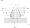
- the buffer section 48 is bonded to the first electrode 111 (second metal layer 111b), and is a member for absorbing impact on the semiconductor element 11 when the wire 47 is bonded.
- the wire 47 is made of a first metal (constantan). Therefore, the wire 47 has a larger Vickers hardness than the second metal layer 111b whose constituent material is Cu. Furthermore, since the second metal layer 111b is formed by plating, its thickness is relatively small (50 ⁇ m or less). Therefore, if the wire 47 is bonded to the first electrode 111 by wedge bonding, the semiconductor element 11 may be damaged by the impact.
- the buffer part 48 is electrically connected to the second metal layer 111b of the first electrode 111, and the wire 47 is electrically connected to the buffer part 48, thereby absorbing the impact on the semiconductor element 11. control damage.
- the constituent material of the buffer section 48 is Cu, which is the same as the second metal layer 111b of the first electrode 111 and the wire 46.
- the buffer section 48 is a piece of wire made by joining wire materials together by wedge bonding. As will be described later, unlike normal wire bonding, the buffer portion 48 is formed by first bonding, stretching the wire material a little, and immediately cutting it. In this embodiment, the buffer section 48 is formed using the same wire material as each wire 41, 42, 45. Therefore, the constituent material of the buffer section 48 is Cu, similarly to the wires 41, 42, and 45. Further, the dimension in the direction perpendicular to the extending direction of the buffer section 48 (hereinafter sometimes referred to as "diameter") is approximately the same as the diameter of each wire 41, 42, 45 (for example, approximately 400 ⁇ m), and each It is larger than the diameter of wire 47. Note that the buffer portion 48 may be formed using a wire material different from that of the wires 41, 42, and 45, and the diameter of the buffer portion 48 is not limited.
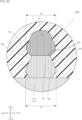
- the shape of the buffer portion 48 is such that a substantially cylindrical wire material is pressed against the first electrode 111 by wedge bonding and crushed.
- the buffer portion 48 includes a top surface 481, a bottom surface 482, a pair of pressed surfaces 483, and a cut surface 484.
- the top surface 481 and the bottom surface 482 face oppositely to each other in the z direction.
- the top surface 481 faces the z2 side in the z direction, and the bottom surface 482 faces the z1 side in the z direction.
- the bottom surface 482 is a flat surface in contact with the first electrode 111.
- a wire 47 is bonded to the top surface 481.
- the pair of pressed surfaces 483 are arranged on both sides of the top surface 481 when viewed in the z direction (in the example of FIG. 7, on both sides in the x direction). As will be described later, the pair of pressed surfaces 483 are surfaces formed by pressing the guide groove of the wedge, and the shape of the guide groove of the wedge appears. The pair of pressed surfaces 483 are each flat, and are further away from each other toward the z1 side in the z direction.
- the cut surface 484 is a surface cut by wedge bonding, and faces the direction in which the buffer portion 48 extends (in the example of FIG. 6, the y-direction y1 side). As shown in FIG. 6, the cut surface 484 is inclined with respect to a plane perpendicular to the direction in which the buffer portion 48 extends. Note that the shape of the buffer section 48 is not limited.
- the direction in which the buffer portion 48 extends (the y direction in the example of FIG. 6) is the same as the direction in which the wire 47 extends.
- the dimension D1 in the direction in which the pair of pressed surfaces 483 of the buffer section 48 are lined up (the x direction in the example of FIG. 7) is derived from the diameter of the wire material, and is therefore approximately the same as the diameter of the wire material.
- the dimension D2 of the wire 47 in the same direction is derived from the diameter of the wire material of the wire 47, and is therefore approximately the same as the diameter of the wire 47.
- Dimension D1 is larger than dimension D2 and larger than the diameter of wire 47.
- the dimension D1 is twice or more the dimension D2.
- the wire 47 is included in the top surface 481 in the direction in which the pair of pressed surfaces 483 are lined up (the x direction in the example of FIG. 7). Note that the wire 47 may protrude from the top surface 481.
- the resin member 5 is an electrically insulating semiconductor sealing material.
- the resin member 5 includes the entire plurality of semiconductor elements 11, the plurality of semiconductor elements 12, the insulating substrate 21, the main surface metal layer 22, the plurality of wires 41 to 47, and the plurality of buffer sections 48, and a part of each of the terminals 3. and covers.
- the constituent material of the resin member 5 is, for example, epoxy resin. Note that the constituent material of the resin member 5 is not limited.
- the resin member 5 is formed, for example, by transfer molding using a mold. Note that the method for forming the resin member 5 is not limited. As shown in FIGS. 2, 4, and 5, the resin member 5 has a resin main surface 51, a resin back surface 52, and a plurality of resin side surfaces 531 to 534.
- the resin main surface 51 and the resin back surface 52 face opposite to each other in the z direction.
- the main resin surface 51 faces the z2 side in the z direction
- the resin back surface 52 faces the z1 side in the z direction.
- the back metal layer 23 is exposed from the resin back surface 52, and the resin back surface 52 and the surface of the back metal layer 23 facing in the z direction z1 are flush with each other.
- Each of the plurality of resin side surfaces 531 to 534 is connected to both the resin main surface 51 and the resin rear surface 52, and is sandwiched between them. As shown in FIG. 2, the two resin side surfaces 531 and 532 face oppositely to each other in the x direction.
- the resin side surface 531 is a surface disposed on the x1 side in the x direction and facing the x1 side in the x direction.
- the resin side surface 532 is a surface disposed on the x2 side in the x direction and facing the x2 side in the x direction.
- the two resin side surfaces 533 and 534 face opposite to each other in the y direction.
- the resin side surface 533 is a surface disposed on the y1 side in the y direction and facing the y1 side in the y direction.
- the resin side surface 534 is a surface disposed on the y2 side in the y direction and facing the y2 side in the y direction.
- the resin side surfaces 531 to 534 each have a surface that is connected to the resin main surface 51 and slopes closer to each other toward the resin main surface 51. That is, the portion of the resin member 5 surrounded by the inclined surfaces connected to the main resin surface 51 has a tapered shape in which the cross-sectional area in the xy plane becomes smaller toward the main resin surface 51. Furthermore, the resin side surfaces 531 to 534 each have a surface that is connected to the resin back surface 52 and slopes closer to each other toward the resin back surface 52. That is, the portion of the resin member 5 surrounded by the inclined surfaces connected to the main resin surface 51 has a tapered shape in which the cross-sectional area in the xy plane becomes smaller toward the resin back surface 52. Note that the shape of the resin member 5 shown in FIGS. 1 to 5 is an example. The shape of the resin member 5 is not limited to the illustrated shape.
- the driving device 7 is a device that drives the semiconductor device A10, and as shown in FIG. 8, is attached to the z-direction z2 side of the semiconductor device A10.
- the drive device 7 includes a substrate 71, terminals 723, 724, 725, and a plurality of terminals 721, 722, respectively.
- the substrate 71 is, for example, flat and has electrical insulation properties.
- the constituent material of the substrate 71 is not limited.
- Substrate 71 has a main surface 711 and a back surface 712.
- the main surface 211 and the back surface 712 face opposite to each other in the z direction.
- the main surface 711 faces the z2 side in the z direction.
- the back surface 712 faces the z1 side in the z direction.
- Wiring is formed on the main surface 711, and external connectors and a large number of electronic components are mounted, but in FIG. 8, the wiring, external connectors, electronic components, etc. on the main surface 711 are omitted. There is.
- Each of the terminals 721 to 725 is a cylindrical metal member, and is inserted into a through hole that penetrates in the z direction from the main surface 711 to the back surface 712 of the substrate 71.
- Each of the terminals 721 to 725 is electrically connected to a wiring formed on the main surface 711, respectively.
- the terminal portions 332, 342, 352, 362, and 372 of the terminals 33 to 37 of the semiconductor device A10 are inserted into each of the terminals 721 to 725, respectively, and are joined by, for example, solder.
- the signal terminal 33 is connected to the terminal 723.
- the detection terminal 34 is connected to the terminal 724.
- the detection terminal 35 is connected to the terminal 725.
- Five terminals 721 are arranged like the temperature detection terminals 36, and each terminal 721 is connected to the temperature detection terminal 36, respectively. Since the temperature detection terminal 36 is electrically connected to the wire 46 via the conductor layer 226, the terminal 721 is electrically connected to the wire 46.
- Five terminals 722 are arranged like the temperature detection terminals 37, and each terminal 722 is connected to the temperature detection terminal 37, respectively. Since the temperature detection terminal 37 is electrically connected to the wire 47 via the conductor layer 227, the terminal 722 is electrically connected to the wire 47.
- the drive device 7 includes a plurality of relative temperature detection sections 73, a plurality of reference junction compensation sections 74, an overheat protection section 75, and a drive control section 76 as functional configurations.
- the drive control unit 76 is a functional configuration that controls the switching operation of each semiconductor element 11, and is realized by, for example, a gate drive IC.
- the drive control section 76 includes a drive circuit DR, a Miller clamp circuit MC, and the like.
- the drive control unit 76 generates a drive signal based on a control signal input from the outside, and outputs the drive signal to the semiconductor device A10 via the terminal 723.
- the semiconductor device A10 receives a drive signal from the signal terminal 33 connected to the terminal 723, and controls the switching operation of each semiconductor element 11. Further, the drive control unit 76 receives a signal from the detection terminal 34 of the semiconductor device A10 via the terminal 724, and receives a signal from the detection terminal 35 via the terminal 725. Note that the specific circuit configuration and aspect of the drive control section 76 are not limited.
- the relative temperature detection section 73 and the reference junction compensation section 74 are functional configurations for detecting the temperature of the semiconductor element 11.
- Five relative temperature detectors 73 and five reference junction compensators 74 are provided, each corresponding to the number of semiconductor elements 11 of semiconductor device A10.
- Each relative temperature detection section 73 receives voltage from a pair of temperature detection terminals 36 and 37 of the semiconductor device A10 via a pair of terminals 721 and 722.
- the voltage is the voltage between the reference junction of the thermocouple that includes the wire 46, the second metal layer 111b of the first electrode 111, the buffer section 48, and the wire 47, and is caused by the temperature difference between the reference junction and the temperature measurement junction.
- the voltage is appropriate. That is, the voltage corresponds to the relative temperature of the semiconductor element 11 with respect to the temperature of the reference junction.
- Each relative temperature detection section 73 detects the relative temperature of the corresponding semiconductor element 11 based on the input voltage.
- Each reference junction compensation section 74 converts the relative temperature detected by the corresponding relative temperature detection section 73 into an absolute temperature.
- Each reference junction compensation section 74 includes a temperature detection section having, for example, a diode, disposed adjacent to the corresponding terminal 721, 722. Note that the temperature detection section may include a temperature sensor such as a thermistor.
- the temperature detection terminals 36 and 37 connected to the terminals 721 and 722 are connected to the conductor layers 226 and 227.
- the temperature detection section indirectly detects the temperature of the reference junction of the thermocouple by detecting the temperature of the terminals 721 and 722.
- the reference junction compensation unit 74 converts the relative temperature detected by the corresponding relative temperature detection unit 73 into an absolute temperature by adding the temperature of the reference junction detected by the temperature detection unit.
- the reference junction compensation section 74 outputs the absolute temperature of the corresponding semiconductor element 11 to the overheat protection section 75 .
- the specific circuit configurations of the relative temperature detection section 73 and the reference junction compensation section 74 are not limited.
- the following configuration may be used. That is, the relative temperature detection section 73 transmits the voltage between the pair of terminals 721 and 722 to the reference junction compensation section 74 as a voltage according to the relative temperature of the corresponding semiconductor element 11.
- the reference junction compensation unit 74 converts the voltage corresponding to the temperature of the reference junction detected by the temperature detection unit into a voltage corresponding to the thermoelectromotive force of the thermocouple, and adds it to the voltage transmitted from the relative temperature detection unit 73. and outputs it to the overheat protection section 75.
- a voltage corresponding to the absolute temperature of the semiconductor element 11 is input to the overheat protection section 75 .
- the overheat protection unit 75 detects an overheat abnormality in the corresponding semiconductor element 11 based on the absolute temperature input from each reference junction compensation unit 74.
- the overheat protection section 75 outputs an abnormality detection signal to the drive control section 76 when the absolute temperature input from each reference junction compensation section 74 becomes equal to or higher than the threshold temperature.
- the drive control unit 76 receives the abnormality detection signal, it stops driving the semiconductor device A10 by stopping the output of the drive signal.
- the specific circuit configuration of the overheat protection section 75 is not limited.
- the overheat protection section 75 may include a comparator that generates an abnormality detection signal when the voltage according to the absolute temperature input from the reference junction compensation section 74 becomes equal to or higher than the voltage according to the threshold temperature. .
- FIG. 10 is a flowchart illustrating an example of a method for manufacturing the semiconductor device A10.
- 11 to 14 and 17 to 21 are diagrams showing steps in an example of the method for manufacturing the semiconductor device A10.
- 11 to 14 and FIGS. 19 to 20 are cross-sectional views corresponding to FIG. 4.
- FIG. 17 is a partially enlarged plan view corresponding to FIG. 3.
- FIG. 18 is a cross-sectional view and corresponds to FIG. 7.
- FIG. 21 is a front view. 15 and 16 are diagrams for explaining wedge bonding. Note that the x direction, y direction, and z direction shown in FIGS. 11 to 21 indicate the same directions as in FIGS. 1 to 8.
- the manufacturing method of the semiconductor device A10 includes a support member forming step (S1), a lead frame bonding step (S2), a semiconductor element mounting step (S3), a wire forming step (S4), and a resin forming step ( S5), and a frame cutting step (S6).
- the support member forming step (S1) is a step of forming the support member 2.
- the insulating substrate 91 is prepared (S11).
- the insulating substrate 91 is made of ceramic, for example, and has a main surface 911 and a back surface 912 facing oppositely to each other in the z direction.
- a main surface metal layer 22 is formed on the main surface 911 of the insulating substrate 91 (S12).
- the main surface metal layer 22 is formed by forming a base layer covering the entire main surface 911 by, for example, electroless plating or sputtering, forming a mask, forming a plating layer by electrolytic plating, and etching to eliminate the need for the base layer.
- a back metal layer 23 is formed on the back surface 912 of the insulating substrate 91 (S13).
- the back metal layer 23 is formed, for example, by electroless plating. Note that by using a DBC (Direct Bonding Copper) substrate in which Cu foil is bonded to the main surface 911 and the back surface 912 of the insulating substrate 91, the main surface metal is bonded to the insulating substrate 91 by patterning the Cu foil on the main surface 911 side. Layer 22 and back metal layer 23 may be formed.
- the insulating substrate 91 is cut (S14).
- the insulating substrate 21 is formed by cutting the insulating substrate 91. Through the above steps, the support member 2 is formed.
- the lead frame 92 that will become each terminal 3 is prepared.
- the lead frame 92 includes a portion that becomes each terminal 3, and further has a frame to which a plurality of terminals 3 are connected. Note that the shape etc. of the lead frame 92 are not limited at all.
- a conductive bonding paste is placed at the position of the main surface metal layer 22 where each terminal 3 is to be bonded, and as shown in FIG. do. For example, a portion of the lead frame 92 that will become the detection terminal 35 is bonded to the conductive layer 224. Further, a portion of the lead frame 92 that will become the detection terminal 36 is joined to the conductive layer 226. Note that the method of joining the lead frame 92 is not limited.
- a conductive bonding paste 93 is placed in the region of the conductor layer 223 where the semiconductor elements 11 and 12 are to be placed.
- the conductive bonding paste 93 is, for example, solder, silver paste, or sintered metal.
- the plurality of semiconductor elements 11 and the plurality of semiconductor elements 12 are attached to the conductive bonding paste 93, heated, and then cooled.
- the conductive bonding paste 93 interposed between the conductive layer 223 and the semiconductor element 11 becomes the conductive bonding material 110, and the semiconductor element 11 is bonded to the conductive layer 223 via the conductive bonding material 110.
- Ru Further, the conductive bonding paste 93 interposed between the conductive layer 223 and the semiconductor element 12 becomes the conductive bonding material 120, and the semiconductor element 12 is bonded to the conductive layer 223 via the conductive bonding material 120.
- the wires 41 to 47 and the buffer portion 48 are formed by wedge bonding. Wedge bonding is performed using a wedge tool.
- 15 and 16 show an example of a wedge tool.
- FIG. 15 is a front view showing the entire wedge tool 6.
- FIG. 16 is a cross-sectional view of the wedge tool 6 shown in FIG. 15 taken along the line XVI-XVI.
- the wedge tool 6 includes a wedge 61, a wire guide 62, and a cutter 63.
- the wedge 61 presses the wire material 69 against the object to be welded 68 and joins it by ultrasonic vibration.
- the wedge 61 has a guide groove 611 formed therein.
- the guide groove 611 is provided at the lower end of the wedge 61 (on the z1 side in the z direction).
- the guide groove 611 has a V-shaped cross section and a pair of inner surfaces 611a, as shown in FIG. 16.
- Ultrasonic vibration is applied to the wedge 61 in the direction of the white arrow shown in FIG. 15 when the wire material 69 is joined.
- the wire guide 62 is fixed to the wedge 61 and guides a wire material 69 wound on a wire reel (not shown) to the wedge 61.
- Cutter 63 cuts wire material 69.
- the cutter 63 is located adjacent to the wedge 61.
- the wire guide 62 and the cutter 63 are placed on opposite sides of the wedge 61.
- the wedge 61 is pressed against the welding object 68 with the wire material 69 disposed in the guide groove 611 and is subjected to vibration. Thereby, the tip portion of the wire material 69 and the bonding target 68 are bonded by ultrasonic welding (first bonding). In the case of normal wire bonding, the wedge tool 6 then moves while pulling out the wire material 69, joins the wire material 69 to another bonding target 68 by ultrasonic welding (second bonding), and transfers the wire material 69 to the cutter 63. Cut by. As a result, bonding wires having both ends bonded to the two objects 68 to be bonded are formed. On the other hand, when forming the buffer portion 48, the wedge tool 6 moves a little in the direction of the black arrow shown in FIG. 15, and then cuts the wire material 69 with the cutter 63. As a result, the wire piece, which is the cut end of the wire material 69, is joined as the buffer portion 48.
- a buffer portion 48 is formed on the first electrode 111 of the semiconductor element 11 (S41).
- Each buffer portion 48 is formed near the center of each first electrode 111 in the y direction so as to extend in the y direction toward the x1 side in the x direction. Since the wire 47 is bonded as described later, the buffer portion 48 is arranged in accordance with the position where the wire 47 is bonded, and is formed to extend in the same direction as the wire 47 extends.
- the buffer section 48 is formed by joining the tip of a wire material 691 (for example, a Cu wire) to the first electrode 111 by ultrasonic welding, moving the wedge tool 6 a little, and then cutting the wire material 691 with the cutter 63.
- Each pressed surface 483 is a surface whose cross section is retracted toward the central axis Ox side of the wire material 691 from the outer circumferential surface 489 having an arcuate shape. Since each inner surface 611a is flat, each pressed surface 483 is flat. Furthermore, as the wire material 691 is cut by the cutter 63, a cut surface 484 is formed in the buffer portion 48, as shown in FIG. The cutting surface 484 is inclined with respect to a plane perpendicular to the direction in which the buffer section 48 extends, depending on the shape of the cutter 63.
- wires 41, 42, and 45 are formed by wedge bonding (S42).
- the same wedge tool 6 and the same wire material 691 as in the formation of the buffer section 48 are used, but unlike the formation of the buffer section 48, normal wire bonding is performed.
- the wire 41 is formed to connect the first electrode 111 of the semiconductor element 11 and the conductor layer 221.
- the wire 42 is formed to connect the conductor layer 221 and the conductor layer 225.
- the wire 45 is formed to connect the first electrode 111 and the anode electrode 121 of the semiconductor element 12 .
- the order of forming the wires 41, 42, and 45 is not limited. Further, the order of the step S41 and the step S42 may be reversed.
- wires 43, 44, and 46 are formed by wedge bonding (S43).
- a wire material 692 having the same constituent material as the wire material 691 used in S42 but having a different diameter is used.
- the diameter of wire material 692 is smaller than the diameter of wire material 691.
- the wire 43 is formed to connect the second electrode 112 of the semiconductor element 11 and the conductor layer 222.
- the wire 44 is formed to connect the first electrode 111 and the conductor layer 224.
- the wire 46 is formed to connect the first electrode 111 and the conductor layer 226. Note that the order of forming the wires 43, 44, and 46 is not limited.
- the wire 47 is formed by wedge bonding (S44).
- a wire material 693 whose constituent material is different from the wire material 692 used in S43 is used.
- the wire materials 691 and 692 whose constituent material is Cu are used in S41 to S43, but the wire material 693 whose constituent material is constantan is used in S44.
- the diameter of the wire material 693 used in S44 is approximately the same as the diameter of the wire material 692 used in S43, and smaller than the diameter of the wire material 691 used in S42.
- Wire 47 is formed using the same equipment and in the same manner as wires 43, 44, and 46, except that the wire material 693 used is different.
- the wire 47 is first joined to the top surface 481 of the buffer section 48 that is joined to the first electrode 111.
- FIG. 21 shows a state in which the wedge tool 6 is moving while pulling out the wire material 693 (wire 47) after bonding to the buffer portion 48 (first bonding).
- the wire 47 is bonded onto the top surface 481 along the direction in which the buffer section 48 extends, and is formed to extend in that direction.
- the wire 47 is made of constantan and is harder than the wire 46 made of Cu, but it is not directly joined to the first electrode 111 but is joined to the buffer section 48 . Therefore, the impact on the semiconductor element 11 during bonding is suppressed.
- the wedge tool 6 moves to bond the wire material 693 to the conductor layer 227 by ultrasonic welding (second bonding), and cut the wire material 693 with the cutter 63.
- the wire 47 is formed so as to connect the buffer section 48 joined to the first electrode 111 and the conductor layer 227 (see FIGS. 3 and 6).
- the step S44 may be performed before the step S43.
- the wire 46 is joined to the first electrode 111, and the wire 47 is joined to the buffer section 48 joined to the first electrode 111, thereby forming a thermocouple.
- a part of the lead frame 92, a part of the support member 2, the plurality of semiconductor elements 11 and 12, the plurality of wires 41 to 47, and the buffer section 48 are surrounded by a mold.
- a liquid resin material is injected into the space defined by the mold.
- the resin member 5 is obtained by curing this resin material.
- the lead frame 92 is cut at an appropriate location exposed from the resin member 5. Thereby, each terminal 3 is divided from each other. After this, the above-described semiconductor device A10 is obtained by performing a process such as bending each terminal 3 as necessary.
- the buffer section 48 is joined to the first electrode 111.
- the wire 47 is not directly connected to the first electrode 111 but is connected to the buffer section 48 . Since the buffer portion 48 absorbs the impact when the wires 47 are bonded, the semiconductor device A10 can alleviate the impact applied to the semiconductor element 11. Further, the buffer portion 48 is formed using a wire material 691 by wedge bonding.
- the buffer section 48 can be formed using the same wedge tool 6 and the same wire material 691 as those for forming the wires 41, 42, and 45 (S42), so the manufacturing process can be simplified by forming it continuously with the step S42. can be converted into Therefore, the semiconductor device A10 can suppress an increase in manufacturing cost.
- the dimension D1 in the direction in which the pair of pressed surfaces 483 of the buffer section 48 are lined up is the dimension D1 in the direction in which the pair of pressed surfaces 483 of the buffer section 48 are arranged. It is larger than dimension D2 (comparable to the diameter of wire material 693 for forming wire 47). Therefore, when joining the wire 47 to the buffer portion 48, it is possible to prevent the wire 47 from slipping off the top surface 481. Further, according to the present embodiment, the wire 47 is enclosed in the top surface 481 in the direction in which the pair of pressed surfaces 483 are lined up. Therefore, when joining the wire 47 to the buffer portion 48, it is possible to further suppress the wire 47 from slipping off the top surface 481.
- the direction in which the buffer portion 48 extends matches the direction in which the wire 47 extends. Therefore, it is easier to join the wire 47 to the buffer section 48 compared to the case where the directions do not match.
- one end of the wire 46 is bonded to the second metal layer 111b of the first electrode 111, and one end of the wire 47 is bonded to the buffer portion 48 bonded to the second metal layer 111b. are joined.
- the constituent material of the wire 46 is a second metal (Cu), which is the same metal (Cu) as the constituent material of the second metal layer 111b and the buffer section 48.
- the constituent material of the wire 47 is a first metal (constantan) having a different thermoelectric power from the second metal.
- the wire 46, the second metal layer 111b, the buffer section 48, and the wire 47 function as a thermocouple, and the temperature can be detected by using the contact 47a between the wire 47 and the buffer section 48 as a temperature measuring junction of the thermocouple.
- the contact 47a is in contact with a buffer section 48 through which heat from the semiconductor element 11 is appropriately transmitted.
- the semiconductor device A10 can detect the temperature of each semiconductor element 11 with higher accuracy than when the temperature sensor is placed near the semiconductor element 11.
- the thermocouple functions as a T-type thermocouple.
- the wires 46 and 47 are formed by the bonding wire forming method similarly to the wires 41 to 45. Therefore, wires 46 and 47 can be formed using the same equipment and using the same techniques as wires 41-45. In particular, wire 46 can be formed using the same wire material 692 as wires 43, 44 and in the same process as wires 43, 44. Therefore, the manufacturing process is not complicated due to the formation of the structure for detecting temperature.
- the drive device 7 includes a relative temperature detection section 73 and a reference junction compensation section 74. Therefore, the drive device 7 converts the relative temperature of each semiconductor element 11 detected by the thermocouple formed in the semiconductor device A10 into an absolute temperature, which can be used for overheat protection.
- the present invention is not limited to this.
- the first metal and the second metal may be metals having different electrolytic abilities.
- the second metal may be Cu and the first metal may be Al.
- Cu and Al have the same polarity but different electrolytic capacities, so the wire 46, the second metal layer 111b, the buffer section 48 (Cu), and the wire 47 (Al) can be used as a thermocouple. Function.
- Al is commonly used as a bonding wire, and compared to constantan wire, it is easily available at a low price.
- the combination of the first metal and the second metal may be Chromel (registered trademark) (90Ni-10Cr) and Alumel (registered trademark) (94Ni-3Al-1Si-2Mg) like a K-type thermocouple. , Fe and constantan as in a J-type thermocouple, or chromel and constantan as in an E-type thermocouple.
- the combination of the first metal and the second metal is not limited to those described above.
- the present invention is not limited to this. Any one of the plurality of terminals 3 may be spaced apart from the main surface metal layer 22 and joined to the insulating substrate 21. In this case, the terminal 3 is electrically connected to the main surface metal layer 22 using a bonding wire or the like.
- FIG. 22 is a diagram for explaining a semiconductor device A11 according to a first modification of the first embodiment.
- FIG. 22 is a partially enlarged cross-sectional view of the semiconductor device A11, and corresponds to FIG. 7.
- the semiconductor device A11 differs from the semiconductor device A10 in that the dimension D1 of the buffer portion 48 and the dimension D2 of the wire 47 are approximately the same.
- the wire material 691 and the wire material 693 have the same (or substantially the same) diameter. Therefore, the dimension D1 of the buffer portion 48 formed using the wire material 691 and the dimension D2 of the wire 47 formed using the wire material 693 are approximately the same.
- the wire material 692 also has the same diameter as the wire material 691, and the diameters of the wires 41 to 47 are all approximately the same. According to this modification, the diameters of the wire materials 691 to 693 are the same (or substantially the same), and the wires 41 to 47 and the buffer section 48 can be formed using the same wedge tool 6, so that the semiconductor device A11 can be manufactured in the manufacturing process. can be further simplified.
- the wire 47 can be joined onto the top surface 481 of the buffer section 48.
- the dimension D1 is larger than the dimension D2
- the diameter of the wire material 691 is larger than the diameter of the wire material 693.
- FIG. 23 is a diagram for explaining a semiconductor device A12 according to a second modification of the first embodiment.
- FIG. 23 is a partially enlarged plan view of the semiconductor device A12, and corresponds to FIG. 3.
- the resin member 5 is shown.
- the semiconductor device A12 differs from the semiconductor device A10 in that the wires 41, 43 to 46 are also bonded to the buffer section.
- the wire 47 not only the wire 47 but also the wires 44 and 46 are joined to the buffer section 48 that is joined to the first electrode 111.
- the wire 43 is connected to a buffer section 48 that is connected to the second electrode 112.
- the wires 41 and 45 are joined to a buffer section 48' that is joined to the first electrode 111.
- Buffer 48' is formed similarly to buffer 48 using a wire material having a larger diameter than wire material 691 used to form buffer 48.
- the wires 41 to 46 are made of Cu, and although not as hard as the wire 47 (constantan), they are sufficiently hard compared to Al used in conventional wires. Therefore, if the wires 41 to 46 are directly bonded to the first electrode 111, the semiconductor element 11 may be damaged by the impact of bonding. According to this modification, the semiconductor device A12 can reduce the impact applied to the semiconductor element 11 when the wires 41 to 46 are bonded, and can suppress damage to the semiconductor element 11.
- FIG. 24 is a diagram for explaining a semiconductor device A13 according to a third modification of the first embodiment.
- FIG. 24 is a partially enlarged plan view of the semiconductor device A13, and corresponds to FIG. 3.
- the resin member 5 is shown.
- the semiconductor device A13 differs from the semiconductor device A10 in that the wire 47 is bonded to the wire 41.
- the semiconductor device A13 does not include the buffer section 48.
- Each wire 47 is bonded to a bonding portion 41a, which is a portion of the wire 41 bonded to the first electrode 111, instead of the buffer portion 48.
- the bonding portion 41a of the wire 41 absorbs the impact when the wire 47 is bonded, so that the semiconductor device A13 can alleviate the impact applied to the semiconductor element 11. Further, since the originally necessary wire 41 is used and the buffer section 48 is not provided separately, the manufacturing process of the semiconductor device A13 can be further simplified.
- FIG. 25 is a diagram for explaining a semiconductor device A14 according to a fourth modification of the first embodiment.
- FIG. 25 is a partially enlarged plan view of the semiconductor device A14, and corresponds to FIG. 3.
- the resin member 5 is shown.
- the semiconductor device A14 differs from the semiconductor device A10 in that the wire 47 is joined to the wire 49.
- the first electrode 111 of the semiconductor element 11 is connected to the first electrode 111 of the adjacent semiconductor element 11. and are electrically connected by a wire 49.
- the constituent material of the wire 49 is not limited, but in this modification, it is Cu, like the wires 41 to 46.
- the wire 49 extends in the x direction, which is the direction in which the semiconductor elements 11 are arranged.
- the semiconductor device A14 does not include the buffer section 48. Each wire 47 is bonded to a bonding portion 49a, which is a portion of the wire 49 bonded to the first electrode 111, instead of the buffer portion 48.
- the bonding portion 49a of the wire 49 absorbs the impact when the wire 47 is bonded, the semiconductor device A14 can reduce the impact applied to the semiconductor element 11. Further, since the originally necessary wire 49 is used and the buffer section 48 is not provided separately, the manufacturing process of the semiconductor device A14 can be further simplified. Note that in this modification, the direction in which the joint portion 49a extends does not match the direction in which the wire 47 extends, but it is possible to join the wire 47 to the joint portion 49a.
- each wire 47 can be joined to the joint part of any wire joined to the first electrode 111 instead of the buffer part 48. Furthermore, although it is desirable that the extending direction of the bonded portion coincides with the extending direction of the wire 47, it is possible to bond the wire 47 even if the direction does not match.
- 26 to 28 show other embodiments of the present disclosure.
- the same or similar elements as in the above embodiment are given the same reference numerals as in the above embodiment, and redundant explanation will be omitted.
- FIG. 26 and 27 are diagrams for explaining a semiconductor device A20 according to a second embodiment of the present disclosure.
- FIG. 26 is a partially enlarged plan view showing the semiconductor device A20, and corresponds to FIG. 3.
- the resin member 5 is shown in FIG. 26.
- FIG. 27 is a cross-sectional view taken along line XXVII-XXVII in FIG. 26.
- the semiconductor device A20 according to the present embodiment differs from the semiconductor device A10 according to the first embodiment in that the constituent material of the wires 41 to 45 is Al.
- the configuration and operation of other parts of this embodiment are similar to those of the first embodiment. Note that each part of the first embodiment and each modification example described above may be combined arbitrarily.
- the constituent material of the wires 41 to 45 according to this embodiment is Al.
- the first electrode 111 of the semiconductor element 11 according to the present embodiment does not include the second metal layer 111b, and the first metal layer 111a whose constituent material is Al, as shown in FIG. located on the surface.
- the wire 44 is joined to the buffer section 48 that is joined to the first electrode 111, and the wires 41 and 45 are joined to the buffer section 48' that is joined to the first electrode 111.
- Buffer section 48' is formed in the same manner as buffer section 48 using wire material having a larger diameter than wires 41,45.
- the material of the buffer portions 48, 48' is Al.
- the semiconductor device A20 can alleviate the shock applied to the semiconductor element 11. Further, since the buffer portions 48, 48' are formed by wedge bonding, the manufacturing process can be simplified. Therefore, the semiconductor device A20 can suppress an increase in manufacturing cost. Furthermore, the semiconductor device A20 has the same configuration as the semiconductor device A10, and thus has the same effects as the semiconductor device A10. As can be understood from this embodiment, the semiconductor element 11 is not limited to the case where the first electrode 111 includes the second metal layer 111b.
- FIG. 28 is a diagram for explaining a semiconductor device A30 according to a third embodiment of the present disclosure.
- FIG. 28 is a partially enlarged sectional view showing the semiconductor device A30.
- the semiconductor device A30 according to the first embodiment further includes a terminal 39 extending close to the semiconductor element 11, and the wire 41 is formed so as to straddle the terminal 39. different from.
- the configuration and operation of other parts of this embodiment are similar to those of the first embodiment. Note that each part of the first to second embodiments and each modification example described above may be combined arbitrarily.
- the semiconductor device A30 further includes a terminal 39 extending close to the semiconductor element 11.
- the wire 41 is formed to straddle the terminal 39 in the z direction z2 side. Further, the wire 41 is bonded to a buffer portion 48' that is bonded to the second metal layer 111b of the first electrode 111. Buffer 48' is formed similarly to buffer 48 using wire material having a larger diameter than wire 41. On the other hand, the wire 45 is directly bonded to the second metal layer 111b of the first electrode 111.
- the semiconductor device A30 can alleviate the shock applied to the semiconductor element 11. Further, since the buffer portion 48' is formed by wedge bonding, the manufacturing process can be simplified. Therefore, the semiconductor device A30 can suppress an increase in manufacturing cost. Further, the semiconductor device A30 has the same configuration as the semiconductor device A10, and thus has the same effects as the semiconductor device A10.
- the wire 41 is formed so as to straddle the terminal 39 in the z direction z2 side. At this time, the wedge tool is largely pulled up in the z direction z2 side, thereby pulling the initially joined portion of the wire 41 in the z direction z2 side.
- the second metal layer 111b may peel off from the first metal layer 111a.
- the tension is relaxed by the buffer portion 48', and peeling of the second metal layer 111b can be suppressed.
- the buffer portions 48, 48' not only absorb shock during wire bonding, but also have the function of relieving tension applied after wire bonding.
- FIG. 29 is a diagram for explaining a semiconductor device A40 according to a fourth embodiment of the present disclosure.
- FIG. 29 is a plan view of the semiconductor device A40, and corresponds to FIG. 2.
- the outer shape of the resin member 5 is shown by an imaginary line (two-dot chain line) that is transparent through the resin member 5.
- the semiconductor device A40 according to this embodiment is different from the semiconductor device A10 according to the first embodiment in the package format. The configuration and operation of other parts of this embodiment are similar to those of the first embodiment. Note that each part of the first to third embodiments and each modification example described above may be combined arbitrarily.
- the package format of the semiconductor device A40 is DFN (Dual Flatpack No-leaded).
- the semiconductor device A40 includes leads 201 to 205, a semiconductor element 11, wires 41, 43, 46, 47, a buffer section 48, and a resin member 5.
- the semiconductor element 11, wires 41, 43, 46, 47, buffer section 48, and resin member 5 are the same as those in the first embodiment.
- the leads 201 to 205 are electrically connected to the semiconductor element 11.
- the leads 201 to 205 are made of metal, preferably Cu or Ni, or an alloy thereof, a 42 alloy, or the like. Note that the constituent material of the leads 201 to 205 is not limited, but is Cu in this embodiment.
- the leads 201 to 205 are, for example, lead frames formed by stamping a metal plate.
- the back surface 11b (not shown) of the semiconductor element 11 is bonded to the lead 201 via a conductive bonding material 110 (not shown).
- the third electrode 113 (drain electrode) (not shown) is electrically connected to the lead 201 via the conductive bonding material 110.
- the wire 41 has one end connected to the first electrode 111 (source electrode) and the other end connected to the lead 204.
- the wire 41 connects the first electrode 111 and the lead 204 to each other.
- the wire 43 has one end connected to the second electrode 112 (gate electrode) and the other end connected to the lead 205.
- the wire 43 connects the second electrode 112 and the lead 205 to each other.
- the wire 46 has one end connected to the first electrode 111 and the other end connected to the lead 202.
- the wire 47 has one end joined to the buffer section 48 joined to the first electrode 111 and the other end joined to the lead 203.
- Leads 202 and 203 serve as terminals for detecting the temperature of semiconductor element 11.
- the wire 47 is not directly joined to the first electrode 111 but is joined to the buffer section 48. Since the buffer portion 48 absorbs the impact when the wires 47 are bonded, the semiconductor device A40 can alleviate the impact applied to the semiconductor element 11. Further, the buffer portion 48 is formed using a wire material 691 by wedge bonding. Since the buffer portion 48 can be formed using the same wedge tool 6 and the same wire material 691 as those used to form the wire 41 (S42), the manufacturing process can be simplified by forming it continuously with the step S42. Therefore, the semiconductor device A40 can suppress an increase in manufacturing cost.
- a semiconductor device and a method for manufacturing a semiconductor device according to the present disclosure are not limited to the embodiments described above.
- the specific configuration of each part of the semiconductor device according to the present disclosure and the specific processing of each step of the semiconductor device manufacturing method according to the present disclosure can be variously changed in design.
- the present disclosure includes the embodiments described in the appendix below.
- a semiconductor element (11) having an element main surface (11a) and an element back surface (11b) facing opposite to each other in the thickness direction (z direction), and a first electrode (111) disposed on the element main surface. and, a buffer part (48) electrically connected to the first electrode; a first wire (47) electrically connected to the buffer portion and containing a first metal;
- the buffer section is a bottom surface (482) in contact with the first electrode; a top surface (481) facing opposite to the bottom surface in the thickness direction; a pair of pressed surfaces (483) that are flat and arranged on both sides of the top surface when viewed in the thickness direction; Equipped with The pair of pressed surfaces are further apart from each other in the thickness direction toward the bottom surface.
- Appendix 3. the first wire is joined to the top surface;
- the dimension (D1) of the buffer portion in the direction in which the pair of pressed surfaces are lined up is larger than the diameter (D2) of the first wire;
- the buffer section is a second wire (41, 49) electrically connected to the first electrode.
- the buffer section contains Cu.
- the first electrode includes a metal layer (111b) in contact with the buffer section,
- the metal layer is a plating layer containing Cu,
- Appendix 9. The dimension of the metal layer in the thickness direction is 50 ⁇ m or less, The semiconductor device according to appendix 7 or 8.
- the constituent material of the metal layer is the same as that of the buffer section,
- Appendix 11. the first wire has a greater Vickers hardness than the metal layer;
- Appendix 12. further comprising a third wire (46) containing a second metal having a different thermoelectric power from the first metal, the third wire is joined to the first electrode,
- Appendix 13 the first metal is constantan, the second metal is Cu;
- the direction in which the buffer section extends is the same as the direction in which the first wire extends.
Landscapes
- Wire Bonding (AREA)
Priority Applications (1)
| Application Number | Priority Date | Filing Date | Title |
|---|---|---|---|
| JP2024538890A JPWO2024029286A1 (https=) | 2022-08-03 | 2023-07-11 |
Applications Claiming Priority (2)
| Application Number | Priority Date | Filing Date | Title |
|---|---|---|---|
| JP2022-123758 | 2022-08-03 | ||
| JP2022123758 | 2022-08-03 |
Publications (1)
| Publication Number | Publication Date |
|---|---|
| WO2024029286A1 true WO2024029286A1 (ja) | 2024-02-08 |
Family
ID=89849207
Family Applications (1)
| Application Number | Title | Priority Date | Filing Date |
|---|---|---|---|
| PCT/JP2023/025566 Ceased WO2024029286A1 (ja) | 2022-08-03 | 2023-07-11 | 半導体装置、および、半導体装置の製造方法 |
Country Status (2)
| Country | Link |
|---|---|
| JP (1) | JPWO2024029286A1 (https=) |
| WO (1) | WO2024029286A1 (https=) |
Citations (12)
| Publication number | Priority date | Publication date | Assignee | Title |
|---|---|---|---|---|
| JP2000012605A (ja) * | 1998-06-18 | 2000-01-14 | World Metal:Kk | 半導体チップの電極部の形成方法 |
| JP2007149714A (ja) * | 2005-11-24 | 2007-06-14 | Matsushita Electric Ind Co Ltd | 基板およびその形成方法および半導体装置 |
| JP2009293986A (ja) * | 2008-06-03 | 2009-12-17 | Denso Corp | 半導体装置 |
| JP2010258286A (ja) * | 2009-04-27 | 2010-11-11 | Sanyo Electric Co Ltd | 半導体装置及びその製造方法 |
| JP2010278420A (ja) * | 2009-04-30 | 2010-12-09 | Nichia Corp | 半導体装置及びその製造方法 |
| JP2014203957A (ja) * | 2013-04-04 | 2014-10-27 | ローム株式会社 | 半導体装置および半導体装置の製造方法 |
| WO2014175343A1 (ja) * | 2013-04-25 | 2014-10-30 | 富士電機株式会社 | 半導体装置および半導体装置の製造方法 |
| JP2015037151A (ja) * | 2013-08-15 | 2015-02-23 | サンケン電気株式会社 | 半導体装置 |
| JP2015142059A (ja) * | 2014-01-30 | 2015-08-03 | 株式会社日立製作所 | パワー半導体モジュール |
| JP2019004137A (ja) * | 2017-05-29 | 2019-01-10 | ローム株式会社 | 半導体装置およびその製造方法 |
| JP2019159189A (ja) * | 2018-03-15 | 2019-09-19 | 住友大阪セメント株式会社 | 光変調器、及び光伝送装置 |
| JP2020113721A (ja) * | 2019-01-16 | 2020-07-27 | 富士電機株式会社 | 半導体装置および半導体装置の製造方法 |
-
2023
- 2023-07-11 WO PCT/JP2023/025566 patent/WO2024029286A1/ja not_active Ceased
- 2023-07-11 JP JP2024538890A patent/JPWO2024029286A1/ja active Pending
Patent Citations (12)
| Publication number | Priority date | Publication date | Assignee | Title |
|---|---|---|---|---|
| JP2000012605A (ja) * | 1998-06-18 | 2000-01-14 | World Metal:Kk | 半導体チップの電極部の形成方法 |
| JP2007149714A (ja) * | 2005-11-24 | 2007-06-14 | Matsushita Electric Ind Co Ltd | 基板およびその形成方法および半導体装置 |
| JP2009293986A (ja) * | 2008-06-03 | 2009-12-17 | Denso Corp | 半導体装置 |
| JP2010258286A (ja) * | 2009-04-27 | 2010-11-11 | Sanyo Electric Co Ltd | 半導体装置及びその製造方法 |
| JP2010278420A (ja) * | 2009-04-30 | 2010-12-09 | Nichia Corp | 半導体装置及びその製造方法 |
| JP2014203957A (ja) * | 2013-04-04 | 2014-10-27 | ローム株式会社 | 半導体装置および半導体装置の製造方法 |
| WO2014175343A1 (ja) * | 2013-04-25 | 2014-10-30 | 富士電機株式会社 | 半導体装置および半導体装置の製造方法 |
| JP2015037151A (ja) * | 2013-08-15 | 2015-02-23 | サンケン電気株式会社 | 半導体装置 |
| JP2015142059A (ja) * | 2014-01-30 | 2015-08-03 | 株式会社日立製作所 | パワー半導体モジュール |
| JP2019004137A (ja) * | 2017-05-29 | 2019-01-10 | ローム株式会社 | 半導体装置およびその製造方法 |
| JP2019159189A (ja) * | 2018-03-15 | 2019-09-19 | 住友大阪セメント株式会社 | 光変調器、及び光伝送装置 |
| JP2020113721A (ja) * | 2019-01-16 | 2020-07-27 | 富士電機株式会社 | 半導体装置および半導体装置の製造方法 |
Also Published As
| Publication number | Publication date |
|---|---|
| JPWO2024029286A1 (https=) | 2024-02-08 |
Similar Documents
| Publication | Publication Date | Title |
|---|---|---|
| US9673118B2 (en) | Power module and method of manufacturing power module | |
| US20160005675A1 (en) | Double sided cooling chip package and method of manufacturing the same | |
| JP6997340B2 (ja) | 半導体パッケージ、その製造方法、及び、半導体装置 | |
| KR100536115B1 (ko) | 전력 반도체장치 | |
| US11967545B2 (en) | Semiconductor device | |
| WO2023167000A1 (ja) | 半導体装置 | |
| US10128345B2 (en) | Semiconductor device | |
| JP7781069B2 (ja) | 半導体装置 | |
| JP7795476B2 (ja) | 半導体装置 | |
| JP2021190505A (ja) | 半導体装置 | |
| JP7657307B2 (ja) | 熱伝導性接着層を備えた基板を有するパッケージ化された電子デバイス | |
| WO2021176996A1 (ja) | 半導体装置および半導体装置の製造方法 | |
| JP7286582B2 (ja) | 半導体装置 | |
| US20060055056A1 (en) | Semiconductor equipment having a pair of heat radiation plates | |
| JP7099115B2 (ja) | 半導体装置 | |
| JP4073876B2 (ja) | 半導体装置 | |
| WO2024029286A1 (ja) | 半導体装置、および、半導体装置の製造方法 | |
| WO2024122343A1 (ja) | 半導体装置 | |
| CN111433910A (zh) | 半导体装置以及半导体装置的制造方法 | |
| JP6642719B2 (ja) | 半導体装置 | |
| CN118891717A (zh) | 半导体装置 | |
| WO2021182016A1 (ja) | 半導体装置 | |
| JP2013113638A (ja) | 半導体装置 | |
| US20240203931A1 (en) | Semiconductor device, drive device for semiconductor device, manufacturing method for semiconductor device | |
| JP7636186B2 (ja) | 半導体装置および検査方法 |
Legal Events
| Date | Code | Title | Description |
|---|---|---|---|
| 121 | Ep: the epo has been informed by wipo that ep was designated in this application |
Ref document number: 23849845 Country of ref document: EP Kind code of ref document: A1 |
|
| WWE | Wipo information: entry into national phase |
Ref document number: 2024538890 Country of ref document: JP |
|
| NENP | Non-entry into the national phase |
Ref country code: DE |
|
| 122 | Ep: pct application non-entry in european phase |
Ref document number: 23849845 Country of ref document: EP Kind code of ref document: A1 |