WO2024014107A1 - 撮像装置および光検出装置 - Google Patents
撮像装置および光検出装置 Download PDFInfo
- Publication number
- WO2024014107A1 WO2024014107A1 PCT/JP2023/018082 JP2023018082W WO2024014107A1 WO 2024014107 A1 WO2024014107 A1 WO 2024014107A1 JP 2023018082 W JP2023018082 W JP 2023018082W WO 2024014107 A1 WO2024014107 A1 WO 2024014107A1
- Authority
- WO
- WIPO (PCT)
- Prior art keywords
- voltage
- signal
- noise correction
- noise
- pixel
- Prior art date
- Legal status (The legal status is an assumption and is not a legal conclusion. Google has not performed a legal analysis and makes no representation as to the accuracy of the status listed.)
- Ceased
Links
Images














Classifications
-
- H—ELECTRICITY
- H04—ELECTRIC COMMUNICATION TECHNIQUE
- H04N—PICTORIAL COMMUNICATION, e.g. TELEVISION
- H04N25/00—Circuitry of solid-state image sensors [SSIS]; Control thereof
- H04N25/60—Noise processing, e.g. detecting, correcting, reducing or removing noise
-
- H—ELECTRICITY
- H04—ELECTRIC COMMUNICATION TECHNIQUE
- H04N—PICTORIAL COMMUNICATION, e.g. TELEVISION
- H04N25/00—Circuitry of solid-state image sensors [SSIS]; Control thereof
- H04N25/60—Noise processing, e.g. detecting, correcting, reducing or removing noise
- H04N25/616—Noise processing, e.g. detecting, correcting, reducing or removing noise involving a correlated sampling function, e.g. correlated double sampling [CDS] or triple sampling
-
- H—ELECTRICITY
- H04—ELECTRIC COMMUNICATION TECHNIQUE
- H04N—PICTORIAL COMMUNICATION, e.g. TELEVISION
- H04N25/00—Circuitry of solid-state image sensors [SSIS]; Control thereof
- H04N25/60—Noise processing, e.g. detecting, correcting, reducing or removing noise
- H04N25/617—Noise processing, e.g. detecting, correcting, reducing or removing noise for reducing electromagnetic interference, e.g. clocking noise
-
- H—ELECTRICITY
- H04—ELECTRIC COMMUNICATION TECHNIQUE
- H04N—PICTORIAL COMMUNICATION, e.g. TELEVISION
- H04N25/00—Circuitry of solid-state image sensors [SSIS]; Control thereof
- H04N25/60—Noise processing, e.g. detecting, correcting, reducing or removing noise
- H04N25/618—Noise processing, e.g. detecting, correcting, reducing or removing noise for random or high-frequency noise
-
- H—ELECTRICITY
- H04—ELECTRIC COMMUNICATION TECHNIQUE
- H04N—PICTORIAL COMMUNICATION, e.g. TELEVISION
- H04N25/00—Circuitry of solid-state image sensors [SSIS]; Control thereof
- H04N25/60—Noise processing, e.g. detecting, correcting, reducing or removing noise
- H04N25/67—Noise processing, e.g. detecting, correcting, reducing or removing noise applied to fixed-pattern noise, e.g. non-uniformity of response
- H04N25/671—Noise processing, e.g. detecting, correcting, reducing or removing noise applied to fixed-pattern noise, e.g. non-uniformity of response for non-uniformity detection or correction
-
- H—ELECTRICITY
- H04—ELECTRIC COMMUNICATION TECHNIQUE
- H04N—PICTORIAL COMMUNICATION, e.g. TELEVISION
- H04N25/00—Circuitry of solid-state image sensors [SSIS]; Control thereof
- H04N25/60—Noise processing, e.g. detecting, correcting, reducing or removing noise
- H04N25/67—Noise processing, e.g. detecting, correcting, reducing or removing noise applied to fixed-pattern noise, e.g. non-uniformity of response
- H04N25/671—Noise processing, e.g. detecting, correcting, reducing or removing noise applied to fixed-pattern noise, e.g. non-uniformity of response for non-uniformity detection or correction
- H04N25/673—Noise processing, e.g. detecting, correcting, reducing or removing noise applied to fixed-pattern noise, e.g. non-uniformity of response for non-uniformity detection or correction by using reference sources
-
- H—ELECTRICITY
- H04—ELECTRIC COMMUNICATION TECHNIQUE
- H04N—PICTORIAL COMMUNICATION, e.g. TELEVISION
- H04N25/00—Circuitry of solid-state image sensors [SSIS]; Control thereof
- H04N25/70—SSIS architectures; Circuits associated therewith
- H04N25/71—Charge-coupled device [CCD] sensors; Charge-transfer registers specially adapted for CCD sensors
- H04N25/75—Circuitry for providing, modifying or processing image signals from the pixel array
-
- H—ELECTRICITY
- H04—ELECTRIC COMMUNICATION TECHNIQUE
- H04N—PICTORIAL COMMUNICATION, e.g. TELEVISION
- H04N25/00—Circuitry of solid-state image sensors [SSIS]; Control thereof
- H04N25/70—SSIS architectures; Circuits associated therewith
- H04N25/76—Addressed sensors, e.g. MOS or CMOS sensors
-
- H—ELECTRICITY
- H04—ELECTRIC COMMUNICATION TECHNIQUE
- H04N—PICTORIAL COMMUNICATION, e.g. TELEVISION
- H04N25/00—Circuitry of solid-state image sensors [SSIS]; Control thereof
- H04N25/70—SSIS architectures; Circuits associated therewith
- H04N25/76—Addressed sensors, e.g. MOS or CMOS sensors
- H04N25/77—Pixel circuitry, e.g. memories, A/D converters, pixel amplifiers, shared circuits or shared components
-
- H—ELECTRICITY
- H04—ELECTRIC COMMUNICATION TECHNIQUE
- H04N—PICTORIAL COMMUNICATION, e.g. TELEVISION
- H04N25/00—Circuitry of solid-state image sensors [SSIS]; Control thereof
- H04N25/70—SSIS architectures; Circuits associated therewith
- H04N25/76—Addressed sensors, e.g. MOS or CMOS sensors
- H04N25/78—Readout circuits for addressed sensors, e.g. output amplifiers or A/D converters
Definitions
- the present disclosure relates to an imaging device that captures an image of a subject and a light detection device that detects light.
- Patent Document 1 discloses a technology that includes a noise correction circuit to suppress deterioration in image quality caused by power supply noise.
- An imaging device includes a light receiving pixel, a first connection terminal, a first voltage generation circuit, a drive circuit, a reference signal generation circuit, a noise correction circuit, a comparison circuit, It is equipped with a processing circuit.
- the light receiving pixel is capable of generating a pixel signal including a pixel voltage according to the amount of light received.
- the first connection terminal is connected to the first external capacitor.
- the first voltage generation circuit is capable of generating a voltage at the first connection terminal.
- the drive circuit is capable of driving the light receiving pixels based on the voltage at the first connection terminal.
- the reference signal generation circuit is capable of generating a reference signal having a ramp waveform.
- the noise correction circuit can generate a noise correction signal according to the voltage at the first connection terminal, and can superimpose the noise correction signal on the reference signal.
- the comparison circuit is capable of comparing the pixel signal and the reference signal on which the noise correction signal is superimposed.
- the processing circuit is capable of calculating pixel values based on the comparison results of the comparison circuit.
- a photodetection device includes a light receiving circuit, a first connection terminal, a first voltage generation circuit, a drive circuit, a reference signal generation circuit, a noise correction circuit, and a comparison circuit. , and a processing circuit.
- the light receiving circuit is capable of generating a detection signal including a voltage depending on the amount of light received.
- the first connection terminal is connected to the first external capacitor.
- the first voltage generation circuit is capable of generating a voltage at the first connection terminal.
- the drive circuit is capable of driving the light receiving circuit based on the voltage at the first connection terminal.
- the reference signal generation circuit is capable of generating a reference signal having a ramp waveform.
- the noise correction circuit can generate a noise correction signal according to the voltage at the first connection terminal, and can superimpose the noise correction signal on the reference signal.
- the comparison circuit is capable of comparing the detection signal and the reference signal on which the noise correction signal is superimposed.
- the processing circuit is capable of calculating a detected value based on the comparison result of the comparison circuit.
- a pixel signal including a pixel voltage according to the amount of received light is generated by a light receiving pixel.
- the first voltage generation circuit generates a voltage at the first connection terminal connected to the first external capacitor.
- the drive circuit drives the light-receiving pixel based on the voltage at the first connection terminal.
- the reference signal generation circuit generates a reference signal having a ramp waveform.
- the noise correction circuit generates a noise correction signal according to the voltage at the first connection terminal, and this noise correction signal is superimposed on the reference signal.
- the comparison circuit compares the pixel signal and the reference signal on which the noise correction signal is superimposed. Then, a pixel value is calculated by a processing circuit based on the comparison result of this comparison circuit.
- the light receiving circuit generates a detection signal including a voltage according to the amount of received light.
- the first voltage generation circuit generates a voltage at the first connection terminal connected to the first external capacitor.
- the drive circuit drives the light receiving circuit based on the voltage at the first connection terminal.
- the reference signal generation circuit generates a reference signal having a ramp waveform.
- the noise correction circuit generates a noise correction signal according to the voltage at the first connection terminal, and this noise correction signal is superimposed on the reference signal.
- the comparison circuit compares the detection signal and the reference signal on which the noise correction signal is superimposed. Then, a detection value is calculated by a processing circuit based on the comparison result of this comparison circuit.
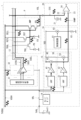
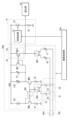
- FIG. 1 is a block diagram illustrating a configuration example of an imaging device according to a first embodiment of the present disclosure.
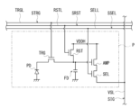
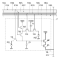
- FIG. 2 is a circuit diagram showing an example of the configuration of the light-receiving pixel shown in FIG.
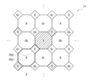
- FIG. 3 is an explanatory diagram showing an example of the arrangement of light-receiving pixels in the pixel array shown in FIG.
- FIG. 4 is a block diagram showing an example of the configuration of the reading section shown in FIG. 1.
- FIG. 5 is a block diagram showing a specific example of the noise correction section shown in FIG. 1.
- FIG. 6 is a circuit diagram showing a specific example of the noise correction section shown in FIG.
- FIG. 7A is an explanatory diagram showing an example of the operation of the noise correction section shown in FIG. 6.
- FIG. 7B is an explanatory diagram showing another example of the operation of the noise correction section shown in FIG. 6.
- FIG. 7C is an explanatory diagram showing another example of the operation of the noise correction section shown in FIG. 6.
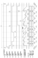
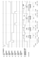
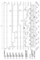
- FIG. 8 is a timing diagram showing an example of the operation of the imaging device shown in FIG.
- FIG. 9 is a timing waveform diagram showing an example of the operation of the imaging device shown in FIG.
- FIG. 10A is an explanatory diagram illustrating an example of noise correction according to the first embodiment.
- FIG. 10B is another explanatory diagram showing an example of noise correction according to the first embodiment.
- FIG. 11 is a characteristic diagram showing an example of the characteristics of the noise removal ratio in the imaging device shown in FIG.
- FIG. 12 is another explanatory diagram showing an example of noise correction according to the first embodiment.
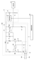
- FIG. 13 is a block diagram illustrating a configuration example of an imaging device according to the second embodiment.
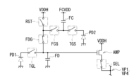
- FIG. 14 is a circuit diagram showing a configuration example of the light-receiving pixel shown in FIG. 13.
- FIG. 15 is an explanatory diagram showing an example arrangement of light-receiving pixels in the pixel array shown in FIG. 13.
- FIG. 16 is a block diagram showing a specific example of the noise correction section shown in FIG. 13.
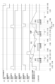
- FIG. 17 is a timing waveform diagram showing an example of the operation of the imaging device shown in FIG. 13.
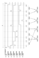
- FIG. 18A is another timing waveform diagram showing an example of the operation of the imaging device shown in FIG. 13.
- FIG. 18B is another timing waveform diagram showing an example of the operation of the imaging device shown in FIG. 13.
- FIG. 18A is another timing waveform diagram showing an example of the operation of the imaging device shown in FIG. 13.
- FIG. 19A is an explanatory diagram showing an example of the operating state of the light-receiving pixel shown in FIG. 14.
- FIG. 19B is an explanatory diagram showing another example of the operating state of the light-receiving pixel shown in FIG. 14.
- FIG. 19C is an explanatory diagram showing another example of the operating state of the light receiving pixel shown in FIG. 14.
- FIG. 20 is an explanatory diagram showing an example of the operation of the signal processing section shown in FIG. 13.
- FIG. 21 is a block diagram illustrating a specific example of a noise correction section according to a modification of the second embodiment.
- FIG. 22 is a circuit diagram showing a specific example of the noise correction section shown in FIG. 21.
- FIG. 23 is a timing waveform diagram illustrating an example of the operation of the imaging device according to a modification of the second embodiment.
- FIG. 24 is a block diagram illustrating a specific example of a noise correction section according to another modification of the second embodiment.
- FIG. 25 is a circuit diagram showing a specific example of the noise correction section shown in FIG. 24.
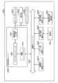
- FIG. 26 is a block diagram showing an example of a schematic configuration of a vehicle control system.
- FIG. 27 is an explanatory diagram showing an example of the installation positions of the outside-vehicle information detection section and the imaging section.
- FIG. 28 is a block diagram illustrating a configuration example of a distance measuring device to which the present technology is applied.
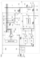
- FIG. 1 shows a configuration example of an imaging device (imaging device 1) according to a first embodiment.
- the imaging device 1 includes a pixel array 11, a drive section 12, a readout section 20, a charge pump 14, a noise correction section 15, a reference signal generation section 16, a signal processing section 17, and an imaging control section 18.
- a pixel array 11 a drive section 12, a readout section 20, a charge pump 14, a noise correction section 15, a reference signal generation section 16, a signal processing section 17, and an imaging control section 18.
- the pixel array 11 has a plurality of light receiving pixels P arranged in a matrix.
- the light-receiving pixel P is configured to generate a pixel signal SIG including a pixel voltage Vpix according to the amount of light received.
- FIG. 2 shows an example of the configuration of the light-receiving pixel P.
- the pixel array 11 includes a plurality of control lines TRGL, a plurality of control lines RSTL, a plurality of control lines SELL, and a plurality of signal lines VSL.
- the control line TRGL extends in the horizontal direction (horizontal direction in FIG. 2), and one end is connected to the drive unit 12.
- a control signal STRG is supplied to the control line TRGL by the drive section 12.
- the control line RSTL extends in the horizontal direction, and one end is connected to the drive unit 12.
- a control signal SRST is supplied to this control line RSTL by the driving section 12.
- the control line SELL extends horizontally, and one end is connected to the drive unit 12.
- a control signal SSEL is supplied to this control line SELL by the drive unit 12.
- the signal line VSL extends in the vertical direction (vertical direction in FIG. 2), and one end is connected to the reading section 20.
- This signal line VSL transmits the pixel signal SIG generated by the light receiving pixel P to the reading unit 20.
- a plurality of light-receiving pixels P arranged in one row in the horizontal direction (horizontal direction in FIGS. 1 and 2) constitute a pixel line L.
- the light receiving pixel P includes a photodiode PD, a transistor TRG, a floating diffusion FD, and transistors RST, AMP, and SEL.
- the transistors TRG, RST, AMP, and SEL are N-type MOS (Metal Oxide Semiconductor) transistors in this example.
- the photodiode PD is a photoelectric conversion element that generates an amount of charge according to the amount of received light and stores the generated charge inside.
- the anode of the photodiode PD is grounded, and the cathode is connected to the source of the transistor TRG.
- the gate of the transistor TRG is connected to the control line TRGL, the source is connected to the cathode of the photodiode PD, and the drain is connected to the floating diffusion FD.
- the floating diffusion FD is configured to accumulate charges transferred from the photodiode PD via the transistor TRG.
- the floating diffusion FD is configured using, for example, a diffusion layer formed on the surface of a semiconductor substrate. In FIG. 2, the floating diffusion FD is shown using a capacitor symbol.
- the gate of the transistor RST is connected to the control line RSTL, the drain is connected to the power supply node of the power supply voltage VDDH, and the source is connected to the floating diffusion FD.
- the gate of the transistor AMP is connected to the floating diffusion FD, the drain is connected to the power supply node of the power supply voltage VDDH, and the source is connected to the drain of the transistor SEL.
- the gate of the transistor SEL is connected to the control line SELL, the drain is connected to the source of the transistor AMP, and the source is connected to the signal line VSL.
- the transistors TRG and RST are turned on based on the control signals STRG and SRST, for example, so that the charges accumulated in the photodiode PD are discharged to the power supply node of the power supply voltage VDDH. . Then, by turning off these transistors TRG and RST, an exposure period T is started, and an amount of charge corresponding to the amount of light received is accumulated in the photodiode PD. After the exposure period T ends, the light receiving pixel P outputs the pixel signal SIG including the reset voltage Vreset and the pixel voltage Vpix to the signal line VSL.
- the transistor SEL is turned on based on the control signal SSEL, so that the light receiving pixel P is electrically connected to the signal line VSL.
- the transistor AMP is connected to a constant current source 21 (described later) of the reading section 20, and operates as a so-called source follower.
- the light-receiving pixel P detects the voltage of the floating diffusion FD at that time during a P-phase (Pre-charge phase) period TP after the voltage of the floating diffusion FD is reset by turning on the transistor RST. A voltage corresponding to the voltage is output as a reset voltage Vreset.
- the light-receiving pixel P responds to the voltage of the floating diffusion FD at that time during the D phase (Data phase) period TD after the charge is transferred from the photodiode PD to the floating diffusion FD by turning on the transistor TRG.
- the resulting voltage is output as the pixel voltage Vpix.
- the voltage difference between the pixel voltage Vpix and the reset voltage Vreset corresponds to the amount of light received by the light receiving pixel P during the exposure period T.
- the light receiving pixel P outputs the pixel signal SIG including the reset voltage Vreset and the pixel voltage Vpix to the signal line VSL.
- FIG. 3 shows an example of the configuration of the pixel array 11.
- unit pixels PP including four light receiving pixels P (light receiving pixels PR, PGr, PGb, PB) are arranged in parallel.
- the light receiving pixel PR has a red (R) color filter and is configured to receive red light.
- the light receiving pixels PGr and PGb have green (G) color filters and are configured to receive green light.
- the light receiving pixel PB has a blue (B) color filter and is configured to receive blue light.
- the light receiving pixel PR is arranged at the upper left
- the light receiving pixel PGr is arranged at the upper right
- the light receiving pixel PGb is arranged at the lower left
- the light receiving pixel PB is arranged at the lower right.
- the four light-receiving pixels PR, PGr, PGb, and PB are arranged in a so-called Bayer array.
- the driving unit 12 (FIG. 1) is configured to sequentially drive the plurality of light-receiving pixels P in the pixel array 11 in units of pixel lines L based on instructions from the imaging control unit 18. Specifically, the drive unit 12 supplies the plurality of control signals STRG to the plurality of control lines TRGL in the pixel array 11, supplies the plurality of control signals SRST to the plurality of control lines RSTL, and supplies the plurality of control signals STRG to the plurality of control lines RSTL. By supplying a plurality of control signals SSEL to SELL, the plurality of light-receiving pixels P in the pixel array 11 are driven in units of pixel lines L. A voltage VRL generated by a charge pump 14 is supplied to the drive unit 12 . The drive unit 12 is configured to drive the plurality of light receiving pixels P using this voltage VRL as a low level voltage of the control signals STRG, SRST, and SSEL.
- the reading unit 20 generates image data DT0 by performing AD conversion based on the pixel signal SIG supplied from the pixel array 11 via the signal line VSL based on an instruction from the imaging control unit 18. configured.
- FIG. 4 shows an example of the configuration of the reading section 20.
- FIG. 4 also depicts the noise correction section 15, the reference signal generation section 16, the signal processing section 17, and the imaging control section 18.
- the reading unit 20 includes a plurality of constant current sources 21, a plurality of AD (Analog to Digital) conversion units ADC, and a transfer control unit 27.
- a plurality of constant current sources 21 and a plurality of AD converters ADC are respectively provided corresponding to the plurality of signal lines VSL.
- the constant current source 21 and the AD converter ADC corresponding to one signal line VSL will be described below.
- the constant current source 21 is configured to cause a predetermined current to flow through the corresponding signal line VSL.
- One end of the constant current source 21 is connected to the corresponding signal line VSL, and the other end is connected to the ground node.
- the AD conversion unit ADC is configured to perform AD conversion based on the pixel signal SIG on the corresponding signal line VSL.
- the AD converter ADC includes capacitors 22 and 23, a comparison circuit 24, a counter 25, and a latch 26.
- the reference signal RAMP supplied from the reference signal generation section 16 is supplied to one end of the capacitor 23 , and the other end is connected to the comparison circuit 24 .
- the reference signal RAMP is a signal having a so-called ramp waveform whose voltage level gradually changes over time.
- the comparison circuit 24 performs a comparison operation based on the pixel signal SIG supplied from the light receiving pixel P via the signal line VSL and the capacitor 22, and the reference signal RAMP supplied from the reference signal generation section 16 via the capacitor 23. and is configured to generate a signal CP by doing so.
- the comparison circuit 24 sets the operating point by setting the voltages of the capacitors 22 and 23 based on the control signal AZSW supplied from the imaging control section 18. After that, the comparison circuit 24 performs a comparison operation of comparing the reset voltage Vreset included in the pixel signal SIG with the voltage of the reference signal RAMP during the P-phase period TP, and compares the reset voltage Vreset included in the pixel signal SIG with the voltage of the reference signal RAMP during the D-phase period TD. A comparison operation is performed to compare the included pixel voltage Vpix and the voltage of the reference signal RAMP.
- the counter 25 is configured to perform a counting operation of counting the pulses of the clock signal CLK supplied from the imaging control section 18 based on the signal CP supplied from the comparison circuit 24. Specifically, the counter 25 counts down the pulses of the clock signal CLK during the P-phase period TP until the signal CP transitions, and counts up the pulses of the clock signal CLK during the D-phase period TD until the signal CP transitions. By counting, a count value CNT is generated. The counter 25 is configured to output this count value CNT as a digital code having a plurality of bits.
- the latch 26 is configured to temporarily hold the digital code supplied from the counter 25 and output the digital code to the bus wiring BUS based on an instruction from the transfer control unit 27.
- the transfer control unit 27 is configured to control the latches 26 of the plurality of AD conversion units ADC to sequentially output digital codes to the bus wiring BUS based on the control signal CTL supplied from the imaging control unit 18. Ru.
- the reading unit 20 uses this bus wiring BUS to sequentially transfer a plurality of digital codes supplied from a plurality of AD conversion units ADC to the signal processing unit 17 as image data DT0.
- Charge pump 14 (FIG. 1) is configured to generate voltage VRL by performing a predetermined pump operation.
- the charge pump 14 is connected to a capacitor Cext1 provided outside the imaging device 1 via a terminal TVRL.
- Voltage VRL is a voltage lower than ground voltage in this example.
- the charge pump 14 generates the voltage VRL by charging and discharging the capacitor Cext1.
- the noise correction unit 15 generates a noise correction signal according to the noise superimposed on the power supply voltage VDDH and a noise correction signal according to the noise superimposed on the voltage VRL based on the instruction from the imaging control unit 18, These noise correction signals are configured to be superimposed on the reference signal RAMP generated by the reference signal generation section 16.
- Power supply voltage VDDH is supplied to imaging device 1 via power supply terminal TVDDH.
- the voltage VRL is generated by the charge pump 14 charging and discharging a capacitor Cext1 provided outside the imaging device 1.
- noise correction section 15 generates noise correction signals according to these noises, and superimposes these generated noise correction signals on the reference signal RAMP generated by the reference signal generation section 16.
- the reference signal generation unit 16 is configured to generate the reference signal RAMP based on instructions from the imaging control unit 18.
- the reference signal RAMP has a so-called ramp waveform in which the voltage level gradually changes over time during the two periods (P-phase period TP and D-phase period TD) in which the reading unit 20 performs AD conversion.
- the reference signal generation section 16 is configured to supply such a reference signal RAMP to the reading section 20.
- FIG. 5 shows an example of the configuration of the drive section 12, the noise correction section 15, and the reference signal generation section 16. Note that, in addition to the driving section 12, the noise correction section 15, and the reference signal generation section 16, the light receiving pixel P, the charge pump 14, and the reading section 20 are also illustrated in FIG.
- the drive section 12 includes a signal generation circuit 31 and a driver section 32.
- the signal generation circuit 31 is configured using, for example, a shift register, and generates a plurality of control signals that are the source of the plurality of control signals STRG, a plurality of control signals that are the source of the plurality of control signals SRST, and a plurality of control signals SSEL. It is configured to generate a plurality of original control signals.
- the driver section 32 has a plurality of drivers.
- the driver section 32 is configured to generate a plurality of control signals STRG, a plurality of control signals SRST, and a plurality of control signals SSEL based on the plurality of control signals supplied from the signal generation circuit 31.
- the driver section 32 is supplied with a power supply voltage VDDH and a voltage VRL.
- the driver section 32 uses the power supply voltage VDDH as a high level voltage and the voltage VRL as a low level voltage to generate control signals STRG, SRST, and SSEL.
- the noise correction section 15 includes a noise correction section 40 and a noise correction section 50.
- the noise correction unit 40 is configured to generate a noise correction signal according to the noise superimposed on the power supply voltage VDDH.
- the noise correction unit 50 is configured to generate a noise correction signal according to the noise superimposed on the voltage VRL.
- the noise correction section 40 includes a high pass filter (HPF) 41, an adjustment circuit 42, and a current source 43.
- the high-pass filter 41 is configured to supply a noise signal, which is an alternating current component, superimposed on the power supply voltage VDDH to the adjustment circuit 42.
- the adjustment circuit 42 is configured to adjust the amplitude and phase of the noise signal supplied from the high-pass filter 41 based on instructions from the imaging control unit 18.
- Current source 43 is configured to convert the noise signal adjusted by adjustment circuit 42 into a current signal.
- the noise correction section 50 includes a high pass filter (HPF) 51, an adjustment circuit 52, and a current source 53.
- the high-pass filter 51 is configured to supply a noise signal, which is an alternating current component, superimposed on the voltage VRL to the adjustment circuit 52.
- the adjustment circuit 52 is configured to adjust the amplitude and phase of the noise signal supplied from the high-pass filter 51 based on instructions from the imaging control unit 18.
- Current source 53 is configured to convert the noise signal adjusted by adjustment circuit 52 into a current signal.
- the noise correction section 15 supplies the current signal generated by the noise correction section 40 to the reference signal generation section 16, thereby superimposing a noise correction signal, which is a voltage signal corresponding to this current signal, on the reference signal RAMP.
- a noise correction signal which is a voltage signal corresponding to this current signal, on the reference signal RAMP.
- the reference signal generation section 16 includes a control circuit 61, a current source 62, and a resistance element 63.
- the control circuit 61 is configured to set the amount of current flowing through the current source 62 based on instructions from the imaging control section 18.
- the current source 62 is connected to the resistance element 63 and is configured to cause a current of an amount according to an instruction from the control circuit 61 to flow through the resistance element 63.
- One end of resistance element 63 is connected to current source 62, and the other end is connected to a ground node.
- a current supplied from the current source 62 flows through the resistance element 63 .
- the reference signal generating section 16 generates a reference signal RAMP which is a voltage signal according to this current.
- a current signal supplied from the noise correction section 15 flows through this resistance element 63.
- a noise correction signal which is a voltage signal corresponding to this current signal, is superimposed on the reference signal RAMP.
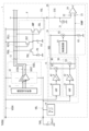
- FIG. 6 shows an example of the configuration of the noise correction section 50. Note that the same applies to the noise correction section 40. In addition to the noise correction section 50, FIG. 6 also depicts the reference signal generation section 16, the imaging control section 78A, and the imaging control section 18.
- the noise correction unit 50 includes a capacitor C1, a resistance element R1, a transistor MN1, a current source CS1, a switch SW1, a resistance element R2, a transistor MN2, a current source CS2, a capacitor C2, and transistors MP1 and MP2. and a capacitor C3.
- Transistors MN1 and MN2 are N-type MOS transistors.
- Transistors MP1 and MP2 are P-type transistors.
- Capacitor C1 corresponds to high pass filter 51 shown in FIG.
- Resistance element R1, transistor MN1, current source CS1, switch SW1, resistance element R2, transistor MN2, current source CS2, capacitor C2, transistor MP1, and capacitor C3 correspond to the adjustment circuit 52 shown in FIG.
- Transistor MP2 corresponds to current source 53 shown in FIG.
- a voltage VRL is supplied to one end of the capacitor C1, and the other end is connected to the switch SW1 and the gate of the transistor MN2.
- One end of resistance element R1 is connected to the source of transistor MN1, and the other end is connected to a ground node.
- the gate of the transistor MN1 is connected to the switch SW1, the drain of the transistor MN1, and the current source CS1, the drain is connected to the current source CS1, the gate of the transistor MN1, and the switch SW1, and the source is connected to one end of the resistive element R1.
- One end of current source CS1 is connected to a power supply node of power supply voltage VDD, and the other end is connected to the drain of transistor MN1, the gate of transistor MN1, and switch SW1.
- One end of the switch SW1 is connected to the gate of the transistor MN1, the drain of the transistor MN1, and the other end of the current source CS1, and the other end is connected to the other end of the capacitor C1 and the gate of the transistor MN2.
- the switch SW1 is turned on and off based on instructions from the imaging control section 18.
- One end of resistance element R2 is connected to the source of transistor MN2, and the other end is connected to a ground node.
- the gate of the transistor MN2 is connected to the other end of the capacitor C1 and the other end of the switch SW1, the drain is connected to the current source CS2, the capacitor C2, the drain of the transistor MP1, and the gates of the transistors MP1 and MP2, and the source is connected to the resistor element R2.
- the current source CS2 is capable of changing the amount of current based on instructions from the imaging control section 18.
- One end of the capacitor C2 is connected to the power supply node of the power supply voltage VDD, and the other end is connected to the drain of the transistor MN2, the other end of the current source CS2, the drain of the transistor MP1, and the gates of the transistors MP1 and MP2.
- the capacitor C2 can change its capacitance value based on instructions from the imaging control section 18.
- the gate of the transistor MP1 is connected to the gate of the transistor MP2, the drain of the transistor MP1, the drain of the transistor MN2, the other end of the current source CS2, and the other end of the capacitor C2, the source is connected to the power supply node of the power supply voltage VDD, and the drain is connected to the gates of transistors MP1 and MP2, the drain of transistor MN2, the other end of current source CS2, and the other end of capacitor C2.
- the gate of transistor MP2 is connected to the gate of transistor MP1, the drains of transistors MP1 and MN2, the other end of current source CS2, and the other end of capacitor C2, its source is connected to the power supply node of power supply voltage VDD, and its drain is connected to the power supply node of power supply voltage VDD.
- the transistor MP2 is configured to be able to change the gate width of the transistor to be operated based on instructions from the imaging control unit 18.
- the voltage VRL is supplied to one end of the capacitor C3, and the other end is connected to the drain of the transistor MP2 and also to the reference signal generation section 16.
- the capacitor C3 is capable of changing its capacitance value based on instructions from the imaging control section 18.
- the noise correction section 50 outputs a current signal according to the noise signal superimposed on the voltage VRL.
- This current signal flows to the resistance element 63 of the reference signal generation section 16.
- a noise correction signal that is a voltage signal corresponding to this current signal is generated.
- the current source CS2, capacitors C2 and C3, and transistor MP2 in the noise correction unit 50 operate based on the adjustment parameters supplied from the imaging control unit 18. Thereby, the adjustment circuit 52 of the noise correction section 50 can adjust the amplitude and phase of the noise correction signal.
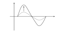
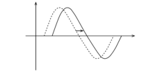
- FIGS. 7A to 7C show an example of the operation of the adjustment circuit 52, with FIG. 7A showing an example of adjusting the amplitude of the noise correction signal, and FIGS. 7B and 7C showing an example of adjusting the phase of the noise correction signal. .
- the adjustment circuit 52 can increase the amplitude of the noise correction signal by increasing the gate width of the transistor MP2 to be operated.
- ⁇ V is the voltage amplitude of the noise signal in transistor MN2.
- Rs is the resistance value of the resistance element R2.
- m is the current mirror ratio in the transistors MP1 and MP2, and indicates the current flowing in the transistor MP2 when the current flowing in the transistor MP1 is "1".
- Ro is the resistance value of the resistance element 63. Therefore, by changing the current mirror ratio, the amplitude of the noise correction signal can be changed.
- the adjustment circuit 52 can delay the phase of the noise correction signal by increasing the capacitance value of the capacitor C2.
- the adjustment circuit 52 can advance the phase of the noise correction signal by increasing the capacitance value of the capacitor C3.
- the signal processing unit 17 (FIG. 1) is configured to generate image data DT by performing predetermined image processing based on the image data DT0 and instructions from the imaging control unit 18.
- the predetermined image processing includes, for example, black level correction processing for correcting the black level, processing for reducing noise, and the like.
- the imaging control section 18 supplies control signals to the driving section 12, the reading section 20, the noise correction section 15, the reference signal generation section 16, and the signal processing section 17, and controls the operation of these circuits, thereby controlling the imaging device. 1. Specifically, the imaging control unit 18 supplies a control signal to the drive unit 12 so that the drive unit 12 sequentially drives the plurality of light receiving pixels P in the pixel array 11 in units of pixel lines L. control. Further, the imaging control unit 18 controls the noise correction unit 15 to adjust, for example, the amplitude and phase of the noise correction signal by supplying a control signal to the noise correction unit 15. Furthermore, the imaging control unit 18 controls the reference signal generation unit 16 to generate the reference signal RAMP by supplying a control signal to the reference signal generation unit 16.
- the imaging control section 18 supplies a control signal to the reading section 20, thereby controlling the reading section 20 to generate image data DT0 by performing AD conversion based on the pixel signal SIG. Further, the imaging control section 18 controls image processing in the signal processing section 17 by supplying a control signal to the signal processing section 17.
- the light-receiving pixel P corresponds to a specific example of a "light-receiving pixel" in an embodiment of the present disclosure.
- the terminal TVRL corresponds to a specific example of a "first connection terminal” in an embodiment of the present disclosure.
- Capacitor Cext1 corresponds to a specific example of a "first external capacitor” in an embodiment of the present disclosure.
- the charge pump 14 corresponds to a specific example of a "first voltage generation circuit” in an embodiment of the present disclosure.
- the drive unit 12 corresponds to a specific example of a "drive circuit” in an embodiment of the present disclosure.
- the reference signal RAMP corresponds to a specific example of a "reference signal” in an embodiment of the present disclosure.
- the reference signal generation unit 16 corresponds to a specific example of a "reference signal generation circuit” in an embodiment of the present disclosure.
- the noise correction unit 50 corresponds to a specific example of a "noise correction circuit” in an embodiment of the present disclosure.
- the comparison circuit 24 corresponds to a specific example of a “comparison circuit” in an embodiment of the present disclosure.
- the counter 25 corresponds to a specific example of a "processing circuit” in an embodiment of the present disclosure.
- the charge pump 14 generates the voltage VRL by charging and discharging a capacitor Cext1 provided outside the imaging device 1.
- the driving section 12 sequentially drives the plurality of light receiving pixels P in the pixel array 11 in units of pixel lines L based on instructions from the imaging control section 18 .
- the reference signal generation unit 16 generates a reference signal RAMP based on instructions from the imaging control unit 18.
- the noise correction unit 15 generates a noise correction signal according to the noise superimposed on the power supply voltage VDDH and a noise correction signal according to the noise superimposed on the voltage VRL based on the instruction from the imaging control unit 18, These generated noise correction signals are superimposed on the reference signal RAMP generated by the reference signal generation section 16.
- the light-receiving pixel P outputs the reset voltage Vreset as the pixel signal SIG during the P-phase period TP, and outputs the pixel voltage Vpix according to the amount of received light as the pixel signal SIG during the D-phase period TD.
- the reading unit 20 reads the image data DT0 based on the pixel signal SIG supplied from the pixel array 11 via the signal line VSL, the reference signal RAMP supplied from the reference signal generation unit 16, and the instruction from the imaging control unit 18. generate. Specifically, in the readout unit 20, the AD conversion unit ADC generates a count value CNT by performing AD conversion based on the pixel signal SIG and the reference signal RAMP, and converts this count value CNT into a plurality of bits. output as a digital code. The reading unit 20 sequentially supplies a plurality of digital codes including the count value CNT generated by the plurality of AD conversion units ADC to the signal processing unit 17 as image data DT0 via the bus wiring BUS. The signal processing unit 17 generates image data DT by performing predetermined image processing based on the image data DT0 and instructions from the imaging control unit 18.
- the plurality of light-receiving pixels P accumulate charges according to the amount of received light, and generate a pixel signal SIG including a pixel voltage Vpix according to the amount of received light. Then, the reading unit 20 performs AD conversion based on this pixel signal SIG and reference signal RAMP. This operation will be explained in detail below.
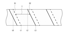
- FIG. 8 shows an example of an operation of scanning a plurality of light-receiving pixels P in the pixel array 11 in units of pixel lines L.
- the imaging device 1 performs exposure start driving D1 on the pixel array 11 in order from the top in the vertical direction.
- the driving unit 12 sequentially selects the pixel lines L by generating control signals STRG and SRST, and sequentially turns on the transistors TRG and RST in the light receiving pixel P for a predetermined length of time. Make it.
- the voltage of the floating diffusion FD and the voltage of the cathode of the photodiode PD are set to the power supply voltage VDDH.
- the photodiode PD starts accumulating charges according to the amount of light received. In this way, the exposure periods T start sequentially in the plurality of light-receiving pixels P.
- the imaging device 1 performs readout drive D2 on the pixel array 11 in the vertical direction from the top in this example.
- the driving unit 12 sequentially selects the pixel lines L by generating control signals STRG, SRST, and SSEL, as described later.
- the light-receiving pixel P outputs the reset voltage Vreset as the pixel signal SIG during the P-phase period TP, and outputs the pixel voltage Vpix as the pixel signal SIG during the D-phase period TD.
- the reading unit 20 performs AD conversion based on the pixel signal SIG output from the light receiving pixel P and including the reset voltage Vreset and the pixel voltage Vpix.
- the imaging device 1 repeats such exposure start drive D1 and readout drive D2. Thereby, the imaging device 1 obtains a series of captured images.
- the read drive D2 will be explained in detail. Focusing on a certain light-receiving pixel P, the operations of this light-receiving pixel P and the AD converter ADC connected to the light-receiving pixel P will be described below.
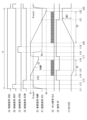
- FIG. 9 shows an example of the operation of the read drive D2, in which (A) shows the waveform of the control signal SSEL, (B) shows the waveform of the control signal SRST, and (C) shows the waveform of the control signal STRG. , (D) shows the waveform of the control signal AZSW, (E) shows the waveform of the reference signal RAMP, (F) shows the waveform of the pixel signal SIG, and (G) shows the waveform of the clock signal CLK. , (H) shows the waveform of the signal CP, and (I) shows the counting operation of the counter 25.
- FIGS. 9E and 9F the waveforms of the reference signal RAMP and the pixel signal SIG are shown using the same voltage axis.
- the waveform of the reference signal RAMP shown in FIG. 9(E) is the waveform of the voltage supplied to the input terminal of the comparator circuit 24 via the capacitor 23, and the waveform of the reference signal RAMP shown in FIG.
- the waveform of the pixel signal SIG is the waveform of the voltage supplied to the input terminal of the comparison circuit 24 via the capacitor 22.
- the horizontal period H starts.
- the drive unit 12 changes the voltage of the control signal SSEL from a low level to a high level (FIG. 9(A)).
- the transistor SEL is turned on, and the light-receiving pixel P is electrically connected to the signal line VSL.
- the drive unit 12 changes the voltage of the control signal SRST from a low level to a high level (FIG. 9(B)).
- the transistor RST is turned on, and the voltage of the floating diffusion FD is set to the power supply voltage VDDH (reset operation).
- the light receiving pixel P outputs a voltage corresponding to the voltage of the floating diffusion FD at this time. Furthermore, at this timing t11, the imaging control unit 18 changes the voltage of the control signal AZSW from a low level to a high level (FIG. 9(D)). Thereby, the comparison circuit 24 of the AD conversion unit ADC sets the operating point by setting the voltages of the capacitors 22 and 23. In this way, the voltage of the pixel signal SIG is set to the reset voltage Vreset, and the voltage of the reference signal RAMP is set to the same voltage as the voltage of the pixel signal SIG (reset voltage Vreset) (Fig. 9(E), ( F)).
- the drive unit 12 changes the voltage of the control signal SRST from a high level to a low level (FIG. 9(B)).
- the transistor RST is turned off, and the reset operation ends.
- the imaging control unit 18 changes the voltage of the control signal AZSW from a high level to a low level (FIG. 9(D)). Thereby, the comparison circuit 24 finishes setting the operating point.
- the reference signal generation unit 16 sets the voltage of the reference signal RAMP to the voltage V1 (FIG. 9(E)).
- the voltage of the reference signal RAMP becomes higher than the voltage of the pixel signal SIG, so the comparison circuit 24 changes the voltage of the signal CP from a low level to a high level ((H) in FIG. 9).
- the AD conversion unit ADC performs AD conversion based on the pixel signal SIG. Specifically, first, at timing t14, the reference signal generation unit 16 starts reducing the voltage of the reference signal RAMP from the voltage V1 by a predetermined degree of change ((E) in FIG. 9). Furthermore, at this timing t14, the imaging control unit 18 starts generating the clock signal CLK (FIG. 9(G)). The counter 25 of the AD conversion unit ADC counts the pulses of the clock signal CLK by performing a down-counting operation (FIG. 9(I)).
- the comparison circuit 24 of the AD conversion unit ADC changes the voltage of the signal CP from a high level to a low level ((H) in FIG. 9).
- the counter 25 of the AD converter ADC stops counting operation based on the transition of the signal CP (FIG. 9(I)).
- the amount of change in the count value between timings t14 and t15 is a value according to the reset voltage Vreset.
- the imaging control unit 18 stops generating the clock signal CLK with the end of the P-phase period TP (FIG. 9(G)). Further, the reference signal generation unit 16 sets the voltage of the reference signal RAMP to the voltage V2 at this timing t16 ((E) in FIG. 9).
- the imaging control unit 18 sets the voltage of the reference signal RAMP to the voltage V1 (FIG. 9(E)).
- the voltage of the reference signal RAMP becomes higher than the voltage of the pixel signal SIG (reset voltage Vreset), so the comparison circuit 24 changes the voltage of the signal CP from a low level to a high level ((H) in FIG. 9).
- the drive unit 12 changes the voltage of the control signal STRG from a low level to a high level (FIG. 9(C)).
- the transistor TRG is turned on, and the charge generated in the photodiode PD is transferred to the floating diffusion FD (charge transfer operation).
- the light receiving pixel P outputs a voltage corresponding to the voltage of the floating diffusion FD at this time. In this way, the voltage of the pixel signal SIG becomes the pixel voltage Vpix (FIG. 9(F)).
- the drive unit 12 changes the voltage of the control signal STRG from a high level to a low level (FIG. 9(C)).
- the transistor TRG is turned off, and the charge transfer operation ends.
- the AD conversion unit ADC performs AD conversion based on the pixel signal SIG. Specifically, first, at timing t20, the reference signal generation unit 16 starts reducing the voltage of the reference signal RAMP from the voltage V1 by a predetermined degree of change ((E) in FIG. 9). Also, at this timing t20, the imaging control unit 18 starts generating the clock signal CLK (FIG. 9(G)). The counter 25 of the AD converter ADC counts the pulses of the clock signal CLK by performing a counting operation by up-counting (FIG. 9(I)).
- the comparison circuit 24 of the AD conversion unit ADC changes the voltage of the signal CP from a high level to a low level ((H) in FIG. 9).
- the counter 25 of the AD converter ADC stops counting operation based on the transition of the signal CP (FIG. 9(I)).
- the amount of change in the count value between timings t20 and t21 is a value that corresponds to the pixel voltage Vpix.
- the latch 26 holds the count value of the counter 25 at this time (count value CNT).
- This count value CNT corresponds to the difference voltage between the pixel voltage Vpix and the reset voltage Vreset, and corresponds to the amount of light received by the light receiving pixel P during the exposure period T.
- the imaging device 1 uses the principle of correlated double sampling (CDS) to obtain a pixel value according to the amount of light received by the light receiving pixel P.
- CDS correlated double sampling
- the imaging control unit 18 stops generating the clock signal CLK with the end of the D-phase period TD ((G) in FIG. 9). Further, the reference signal generation unit 16 sets the voltage of the reference signal RAMP to the voltage V3 at this timing t22 ((E) in FIG. 9). Then, in a period after timing t22, the reading unit 20 supplies the count value CNT held in the latch 26 to the signal processing unit 17 as image data DT0.
- the drive unit 12 changes the voltage of the control signal SSEL from a high level to a low level (FIG. 9(A)).
- the transistor SEL is turned off, and the light-receiving pixel P is electrically disconnected from the signal line VSL.
- the counter 25 resets the count value (FIG. 9(I)).
- the reading unit 20 supplies the image data DT0 including the count value CNT to the signal processing unit 17.
- the signal processing unit 17 generates the image data DT by performing predetermined processing based on, for example, the count value CNT included in the image data DT0.
- the noise correction section 15 generates a noise correction signal according to the noise superimposed on the power supply voltage VDDH and a noise correction signal according to the noise superposed on the voltage VRL, and sends these noise correction signals to the reference signal generation section. 16 is superimposed on the reference signal RAMP generated by the reference signal RAMP. The operations of the noise correction section 50 and the noise correction section 40 will be described in detail below.
- FIGS. 10A and 10B show an example of the operation of the noise correction unit 50
- FIG. 10A shows the operation related to the light receiving pixel P that is the target of the readout drive D2
- FIG. 10B shows the operation related to the light receiving pixel P that is not the target of the readout drive D2.
- the operation related to pixel P is shown.
- the wiring indicated by thick lines indicates the wiring related to the operation of the noise correction unit 50.
- the driver section 32 of the drive section 12 Since the capacitor Cext1 is provided outside the imaging device 1, noise is likely to be superimposed on the voltage VRL.
- the driver section 32 of the drive section 12 generates control signals STRG, SRST, and SSEL by using this voltage VRL as a low-level voltage. Therefore, for example, when the control signal STRG is at a low level, noise is superimposed on the control signal STRG. The same applies to control signals SRST and SSEL.
- the drive unit 12 applies a high-level control signal SSEL and a low-level control signal to the light-receiving pixel P, which is the target of the readout drive D2, during the P-phase period TP and the D-phase period TD. It supplies signals STRG and SRST. Therefore, as shown in FIG. 10A, in this light receiving pixel P, noise corresponding to the noise of the voltage VRL is superimposed on the gate voltages of the transistors TRG and RST. Since the control signal STRG is at a low level, the transistor TRG is in an off state. However, the noise at the gate of transistor TRG is transmitted to the gate of transistor AMP via the parasitic capacitance between the gate and drain of transistor TRG.
- the transistor RST since the control signal SRST is at a low level, the transistor RST is in an off state. However, the noise at the gate of transistor RST is transmitted to the gate of transistor AMP via the parasitic capacitance between the gate and source of transistor RST. Since the control signal SSEL is at a high level, the transistor SEL is in an on state, and the transistor AMP and the constant current source 21 operate as a source follower. Therefore, noise at the gate of transistor AMP is transmitted to signal line VSL. In this way, this light-receiving pixel P outputs a pixel signal SIG on which noise is superimposed.
- the drive unit 12 supplies low-level control signals STRG, SRST, and SSEL to the light-receiving pixels P that are not subject to the readout drive D2. Therefore, as shown in FIG. 10B, in this light-receiving pixel P, noise corresponding to the noise of the voltage VRL is superimposed on the gate voltages of the transistors TRG, RST, and SEL. For example, since the control signal SSEL is at a low level, the transistor SEL is in an off state. However, the noise at the gate of the transistor SEL is transmitted to the source of the transistor SEL via the parasitic capacitance between the gate and source of the transistor SEL. Therefore, this light-receiving pixel P superimposes noise on the pixel signal SIG generated by the light-receiving pixel P that is the target of the readout drive D2.
- the pixel signal SIG on which noise is superimposed is supplied to the comparison circuit 24 via the capacitor 22.
- the noise correction section 50 generates a noise correction signal according to the noise superimposed on the voltage VRL, and converts this noise correction signal into the reference signal RAMP generated by the reference signal generation section 16. superimpose on The reference signal RAMP on which the noise correction signal has been superimposed is supplied to the comparison circuit 24 via the capacitor 23.
- the amplitude and phase of the noise correction signal are adjusted in advance to be approximately the same as the amplitude and phase of the noise superimposed on the pixel signal SIG.
- the pixel signal SIG and the reference signal RAMP supplied to the comparison circuit 24 are superimposed with noise and noise correction signals that are in phase with each other.
- the comparison circuit 24 Since the comparison circuit 24 operates based on the difference between the two supplied signals, the influence of noise on the signal CP generated by the comparison circuit 24 can be suppressed. As a result, in the imaging device 1, the influence of noise of the voltage VRL on the captured image can be suppressed.
- the comparison circuit 24 performs a comparison operation based on the pixel signal SIG on which noise is superimposed and the reference signal RAMP on which no noise correction signal is superimposed.
- the noise of the voltage VRL affects the captured image. For example, since the same noise is superimposed on the pixel signals SIG output from the plurality of light-receiving pixels P belonging to the pixel line L, horizontal streaks depending on the noise may appear in the captured image.
- the imaging device 1 since the imaging device 1 is provided with the noise correction section 50, the in-phase noise and noise correction signal are superimposed on the pixel signal SIG and the reference signal RAMP supplied to the comparison circuit 24, respectively. Thereby, in the imaging device 1, the influence of noise of the voltage VRL on the captured image can be suppressed.
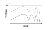
- FIG. 11 shows an example of the characteristics of the noise removal ratio for noise superimposed on the voltage VRL, where the horizontal axis shows the frequency and the vertical axis shows the noise removal ratio.
- the noise removal ratio is the ratio between the noise voltage superimposed on the voltage VRL and the value obtained by converting the pixel value in the captured image into voltage, and the smaller the value, the more noise is removed.
- the solid line indicates the characteristics of the imaging device 1 according to the present embodiment, and the broken line indicates the characteristics of the imaging device when the noise correction section 50 is not provided. In the imaging device 1, since the noise correction section 50 is provided, the noise removal ratio can be reduced.
- FIG. 12 shows an example of the operation of the noise correction section 40.
- FIG. 12 shows the operation related to the light-receiving pixel P that is the target of the readout drive D2.
- the wiring indicated by thick lines indicates the wiring related to the operation of the noise correction section 40.
- the driver section 32 of the drive section 12 Since the power supply voltage VDDH is supplied from outside the imaging device 1, noise is likely to be superimposed on the power supply voltage VDDH.
- the driver section 32 of the drive section 12 generates control signals STRG, SRST, and SSEL by using this power supply voltage VDDH as a high-level voltage. Therefore, for example, when the control signal SSEL is at a high level, noise is superimposed on the control signal SSEL.
- the drive unit 12 applies a high-level control signal SSEL and a low-level control signal to the light-receiving pixel P, which is the target of the readout drive D2, during the P-phase period TP and the D-phase period TD. It supplies signals STRG and SRST. Therefore, as shown in FIG. 12, in this light receiving pixel P, noise corresponding to the noise of the power supply voltage VDDH is superimposed on the gate voltage of the transistor SEL. Furthermore, in the light receiving pixel P, noise corresponding to the noise of the power supply voltage VDDH is superimposed on the gate voltage of the transistor AMP via the parasitic capacitance between the power supply wiring of the power supply voltage VDDH and the floating diffusion FD.
- control signal SSEL is at a high level
- the transistor SEL is in an on state
- the transistor AMP and the constant current source 21 operate as a source follower.
- the power supply voltage VDDH on which noise is superimposed is supplied to the drain of the transistor AMP.
- the noise correction section 40 generates a noise correction signal according to the noise superimposed on the power supply voltage VDDH, and superimposes this noise correction signal on the reference signal RAMP generated by the reference signal generation section 16.
- the reference signal RAMP on which the noise correction signal has been superimposed is supplied to the comparison circuit 24 via the capacitor 23.
- the amplitude and phase of the noise correction signal are adjusted in advance to be approximately the same as the amplitude and phase of the noise superimposed on the pixel signal SIG.
- the pixel signal SIG and the reference signal RAMP supplied to the comparison circuit 24 are superimposed with noise and noise correction signals that are in phase with each other.
- the characteristics of the noise removal ratio are similar to those of the noise correction section 50 (FIG. 11).
- the imaging device 1 includes a light-receiving pixel P capable of generating a pixel signal SIG including a pixel voltage Vpix corresponding to the amount of received light, a terminal TVRL connected to the capacitor Cext1, and a charger capable of generating a voltage at the terminal TVRL.
- a pump 14 a driving section 12 capable of driving the light receiving pixel P based on the voltage at the terminal TVRL, a reference signal generating section 16 capable of generating a reference signal RAMP having a ramp waveform, and noise correction according to the voltage at the terminal TVRL.
- a noise correction unit 50 that can generate a signal and superimpose a noise correction signal on the reference signal RAMP, a comparison circuit 24 that can compare the pixel signal SIG and the reference signal RAMP on which the noise correction signal is superimposed, A signal processing section 17 capable of calculating pixel values based on the comparison results of the circuit 24 is provided.
- the pixel signal SIG and the reference signal RAMP supplied to the comparison circuit 24 are superimposed with noise and noise correction signals that are in phase with each other, so that the influence of the noise of the voltage VRL on the captured image is suppressed. be able to.
- a light-receiving pixel capable of generating a pixel signal including a pixel voltage according to the amount of light, a terminal connected to a capacitor, a charge pump capable of generating a voltage at the terminal, and a voltage at the terminal are provided.
- a driving section that can drive the light-receiving pixel based on the reference signal
- a reference signal generating section that can generate a reference signal having a ramp waveform
- a noise correction signal that can generate a noise correction signal according to the voltage at the terminal, and the noise correction signal as the reference signal.
- noise correction unit that can be superimposed on the noise correction signal
- comparison circuit that can compare the pixel signal and a reference signal on which the noise correction signal is superimposed
- signal processing unit that can calculate the pixel value based on the comparison result of the comparison circuit. Since this is provided, the influence of noise can be suppressed.
- an imaging device 2 according to a second embodiment will be described.
- This embodiment is an example in which the circuit configuration of the light receiving pixel P is changed and two external capacitors are provided. Components that are substantially the same as those of the imaging device 1 according to the first embodiment are given the same reference numerals, and description thereof will be omitted as appropriate.
- FIG. 13 shows an example of the configuration of the imaging device 2 according to the second embodiment.
- the imaging device 2 includes a pixel array 71, a drive section 72, a bias circuit 74, a noise correction section 75, a signal processing section 77, and an imaging control section 78.
- the pixel array 71 includes a plurality of light-receiving pixels P arranged in a matrix.
- FIG. 14 shows an example of the configuration of the light-receiving pixel P.
- the pixel array 71 includes a plurality of control lines TGLL, a plurality of control lines FDGL, a plurality of control lines RSTL, a plurality of control lines FCGL, a plurality of control lines TGSL, a plurality of control lines SELL, and a plurality of signals. line VSL.
- the control line TGLL extends in the horizontal direction (horizontal direction in FIG. 14), and one end is connected to the drive unit 72.
- a control signal STGL is supplied to this control line TGLL by the driving section 72.
- the control line FDGL extends in the horizontal direction, and one end is connected to the drive unit 72.
- a control signal SFDG is supplied to this control line FDGL by the drive section 72.
- the control line RSTL extends in the horizontal direction, and one end is connected to the drive unit 72.
- a control signal SRST is supplied to this control line RSTL by the driving section 72.
- the control line FCGL extends in the horizontal direction, and one end is connected to the drive unit 72.
- a control signal SFCG is supplied to this control line FCGL by the drive unit 72.
- the control line TGSL extends in the horizontal direction, and one end is connected to the drive unit 72.
- a control signal STGS is supplied to this control line TGSL by the driving section 72.
- the control line SELL extends horizontally, and one end is connected to the drive unit 72.
- a control signal SSEL is supplied to the control line SELL by the drive unit 72.
- the light receiving pixel P includes a photodiode PD1, a transistor TGL, a photodiode PD2, a transistor TGS, a capacitor FC, a transistor FCG, RST, FDG, a floating diffusion FD, and a transistor AMP, SEL. .
- the transistors TGL, TGS, FCG, RST, FDG, AMP, and SEL are N-type MOS transistors in this example.
- the photodiode PD1 is a photoelectric conversion element that generates an amount of charge according to the amount of received light and stores the generated charge inside.
- the light receiving area where the photodiode PD1 can receive light is wider than the light receiving area where the photodiode PD2 can receive light.
- the anode of the photodiode PD1 is grounded, and the cathode is connected to the source of the transistor TGL.
- the gate of the transistor TGL is connected to the control line TGLL, the source is connected to the cathode of the photodiode PD1, and the drain is connected to the floating diffusion FD.
- the photodiode PD2 is a photoelectric conversion element that generates an amount of charge according to the amount of received light and stores the generated charge inside.
- the light receiving area where the photodiode PD2 can receive light is narrower than the light receiving area where the photodiode PD1 can receive light.
- the anode of the photodiode PD2 is grounded, and the cathode is connected to the source of the transistor TGS.
- the gate of the transistor TGS is connected to the control line TGSL, the source is connected to the cathode of the photodiode PD2, and the drain is connected to the capacitor FC and the source of the transistor FCG.
- One end of the capacitor FC is connected to the drain of the transistor TGS and the source of the transistor FCG, and the other end is supplied with the control signal FCVDD.
- the gate of the transistor FCG is connected to the control line FCGL, the source is connected to one end of the capacitor FC and the drain of the transistor TGS, and the drain is connected to the source of the transistor RST and the drain of the transistor FDG.
- the gate of the transistor RST is connected to the control line RSTL, the drain is supplied with the power supply voltage VDDH, and the source is connected to the drains of the transistors FCG and FDG.
- the gate of the transistor FDG is connected to the control line FDGL, the drain is connected to the source of the transistor RST and the drain of the transistor FCG, and the source is connected to the floating diffusion FD.
- the floating diffusion FD is configured to accumulate charges supplied from the photodiodes PD1 and PD2.
- the floating diffusion FD is configured using, for example, a diffusion layer formed on the surface of a semiconductor substrate. In FIG. 14, the floating diffusion FD is shown using a capacitor symbol.
- the transistor SEL is turned on based on the control signal SSEL, so that the light receiving pixel P is electrically connected to the signal line VSL.
- the transistor AMP is connected to the constant current source 21 of the reading section 20 and operates as a so-called source follower.
- the light-receiving pixel P outputs a pixel voltage VP corresponding to the voltage at the floating diffusion FD to the signal line VSL as a pixel signal SIG.
- the light-receiving pixel P sequentially outputs eight pixel voltages VP (VP1 to VP8) in eight periods (conversion periods T1 to T8) within the so-called horizontal period H. ing.
- FIG. 15 shows an example of the arrangement of photodiodes PD1 and PD2 in the pixel array 71.
- "R” indicates a red color filter
- "Gr” and “Gb” indicate a green color filter
- "B” indicates a blue color filter.
- a photodiode PD2 is formed to the upper right of the photodiode PD1.
- Color filters of the same color are formed in the two photodiodes PD1 and PD2 in each light-receiving pixel P.
- photodiode PD1 has an octagonal shape
- photodiode PD2 has a quadrangular shape. As shown in this figure, the light receiving area where the photodiode PD1 can receive light is wider than the light receiving area where the photodiode PD2 can receive light.
- the driving unit 72 (FIG. 13) is configured to sequentially drive the plurality of light-receiving pixels P in the pixel array 71 in units of pixel lines L based on instructions from the imaging control unit 78. Specifically, the drive unit 72 supplies the plurality of control signals STGL to the plurality of control lines TGLL in the pixel array 71, respectively supplies the plurality of control signals SFDG to the plurality of control lines FDGL, and supplies the plurality of control signals STGL to the plurality of control lines FDGL.
- a plurality of control signals SRST are respectively supplied to RSTL, a plurality of control signals SFCG are respectively supplied to a plurality of control lines FCGL, a plurality of control signals STGS are respectively supplied to a plurality of control lines TGSL, and a plurality of control signals SELL are supplied to a plurality of control lines SELL.
- a plurality of control signals SSEL By respectively supplying a plurality of control signals SSEL, a plurality of light receiving pixels P in the pixel array 71 are driven in units of pixel lines L.
- the drive unit 72 supplies the control signal FCVDD to the plurality of light receiving pixels P in the pixel array 71.
- the drive unit 72 is supplied with the voltage VRL generated by the charge pump 14 and also supplied with the voltage VRH generated by the bias circuit 74.
- Bias circuit 74 is configured to generate voltage VRH.
- the bias circuit 74 is connected to a capacitor Cext2 provided outside the imaging device 2 via a terminal TVRH.
- voltage VRH is higher than the ground voltage and lower than power supply voltage VDDH.
- the bias circuit 74 is provided in this example, the present invention is not limited to this, and instead, for example, a charge pump may be provided. In this case, for example, voltage VRH can be made higher than power supply voltage VDDH.
- the noise correction unit 75 Based on instructions from the imaging control unit 78, the noise correction unit 75 generates a noise correction signal corresponding to the noise superimposed on the power supply voltage VDDH, a noise correction signal corresponding to the noise superimposed on the voltage VRL, and a noise correction signal corresponding to the noise superimposed on the voltage VRH. It is configured to generate noise correction signals according to the superimposed noise and to superimpose these noise correction signals on the reference signal RAMP generated by the reference signal generation section 16.
- FIG. 16 shows a specific example of the drive section 72 and the noise correction section 75. Note that, in addition to the drive section 72 and the noise correction section 75, FIG. 16 also depicts the light receiving pixel P, the charge pump 14, the bias circuit 74, the reference signal generation section 16, and the readout section 20.
- the drive section 72 includes a signal generation circuit 81, a driver section 82, and a driver 83.
- the signal generation circuit 81 is configured using, for example, a shift register, and generates a plurality of control signals that are the sources of the plurality of control signals STGL, a plurality of control signals that are the sources of the plurality of control signals SFDG, and a plurality of control signals that are the sources of the plurality of control signals SRST. , a plurality of control signals which are the source of the plurality of control signals SFCG, a plurality of control signals which are the source of the plurality of control signals STSG, and a plurality of control signals which are the source of the plurality of control signals SSEL. configured to generate.
- the signal generation circuit 81 also has a function of generating a control signal that becomes the basis of the control signal SFCVDD.
- the driver section 82 has a plurality of drivers.
- the driver unit 82 generates a plurality of control signals STGL, a plurality of control signals SFDG, a plurality of control signals SRST, a plurality of control signals SFCG, and a plurality of control signals STSG based on the plurality of control signals supplied from the signal generation circuit 81. , and a plurality of control signals SSEL.
- the driver section 82 is supplied with a power supply voltage VDDH and a voltage VRL.
- the driver section 82 uses the power supply voltage VDDH as a high level voltage and the voltage VRL as a low level voltage to generate control signals STGL, SFDG, SRST, SFCG, STGS, and SSEL.
- the driver 83 is configured to generate the control signal SFCVDD based on the control signal supplied from the signal generation circuit 81.
- a voltage VRH is supplied to the driver 83.
- the driver 83 is configured to output this voltage VRH as a control signal SFCVDD.
- the noise correction section 75 has a noise correction section 90.
- the noise correction unit 90 is configured to generate a noise correction signal according to the noise superimposed on the voltage VRL and a noise correction signal according to the noise superimposed on the voltage VRH.
- the noise correction section 90 includes a high pass filter (HPF) 91, an adjustment circuit 92, a current source 93, a high pass filter (HPF) 94, an adjustment circuit 95, and a current source 96.
- High-pass filter 91 is configured to supply a noise signal, which is an alternating current component, superimposed on voltage VRH to adjustment circuit 92 .
- the adjustment circuit 92 is configured to adjust the amplitude and phase of the noise signal supplied from the high-pass filter 91 based on instructions from the imaging control section 78.
- Current source 93 is configured to convert the noise signal adjusted by adjustment circuit 92 into a current signal.
- High-pass filter 94 is configured to supply a noise signal, which is an alternating current component, superimposed on voltage VRL to adjustment circuit 95 .
- the adjustment circuit 95 is configured to adjust the amplitude and phase of the noise signal supplied from the high-pass filter 94 based on instructions from the imaging control unit 78.
- Current source 96 is configured to convert the noise signal adjusted by adjustment circuit 95 into a current signal.
- Each of the high-pass filters 91 and 94 has the same circuit configuration as the high-pass filter 51 (FIG. 6) according to the first embodiment.
- Each of the adjustment circuits 92 and 95 has the same circuit configuration as the adjustment circuit 52 (FIG. 6) according to the first embodiment.
- Each of current sources 93 and 96 has the same circuit configuration as current source 53 (FIG. 6) according to the first embodiment.
- the signal processing unit 77 (FIG. 13) is configured to generate image data DT by performing predetermined image processing based on the image data DT0 and instructions from the imaging control unit 78.
- the imaging control section 78 supplies control signals to the driving section 72, the reading section 20, the noise correction section 75, the reference signal generation section 16, and the signal processing section 77, and controls the operation of these circuits to control the imaging apparatus. 2.
- the terminal TVRH corresponds to a specific example of a "second connection terminal” in an embodiment of the present disclosure.
- Capacitor Cext2 corresponds to a specific example of a “second external capacitor” in an embodiment of the present disclosure.
- the bias circuit 74 corresponds to a specific example of a "second voltage generation circuit” in an embodiment of the present disclosure.
- the imaging control unit 78 corresponds to a specific example of a "control circuit" in an embodiment of the present disclosure.
- the read drive D2 will be explained in detail. Focusing on a certain light-receiving pixel P, the operations of this light-receiving pixel P and the AD converter ADC connected to the light-receiving pixel P will be described below.
- 17, 18A, and 18B represent an example of the operation of the imaging device 2.
- 17, 18A, and 18B (A) shows the waveform of the horizontal synchronization signal XHS, (B) shows the waveform of the control signal SSEL, (C) shows the waveform of the control signal SRST, and (D) shows the waveform of the control signal (E) shows the waveform of the control signal STGL, (F) shows the waveform of the control signal SFCG, (G) shows the waveform of the control signal STGS, (H) shows the waveform of the control signal STGS, and (H) shows the waveform of the control signal STGS. (I) shows the waveform of the pixel signal SIG, and (J) shows the operation of the counter 25.
- FIG. 17 shows an adjustment parameter related to the voltage VRL in the noise correction section 90
- (L) shows an adjustment parameter related to the voltage VRH in the noise correction section 90
- 18A shows the first half of the operations shown in FIG. 17, and
- FIG. 18B shows the second half of the operations shown in FIG. 17.
- diagonal lines indicate that the counter 25 is performing a counting operation.
- FIGS. 19A to 19C represent the states of the light-receiving pixels P.
- transistors TGL, RST, FDG, TGS, FCG, and SEL are each shown using a switch depending on the operating state of the transistor.
- the drive unit 72 changes the voltage of the control signal SSEL from a low level to a high level at timing t102 (FIG. 18A(B)).
- the transistor SEL is turned on, and the light-receiving pixel P is electrically connected to the signal line VSL.
- the drive unit 72 sets both the control signals SRST and SFDG to high level (FIGS. 18A(C) and (D)).
- both transistors RST and FDG are turned on, the voltage of the floating diffusion FD is set to the power supply voltage VDDH, and the floating diffusion FD is reset.
- the drive unit 72 changes the voltage of the control signal SFDG from a high level to a low level (FIG. 18A(D)). As a result, in the light receiving pixel P, the transistor FDG is turned off.
- the drive unit 72 changes the voltage of the control signal SRST from a high level to a low level (FIG. 18A(C)). As a result, in the light receiving pixel P, the transistor RST is turned off.
- the drive unit 72 changes the voltage of the control signal SFDG from a low level to a high level (FIG. 18A(D)). As a result, in the light-receiving pixel P, the transistor FDG is turned on.
- the comparison circuit 24 sets the operating point based on the control signal AZSW during the period from timing t113 to t114.
- the comparison circuit 24 finishes setting the operating point. Then, at this timing t114, the reference signal generation unit 16 changes the voltage of the reference signal RAMP to the voltage V1 (FIG. 18A(H)).
- the transistors FDG and SEL are turned on, and all other transistors are turned off. Since transistor FDG is in the on state, floating diffusion FD and transistor FDG constitute a composite capacitance. This composite capacitance functions as a conversion capacitance that converts charge into voltage in the light-receiving pixel P. In the light-receiving pixel P, since the transistor FDG is in the on state, the conversion capacitance in the light-receiving pixel P is large, and the conversion efficiency from charge to voltage is low. This conversion capacitance holds the charge when the floating diffusion FD is reset during the period up to timing t112. The light receiving pixel P outputs a pixel voltage VP (pixel voltage VP1) according to the voltage at the floating diffusion FD at this time.
- a pixel voltage VP pixel voltage VP1
- the AD conversion unit ADC performs AD conversion based on this pixel voltage VP1. Specifically, at timing t115, the imaging control unit 78 starts generating the clock signal CLK, and at the same time, the reference signal generation unit 16 changes the voltage of the reference signal RAMP from the voltage V1 by a predetermined degree of change. It starts to decrease (FIG. 18A(H)). In response to this, the counter 25 of the AD converter ADC starts counting operation (FIG. 18A(J)). In this example, the counter 25 always counts the pulses of the clock signal CLK by up-counting.
- the voltage of the reference signal RAMP becomes lower than the voltage of the pixel signal SIG (pixel voltage VP1) (FIGS. 18A (H) and (I)).
- the comparison circuit 24 of the AD converter ADC changes the voltage of the signal CP, and as a result, the counter 25 stops counting (FIG. 18A(J)).
- the count value CNT of the counter 25 when the counting operation is stopped corresponds to the pixel voltage VP1.
- the AD conversion unit ADC thus performs AD conversion based on the pixel voltage VP1, and the latch 26 of the AD conversion unit ADC holds the count value CNT of the counter 25 and converts the held count value CNT into a digital code. Output as CODE1 (FIG. 18A(J)).
- the imaging control unit 78 stops generating the clock signal CLK with the end of the conversion period T1
- the reference signal generation unit 16 stops changing the voltage of the reference signal RAMP (FIG. 18A ( H))
- the counter 25 resets the count value CNT.
- the drive unit 72 changes the voltage of the control signal SFDG from a high level to a low level (FIG. 18A(D)).
- the transistor FDG is turned off.
- the comparison circuit 24 sets the operating point based on the control signal AZSW during the period from timing t121 to timing t122.
- the comparison circuit 24 finishes setting the operating point. Then, at this timing t122, the reference signal generation unit 16 changes the voltage of the reference signal RAMP to the voltage V1 (FIG. 18A(H)).
- the transistor SEL is turned on, and all other transistors are turned off.
- the conversion capacitance in the light-receiving pixel P is small, so that the conversion efficiency from charge to voltage is high. This conversion capacitance holds the charge when the floating diffusion FD is reset during the period up to timing t112.
- the light receiving pixel P outputs a pixel voltage VP (pixel voltage VP2) according to the voltage at the floating diffusion FD at this time.
- the AD conversion unit ADC performs AD conversion based on this pixel voltage VP2. This operation is similar to the operation during the conversion period T1.
- the AD converter ADC performs AD conversion based on the pixel voltage VP2, and the latch 26 of the AD converter ADC holds the count value CNT of the counter 25 and outputs the held count value CNT as a digital code CODE2 ( Figure 18A(J)).
- the drive unit 72 changes the voltage of the control signal STGL from a low level to a high level (FIG. 18A(E)).
- the transistor TGL is turned on, and the charge generated in the photodiode PD1 is transferred to the floating diffusion FD.
- the reference signal generation unit 16 changes the voltage of the reference signal RAMP to the voltage V1 (FIG. 18A(H)).
- the drive unit 72 changes the voltage of the control signal STGL from a high level to a low level (FIG. 18A(E)). As a result, in the light-receiving pixel P, the transistor TGL is turned off.
- the conversion capacitance in the light-receiving pixel P is small, so the conversion efficiency from charge to voltage is high.
- This conversion capacitance holds the charges transferred from the photodiode PD1 at timings t131 to t132.
- the light receiving pixel P outputs a pixel voltage VP (pixel voltage VP3) according to the voltage at the floating diffusion FD at this time.
- the AD conversion unit ADC performs AD conversion based on this pixel voltage VP3. This operation is similar to the operation during the conversion period T1.
- the AD converter ADC performs AD conversion based on the pixel voltage VP3, and the latch 26 of the AD converter ADC holds the count value CNT of the counter 25 and outputs the held count value CNT as a digital code CODE3 ( Figure 18A(J)).
- This digital code CODE3 corresponds to the digital code CODE2 obtained when the conversion efficiency is also high (conversion period T2).
- the drive unit 72 changes the voltage of the control signal SFDG from a low level to a high level, and changes the voltage of the control signal STGL from a low level to a high level (FIGS. 18A(D), (E) )). As a result, in the light-receiving pixel P, both transistors FDG and TGL are turned on. Further, at this timing t141, the reference signal generation unit 16 changes the voltage of the reference signal RAMP to the voltage V1 (FIG. 18A(H)). Next, the drive unit 72 changes the voltage of the control signal STGL from a high level to a low level at timing t142 (FIG. 18A(E)). As a result, in the light-receiving pixel P, the transistor TGL is turned off.
- the transistor FDG is in the on state, so the floating diffusion FD and the transistor FDG constitute a composite capacitance (conversion capacitance). Therefore, since the conversion capacitance in the light-receiving pixel P is large, the conversion efficiency from charge to voltage is low. This conversion capacitance holds charges transferred from the photodiode PD1 at timings t131 to t132 and t141 to t142.
- the light-receiving pixel P outputs a pixel voltage VP (pixel voltage VP4) according to the voltage at the floating diffusion FD at this time.
- the AD conversion unit ADC performs AD conversion based on this pixel voltage VP4. This operation is similar to the operation during the conversion period T1.
- the AD converter ADC performs AD conversion based on the pixel voltage VP4, and the latch 26 of the AD converter ADC holds the count value CNT of the counter 25 and outputs the held count value CNT as a digital code CODE4 ( Figure 18A(J)).
- This digital code CODE4 corresponds to the digital code CODE1 obtained when the conversion efficiency is also low (conversion period T1).
- the drive unit 72 changes the voltage of the control signal SRST from a low level to a high level (FIG. 18B(C)).
- the transistor RST is turned on. Since the transistor FDG is in the on state, the voltage of the floating diffusion FD is thereby set to the power supply voltage VDDH, and the floating diffusion FD is reset.
- the drive unit 72 changes the voltage of the control signal SRST from a high level to a low level (FIG. 18B(C)). As a result, in the light receiving pixel P, the transistor RST is turned off.
- the reference signal generation unit 16 changes the voltage of the reference signal RAMP to the voltage V1 (FIG. 18B(H)).
- the drive unit 72 changes the voltage of the control signal SFCG from a low level to a high level (FIG. 18B(F)).
- the transistor FCG is turned on.
- the comparison circuit 24 sets the operating point based on the control signal AZSW during the period from timing t153 to timing t154.
- the comparison circuit 24 finishes setting the operating point. Further, at this timing t154, the reference signal generation unit 16 changes the voltage of the reference signal RAMP to the voltage V1 (FIG. 18A(H)).
- the transistors FDG, FCG, and SEL are turned on, and all other transistors are turned off. Since transistors FDG and FCG are both in the on state, floating diffusion FD, transistors FDG and FCG, and capacitor FC constitute a composite capacitance (conversion capacitance). This conversion capacitance holds the charge generated in the photodiode PD2 before timing t153, supplied to the capacitor FC via the transistor TGS, and stored.
- the light-receiving pixel P outputs a pixel voltage VP (pixel voltage VP5) according to the voltage at the floating diffusion FD at this time.
- the AD conversion unit ADC performs AD conversion based on this pixel voltage VP5. This operation is similar to the operation during the conversion period T1.
- the AD converter ADC performs AD conversion based on the pixel voltage VP5, and the latch 26 of the AD converter ADC holds the count value CNT of the counter 25 and outputs the held count value CNT as a digital code CODE5 ( Figure 18B(J)).
- the drive unit 72 changes the voltage of the control signal STGS from a low level to a high level (FIG. 18B(G)).
- the transistor TGS is turned on.
- the reference signal generation unit 16 changes the voltage of the reference signal RAMP to the voltage V1 (FIG. 18B(H)).
- the drive unit 72 changes the voltage of the control signal STGS from a high level to a low level (FIG. 18B(G)). As a result, in the light-receiving pixel P, the transistor TGS is turned off.
- the floating diffusion FD, the transistors FDG and FCG, and the capacitor FC constitute a composite capacitance (conversion capacitance).
- This conversion capacitance holds the charge transferred from the photodiode PD2 between timings t161 and t162 in addition to the charge that was generated in the photodiode PD2 before timing t53, and was supplied to and stored in the capacitor FC via the transistor TGS. are doing.
- the light receiving pixel P outputs a pixel voltage VP (pixel voltage VP6) according to the voltage at the floating diffusion FD at this time.
- the AD conversion unit ADC performs AD conversion based on this pixel voltage VP6. This operation is similar to the operation during the conversion period T1.
- the AD converter ADC performs AD conversion based on the pixel voltage VP6, and the latch 26 of the AD converter ADC holds the count value CNT of the counter 25 and outputs the held count value CNT as a digital code CODE6 ( Figure 18B(J)).
- This digital code CODE6 corresponds to the digital code CODE5 obtained when the floating diffusion FD, transistors FDG, FCG, and capacitor FC constitute a composite capacitance.
- the comparison circuit 24 sets the operating point based on the control signal AZSW during the period from timing t171 to timing t172.
- the comparison circuit 24 finishes setting the operating point and electrically disconnects the positive input terminal and the negative input terminal. Further, at this timing t72, the reference signal generation unit 16 changes the voltage of the reference signal RAMP to the voltage V1 (FIG. 18B(H)).
- the floating diffusion FD, the transistors FDG and FCG, and the capacitor FC constitute a composite capacitance (conversion capacitance).
- This conversion capacitance holds the charge transferred from the photodiode PD2 between timings t161 and t162, in addition to the charge that was generated in the photodiode PD2 before timing t153, and was supplied to and stored in the capacitor FC via the transistor TGS. are doing.
- the light-receiving pixel P outputs a pixel voltage VP (pixel voltage VP7) according to the voltage at the floating diffusion FD at this time.
- the AD conversion unit ADC performs AD conversion based on this pixel voltage VP7. This operation is similar to the operation during the conversion period T1.
- the AD converter ADC performs AD conversion based on the pixel voltage VP7, and the latch 26 of the AD converter ADC holds the count value CNT of the counter 25 and outputs the held count value CNT as a digital code CODE7 ( Figure 18B(J)).
- the drive unit 72 changes the voltage of the control signal SRST from a low level to a high level (FIG. 18B(C)).
- the transistor RST is turned on. Since transistors FDG and FCG are in the on state, the voltage of floating diffusion FD and the voltage of capacitor FC are set to power supply voltage VDDH, and floating diffusion FD and capacitor FC are reset.
- the drive unit 72 changes the voltage of the control signal SFCG from a high level to a low level (FIG. 18B(F)). As a result, in the light-receiving pixel P, the transistor FCG is turned off.
- the drive unit 72 changes the voltage of the control signal SRST from a high level to a low level (FIG. 18B(C)). As a result, in the light receiving pixel P, the transistor RST is turned off.
- the drive unit 72 changes the voltage of the control signal SFCG from a low level to a high level (FIG. 18B(F)).
- the transistor FCG is turned on.
- the reference signal generation unit 16 changes the voltage of the reference signal RAMP to the voltage V1 (FIG. 18B(H)).
- the floating diffusion FD, the transistors FDG and FCG, and the capacitor FC constitute a composite capacitance (conversion capacitance).
- This conversion capacitance holds the charge when the floating diffusion FD and capacitor FC are reset at timings t181 to t182.
- the light-receiving pixel P outputs a pixel voltage VP (pixel voltage VP8) according to the voltage at the floating diffusion FD at this time.
- the AD conversion unit ADC performs AD conversion based on this pixel voltage VP8. This operation is similar to the operation during the conversion period T1.
- the AD converter ADC performs AD conversion based on the pixel voltage VP8, and the latch 26 of the AD converter ADC holds the count value CNT of the counter 25 and outputs the held count value CNT as a digital code CODE8 ( Figure 18B(J)).
- This digital code CODE8 corresponds to the digital code CODE7 obtained when the floating diffusion FD, transistors FDG, FCG, and capacitor FC constitute a composite capacitance.
- the drive unit 72 changes the voltage of the control signal SFDG from a high level to a low level, and also changes the voltage of the control signal SFCG from a high level to a low level (FIG. 18B(D), ( F)).
- the transistors FDG and FCG are turned off.
- the drive unit 72 changes the voltage of the control signal SSEL from a high level to a low level (FIG. 18B(B)).
- the transistor SEL is turned off, and the light-receiving pixel P is electrically disconnected from the signal line VSL.
- the signal processing section 77 generates four images PIC (images PIC1 to PIC4) based on the digital code CODE supplied from the reading section 20. Then, the signal processing unit 77 generates one captured image PICA by combining these four images PIC.
- FIG. 20 schematically represents the image synthesis process.
- the waveforms shown in FIGS. 20(A) to (G) are similar to the waveforms shown in FIGS. 17(A) to (G).
- the reading unit 20 generates the digital code CODE1 based on the operation during the period from timing t111 to t121, and generates the digital code CODE1 based on the operation during the period from timing t121 to t131.
- a digital code CODE2 is generated, a digital code CODE3 is generated based on the operation during the period from timing t131 to t141, a digital code CODE4 is generated based on the operation during the period from timing t141 to t151, and a digital code CODE4 is generated based on the operation during the period from timing t151 to t161.
- a digital code CODE5 is generated based on the operation in the period from timing t161 to t171
- a digital code CODE7 is generated based on the operation in the period from timing t171 to t181
- a digital code CODE7 is generated based on the operation in the period from timing t181 to t191.
- a digital code CODE8 is generated based on the operation during the period.
- the signal processing unit 77 generates the pixel value VAL1 based on the digital code CODE2 and the digital code CODE3. Specifically, the signal processing unit 77 calculates the pixel value VAL1 by subtracting the digital code CODE2 from the digital code CODE3 (CODE3-CODE2). That is, the imaging device 2 utilizes the principle of correlated double sampling and uses a digital code CODE2 corresponding to P phase (Pre-Charge phase) data and a digital code CODE3 corresponding to D phase (Data phase) data. , calculate the pixel value VAL1.
- the signal processing unit 77 generates a pixel value VAL2 based on the digital code CODE1 and the digital code CODE4. Specifically, the signal processing unit 77 calculates the pixel value VAL2 by subtracting the digital code CODE1 from the digital code CODE4 (CODE4-CODE1). That is, the imaging device 2 uses the principle of correlated double sampling to calculate the pixel value VAL2 using the digital code CODE1 corresponding to the P-phase data and the digital code CODE4 corresponding to the D-phase data.
- the signal processing unit 77 generates the pixel value VAL3 based on the digital code CODE5 and the digital code CODE6. Specifically, the signal processing unit 77 calculates the pixel value VAL3 by subtracting the digital code CODE5 from the digital code CODE6 (CODE6-CODE5). That is, the imaging device 2 uses the principle of correlated double sampling to calculate the pixel value VAL3 using the digital code CODE5 corresponding to the P-phase data and the digital code CODE6 corresponding to the D-phase data.
- the signal processing unit 77 generates the pixel value VAL4 based on the digital code CODE7 and the digital code CODE8. Specifically, the signal processing unit 77 calculates the pixel value VAL4 by subtracting the digital code CODE8 from the digital code CODE7 (CODE7-CODE8). That is, the imaging device 2 uses the principle of so-called double data sampling (DDS) to reset the digital code CODE7 before resetting the floating diffusion FD and capacitor FC, and resetting the floating diffusion FD and capacitor FC. The pixel value VAL4 is calculated using the subsequent digital code CODE8.
- DDS double data sampling
- the signal processing unit 77 generates an image PIC1 based on the pixel values VAL1 of all the light-receiving pixels P in the pixel array 71, and generates an image PIC2 based on the pixel values VAL2 of all the light-receiving pixels P in the pixel array 71.
- An image PIC3 is generated based on the pixel values VAL3 of all the light-receiving pixels P in the pixel array 71
- an image PIC4 is generated based on the pixel values VAL4 of all the light-receiving pixels P in the pixel array 71.
- the signal processing unit 77 generates a captured image PICA by combining these images PIC1 to PIC4.
- the reading section 20 outputs the digital codes CODE2 and CODE3, and the signal processing section 77 subtracts the digital code CODE2 from the digital code CODE3 (CODE3-CODE2).
- the pixel value VAL1 is calculated, the calculation is not limited to this. Instead, similarly to the case of the imaging device 1 according to the first embodiment (FIG. 9), the reading unit 20 inverts the polarity of the count value after the conversion period T2, thereby generating the digital code CODE2. , CODE3 may be output.
- CODE5 and CODE6 may be output.
- the reading unit 20 outputs the digital codes CODE1 and CODE4, and the signal processing unit 77 subtracts the digital code CODE1 from the digital code CODE4 (CODE4-CODE1).
- the pixel value VAL2 was calculated by doing so, the present invention is not limited to this. Instead, the AD conversion unit ADC of the reading unit 20 temporarily stores the count value at that time after the conversion period T1, and converts the stored count value to the counter 25 before the conversion period T4. , and the polarity of the count value may be reversed. Even in this case, the signal processing unit 77 can obtain the digital code CODE corresponding to the difference between the digital codes CODE1 and CODE4.
- the driver section 82 of the drive section 72 uses this voltage VRL as a low-level voltage to generate control signals STGL, SFDG, SRST, SFCG, STSG, and SSEL. Therefore, for example, when the control signal STGL is at a low level, noise is superimposed on the control signal STGL.
- control signals SFDG, SRST, SFCG, STSG, and SSEL are used as a low-level voltage to generate control signals STGL, SFDG, SRST, SFCG, STSG, and SSEL.
- noise corresponding to the noise of the voltage VRL is superimposed on the pixel signal SIG, as in the case of the first embodiment.
- the noise of the voltage VRL is transmitted to the gate of the transistor AMP via the transistors TGL and FDG. Therefore, this light-receiving pixel P outputs a pixel signal SIG on which noise is superimposed.
- the noise of the voltage VRL is transmitted to the source of the transistor SEL via the transistor SEL that is in the off state. Therefore, this light-receiving pixel P superimposes noise on the pixel signal SIG generated by the light-receiving pixel P that is the target of the readout drive D2.
- the high-pass filter 94, adjustment circuit 95, and current source 96 of the noise correction section 90 generate a noise correction signal according to the noise superimposed on the voltage VRL, and this noise correction signal is generated by the reference signal generation section 16. It is superimposed on the reference signal RAMP.
- the amplitude and phase of this noise correction signal are adjusted in advance so that they are approximately the same as the amplitude and phase of the noise related to the voltage VRL superimposed on the pixel signal SIG.
- the amplitude and phase of the noise correction signal are adjusted by the adjustment parameter SA during the period from timing t111 to t121, and adjusted by the adjustment parameter SB during the period from timing t121 to t141.
- the adjustment parameter SA In the period from timing t141 to t151, it is adjusted by the adjustment parameter SA, in the period from timing t151 to t171, it is adjusted by the adjustment parameter SC, and in the period from timing t171 to t191, it is adjusted by the adjustment parameter SD.
- the adjustment parameter SA is used during the period from timing t111 to t121 and t141 to t151
- the adjustment parameter SB is used during the period from timing t121 to t141
- the adjustment parameter SC is used during the period from timing t151 to t171
- the adjustment parameter SC is used from timing t171 to t191.
- the adjustment parameter SD is used in the period.
- the adjustment parameters SA to SD are supplied from the imaging control section 78.
- noise corresponding to the noise of the voltage VRH is superimposed on the pixel signal SIG.
- the noise of the voltage VRH is transmitted to the gate of the transistor AMP via the capacitor FC, the transistor FCG in the on state, and the transistor FDG in the on state. It is transmitted to Therefore, this light-receiving pixel P outputs a pixel signal SIG on which noise is superimposed.
- the high-pass filter 91, adjustment circuit 92, and current source 93 of the noise correction section 90 generate a noise correction signal according to the noise superimposed on the voltage VRH, and this noise correction signal is generated by the reference signal generation section 16. It is superimposed on the reference signal RAMP.
- the amplitude and phase of this noise correction signal are adjusted in advance to be approximately the same as the amplitude and phase of the noise related to the voltage VRH superimposed on the pixel signal SIG.
- the amplitude and phase of the noise correction signal are adjusted by the adjustment parameter SE during the period from timing t111 to t121, and adjusted by the adjustment parameter SF during the period from timing t121 to t141.
- the adjustment parameter SE In the period from timing t141 to t151, it is adjusted by the adjustment parameter SE, in the period from timing t151 to t171, it is adjusted by the adjustment parameter SG, and in the period from timing t171 to t191, it is adjusted by the adjustment parameter SH.
- the adjustment parameter SE is used in the period from timing t111 to t121 and t141 to t151
- the adjustment parameter SF is used in the period from timing t121 to t141
- the adjustment parameter SG is used in the period from timing t151 to t171
- the adjustment parameter SG is used in the period from timing t171 to t191.
- the adjustment parameter SH is used in the period.
- the adjustment parameters SE to SH are supplied from the imaging control section 78.
- the image signal SIG on which noise related to the voltages VRL and VRH is superimposed is supplied to the comparison circuit 24 via the capacitor 22.
- the reference signal RAMP on which these noise correction signals are superimposed by the noise correction section 90 is supplied to the comparison circuit 24 via the capacitor 23. Since the comparison circuit 24 operates based on the difference between the two supplied signals, the influence of noise on the signal CP generated by the comparison circuit 24 can be suppressed. As a result, in the imaging device 2, the influence of noise of the voltages VRL and VRH on the captured image can be suppressed.
- the imaging device 2 includes the terminal TVRH connected to the capacitor Cext2 and the bias circuit 74 capable of generating a voltage at the terminal TVRH.
- the drive unit 72 drives the light receiving pixel P based on the voltage at the terminal TVRL and the voltage at the terminal TVRH.
- the noise correction unit 90 generates a noise correction signal based on the voltage at the terminal TVRL and the voltage at the terminal TVRH.
- noise and noise correction signals that are in phase with each other are superimposed on the pixel signal SIG and the reference signal RAMP supplied to the comparison circuit 24, so that the influence of the noise of the voltages VRL and VRH on the captured image is reduced. can be suppressed.
- the noise correction unit 90 includes two high-pass filters 91 and 94, two adjustment circuits 92 and 95, and two current sources 93 and 96. However, it is not limited to this. Below, some examples will be described in detail.
- FIG. 21 shows an example of the configuration of an imaging device 2A according to this modification.
- the imaging device 2A includes a noise correction section 75A.
- the noise correction section 75A includes a noise correction section 90A.
- the noise correction section 90A includes high-pass filters 91 and 94, a switch 97, an adjustment circuit 92, and a current source 93.
- High-pass filter 91 is configured to supply a noise signal, which is an alternating current component, superimposed on voltage VRH to switch 97 .
- High-pass filter 94 is configured to supply a noise signal, which is an alternating current component, superimposed on voltage VRL to switch 97 .
- the switch 97 supplies one of the noise signal supplied from the high-pass filter 91 and the noise signal supplied from the high-pass filter 94 to the adjustment circuit 92 based on an instruction from the imaging control unit 78A (described later). It is composed of The adjustment circuit 92 is configured to adjust the amplitude and phase of the noise signal supplied from the switch 97 based on instructions from the imaging control section 78A.
- Current source 93 is configured to convert the noise signal adjusted by adjustment circuit 92 into a current signal.
- FIG. 22 shows an example of the configuration of the noise correction section 90A.
- FIG. 22 also depicts the reference signal generation section 16, the reading section 20, and the imaging control section 78A.
- the noise correction section 90A includes capacitors C4 and C5, a switch SW2, capacitors C6 and C7, and a switch SW3.
- Capacitor C4 corresponds to high pass filter 91 shown in FIG.
- Capacitor C5 corresponds to high pass filter 94 shown in FIG.
- Switch SW2 corresponds to switch 97.
- Resistance element R1, transistor MN1, current source CS1, switch SW1, resistance element R2, transistor MN2, current source CS2, capacitor C2, transistor MP1, capacitors C6, C7, and switch SW3 are connected to the adjustment circuit 92 shown in FIG. handle.
- Transistor MP2 corresponds to current source 93 shown in FIG. 21.
- the voltage VRH is supplied to one end of the capacitor C4, and the other end is connected to the switch SW2.
- a voltage VRL is supplied to one end of the capacitor C5, and the other end is connected to the switch SW2.
- the switch SW2 is configured to connect one of the other end of the capacitor C4 and the other end of the capacitor C5 to the gate of the transistor MN2 and the switch SW1 based on an instruction from the imaging control unit 78A.
- the voltage VRH is supplied to one end of the capacitor C6, and the other end is connected to the switch SW3.
- a voltage VRL is supplied to one end of the capacitor C7, and the other end is connected to the switch SW3.
- the capacitance values of the capacitors C6 and C7 can be changed based on instructions from the imaging control section 78A.
- the switch SW3 is configured to connect one of the other end of the capacitor C6 and the other end of the capacitor C7 to the drain of the transistor MP2 based on an instruction from the imaging control unit 78A.
- the high-pass filter 94 corresponds to a specific example of a "first high-pass filter” in an embodiment of the present disclosure.
- the high-pass filter 91 corresponds to a specific example of a "second high-pass filter” in an embodiment of the present disclosure.
- the switch 97 corresponds to a specific example of a "switch” in an embodiment of the present disclosure.
- Adjustment circuit 92, current source 93, and resistance element 63 correspond to a specific example of a "generation circuit” in an embodiment of the present disclosure.
- FIG. 23 shows an example of the operation of the imaging device 2A, in which (A) shows the waveform of the horizontal synchronization signal XHS, (B) shows the waveform of the control signal SSEL, and (C) shows the waveform of the control signal SRST. (D) shows the waveform of the control signal SFDG, (E) shows the waveform of the control signal STGL, (F) shows the waveform of the control signal SFCG, and (G) shows the waveform of the control signal STGS. , (H) shows the waveform of the reference signal RAMP, (I) shows the waveform of the pixel signal SIG, (J) shows the operation of the counter 25, and (K) shows the adjustment parameters in the noise correction section 90A. , (L) indicate voltages to be corrected in the noise corrector 90A. 23(A) to 23(J) are the same as in the case of the above embodiment (FIGS. 17, 18A, and 18B).
- noise corresponding to the noise of voltage VRL is superimposed on pixel signal SIG, as in the first embodiment.
- the noise of the voltage VRL is transmitted to the gate of the transistor AMP via the transistors TGL and FDG. Therefore, this light-receiving pixel P outputs a pixel signal SIG on which noise is superimposed.
- the noise of the voltage VRL is transmitted to the source of the transistor SEL via the transistor SEL that is in the off state. Therefore, this light-receiving pixel P superimposes noise on the pixel signal SIG generated by the light-receiving pixel P that is the target of the readout drive D2.
- the noise correction unit 90A sets the voltage VRL as the voltage to be corrected. Specifically, during this period, switch SW2 connects the other end of capacitor C5 to the gate of transistor MN2 and switch SW1, and switch SW3 connects the other end of capacitor C7 to the drain of transistor MP2. During this period, the noise correction section 90A generates a noise correction signal according to the noise superimposed on the voltage VRL, and superimposes this noise correction signal on the reference signal RAMP generated by the reference signal generation section 16. During this period, the noise correction section 90A does not generate a noise correction signal according to the noise superimposed on the voltage VRH.
- the amplitude and phase of this noise correction signal are adjusted in advance so that they are approximately the same as the amplitude and phase of the noise related to the voltage VRL superimposed on the pixel signal SIG.
- the amplitude and phase of the noise correction signal are adjusted by the adjustment parameter SI during the period from timing t111 to t121, and adjusted by the adjustment parameter SJ during the period from timing t121 to t141. and is adjusted by the adjustment parameter SI during the period from timing t141 to t151.
- the adjustment parameter is SI is used, and the adjustment parameter SJ is used in the period from timing t121 to t141.
- the adjustment parameters SI and SJ are supplied from the imaging control section 78A.
- noise and noise correction signals that are in phase with each other are superimposed on the pixel signal SIG and reference signal RAMP supplied to the comparison circuit 24 during the period from timing t111 to t151. Since the comparison circuit 24 operates based on the difference between the two supplied signals, the influence of noise on the signal CP generated by the comparison circuit 24 can be suppressed. As a result, in the imaging device 2A, it is possible to suppress the influence of noise of the voltage VRL on the captured image.
- noise corresponding to the noise of voltage VRH is superimposed on pixel signal SIG.
- the noise of the voltage VRH is transmitted to the gate of the transistor AMP via the capacitor FC, the transistor FCG in the on state, and the transistor FDG in the on state. It is transmitted to Therefore, this light-receiving pixel P outputs a pixel signal SIG on which noise is superimposed.
- the noise correction unit 90A sets the voltage VRH as the voltage to be corrected. Specifically, during this period, switch SW2 connects the other end of capacitor C4 to the gate of transistor MN2 and switch SW1, and switch SW3 connects the other end of capacitor C6 to the drain of transistor MP2. During this period, the noise correction section 90A generates a noise correction signal according to the noise superimposed on the voltage VRH, and superimposes this noise correction signal on the reference signal RAMP generated by the reference signal generation section 16. During this period, the noise correction section 90A does not generate a noise correction signal according to the noise superimposed on the voltage VRL.
- the amplitude and phase of this noise correction signal are adjusted in advance so that they are approximately the same as the amplitude and phase of the noise related to the voltage VRH superimposed on the pixel signal SIG.
- the amplitude and phase of the noise correction signal are adjusted by the adjustment parameter SK during the period from timing t151 to t171, and adjusted by the adjustment parameter SL during the period from timing t171 to t191. be done.
- the adjustment parameter SK is used during the period from timing t151 to t171 and the period from timing t171 to t191
- the adjustment parameter SL is used in the period.
- the adjustment parameters SK and SL are supplied from the imaging control section 78A.
- noise and noise correction signals that are in phase with each other are superimposed on the pixel signal SIG and the reference signal RAMP supplied to the comparison circuit 24 during the period from timing t151 to t191. Since the comparison circuit 24 operates based on the difference between the two supplied signals, the influence of noise on the signal CP generated by the comparison circuit 24 can be suppressed. As a result, in the imaging device 2A, it is possible to suppress the influence of noise of the voltage VRH on the captured image.
- FIG. 24 shows a configuration example of another imaging device 2B according to this modification.
- the imaging device 2B has a noise correction section 75B.
- the noise correction section 75B includes a noise correction section 90B.
- the noise correction section 90B includes a switch 98, a high-pass filter 91, an adjustment circuit 92, and a current source 93.
- Switch 98 is configured to supply one of voltage VRH and voltage VRL to high-pass filter 91 based on an instruction from imaging control section 78B.
- High-pass filter 91 is configured to supply a noise signal, which is an alternating current component, superimposed on one of voltages VRH and VRL supplied from switch 98 to adjustment circuit 92 .
- the adjustment circuit 92 is configured to adjust the amplitude and phase of the noise signal supplied from the switch 97 based on instructions from the imaging control section 78B.
- Current source 93 is configured to convert the noise signal adjusted by adjustment circuit 92 into a current signal.
- FIG. 25 shows an example of the configuration of the noise correction section 90B.
- FIG. 25 also depicts the reference signal generation section 16, the reading section 20, and the imaging control section 78B.
- the noise correction section 90B includes a switch SW4.
- Switch SW4 corresponds to switch 98 shown in FIG. 24.
- Switch SW4 is configured to supply one of voltage VRH and voltage VRL to capacitors C1 and C3 based on an instruction from imaging control section 78B.
- the switch 98 corresponds to a specific example of a "switch" in an embodiment of the present disclosure.
- the high-pass filter 91 corresponds to a specific example of a "high-pass filter” in an embodiment of the present disclosure.
- Adjustment circuit 92, current source 93, and resistance element 63 correspond to a specific example of a "generation circuit” in an embodiment of the present disclosure.
- this imaging device 2B is similar to that of the imaging device 2A (FIG. 23).
- the noise correction unit 90B sets the voltage VRL as the voltage to be corrected. Specifically, during this period, switch SW4 supplies voltage VRL to capacitors C1 and C3.
- the amplitude and phase of the noise correction signal are adjusted by the adjustment parameter SI during the period from timing t111 to t121, adjusted by the adjustment parameter SJ during the period from timing t121 to t141, and adjusted by the adjustment parameter SJ during the period from timing t141 to timing t141. In the period from t151 to t151, the adjustment is made using the adjustment parameter SI.
- the noise correction unit 90B sets the voltage VRH as the voltage to be corrected. Specifically, during this period, switch SW4 supplies voltage VRH to capacitors C1 and C3. The amplitude and phase of the noise correction signal are adjusted by the adjustment parameter SK during the period from timing t151 to t171, and adjusted by the adjustment parameter SL during the period from timing t171 to t191.
- the technology according to the present disclosure (this technology) can be applied to various products.
- the technology according to the present disclosure may be realized as a device mounted on any type of moving body such as a car, electric vehicle, hybrid electric vehicle, motorcycle, bicycle, personal mobility, airplane, drone, ship, robot, etc. You can.
- FIG. 26 is a block diagram illustrating a schematic configuration example of a vehicle control system, which is an example of a mobile body control system to which the technology according to the present disclosure can be applied.
- the vehicle control system 12000 includes a plurality of electronic control units connected via a communication network 12001.
- the vehicle control system 12000 includes a drive system control unit 12010, a body system control unit 12020, an outside vehicle information detection unit 12030, an inside vehicle information detection unit 12040, and an integrated control unit 12050.
- a microcomputer 12051, an audio/image output section 12052, and an in-vehicle network I/F (interface) 12053 are illustrated.
- the drive system control unit 12010 controls the operation of devices related to the drive system of the vehicle according to various programs.
- the drive system control unit 12010 includes a drive force generation device such as an internal combustion engine or a drive motor that generates drive force for the vehicle, a drive force transmission mechanism that transmits the drive force to wheels, and a drive force transmission mechanism that controls the steering angle of the vehicle. It functions as a control device for a steering mechanism to adjust and a braking device to generate braking force for the vehicle.
- the body system control unit 12020 controls the operations of various devices installed in the vehicle body according to various programs.
- the body system control unit 12020 functions as a keyless entry system, a smart key system, a power window device, or a control device for various lamps such as a headlamp, a back lamp, a brake lamp, a turn signal, or a fog lamp.
- radio waves transmitted from a portable device that replaces a key or signals from various switches may be input to the body control unit 12020.
- the body system control unit 12020 receives input of these radio waves or signals, and controls the door lock device, power window device, lamp, etc. of the vehicle.
- the external information detection unit 12030 detects information external to the vehicle in which the vehicle control system 12000 is mounted.
- an imaging section 12031 is connected to the outside-vehicle information detection unit 12030.
- the vehicle exterior information detection unit 12030 causes the imaging unit 12031 to capture an image of the exterior of the vehicle, and receives the captured image.
- the external information detection unit 12030 may perform object detection processing such as a person, car, obstacle, sign, or text on the road surface or distance detection processing based on the received image.
- the imaging unit 12031 is an optical sensor that receives light and outputs an electrical signal according to the amount of received light.
- the imaging unit 12031 can output the electrical signal as an image or as distance measurement information.
- the light received by the imaging unit 12031 may be visible light or non-visible light such as infrared rays.
- the in-vehicle information detection unit 12040 detects in-vehicle information.
- a driver condition detection section 12041 that detects the condition of the driver is connected to the in-vehicle information detection unit 12040.
- the driver condition detection unit 12041 includes, for example, a camera that images the driver, and the in-vehicle information detection unit 12040 detects the degree of fatigue or concentration of the driver based on the detection information input from the driver condition detection unit 12041. It may be calculated, or it may be determined whether the driver is falling asleep.
- the microcomputer 12051 calculates control target values for the driving force generation device, steering mechanism, or braking device based on the information inside and outside the vehicle acquired by the vehicle exterior information detection unit 12030 or the vehicle interior information detection unit 12040, Control commands can be output to 12010.
- the microcomputer 12051 realizes ADAS (Advanced Driver Assistance System) functions, including vehicle collision avoidance or impact mitigation, following distance based on vehicle distance, vehicle speed maintenance, vehicle collision warning, vehicle lane departure warning, etc. It is possible to perform cooperative control for the purpose of ADAS (Advanced Driver Assistance System) functions, including vehicle collision avoidance or impact mitigation, following distance based on vehicle distance, vehicle speed maintenance, vehicle collision warning, vehicle lane departure warning, etc. It is possible to perform cooperative control for the purpose of
- ADAS Advanced Driver Assistance System
- the microcomputer 12051 controls the driving force generating device, steering mechanism, braking device, etc. based on information about the surroundings of the vehicle acquired by the vehicle exterior information detection unit 12030 or the vehicle interior information detection unit 12040. It is possible to perform cooperative control for the purpose of autonomous driving, etc., which does not rely on operation.
- the microcomputer 12051 can output a control command to the body system control unit 12020 based on the information outside the vehicle acquired by the outside information detection unit 12030.
- the microcomputer 12051 controls the headlamps according to the position of the preceding vehicle or oncoming vehicle detected by the vehicle exterior information detection unit 12030, and performs cooperative control for the purpose of preventing glare, such as switching from high beam to low beam. It can be carried out.
- the audio and image output unit 12052 transmits an output signal of at least one of audio and images to an output device that can visually or audibly notify information to the occupants of the vehicle or to the outside of the vehicle.
- an audio speaker 12061, a display section 12062, and an instrument panel 12063 are illustrated as output devices.
- the display unit 12062 may include, for example, at least one of an on-board display and a head-up display.
- FIG. 27 is a diagram showing an example of the installation position of the imaging section 12031.
- the vehicle 12100 has imaging units 12101, 12102, 12103, 12104, and 12105 as the imaging unit 12031.
- the imaging units 12101, 12102, 12103, 12104, and 12105 are provided, for example, at positions such as the front nose, side mirrors, rear bumper, back door, and the top of the windshield inside the vehicle 12100.
- An imaging unit 12101 provided in the front nose and an imaging unit 12105 provided above the windshield inside the vehicle mainly acquire images in front of the vehicle 12100.
- Imaging units 12102 and 12103 provided in the side mirrors mainly capture images of the sides of the vehicle 12100.
- An imaging unit 12104 provided in the rear bumper or back door mainly captures images of the rear of the vehicle 12100.
- the images of the front acquired by the imaging units 12101 and 12105 are mainly used for detecting preceding vehicles, pedestrians, obstacles, traffic lights, traffic signs, lanes, and the like.
- FIG. 27 shows an example of the imaging range of the imaging units 12101 to 12104.
- An imaging range 12111 indicates the imaging range of the imaging unit 12101 provided on the front nose
- imaging ranges 12112 and 12113 indicate imaging ranges of the imaging units 12102 and 12103 provided on the side mirrors, respectively
- an imaging range 12114 shows the imaging range of the imaging unit 12101 provided on the front nose.
- the imaging range of the imaging unit 12104 provided in the rear bumper or back door is shown. For example, by overlapping the image data captured by the imaging units 12101 to 12104, an overhead image of the vehicle 12100 viewed from above can be obtained.
- At least one of the imaging units 12101 to 12104 may have a function of acquiring distance information.
- at least one of the imaging units 12101 to 12104 may be a stereo camera including a plurality of image sensors, or may be an image sensor having pixels for phase difference detection.
- the microcomputer 12051 determines the distance to each three-dimensional object within the imaging ranges 12111 to 12114 and the temporal change in this distance (relative speed with respect to the vehicle 12100) based on the distance information obtained from the imaging units 12101 to 12104. In particular, by determining the three-dimensional object that is closest to the vehicle 12100 on its path and that is traveling at a predetermined speed (for example, 0 km/h or more) in approximately the same direction as the vehicle 12100, it is possible to extract the three-dimensional object as the preceding vehicle. can.
- a predetermined speed for example, 0 km/h or more
- the microcomputer 12051 can set an inter-vehicle distance to be secured in advance in front of the preceding vehicle, and perform automatic brake control (including follow-up stop control), automatic acceleration control (including follow-up start control), and the like. In this way, it is possible to perform cooperative control for the purpose of autonomous driving, etc., in which the vehicle travels autonomously without depending on the driver's operation.
- the microcomputer 12051 transfers three-dimensional object data to other three-dimensional objects such as two-wheeled vehicles, regular vehicles, large vehicles, pedestrians, and utility poles based on the distance information obtained from the imaging units 12101 to 12104. It can be classified and extracted and used for automatic obstacle avoidance. For example, the microcomputer 12051 identifies obstacles around the vehicle 12100 into obstacles that are visible to the driver of the vehicle 12100 and obstacles that are difficult to see. Then, the microcomputer 12051 determines a collision risk indicating the degree of risk of collision with each obstacle, and when the collision risk exceeds a set value and there is a possibility of a collision, the microcomputer 12051 transmits information via the audio speaker 12061 and the display unit 12062. By outputting a warning to the driver via the vehicle control unit 12010 and performing forced deceleration and avoidance steering via the drive system control unit 12010, driving support for collision avoidance can be provided.
- the microcomputer 12051 determines a collision risk indicating the degree of risk of collision with each obstacle, and when the collision risk exceed
- At least one of the imaging units 12101 to 12104 may be an infrared camera that detects infrared rays.
- the microcomputer 12051 can recognize a pedestrian by determining whether the pedestrian is present in the images captured by the imaging units 12101 to 12104.
- pedestrian recognition involves, for example, a procedure for extracting feature points in images captured by the imaging units 12101 to 12104 as infrared cameras, and a pattern matching process is performed on a series of feature points indicating the outline of an object to determine whether it is a pedestrian or not.
- the audio image output unit 12052 creates a rectangular outline for emphasis on the recognized pedestrian.
- the display unit 12062 is controlled to display the .
- the audio image output unit 12052 may control the display unit 12062 to display an icon or the like indicating a pedestrian at a desired position.
- the technology according to the present disclosure can be applied to the imaging unit 12031 among the configurations described above.
- the influence of noise can be suppressed, so the quality of captured images can be improved.
- the vehicle control system 12000 realizes a vehicle collision avoidance or collision mitigation function, a follow-up function based on the following distance, a vehicle speed maintenance function, a vehicle collision warning function, a vehicle lane departure warning function, etc. with high accuracy. can.
- FIG. 28 shows an example of the configuration of a distance measuring device 3 to which the present technology is applied.
- the distance measuring device 3 is an indirect type ToF (Time-of-Flight) sensor, and is configured to measure the distance to the measurement object OBJ.
- the distance measuring device 3 includes a light emitting section 101, an optical system 102, a light detecting section 103, and a control section 104.
- the light emitting unit 101 is configured to emit a light pulse L0 toward the measurement object OBJ based on instructions from the control unit 104.
- the light emitting unit 101 emits the light pulse L0 by performing a light emitting operation in which light emission and non-light emission are alternately repeated based on instructions from the control unit 104.
- the light emitting unit 101 has a light source that emits, for example, infrared light. This light source is configured using, for example, a laser light source or an LED (Light Emitting Diode).
- the optical system 102 includes a lens that forms an image on the light receiving surface S of the photodetector 103.
- a light pulse (reflected light pulse L1) emitted from the light emitting unit 101 and reflected by the measurement object OBJ is incident on this optical system 102.
- the light detection unit 103 is configured to generate a distance image by detecting light based on instructions from the control unit 104. Each of the plurality of pixel values included in the distance image indicates a value regarding the distance to the measurement target object OBJ.
- the photodetector 103 is configured to output the generated distance image as image data DT2.
- the control unit 104 is configured to control the operation of the distance measuring device 3 by supplying control signals to the light emitting unit 101 and the light detection unit 103 and controlling these operations.
- the present technology can also be applied to such a distance measuring device 3.
- the distance measuring device 3 can improve the distance measuring accuracy.
- the present technology can have the following configuration. According to the present technology having the following configuration, the influence of noise can be suppressed.
- a light-receiving pixel capable of generating a pixel signal including a pixel voltage according to the amount of light received; a first connection terminal connected to a first external capacitor; a first voltage generation circuit capable of generating a voltage at the first connection terminal; a drive circuit capable of driving the light-receiving pixel based on the voltage at the first connection terminal; a reference signal generation circuit capable of generating a reference signal having a ramp waveform; a noise correction circuit capable of generating a noise correction signal according to the voltage at the first connection terminal and superimposing the noise correction signal on the reference signal; a comparison circuit capable of comparing the pixel signal and the reference signal on which the noise correction signal is superimposed; and a processing circuit capable of calculating a pixel value based on a comparison result of the comparison circuit.
- the light receiving pixel is capable of outputting the pixel signal during a predetermined period
- the noise correction circuit includes: In a first period within the predetermined period, the noise correction signal can be generated according to the voltage at the first connection terminal, The imaging device according to (3), wherein the noise correction signal can be generated in accordance with the voltage at the second connection terminal during a second period within the predetermined period.
- the control circuit includes: In the first period, the adjustment parameter can be set to a first adjustment parameter, The imaging device according to (6), wherein the adjustment parameter can be set to a second adjustment parameter in the second period.
- the first period includes a first sub-period and a second sub-period
- the first adjustment parameter includes a first parameter and a second parameter
- the control circuit includes: In the first sub-period, the adjustment parameter can be set to the first parameter, The imaging device according to (7), wherein the adjustment parameter can be set to the second parameter in the second sub-period.
- the noise correction circuit includes: a first high-pass filter that extracts a first noise signal superimposed on the voltage at the first connection terminal; a second high-pass filter that extracts a second noise signal superimposed on the voltage at the second connection terminal; a switch that selects one of the first noise signal and the second noise signal;
- the imaging device according to (3) further comprising: a generation circuit that generates the noise correction signal based on the noise signal selected by the switch.
- the noise correction circuit includes: a switch that selects one of the voltage at the first connection terminal and the voltage at the second connection terminal; a high-pass filter that extracts a noise signal superimposed on the voltage selected by the switch;
- the imaging device according to (3) further comprising: a generation circuit that generates the noise correction signal based on the noise signal.
- the first voltage generation circuit includes a charge pump capable of generating a voltage outside a voltage range between a power supply voltage and a ground voltage.
- the first voltage generation circuit includes a bias circuit capable of generating a voltage within a voltage range between a power supply voltage and a ground voltage.
- a light receiving circuit capable of generating a detection signal including a voltage according to the amount of received light; a first connection terminal connected to a first external capacitor; a first voltage generation circuit capable of generating a voltage at the first connection terminal; a drive circuit capable of driving the light receiving circuit based on the voltage at the first connection terminal; a reference signal generation circuit capable of generating a reference signal having a ramp waveform; a noise correction circuit capable of generating a noise correction signal according to the voltage at the first connection terminal and superimposing the noise correction signal on the reference signal; a comparison circuit capable of comparing the detection signal and the reference signal on which the noise correction signal is superimposed; A processing circuit capable of calculating a detection value based on a comparison result of the comparison circuit.
Landscapes
- Engineering & Computer Science (AREA)
- Multimedia (AREA)
- Signal Processing (AREA)
- Physics & Mathematics (AREA)
- Electromagnetism (AREA)
- Transforming Light Signals Into Electric Signals (AREA)
Abstract
Description
1.第1の実施の形態
2.第2の実施の形態
3.移動体への応用例
[構成例]
図1は、第1の実施の形態に係る撮像装置(撮像装置1)の一構成例を表すものである。撮像装置1は、画素アレイ11と、駆動部12と、読出部20と、チャージポンプ14と、ノイズ補正部15と、参照信号生成部16と、信号処理部17と、撮像制御部18とを備えている。
ΔVo = 1 / Rs × m × Ro × ΔV
ここで、ΔVは、トランジスタMN2におけるノイズ信号の電圧振幅である。Rsは、抵抗素子R2の抵抗値である。mは、トランジスタMP1,MP2におけるカレントミラー比であり、トランジスタMP1に流れる電流を“1”とした場合における、トランジスタMP2に流れる電流を示す。Roは、抵抗素子63の抵抗値である。よって、カレントミラー比を変化させることにより、ノイズ補正信号の振幅を変化させることができる。
続いて、本実施の形態の撮像装置1の動作および作用について説明する。
まず、図1,4を参照して、撮像装置1の全体動作概要を説明する。チャージポンプ14は、撮像装置1の外部に設けられたキャパシタCext1に対して充放電を行うことにより、電圧VRLを生成する。駆動部12は、撮像制御部18からの指示に基づいて、画素ラインL単位で、画素アレイ11における複数の受光画素Pを順次駆動する。参照信号生成部16は、撮像制御部18からの指示に基づいて、参照信号RAMPを生成する。ノイズ補正部15は、撮像制御部18からの指示に基づいて、電源電圧VDDHに重畳されたノイズに応じたノイズ補正信号、および電圧VRLに重畳されたノイズに応じたノイズ補正信号を生成し、生成したこれらのノイズ補正信号を、参照信号生成部16が生成した参照信号RAMPに重畳させる。受光画素Pは、P相期間TPにおいて、リセット電圧Vresetを画素信号SIGとして出力し、D相期間TDにおいて、受光量に応じた画素電圧Vpixを画素信号SIGとして出力する。読出部20は、画素アレイ11から信号線VSLを介して供給された画素信号SIG、参照信号生成部16から供給された参照信号RAMP、および撮像制御部18からの指示に基づいて、画像データDT0を生成する。具体的には、読出部20において、AD変換部ADCは、画素信号SIGおよび参照信号RAMPに基づいて、AD変換を行うことによりカウント値CNTを生成し、このカウント値CNTを、複数のビットを有するデジタルコードとして出力する。読出部20は、複数のAD変換部ADCにより生成された、カウント値CNTを含む複数のデジタルコードを、バス配線BUSを介して、順次、画像データDT0として信号処理部17に供給する。信号処理部17は、画像データDT0および撮像制御部18からの指示に基づいて、所定の画像処理を行うことにより画像データDTを生成する。
撮像装置1において、複数の受光画素Pは、受光量に応じて電荷を蓄積し、受光量に応じた画素電圧Vpixを含む画素信号SIGを生成する。そして、読出部20は、この画素信号SIGおよび参照信号RAMPに基づいてAD変換を行う。以下に、この動作について詳細に説明する。
図10A,10Bは、ノイズ補正部50の一動作例を表すものであり、図10Aは読出駆動D2の対象である受光画素Pに係る動作を示し、図10Bは読出駆動D2の対象ではない受光画素Pに係る動作を示す。図10A,10Aにおいて、太線で示した配線は、ノイズ補正部50の動作に係る配線を示す。
図12は、ノイズ補正部40の一動作例を表すものである。図12は、読出駆動D2の対象である受光画素Pに係る動作を示す。図12において、太線で示した配線は、ノイズ補正部40の動作に係る配線を示す。
以上のように本実施の形態では、光量に応じた画素電圧を含む画素信号を生成可能な受光画素と、キャパシタに接続される端子と、端子における電圧を生成可能なチャージポンプと、端子における電圧に基づいて受光画素を駆動可能な駆動部と、ランプ波形を有する参照信号を生成可能な参照信号生成部と、端子における電圧に応じたノイズ補正信号を生成可能であり、ノイズ補正信号を参照信号に重畳可能なノイズ補正部と、画素信号と、ノイズ補正信号が重畳された参照信号とを比較可能な比較回路と、比較回路の比較結果に基づいて画素値を算出可能な信号処理部とを設けるようにしたので、ノイズの影響を抑えることができる。
次に、第2の実施の形態に係る撮像装置2について説明する。本実施の形態は、受光画素Pの回路構成を変更するとともに、2つの外部キャパシタを設けた例である。なお、上記第1の実施の形態に係る撮像装置1と実質的に同一の構成部分には同一の符号を付し、適宜説明を省略する。
次に、タイミングt111において、駆動部72は、制御信号SFDGの電圧を高レベルから低レベルに変化させる(図18A(D))。これにより、受光画素Pでは、トランジスタFDGがオフ状態になる。次に、タイミングt112において、駆動部72は、制御信号SRSTの電圧を高レベルから低レベルに変化させる(図18A(C))。これにより、受光画素Pでは、トランジスタRSTがオフ状態になる。次に、タイミングt113において、駆動部72は、制御信号SFDGの電圧を低レベルから高レベルに変化させる(図18A(D))。これにより、受光画素Pでは、トランジスタFDGがオン状態になる。また、比較回路24は、タイミングt113~t114の期間において、制御信号AZSWに基づいて動作点の設定を行う。
次に、タイミングt121において、駆動部72は、制御信号SFDGの電圧を高レベルから低レベルに変化させる(図18A(D))。これにより、受光画素Pでは、トランジスタFDGがオフ状態になる。また、比較回路24は、タイミングt121~t122の期間において、制御信号AZSWに基づいて動作点の設定を行う。
次に、タイミングt131において、駆動部72は、制御信号STGLの電圧を低レベルから高レベルに変化させる(図18A(E))。これにより、受光画素Pでは、トランジスタTGLがオン状態になり、フォトダイオードPD1で発生した電荷がフローティングディフュージョンFDに転送される。また、このタイミングt131において、参照信号生成部16は、参照信号RAMPの電圧を電圧V1に変化させる(図18A(H))。
次に、タイミングt141において、駆動部72は、制御信号SFDGの電圧を低レベルから高レベルに変化させるとともに制御信号STGLの電圧を低レベルから高レベルに変化させる(図18A(D),(E))。これにより、受光画素Pでは、トランジスタFDG,TGLがともにオン状態になる。また、このタイミングt141において、参照信号生成部16は、参照信号RAMPの電圧を電圧V1に変化させる(図18A(H))。次に、駆動部72は、タイミングt142において、制御信号STGLの電圧を高レベルから低レベルに変化させる(図18A(E))。これにより、受光画素Pでは、トランジスタTGLがオフ状態になる。
次に、タイミングt151において、駆動部72は、制御信号SRSTの電圧を低レベルから高レベルに変化させる(図18B(C))。これにより、受光画素Pでは、トランジスタRSTがオン状態になる。トランジスタFDGはオン状態であるので、これにより、フローティングディフュージョンFDの電圧が電源電圧VDDHに設定され、フローティングディフュージョンFDがリセットされる。次に、タイミングt152において、駆動部72は、制御信号SRSTの電圧を高レベルから低レベルに変化させる(図18B(C))。これにより、受光画素Pでは、トランジスタRSTがオフ状態になる。また、このタイミングt152において、参照信号生成部16は、参照信号RAMPの電圧を電圧V1に変化させる(図18B(H))。
次に、タイミングt161において、駆動部72は、制御信号STGSの電圧を低レベルから高レベルに変化させる(図18B(G))。これにより、受光画素Pでは、トランジスタTGSがオン状態になる。これにより、フォトダイオードPD2で発生した電荷がフローティングディフュージョンFDおよびキャパシタFCに転送される。また、このタイミングt161において、参照信号生成部16は、参照信号RAMPの電圧を電圧V1に変化させる(図18B(H))。
次に、比較回路24は、タイミングt171~t172までの期間において、制御信号AZSWに基づいて動作点の設定を行う。
次に、タイミングt181において、駆動部72は、制御信号SRSTの電圧を低レベルから高レベルに変化させる(図18B(C))。これにより、受光画素Pでは、トランジスタRSTがオン状態になる。トランジスタFDG,FCGはオン状態であるので、フローティングディフュージョンFDの電圧およびキャパシタFCの電圧が電源電圧VDDHに設定され、フローティングディフュージョンFDおよびキャパシタFCがリセットされる。
キャパシタCext1は、撮像装置2の外部に設けられているので、電圧VRLにはノイズが重畳されやすい。駆動部72のドライバ部82は、この電圧VRLを低レベル電圧として用いることにより、制御信号STGL,SFDG,SRST,SFCG,STSG,SSELを生成する。よって、例えば、制御信号STGLが低レベルである場合には、この制御信号STGLにノイズが重畳される。制御信号SFDG,SRST,SFCG,STSG,SSELについても同様である。
上記実施の形態では、図16に示したように、ノイズ補正部90は、2つのハイパスフィルタ91,94と、2つの調節回路92,95と、2つの電流源93,96とを有するようにしたが、これに限定されるものではない。以下に、いくつか例を挙げて詳細に説明する。
本開示に係る技術(本技術)は、様々な製品へ応用することができる。例えば、本開示に係る技術は、自動車、電気自動車、ハイブリッド電気自動車、自動二輪車、自転車、パーソナルモビリティ、飛行機、ドローン、船舶、ロボット等のいずれかの種類の移動体に搭載される装置として実現されてもよい。
受光量に応じた画素電圧を含む画素信号を生成可能な受光画素と、
第1の外部キャパシタに接続される第1の接続端子と、
前記第1の接続端子における電圧を生成可能な第1の電圧生成回路と、
前記第1の接続端子における電圧に基づいて前記受光画素を駆動可能な駆動回路と、
ランプ波形を有する参照信号を生成可能な参照信号生成回路と、
前記第1の接続端子における電圧に応じたノイズ補正信号を生成可能であり、前記ノイズ補正信号を前記参照信号に重畳可能なノイズ補正回路と、
前記画素信号と、前記ノイズ補正信号が重畳された前記参照信号とを比較可能な比較回路と、
前記比較回路の比較結果に基づいて画素値を算出可能な処理回路と
を備えた撮像装置。
(2)
第2の外部キャパシタに接続される第2の接続端子と、
前記第2の接続端子における電圧を生成可能な第2の電圧生成回路と
を備え、
前記駆動回路は、前記第1の接続端子における電圧、および前記第2の接続端子における電圧に基づいて前記受光画素を駆動可能であり、
前記ノイズ補正回路は、前記第1の接続端子における電圧、および前記第2の接続端子における電圧に基づいて前記ノイズ補正信号を生成可能である
前記(1)に記載の撮像装置。
(3)
前記ノイズ補正回路は、前記第1の接続端子における電圧、および前記第2の接続端子における電圧のうちの一方または双方に応じた前記ノイズ補正信号を生成可能である
前記(2)に記載の撮像装置。
(4)
前記ノイズ補正回路の動作を制御可能な制御回路をさらに備え、
前記ノイズ補正回路は、前記制御回路から供給された調節パラメータに基づいて前記ノイズ補正信号を調節可能である
前記(1)から(3)のいずれかに記載の撮像装置。
(5)
前記調節パラメータは、前記ノイズ補正信号の振幅、および前記ノイズ補正信号の位相のうちの一方または双方を調節可能である
前記(4)に記載の撮像装置。
(6)
前記受光画素は、所定の期間において、前記画素信号を出力可能であり、
前記ノイズ補正回路は、
前記所定の期間の期間内における第1の期間において、前記第1の接続端子における電圧に応じた前記ノイズ補正信号を生成可能であり、
前記所定の期間の期間内における第2の期間において、前記第2の接続端子における電圧に応じた前記ノイズ補正信号を生成可能である
前記(3)に記載の撮像装置。
(7)
前記ノイズ補正回路の動作を制御可能な制御回路をさらに備え、
前記ノイズ補正回路は、前記制御回路から供給された調節パラメータに基づいて前記ノイズ補正信号を調節可能であり、
前記制御回路は、
前記第1の期間において、前記調節パラメータを第1の調節パラメータに設定可能であり、
前記第2の期間において、前記調節パラメータを第2の調節パラメータに設定可能である
前記(6)に記載の撮像装置。
(8)
前記第1の期間は、第1のサブ期間と、第2のサブ期間とを含み、
前記第1の調節パラメータは、第1のパラメータと、第2のパラメータとを含み、
前記制御回路は、
前記第1のサブ期間において、前記調節パラメータを前記第1のパラメータに設定可能であり、
前記第2のサブ期間において、前記調節パラメータを前記第2のパラメータに設定可能である
前記(7)に記載の撮像装置。
(9)
前記ノイズ補正回路は、
前記第1の接続端子における電圧に重畳された第1のノイズ信号を抽出する第1のハイパスフィルタと、
前記第2の接続端子における電圧に重畳された第2のノイズ信号を抽出する第2のハイパスフィルタと、
前記第1のノイズ信号および前記第2のノイズ信号のうちの一方を選択するスイッチと、
前記スイッチにより選択されたノイズ信号に基づいて前記ノイズ補正信号を生成する生成回路と
を有する
前記(3)に記載の撮像装置。
(10)
前記ノイズ補正回路は、
前記第1の接続端子における電圧および前記第2の接続端子における電圧のうちの一方を選択するスイッチと、
前記スイッチにより選択された電圧に重畳されたノイズ信号を抽出するハイパスフィルタと、
前記ノイズ信号に基づいて前記ノイズ補正信号を生成する生成回路と
を有する
前記(3)に記載の撮像装置。
(11)
前記第1の電圧生成回路は、電源電圧と接地電圧の間の電圧範囲の範囲外の電圧を生成可能なチャージポンプを含む
前記(1)から(11)のいずれかに記載の撮像装置。
(12)
前記第1の電圧生成回路は、電源電圧と接地電圧の間の電圧範囲の範囲内の電圧を生成可能なバイアス回路を含む
前記(1)から(11)のいずれかに記載の撮像装置。
(13)
受光量に応じた電圧を含む検出信号を生成可能な受光回路と、
第1の外部キャパシタに接続される第1の接続端子と、
前記第1の接続端子における電圧を生成可能な第1の電圧生成回路と、
前記第1の接続端子における電圧に基づいて前記受光回路を駆動可能な駆動回路と、
ランプ波形を有する参照信号を生成可能な参照信号生成回路と、
前記第1の接続端子における電圧に応じたノイズ補正信号を生成可能であり、前記ノイズ補正信号を前記参照信号に重畳可能なノイズ補正回路と、
前記検出信号と、前記ノイズ補正信号が重畳された前記参照信号とを比較可能な比較回路と、
前記比較回路の比較結果に基づいて検出値を算出可能な処理回路と
を備えた光検出装置。
Claims (13)
- 受光量に応じた画素電圧を含む画素信号を生成可能な受光画素と、
第1の外部キャパシタに接続される第1の接続端子と、
前記第1の接続端子における電圧を生成可能な第1の電圧生成回路と、
前記第1の接続端子における電圧に基づいて前記受光画素を駆動可能な駆動回路と、
ランプ波形を有する参照信号を生成可能な参照信号生成回路と、
前記第1の接続端子における電圧に応じたノイズ補正信号を生成可能であり、前記ノイズ補正信号を前記参照信号に重畳可能なノイズ補正回路と、
前記画素信号と、前記ノイズ補正信号が重畳された前記参照信号とを比較可能な比較回路と、
前記比較回路の比較結果に基づいて画素値を算出可能な処理回路と
を備えた撮像装置。 - 第2の外部キャパシタに接続される第2の接続端子と、
前記第2の接続端子における電圧を生成可能な第2の電圧生成回路と
を備え、
前記駆動回路は、前記第1の接続端子における電圧、および前記第2の接続端子における電圧に基づいて前記受光画素を駆動可能であり、
前記ノイズ補正回路は、前記第1の接続端子における電圧、および前記第2の接続端子における電圧に基づいて前記ノイズ補正信号を生成可能である
請求項1に記載の撮像装置。 - 前記ノイズ補正回路は、前記第1の接続端子における電圧、および前記第2の接続端子における電圧のうちの一方または双方に応じた前記ノイズ補正信号を生成可能である
請求項2に記載の撮像装置。 - 前記ノイズ補正回路の動作を制御可能な制御回路をさらに備え、
前記ノイズ補正回路は、前記制御回路から供給された調節パラメータに基づいて前記ノイズ補正信号を調節可能である
請求項1に記載の撮像装置。 - 前記調節パラメータは、前記ノイズ補正信号の振幅、および前記ノイズ補正信号の位相のうちの一方または双方を調節可能である
請求項4に記載の撮像装置。 - 前記受光画素は、所定の期間において、前記画素信号を出力可能であり、
前記ノイズ補正回路は、
前記所定の期間の期間内における第1の期間において、前記第1の接続端子における電圧に応じた前記ノイズ補正信号を生成可能であり、
前記所定の期間の期間内における第2の期間において、前記第2の接続端子における電圧に応じた前記ノイズ補正信号を生成可能である
請求項3に記載の撮像装置。 - 前記ノイズ補正回路の動作を制御可能な制御回路をさらに備え、
前記ノイズ補正回路は、前記制御回路から供給された調節パラメータに基づいて前記ノイズ補正信号を調節可能であり、
前記制御回路は、
前記第1の期間において、前記調節パラメータを第1の調節パラメータに設定可能であり、
前記第2の期間において、前記調節パラメータを第2の調節パラメータに設定可能である
請求項6に記載の撮像装置。 - 前記第1の期間は、第1のサブ期間と、第2のサブ期間とを含み、
前記第1の調節パラメータは、第1のパラメータと、第2のパラメータとを含み、
前記制御回路は、
前記第1のサブ期間において、前記調節パラメータを前記第1のパラメータに設定可能であり、
前記第2のサブ期間において、前記調節パラメータを前記第2のパラメータに設定可能である
請求項7に記載の撮像装置。 - 前記ノイズ補正回路は、
前記第1の接続端子における電圧に重畳された第1のノイズ信号を抽出する第1のハイパスフィルタと、
前記第2の接続端子における電圧に重畳された第2のノイズ信号を抽出する第2のハイパスフィルタと、
前記第1のノイズ信号および前記第2のノイズ信号のうちの一方を選択するスイッチと、
前記スイッチにより選択されたノイズ信号に基づいて前記ノイズ補正信号を生成する生成回路と
を有する
請求項3に記載の撮像装置。 - 前記ノイズ補正回路は、
前記第1の接続端子における電圧および前記第2の接続端子における電圧のうちの一方を選択するスイッチと、
前記スイッチにより選択された電圧に重畳されたノイズ信号を抽出するハイパスフィルタと、
前記ノイズ信号に基づいて前記ノイズ補正信号を生成する生成回路と
を有する
請求項3に記載の撮像装置。 - 前記第1の電圧生成回路は、電源電圧と接地電圧の間の電圧範囲の範囲外の電圧を生成可能なチャージポンプを含む
請求項1に記載の撮像装置。 - 前記第1の電圧生成回路は、電源電圧と接地電圧の間の電圧範囲の範囲内の電圧を生成可能なバイアス回路を含む
請求項1に記載の撮像装置。 - 受光量に応じた電圧を含む検出信号を生成可能な受光回路と、
第1の外部キャパシタに接続される第1の接続端子と、
前記第1の接続端子における電圧を生成可能な第1の電圧生成回路と、
前記第1の接続端子における電圧に基づいて前記受光回路を駆動可能な駆動回路と、
ランプ波形を有する参照信号を生成可能な参照信号生成回路と、
前記第1の接続端子における電圧に応じたノイズ補正信号を生成可能であり、前記ノイズ補正信号を前記参照信号に重畳可能なノイズ補正回路と、
前記検出信号と、前記ノイズ補正信号が重畳された前記参照信号とを比較可能な比較回路と、
前記比較回路の比較結果に基づいて検出値を算出可能な処理回路と
を備えた光検出装置。
Priority Applications (2)
| Application Number | Priority Date | Filing Date | Title |
|---|---|---|---|
| CN202380041140.0A CN119278633A (zh) | 2022-07-11 | 2023-05-15 | 成像装置和光检测装置 |
| US18/869,167 US20250350862A1 (en) | 2022-07-11 | 2023-05-15 | Imaging device and photodetection device |
Applications Claiming Priority (2)
| Application Number | Priority Date | Filing Date | Title |
|---|---|---|---|
| JP2022-111406 | 2022-07-11 | ||
| JP2022111406 | 2022-07-11 |
Publications (1)
| Publication Number | Publication Date |
|---|---|
| WO2024014107A1 true WO2024014107A1 (ja) | 2024-01-18 |
Family
ID=89536399
Family Applications (1)
| Application Number | Title | Priority Date | Filing Date |
|---|---|---|---|
| PCT/JP2023/018082 Ceased WO2024014107A1 (ja) | 2022-07-11 | 2023-05-15 | 撮像装置および光検出装置 |
Country Status (3)
| Country | Link |
|---|---|
| US (1) | US20250350862A1 (ja) |
| CN (1) | CN119278633A (ja) |
| WO (1) | WO2024014107A1 (ja) |
Families Citing this family (1)
| Publication number | Priority date | Publication date | Assignee | Title |
|---|---|---|---|---|
| US20240251186A1 (en) * | 2023-01-23 | 2024-07-25 | Olympus Medical Systems Corp. | Imaging device, endoscope system, and signal-processing method |
Citations (4)
| Publication number | Priority date | Publication date | Assignee | Title |
|---|---|---|---|---|
| JPH05347519A (ja) * | 1991-12-31 | 1993-12-27 | Texas Instr Inc <Ti> | 演算増幅器 |
| JP2020025249A (ja) * | 2018-07-30 | 2020-02-13 | ブリルニクス インク | 固体撮像装置、固体撮像装置の駆動方法、および電子機器 |
| WO2020054629A1 (ja) * | 2018-09-13 | 2020-03-19 | ソニーセミコンダクタソリューションズ株式会社 | 固体撮像素子及び電子機器 |
| JP2021093697A (ja) * | 2019-12-12 | 2021-06-17 | ソニーセミコンダクタソリューションズ株式会社 | 固体撮像素子、及び電子機器 |
Family Cites Families (2)
| Publication number | Priority date | Publication date | Assignee | Title |
|---|---|---|---|---|
| US10694124B2 (en) * | 2016-03-17 | 2020-06-23 | Sony Corporation | Image pickup element and electronic apparatus with noise correcting circuit |
| JP2021082901A (ja) * | 2019-11-15 | 2021-05-27 | ソニーセミコンダクタソリューションズ株式会社 | 撮像素子および撮像装置 |
-
2023
- 2023-05-15 US US18/869,167 patent/US20250350862A1/en active Pending
- 2023-05-15 WO PCT/JP2023/018082 patent/WO2024014107A1/ja not_active Ceased
- 2023-05-15 CN CN202380041140.0A patent/CN119278633A/zh active Pending
Patent Citations (4)
| Publication number | Priority date | Publication date | Assignee | Title |
|---|---|---|---|---|
| JPH05347519A (ja) * | 1991-12-31 | 1993-12-27 | Texas Instr Inc <Ti> | 演算増幅器 |
| JP2020025249A (ja) * | 2018-07-30 | 2020-02-13 | ブリルニクス インク | 固体撮像装置、固体撮像装置の駆動方法、および電子機器 |
| WO2020054629A1 (ja) * | 2018-09-13 | 2020-03-19 | ソニーセミコンダクタソリューションズ株式会社 | 固体撮像素子及び電子機器 |
| JP2021093697A (ja) * | 2019-12-12 | 2021-06-17 | ソニーセミコンダクタソリューションズ株式会社 | 固体撮像素子、及び電子機器 |
Also Published As
| Publication number | Publication date |
|---|---|
| US20250350862A1 (en) | 2025-11-13 |
| CN119278633A (zh) | 2025-01-07 |
Similar Documents
| Publication | Publication Date | Title |
|---|---|---|
| WO2020170861A1 (ja) | イベント信号検出センサ及び制御方法 | |
| US11889212B2 (en) | Comparator and imaging device | |
| JP2020088480A (ja) | 固体撮像素子、および、撮像装置 | |
| JPWO2018207661A1 (ja) | 光センサ、及び、電子機器 | |
| CN111201781B (zh) | 摄像器件和诊断方法 | |
| US20240305908A1 (en) | Solid-state imaging device and imaging system | |
| US20250240543A1 (en) | Imaging device and distance measurement system | |
| WO2020121699A1 (ja) | 撮像装置 | |
| JP7071292B2 (ja) | 撮像システム、撮像装置、及び制御装置 | |
| US20250350862A1 (en) | Imaging device and photodetection device | |
| US12267609B2 (en) | Solid-state imaging device | |
| US20250097606A1 (en) | Signal generation circuit and photodetection apparatus | |
| WO2020149095A1 (ja) | 撮像装置および撮像システム | |
| WO2022244321A1 (ja) | 光検出装置、光検出システム、および光検出方法 | |
| WO2022239459A1 (ja) | 測距装置及び測距システム | |
| WO2022196139A1 (ja) | 撮像装置および撮像システム | |
| JP2023036384A (ja) | 固体撮像装置 | |
| WO2021215113A1 (ja) | 固体撮像素子、センシングシステム、および、固体撮像素子の制御方法 | |
| WO2021261079A1 (ja) | 光検出装置および測距システム | |
| US20240357248A1 (en) | Imaging device and imaging method | |
| US11678079B2 (en) | Solid-state imaging element, imaging apparatus, and method of controlling solid-state imaging element | |
| WO2020179288A1 (ja) | 光検出装置 | |
| WO2025004802A1 (ja) | 撮像装置 | |
| WO2024180928A1 (ja) | 固体撮像素子 | |
| WO2025004801A1 (ja) | 光検出装置 |
Legal Events
| Date | Code | Title | Description |
|---|---|---|---|
| 121 | Ep: the epo has been informed by wipo that ep was designated in this application |
Ref document number: 23839285 Country of ref document: EP Kind code of ref document: A1 |
|
| WWE | Wipo information: entry into national phase |
Ref document number: 202380041140.0 Country of ref document: CN |
|
| WWE | Wipo information: entry into national phase |
Ref document number: 18869167 Country of ref document: US |
|
| WWP | Wipo information: published in national office |
Ref document number: 202380041140.0 Country of ref document: CN |
|
| NENP | Non-entry into the national phase |
Ref country code: DE |
|
| 122 | Ep: pct application non-entry in european phase |
Ref document number: 23839285 Country of ref document: EP Kind code of ref document: A1 |
|
| NENP | Non-entry into the national phase |
Ref country code: JP |
|
| WWP | Wipo information: published in national office |
Ref document number: 18869167 Country of ref document: US |