WO2023281891A1 - 電流センサ - Google Patents
電流センサ Download PDFInfo
- Publication number
- WO2023281891A1 WO2023281891A1 PCT/JP2022/017357 JP2022017357W WO2023281891A1 WO 2023281891 A1 WO2023281891 A1 WO 2023281891A1 JP 2022017357 W JP2022017357 W JP 2022017357W WO 2023281891 A1 WO2023281891 A1 WO 2023281891A1
- Authority
- WO
- WIPO (PCT)
- Prior art keywords
- transistor
- gate
- signal
- sub
- clock
- Prior art date
- Legal status (The legal status is an assumption and is not a legal conclusion. Google has not performed a legal analysis and makes no representation as to the accuracy of the status listed.)
- Ceased
Links
Images


Classifications
-
- G—PHYSICS
- G01—MEASURING; TESTING
- G01R—MEASURING ELECTRIC VARIABLES; MEASURING MAGNETIC VARIABLES
- G01R1/00—Details of instruments or arrangements of the types included in groups G01R5/00 - G01R13/00 and G01R31/00
- G01R1/20—Modifications of basic electric elements for use in electric measuring instruments; Structural combinations of such elements with such instruments
- G01R1/203—Resistors used for electric measuring, e.g. decade resistors standards, resistors for comparators, series resistors, shunts
-
- G—PHYSICS
- G01—MEASURING; TESTING
- G01R—MEASURING ELECTRIC VARIABLES; MEASURING MAGNETIC VARIABLES
- G01R19/00—Arrangements for measuring currents or voltages or for indicating presence or sign thereof
- G01R19/0092—Measuring current only
-
- G—PHYSICS
- G01—MEASURING; TESTING
- G01R—MEASURING ELECTRIC VARIABLES; MEASURING MAGNETIC VARIABLES
- G01R19/00—Arrangements for measuring currents or voltages or for indicating presence or sign thereof
- G01R19/18—Arrangements for measuring currents or voltages or for indicating presence or sign thereof using conversion of DC into AC, e.g. with choppers
-
- H—ELECTRICITY
- H03—ELECTRONIC CIRCUITRY
- H03F—AMPLIFIERS
- H03F3/00—Amplifiers with only discharge tubes or only semiconductor devices as amplifying elements
- H03F3/45—Differential amplifiers
- H03F3/45071—Differential amplifiers with semiconductor devices only
- H03F3/45076—Differential amplifiers with semiconductor devices only characterised by the way of implementation of the active amplifying circuit in the differential amplifier
- H03F3/45179—Differential amplifiers with semiconductor devices only characterised by the way of implementation of the active amplifying circuit in the differential amplifier using MOSFET transistors as the active amplifying circuit
- H03F3/4521—Complementary long tailed pairs having parallel inputs and being supplied in parallel
-
- H—ELECTRICITY
- H03—ELECTRONIC CIRCUITRY
- H03K—PULSE TECHNIQUE
- H03K17/00—Electronic switching or gating, i.e. not by contact-making and –breaking
- H03K17/06—Modifications for ensuring a fully conducting state
- H03K17/063—Modifications for ensuring a fully conducting state in field-effect transistor switches
-
- H—ELECTRICITY
- H03—ELECTRONIC CIRCUITRY
- H03K—PULSE TECHNIQUE
- H03K19/00—Logic circuits, i.e. having at least two inputs acting on one output; Inverting circuits
- H03K19/0175—Coupling arrangements; Interface arrangements
-
- H—ELECTRICITY
- H03—ELECTRONIC CIRCUITRY
- H03F—AMPLIFIERS
- H03F2200/00—Indexing scheme relating to amplifiers
- H03F2200/261—Amplifier which being suitable for instrumentation applications
Definitions
- the present disclosure relates to current sensors.
- a current detection signal can be generated by providing two input terminals to which both ends of the sense resistor are connected, and directly inputting the voltages at the two input terminals to the differential amplifier.
- a sense resistor is provided on the high-potential side of the load, so the components of the differential amplifier are required to have a high breakdown voltage.
- the need for a high withstand voltage results in an increase in device size and cost.
- An object of the present disclosure is to provide a current sensor that contributes to a reduction in the required withstand voltage of the element.
- a current sensor includes first and second input terminals configured to be connectable across a sense resistor, and a voltage proportional to a voltage across the sense resistor connected to the first and second input terminals.
- a square wave generation circuit configured to generate a square wave signal having an amplitude; and a current detection signal output circuit configured to output a current detection signal corresponding to the current flowing through the sense resistor based on the square wave signal.
- FIG. 1 is a schematic configuration diagram of a current sensor according to an embodiment of the present disclosure.
- FIG. 2 is a partial configuration diagram of the current sensor of FIG.
- FIG. 3 is a timing chart showing the relationship between two clock signals and the states of four switches in the configuration of FIG.
- FIG. 4 is a diagram showing the state of each switch in the configuration of FIG.
- FIG. 5 is a circuit diagram of a portion involved in generating a square wave signal in a current sensor according to an embodiment of the present disclosure;
- FIG. 6 is a timing chart for explaining the operation of the circuit of FIG.
- FIG. 7 is a timing chart for explaining the operation of the circuit of FIG.
- FIG. 8 is a timing chart for explaining the operation of the circuit of FIG.
- Lines refer to wires through which electrical signals are propagated or applied.
- the ground refers to a reference conductive portion having a potential of 0 V (zero volt) as a reference, or refers to a potential of 0 V itself.
- the reference conductive portion is made of a conductor such as metal.
- a potential of 0 V is sometimes referred to as a ground potential.
- voltages shown without specific reference represent potentials with respect to ground.
- a level refers to a level of potential, and for any signal or voltage of interest, a high level has a higher potential than a low level.
- a signal or voltage of interest strictly speaking that the signal or voltage is at a high level means that the signal or voltage is at a high level, and strictly speaking that the signal or voltage is at a low level. It means that the signal or voltage level is at low level.
- Levels for signals are sometimes referred to as signal levels, and levels for voltages are sometimes referred to as voltage levels.
- the inverse of the signal assumes a low level, and when the signal is at a low level, the inverse of the signal assumes a high level.
- a low-to-high transition is called an up edge (or rising edge)
- a high-to-low transition is called a down edge (or falling edge).
- the ON state refers to the state in which there is conduction between the drain and source of the transistor
- the OFF state refers to the state in which there is conduction between the drain and source of the transistor. It refers to the state in which the current between the two is non-conducting (blocking state).
- MOSFETs are understood to be enhancement mode MOSFETs unless otherwise stated.
- MOSFET is an abbreviation for "metal-oxide-semiconductor field-effect transistor".
- the back gate is short-circuited to the source in any MOSFET unless otherwise specified.
- An arbitrary switch can be composed of one or more FETs (Field Effect Transistors), and when a certain switch is in an ON state, the two ends of the switch are conductive, and when a certain switch is in an OFF state, the switch is closed. Both ends become non-conducting.
- FETs Field Effect Transistors
- the on state and off state of any transistor or switch may be simply expressed as on and off. For any transistor or switch, switching from an off state to an on state is expressed as turn on, and switching from an on state to an off state is expressed as turn off.
- a section in which the transistor or switch is in an ON state may be referred to as an ON section
- a section in which the transistor or switch is in an OFF state may be referred to as an OFF section.
- a section in which the level of the signal is high is called a high level section
- a section in which the level of the signal is low is called a low level section. The same is true for any voltage that takes a high or low voltage level.
- Connections between multiple parts forming a circuit such as arbitrary circuit elements, wiring (lines), nodes, etc., may be understood to refer to electrical connections unless otherwise specified.
- FIG. 1 shows a schematic configuration diagram of a current sensor 10 according to an embodiment of the present disclosure.
- the current sensor 10 includes terminals TM1 to TM5, a square wave generation circuit 11, a switch control circuit 12, a current detection signal output circuit 13, an internal power supply circuit 14, terminals 21 and 22, and capacitors 23 and 24.
- Terminals TM1 to TM5 correspond to external terminals
- terminals 21 and 22 correspond to internal terminals.
- the current sensor 10 includes a semiconductor chip having a semiconductor integrated circuit formed on a semiconductor substrate, a housing (package) containing the semiconductor chip, and a plurality of external terminals exposed from the housing to the outside of the current sensor 10. and a semiconductor device (electronic component).
- a semiconductor device is formed by enclosing a semiconductor chip in a housing (package) made of resin.
- Each circuit and each circuit element constituting the current sensor 10 including the circuits 11 to 14 and the capacitors 23 and 24 are included in the semiconductor integrated circuit.
- FIG. 1 shows only the terminals TM1 to TM5 as external terminals provided to the current sensor 10, the current sensor 10 may be provided with other external terminals.
- a sense resistor R SNS is provided outside the current sensor 10 .
- One end of the sense resistor R SNS is connected to the terminal TM1, and the other end of the sense resistor R SNS is connected to the terminal TM2.
- a connection node between the terminal TM2 and the sense resistor RSNS is connected to a terminal to which a positive voltage V CM is applied, so the voltage V CM is applied to the terminal TM2.
- the voltage V CM may hereinafter be referred to as a common-mode voltage.
- a connection node between the terminal TM1 and the sense resistor RSNS is connected to one end of the load LD, and the other end of the load LD is grounded.
- a current ILD flows from the terminal to which the common-mode voltage VCM is applied to the load LD through the sense resistor RSNS . Then, a voltage drop based on the current ILD occurs across the sense resistor RSNS .
- the voltage drop across the sense resistor R SNS is referred to as the sense voltage V SNS .
- a voltage (V CM -V SNS ) that is lower than the common-mode voltage V CM by the sense voltage V SNS is applied to the terminal TM1.
- the voltage at the terminal TM1 may be referred to by the symbol "V INM "
- the voltage at the terminal TM2 may be referred to by the symbol "V INP ".
- a current detection signal SOUT which will be described later, is output from the terminal TM3.
- a power supply voltage VDD is supplied to the terminal TM4.
- Power supply voltage VDD has a positive DC voltage value within a predetermined voltage range.
- Terminal TM5 is connected to the ground.
- a square wave generating circuit 11 is connected to terminals TM1 and TM2.
- the square wave generating circuit 11 has a plurality of switches and generates a square wave signal having an amplitude proportional to the voltage across the sense resistor R SNS (that is, the sense voltage V SNS ) based on the voltages V INP and V INM .
- the square wave generation circuit 11 uses the plurality of switches to output a square wave signal through terminals 21 and 22 (details will be described later). Terminals 21 and 22 correspond to output terminals of the square wave generating circuit 11 .
- the voltages applied to terminals 21 and 22 are referenced by the symbols "V OUTM " and "V OUTP ", respectively.
- the switch control circuit 12 controls the state (on/off state) of each switch in the square wave generation circuit 11 .
- a current detection signal output circuit 13 generates a current detection signal SOUT according to the current ILD flowing through the sense resistor RSNS based on the square wave signal output from the square wave generation circuit 11, and outputs the current detection signal SOUT .
- Output is directed to an external circuit (not shown) of the current sensor 10 from the terminal TM3.
- An external circuit can recognize the value of the current ILD based on the current detection signal SOUT .
- the current sense signal SOUT is an analog signal having a voltage value proportional to the current ILD .
- the current sense signal SOUT may be a digital signal indicative of the value of the current ILD .
- a capacitor 23 is inserted between the terminal 21 and the circuit 13 , and a capacitor 24 is inserted between the terminal 22 and the circuit 13 . Therefore, AC components of voltages V OUTM and V OUTP are input to circuit 13 .
- the internal power supply circuit 14 generates one or more internal power supply voltages based on the power supply voltage VDD supplied to the terminal TM4. Each circuit in the current sensor 10 can be driven based on the internal power supply voltage generated by the internal power supply circuit 14 .
- FIG. 1 shows an internal power supply voltage Vreg as an example of the internal power supply voltage generated by the internal power supply circuit 14 .
- Internal power supply voltage Vreg has a predetermined positive DC voltage value.
- the internal configuration of the square wave generation circuit 11 is shown in FIG.
- the square wave generation circuit 11 includes switches SW1 to SW4.
- a first end and a second end of the switch SW1 are connected to the terminal TM1 and the terminal 21, respectively.
- a first end and a second end of the switch SW2 are connected to the terminal TM2 and the terminal 22, respectively.
- a first end and a second end of the switch SW3 are connected to the terminal TM1 and the terminal 22, respectively.
- a first end and a second end of the switch SW4 are connected to the terminal TM2 and the terminal 21, respectively.
- the switch control circuit 12 has a clock output circuit 30 .
- a clock output circuit 30 generates and outputs clock signals CLK1 and CLK2.
- Clock signals CLK1 and CLK2 are square wave signals having a predetermined frequency and a predetermined amplitude. The frequencies of clock signals CLK1 and CLK2 are the same, and the amplitudes of clock signals CLK1 and CLK2 are also the same. However, the phases of the clock signals CLK1 and CLK2 are different from each other by 180°. That is, the clock signal CLK2 corresponds to an inverted signal of the clock signal CLK1 (in other words, the clock signal CLK1 corresponds to an inverted signal of the clock signal CLK2).
- the clock signals CLK1 and CLK2 are supplied to the square wave generation circuit 11.
- FIG. The states (on/off states) of the switches SW1 to SW4 are individually controlled based on the clock signals CLK1 and CLK2.
- FIG. 3 shows a timing chart showing the relationship between the clock signals CLK1 and CLK2 and the states of the switches SW1 to SW4.
- the clock signals CLK1 and CLK2 alternately take a signal level of high level or low level, respectively. However, when the clock signal CLK1 is at high level, the clock signal CLK2 is at low level, and when the clock signal CLK1 is at low level, the clock signal CLK2 is at high level. Note that the duty of the clock signals CLK1 and CLK2 is arbitrary. Regarding the signal levels of the clock signals CLK1 and CLK2, a low level is an example of a first level and a high level is an example of a second level.
- the high level has the potential of the voltage Vreg and the low level has the potential of 0V.
- Voltage Vreg is, for example, 4V.
- the sense voltage V SNS may vary from moment to moment depending on the current I LD , FIG. 3 assumes that the sense voltage V SNS is constant. Other figures below and the following discussion also assume that the sense voltage V SNS is constant unless otherwise required.
- a low level section of the clock signal CLK1 is called a first section.
- a low level section of the clock signal CLK1 coincides with a high level section of the clock signal CLK2.
- a high level section of the clock signal CLK1 is called a second section.
- a high level section of the clock signal CLK1 coincides with a low level section of the clock signal CLK2.
- FIG. 4 shows states ST1 and ST2, which are two states that the square wave generation circuit 11 can take.
- the state of the square wave generation circuit 11 is the state ST1 in the first period, and the state of the square wave generation circuit 11 is the state ST2 in the second period.
- switches SW1 and SW2 are on and switches SW3 and SW4 are off.
- switches SW1 and SW2 are off and switches SW3 and SW4 are on. That is, the switch control circuit 12 alternately switches the state of the square wave generation circuit 11 (in other words, the states of the switches SW1 to SW4) between the states ST1 and ST2 by outputting the clock signals CLK1 and CLK2.
- Each of the voltages V OUTP and V OUTM is a rectangular pulsating voltage having an amplitude of "V SNS /2". However, the phases of the voltages V OUTP and V OUTM differ from each other by 180°. Therefore, a square wave signal corresponding to the differential voltage (V OUTP -V OUTM ) is generated across terminals 21 and 22 .
- a square wave signal as a differential voltage (V OUTP ⁇ V OUTM ) is a square wave signal having an amplitude of “V SNS ”.
- the current detection signal output circuit 13 extracts the information of the sense voltage V SNS from the square wave signal corresponding to the differential voltage (V OUTP ⁇ V OUTM ), thereby generating a current detection signal corresponding to the current I LD .
- S OUT can be generated.
- the voltages V OUTP and V OUTM are also square wave signals. Therefore, it may be considered that the current detection signal output circuit 13 generates the current detection signal S OUT based on the square wave signal corresponding to the voltage V OUTP and the square wave signal corresponding to the voltage V OUTM.
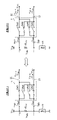
- the switches SW1 to SW4 in FIG. 2 are configured by the transistors TR1 to TR4 in FIG. 5, respectively.
- the switch control circuit 12 of FIG. 2 includes gate signal generation circuits 110 to 140 in addition to the clock output circuit 30 .
- Clock signal CLK1 output from clock output circuit 30 is applied to clock line LN1
- clock signal CLK2 output from clock output circuit 30 is applied to clock line LN2. It may be understood that the clock lines LN1 and LN2 are also included in the components of the switch control circuit 12.
- the gate signal generation circuits 110-140 generate gate signals for the transistors TR1-TR4, respectively.
- Gate signal generation circuits 110 to 140 have a common configuration.
- the gate signal generation circuit 110 includes a transistor TRa, capacitors 111 and 112 and a resistor 113 .
- the gate signal generation circuit 120 has a transistor TRb, capacitors 121 and 122 and a resistor 123 .
- the gate signal generation circuit 130 has a transistor TRc, capacitors 131 and 132 and a resistor 133 .
- the gate signal generation circuit 140 has a transistor TRd, capacitors 141 and 142 and a resistor 143 .
- the transistors TR1 to TR4 can be considered to function as main transistors, and in this case, the transistors TRa to TRd can be considered to function as sub-transistors.
- the transistors TR1-TR4 and TRa-TRd are P-channel MOSFETs. Assume that the absolute value of the gate threshold voltage Vth (eg, 0.6 V) of each of the transistors TR1-TR4 and TRa-TRd is smaller than the internal power supply voltage Vreg (eg, 4 V). Therefore, for example, when the gate potential of the transistor TR1 is lower than the source potential of the transistor TR1 by the voltage Vreg, the transistor TR1 is on. The same applies to transistors TR2-TR4 and TRa-TRd.
- the source of the transistor TR1 is connected to the terminal TM1, and the drain of the transistor TR1 is connected to the terminal 21.
- the source of transistor TRa is connected to terminal TM1, and the drain of transistor TRa is connected to node ND1.
- Node ND 1 is connected to the gate of transistor TR 1 and to the first end of capacitor 111 .
- a second end of capacitor 111 is connected to clock line LN1.
- the gate of transistor TRa is connected to node NDa.
- a first end of capacitor 112 is connected to node NDa and a second end of capacitor 112 is connected to clock line LN2.
- the node NDa is connected to the terminal TM1 through the resistor 113.
- the source of the transistor TR2 is connected to the terminal TM2, and the drain of the transistor TR2 is connected to the terminal 22.
- the source of transistor TRb is connected to terminal TM2, and the drain of transistor TRb is connected to node ND2.
- the node ND2 is connected to the gate of the transistor TR2 and to the first end of the capacitor 121 .
- a second end of capacitor 121 is connected to clock line LN1.
- the gate of transistor TRb is connected to node NDb.
- a first end of capacitor 122 is connected to node NDb, and a second end of capacitor 122 is connected to clock line LN2.
- the node NDb is connected through the resistor 123 to the terminal TM2.
- the source of the transistor TR3 is connected to the terminal TM1, and the drain of the transistor TR3 is connected to the terminal 22.
- the source of transistor TRc is connected to terminal TM1, and the drain of transistor TRc is connected to node ND3.
- Node ND3 is connected to the gate of transistor TR3 and to the first end of capacitor 131 .
- a second end of capacitor 131 is connected to clock line LN2.
- the gate of transistor TRc is connected to node NDc.
- a first end of capacitor 132 is connected to node NDc, and a second end of capacitor 132 is connected to clock line LN1.
- the node NDc is connected to the terminal TM1 through the resistor 133.
- the source of the transistor TR4 is connected to the terminal TM2, and the drain of the transistor TR4 is connected to the terminal 21.
- the source of transistor TRd is connected to terminal TM2, and the drain of transistor TRd is connected to node ND4.
- Node ND4 is connected to the gate of transistor TR4 and to the first end of capacitor 141 .
- a second end of capacitor 141 is connected to clock line LN2.
- the gate of transistor TRd is connected to node NDd.
- a first end of capacitor 142 is connected to node NDd, and a second end of capacitor 142 is connected to clock line LN1.
- the node NDd is connected through the resistor 143 to the terminal TM2.
- the change in level of clock signal CLK2 at time t 1 is transmitted through capacitor 112 to node NDa. Then, at time t1, the gate potential of the transistor TRa becomes lower than the source potential of the transistor TRa by the voltage Vreg, and as a result, the transistor TRa is turned on.
- the turn - on of transistor TRa at time t1 immediately causes the voltage at node ND1 to rise substantially to voltage V INM , and this rise causes the absolute value of the gate-source voltage of transistor TR1 to rise to the absolute value of gate threshold voltage Vth. , the transistor TR1 is turned off. Further, after time t 1 , charging current flows from terminal TM 1 to capacitor 112 through resistor 113 to increase the potential of node NDa, and at time t 2 the absolute value of the gate-source voltage of transistor TRa reaches the gate When the absolute value of the threshold voltage Vth becomes smaller than the absolute value, the transistor TRa is turned off.
- the time difference between times t 1 and t 2 shall be less than half of one period of clock signal CLK1 or CLK2 (the capacitance value of capacitor 112 and the resistance value of resistor 113 are set accordingly). ).
- Time t 3 is the time when half of one cycle of the clock signal CLK1 or CLK2 has elapsed from time t 1 .
- the voltage of node ND1 substantially matches voltage VINM .
- a down edge occurs in clock signal CLK1 and an up edge occurs in clock signal CLK2.
- the change in level of clock signal CLK1 at time t3 is transmitted through capacitor 111 to node ND1.
- the gate potential of the transistor TR1 becomes lower than the source potential of the transistor TR1 by the voltage Vreg, and as a result, the transistor TR1 is turned on.
- the circuit operation described above at time t1 is performed each time a falling edge occurs in clock signal CLK2, and the circuit operation described above at time t3 is performed each time a falling edge occurs in clock signal CLK1.
- the level change of the clock signal CLK2 is transmitted to the gates of the transistors TRa and TRb through the capacitors 112 and 122, thereby turning on the transistors TRa and TRb.
- This turns off transistors TR1 and TR2.
- the level change of the clock signal CLK1 reaches the gates of the transistors TR1 and TR2 through the capacitors 111 and 121 at the timing ( t3) of the down edge of the clock signal CLK1. , which turns on transistors TR1 and TR2.
- the change in level of clock signal CLK1 at time t3 is transmitted through capacitor 132 to node NDc . Then, at time t3 , the gate potential of the transistor TRc becomes lower than the source potential of the transistor TRc by the voltage Vreg, and as a result, the transistor TRc is turned on.
- the turn- on of transistor TRc at time t3 immediately causes the voltage at node ND3 to rise substantially to voltage V INM , and this rise causes the absolute value of the gate-source voltage of transistor TR3 to rise to the absolute value of gate threshold voltage Vth. , the transistor TR3 is turned off. After time t 3 , charging current flows from terminal TM 1 to capacitor 132 through resistor 133, and the potential of node NDc rises. At time t 4 , the absolute value of the gate-source voltage of transistor TRc reaches the gate When the absolute value of the threshold voltage Vth becomes smaller than the absolute value, the transistor TRc is turned off. It is assumed that the time difference between times t3 and t4 is less than half of one period of clock signal CLK1 or CLK2 (the capacitance value of capacitor 132 and the resistance value of resistor 133 are set accordingly). ).
- Time t 5 is the time when half of one cycle of clock signal CLK1 or CLK2 has elapsed from time t 3 .
- the voltage of node ND3 just before time t5 substantially matches voltage V INM .
- a down edge occurs in clock signal CLK2 and an up edge occurs in clock signal CLK1.
- the change in level of clock signal CLK2 at time t5 is transmitted through capacitor 131 to node ND3.
- the gate potential of the transistor TR3 becomes lower than the source potential of the transistor TR3 by the voltage Vreg, and as a result, the transistor TR3 is turned on.
- the circuit operation described above at time t3 is performed each time a falling edge occurs in clock signal CLK1, and the circuit operation described above at time t5 is performed each time a falling edge occurs in clock signal CLK2.
- the level change of the clock signal CLK1 is transmitted to the gates of the transistors TRc and TRd through the capacitors 132 and 142, thereby turning on the transistors TRc and TRd.
- This turns off transistors TR3 and TR4.
- the level change of the clock signal CLK2 is transmitted through the capacitors 131 and 141 to the gates of the transistors TR3 and TR4. , which turns on transistors TR3 and TR4.
- FIG. 8 collectively shows the waveforms of the signals and voltages of each part in FIG. 5 and the state transition of each transistor.
- a configuration (hereinafter referred to as a virtual configuration) in which a gate signal of internal power supply voltage Vreg or 0 V is supplied to each transistor constituting the switches SW1 to SW4 is adopted, then these transistors A voltage of 36V or 40V is applied between the gate and source. That is, in the virtual configuration, each transistor forming the switches SW1 to SW4 is required to have a high withstand voltage. Achieving a high withstand voltage results in an increase in the size of the transistor and an increase in the cost of the current sensor 10 .
- the withstand voltage of the semiconductor substrate connected to the terminals TM1, TM2, 21 and 22 is set to be equal to or higher than the common mode voltage VCM . Since the capacitors 23 and 24 are provided between the terminals 21 and 22 and the circuit 13, the breakdown voltage of each component in the circuit 13 does not depend on the common-mode voltage V CM and is slightly higher than the internal power supply voltage Vreg. Enough.
- the voltage Vreg is the voltage generated from the power supply voltage VDD, but the voltage Vreg may be the power supply voltage VDD supplied to the terminal TM4 from the outside of the current sensor 10 itself.
- the internal power supply circuit 14 can be omitted from the current sensor 10 .
- the sense resistor R SNS may be built in the current sensor 10 .
- the sense resistor R SNS may be provided on the lower potential side than the load LD.
- the current sensor 10 may be installed in a vehicle such as an automobile, and the current sensor 10 may be applied to any load LD in the vehicle.
- the application of the current sensor 10 is not limited to vehicle-mounted applications, and is arbitrary.
- FET field effect transistor
- a current sensor (10; see FIG. 1) includes first and second input terminals (TM1, TM2) configured to be connectable to both ends of a sense resistor (R SNS ), and the first and a second input terminal, and configured to generate a square wave signal having an amplitude proportional to the voltage across the sense resistor; and the sense resistor based on the square wave signal. and a current detection signal output circuit (13) capable of outputting a current detection signal (S OUT ) corresponding to the current flowing through (first configuration).
- the element that receives the voltages of the first and second input terminals must have a withstand voltage higher than the voltage applied to each input terminal.
- An increase in the required withstand voltage results in an increase in device size and cost. If a method of generating a square wave signal having an amplitude proportional to the voltage across the sense resistor and outputting a current detection signal based on the square wave signal as in the first configuration is used, the first and second input terminals It is possible to reduce the required breakdown voltage of the element that receives the voltage.
- the square wave generating circuit has first and second output terminals (21, 22) and a current between the first input terminal and the first output terminal.
- a first switch (SW1) provided in the second switch (SW2) provided between the second input terminal and the second output terminal; the first input terminal and the second output terminal; and a fourth switch (SW4) provided between the second input terminal and the first output terminal.
- the switch control circuit turns on the first switch and the second switch and turns off the third switch and the fourth switch.
- a first state (ST1) in which the control is performed and a second state (ST2) in which the first switch and the second switch are in an OFF state and the third switch and the fourth switch are in an ON state are alternately controlled.
- a configuration (third configuration) configured to generate the square wave signal between the first output terminal and the second output terminal by switching to .
- the first to fourth switches are first to fourth main transistors (TR1 to TR4) composed of field effect transistors, respectively, and the switch control circuit are provided between the first sub-transistor (TRa) provided between the first input terminal and the gate of the first main transistor, and the second input terminal and the gate of the second main transistor; a second sub-transistor (TRb), a third sub-transistor (TRc) provided between the first input terminal and the gate of the third main transistor, the second input terminal and the fourth main transistor A fourth sub-transistor (TRd) provided between the gate of , a first clock signal (CLK1) which is a rectangular wave signal, and a second clock signal (CLK2 ), wherein said switch control circuit controls the gate voltage of each main transistor through each sub-transistor using said first and second clock signals. Therefore, a configuration (fourth configuration) in which each main transistor can be controlled to be on or off may be employed.
- the switch control circuit includes a first gate signal generation circuit (110) including the first sub-transistor and a second gate signal generating circuit (110) including the second sub-transistor.
- the first capacitor (121) is provided between the gate of the second main transistor and the first clock line
- the second capacitor (122 ) is provided between the gate of the second sub-transistor and the second clock line
- the resistor (123) is provided between the gate of the second sub-transistor and the second input terminal.
- the first capacitor (131) is provided between the gate of the third main transistor and the second clock line
- the second capacitor (132) is provided between the third gate signal generation circuit
- the resistor (133) is provided between the gate of the third sub-transistor and the first clock line
- the resistor (133) is provided between the gate of the third sub-transistor and the first input terminal.
- the first capacitor (141) is provided between the gate of the fourth main transistor and the second clock line
- the second capacitor (142) is provided between the fourth sub-transistor. and the first clock line
- the resistor (143) is provided between the gate of the fourth sub-transistor and the second input terminal (fifth configuration)
- the voltage applied between the electrodes of each transistor can be made equal to or less than the potential difference between the first and second levels regardless of the voltage applied to the first or second input terminal.
- each transistor does not need to have a withstand voltage corresponding to the voltage applied to the first or second input terminal, and the size of each transistor can be reduced.
- each signal level of the first and second clock signals varies between different first and second levels, whereby the signal level of the first clock signal changes to the a first timing (t 1 , t 5 ) at which the signal level of the second clock signal is switched from the second level to the first level as the level 1 is switched to the second level, and the signal level of the first clock signal; is switched from the second level to the first level and the signal level of the second clock signal is switched from the first level to the second level at a second timing (t 3 ).
- the level change of the second clock signal is transmitted to the gates of the first and second sub-transistors through the second capacitors in the first and second gate signal generation circuits.
- the third and fourth sub-transistors are turned on by being transmitted to the gates of the third and fourth sub-transistors through the second capacitors in the signal generation circuit, thereby turning on the third and fourth main transistors.
- the level change of the second clock signal A configuration in which the third and fourth main transistors are turned on by being transmitted to the gates of the third and fourth main transistors through the first capacitors in the third and fourth gate signal generation circuits (sixth configuration) may be
Landscapes
- Physics & Mathematics (AREA)
- General Physics & Mathematics (AREA)
- Engineering & Computer Science (AREA)
- Computer Hardware Design (AREA)
- Power Engineering (AREA)
- Computing Systems (AREA)
- General Engineering & Computer Science (AREA)
- Mathematical Physics (AREA)
- Electronic Switches (AREA)
Priority Applications (2)
| Application Number | Priority Date | Filing Date | Title |
|---|---|---|---|
| JP2023533442A JP7827721B2 (ja) | 2021-07-05 | 2022-04-08 | 電流センサ |
| US18/397,828 US20240125823A1 (en) | 2021-07-05 | 2023-12-27 | Current sensor |
Applications Claiming Priority (2)
| Application Number | Priority Date | Filing Date | Title |
|---|---|---|---|
| JP2021111297 | 2021-07-05 | ||
| JP2021-111297 | 2021-07-05 |
Related Child Applications (1)
| Application Number | Title | Priority Date | Filing Date |
|---|---|---|---|
| US18/397,828 Continuation US20240125823A1 (en) | 2021-07-05 | 2023-12-27 | Current sensor |
Publications (1)
| Publication Number | Publication Date |
|---|---|
| WO2023281891A1 true WO2023281891A1 (ja) | 2023-01-12 |
Family
ID=84800203
Family Applications (1)
| Application Number | Title | Priority Date | Filing Date |
|---|---|---|---|
| PCT/JP2022/017357 Ceased WO2023281891A1 (ja) | 2021-07-05 | 2022-04-08 | 電流センサ |
Country Status (3)
| Country | Link |
|---|---|
| US (1) | US20240125823A1 (https=) |
| JP (1) | JP7827721B2 (https=) |
| WO (1) | WO2023281891A1 (https=) |
Citations (6)
| Publication number | Priority date | Publication date | Assignee | Title |
|---|---|---|---|---|
| JP2000231940A (ja) * | 1999-02-10 | 2000-08-22 | Marunitto:Kk | バッテリーメーター |
| JP2002311065A (ja) * | 2001-04-17 | 2002-10-23 | Seiko Instruments Inc | 充放電電流検出回路 |
| JP2004309386A (ja) * | 2003-04-09 | 2004-11-04 | Toyota Motor Corp | 電流検出装置 |
| WO2009122520A1 (ja) * | 2008-03-31 | 2009-10-08 | 三菱電機株式会社 | モータ駆動制御装置 |
| CN206411180U (zh) * | 2016-10-20 | 2017-08-15 | 森达因公司 | 相对于第一测量点和第二测量点来测量电流的设备 |
| WO2021085475A1 (ja) * | 2019-11-01 | 2021-05-06 | 国立研究開発法人科学技術振興機構 | 電流センサおよび電力変換回路 |
Family Cites Families (2)
| Publication number | Priority date | Publication date | Assignee | Title |
|---|---|---|---|---|
| US7834613B2 (en) * | 2007-10-30 | 2010-11-16 | Power-One, Inc. | Isolated current to voltage, voltage to voltage converter |
| EP3907511B1 (en) * | 2020-05-08 | 2024-09-04 | Hamilton Sundstrand Corporation | Radiation hardened magnetic current sensor |
-
2022
- 2022-04-08 JP JP2023533442A patent/JP7827721B2/ja active Active
- 2022-04-08 WO PCT/JP2022/017357 patent/WO2023281891A1/ja not_active Ceased
-
2023
- 2023-12-27 US US18/397,828 patent/US20240125823A1/en active Pending
Patent Citations (6)
| Publication number | Priority date | Publication date | Assignee | Title |
|---|---|---|---|---|
| JP2000231940A (ja) * | 1999-02-10 | 2000-08-22 | Marunitto:Kk | バッテリーメーター |
| JP2002311065A (ja) * | 2001-04-17 | 2002-10-23 | Seiko Instruments Inc | 充放電電流検出回路 |
| JP2004309386A (ja) * | 2003-04-09 | 2004-11-04 | Toyota Motor Corp | 電流検出装置 |
| WO2009122520A1 (ja) * | 2008-03-31 | 2009-10-08 | 三菱電機株式会社 | モータ駆動制御装置 |
| CN206411180U (zh) * | 2016-10-20 | 2017-08-15 | 森达因公司 | 相对于第一测量点和第二测量点来测量电流的设备 |
| WO2021085475A1 (ja) * | 2019-11-01 | 2021-05-06 | 国立研究開発法人科学技術振興機構 | 電流センサおよび電力変換回路 |
Also Published As
| Publication number | Publication date |
|---|---|
| JP7827721B2 (ja) | 2026-03-10 |
| US20240125823A1 (en) | 2024-04-18 |
| JPWO2023281891A1 (https=) | 2023-01-12 |
Similar Documents
| Publication | Publication Date | Title |
|---|---|---|
| TWI261967B (en) | Rush current limiting circuit for a PFM control charge pump | |
| US6664822B2 (en) | Driving device having dummy circuit | |
| US6323697B1 (en) | Low distortion sample and hold circuit | |
| US6459322B1 (en) | Level adjustment circuit and data output circuit thereof | |
| CN103248335B (zh) | 具有隔离阻障件的逻辑信号传输电路 | |
| JP4926275B2 (ja) | トランジスタスナップバック保護を組み込むレベルシフタ回路 | |
| US10715132B2 (en) | Gate driver circuit of power transistor, and motor driver circuit | |
| JP7282599B2 (ja) | ハイサイドトランジスタの駆動回路、スイッチング回路、dc/dcコンバータのコントローラ | |
| US7443200B2 (en) | Capacitor-coupled level shifter with duty-cycle independence and supply referenced bias configuration | |
| CN108377090B (zh) | 开关电容电路及其操作方法、电流感测电路和集成电路 | |
| US7239185B2 (en) | Driver circuit connected to pulse shaping circuitry | |
| JP2022144130A (ja) | ハイサイドトランジスタの駆動回路、スイッチング回路、dc/dcコンバータのコントローラ | |
| US20230353134A1 (en) | Voltage comparison circuit | |
| CN107276408A (zh) | 电路装置、开关调节器以及电子设备 | |
| US8253441B1 (en) | Circuits and methods for level shifting a signal | |
| WO2018020783A1 (ja) | リンギング抑制回路 | |
| US20090289685A1 (en) | Bias voltage generation for capacitor-coupled level shifter with supply voltage tracking and compensation for input duty-cycle variation | |
| CN100414837C (zh) | 用来生成提供给电导体的电路输出信号的电子驱动器电路 | |
| JP7827721B2 (ja) | 電流センサ | |
| US20050110553A1 (en) | Level shifter | |
| JP4371645B2 (ja) | 半導体装置 | |
| US8174294B1 (en) | Configurable buffer circuits and methods | |
| US20030184395A1 (en) | CR oscillation circuit | |
| US8593179B2 (en) | Delay circuit and inverter for semiconductor integrated device | |
| CN101399525A (zh) | 电压电平箝制电路与比较器模块 |
Legal Events
| Date | Code | Title | Description |
|---|---|---|---|
| 121 | Ep: the epo has been informed by wipo that ep was designated in this application |
Ref document number: 22837312 Country of ref document: EP Kind code of ref document: A1 |
|
| WWE | Wipo information: entry into national phase |
Ref document number: 2023533442 Country of ref document: JP |
|
| NENP | Non-entry into the national phase |
Ref country code: DE |
|
| 122 | Ep: pct application non-entry in european phase |
Ref document number: 22837312 Country of ref document: EP Kind code of ref document: A1 |