WO2023244875A1 - Photonic integrated circuit multi-wavelength phase modulator networks - Google Patents
Photonic integrated circuit multi-wavelength phase modulator networks Download PDFInfo
- Publication number
- WO2023244875A1 WO2023244875A1 PCT/US2023/063127 US2023063127W WO2023244875A1 WO 2023244875 A1 WO2023244875 A1 WO 2023244875A1 US 2023063127 W US2023063127 W US 2023063127W WO 2023244875 A1 WO2023244875 A1 WO 2023244875A1
- Authority
- WO
- WIPO (PCT)
- Prior art keywords
- optical signals
- phase modulator
- optical
- unit cell
- spectrally
- Prior art date
- Legal status (The legal status is an assumption and is not a legal conclusion. Google has not performed a legal analysis and makes no representation as to the accuracy of the status listed.)
- Ceased
Links
Classifications
-
- G—PHYSICS
- G02—OPTICS
- G02B—OPTICAL ELEMENTS, SYSTEMS OR APPARATUS
- G02B6/00—Light guides; Structural details of arrangements comprising light guides and other optical elements, e.g. couplings
- G02B6/10—Light guides; Structural details of arrangements comprising light guides and other optical elements, e.g. couplings of the optical waveguide type
- G02B6/12—Light guides; Structural details of arrangements comprising light guides and other optical elements, e.g. couplings of the optical waveguide type of the integrated circuit kind
- G02B6/12004—Combinations of two or more optical elements
-
- G—PHYSICS
- G02—OPTICS
- G02F—OPTICAL DEVICES OR ARRANGEMENTS FOR THE CONTROL OF LIGHT BY MODIFICATION OF THE OPTICAL PROPERTIES OF THE MEDIA OF THE ELEMENTS INVOLVED THEREIN; NON-LINEAR OPTICS; FREQUENCY-CHANGING OF LIGHT; OPTICAL LOGIC ELEMENTS; OPTICAL ANALOGUE/DIGITAL CONVERTERS
- G02F1/00—Devices or arrangements for the control of the intensity, colour, phase, polarisation or direction of light arriving from an independent light source, e.g. switching, gating or modulating; Non-linear optics
- G02F1/29—Devices or arrangements for the control of the intensity, colour, phase, polarisation or direction of light arriving from an independent light source, e.g. switching, gating or modulating; Non-linear optics for the control of the position or the direction of light beams, i.e. deflection
- G02F1/292—Devices or arrangements for the control of the intensity, colour, phase, polarisation or direction of light arriving from an independent light source, e.g. switching, gating or modulating; Non-linear optics for the control of the position or the direction of light beams, i.e. deflection by controlled diffraction or phased-array beam steering
-
- G—PHYSICS
- G02—OPTICS
- G02B—OPTICAL ELEMENTS, SYSTEMS OR APPARATUS
- G02B27/00—Optical systems or apparatus not provided for by any of the groups G02B1/00 - G02B26/00, G02B30/00
- G02B27/0087—Phased arrays
-
- G—PHYSICS
- G02—OPTICS
- G02B—OPTICAL ELEMENTS, SYSTEMS OR APPARATUS
- G02B6/00—Light guides; Structural details of arrangements comprising light guides and other optical elements, e.g. couplings
- G02B6/10—Light guides; Structural details of arrangements comprising light guides and other optical elements, e.g. couplings of the optical waveguide type
- G02B6/12—Light guides; Structural details of arrangements comprising light guides and other optical elements, e.g. couplings of the optical waveguide type of the integrated circuit kind
- G02B6/12007—Light guides; Structural details of arrangements comprising light guides and other optical elements, e.g. couplings of the optical waveguide type of the integrated circuit kind forming wavelength selective elements, e.g. multiplexer, demultiplexer
- G02B6/12009—Light guides; Structural details of arrangements comprising light guides and other optical elements, e.g. couplings of the optical waveguide type of the integrated circuit kind forming wavelength selective elements, e.g. multiplexer, demultiplexer comprising arrayed waveguide grating [AWG] devices, i.e. with a phased array of waveguides
- G02B6/12014—Light guides; Structural details of arrangements comprising light guides and other optical elements, e.g. couplings of the optical waveguide type of the integrated circuit kind forming wavelength selective elements, e.g. multiplexer, demultiplexer comprising arrayed waveguide grating [AWG] devices, i.e. with a phased array of waveguides characterised by the wavefront splitting or combining section, e.g. grooves or optical elements in a slab waveguide
-
- G—PHYSICS
- G02—OPTICS
- G02B—OPTICAL ELEMENTS, SYSTEMS OR APPARATUS
- G02B6/00—Light guides; Structural details of arrangements comprising light guides and other optical elements, e.g. couplings
- G02B6/10—Light guides; Structural details of arrangements comprising light guides and other optical elements, e.g. couplings of the optical waveguide type
- G02B6/12—Light guides; Structural details of arrangements comprising light guides and other optical elements, e.g. couplings of the optical waveguide type of the integrated circuit kind
- G02B2006/12035—Materials
-
- G—PHYSICS
- G02—OPTICS
- G02F—OPTICAL DEVICES OR ARRANGEMENTS FOR THE CONTROL OF LIGHT BY MODIFICATION OF THE OPTICAL PROPERTIES OF THE MEDIA OF THE ELEMENTS INVOLVED THEREIN; NON-LINEAR OPTICS; FREQUENCY-CHANGING OF LIGHT; OPTICAL LOGIC ELEMENTS; OPTICAL ANALOGUE/DIGITAL CONVERTERS
- G02F1/00—Devices or arrangements for the control of the intensity, colour, phase, polarisation or direction of light arriving from an independent light source, e.g. switching, gating or modulating; Non-linear optics
- G02F1/01—Devices or arrangements for the control of the intensity, colour, phase, polarisation or direction of light arriving from an independent light source, e.g. switching, gating or modulating; Non-linear optics for the control of the intensity, phase, polarisation or colour
- G02F1/0147—Devices or arrangements for the control of the intensity, colour, phase, polarisation or direction of light arriving from an independent light source, e.g. switching, gating or modulating; Non-linear optics for the control of the intensity, phase, polarisation or colour based on thermo-optic effects
Definitions
- This disclosure relates generally to optical systems. More specifically, this disclosure relates to photonic integrated circuit multi -wavelength phase modulator networks.
- Next-generation optical phased arrays are being designed for use in free- space optical systems, which refer to systems where optical signals are transmitted and received through free space rather than through optical fibers. These optical phased arrays are often implemented using photonic integrated circuits (PICs).
- PICs photonic integrated circuits
- a photonic integrated circuit refers to a device that integrates multiple photonic or light-based functions into the device.
- a photonic integrated circuit may include an array of nano-antennas, which represent extremely small antennas that can be used for transmitting or receiving optical signals.
- This disclosure relates to photonic integrated circuit multi -wavelength phase modulator networks.
- an apparatus in a first embodiment, includes a photonic integrated circuit having an optical phased array, where the optical phased array includes multiple unit cells.
- Each unit cell includes at least one antenna element configured to transmit or receive multiple optical signals having spectrally-distinct wavelengths or wavelength ranges.
- Each unit cell also includes at least one signal pathway configured to transport the optical signals to or from the at least one antenna element.
- Each unit cell further includes a phase modulator configured to modify phases of the optical signals being transported through the at least one signal pathway.
- Each unit cell is configured to provide correlated phase shifts to the optical signals having the spectrally-distinct wavelengths or wavelength ranges.
- a method in a second embodiment, includes transmitting or receiving optical signals having spectrally-distinct wavelengths or wavelength ranges at a photonic integrated circuit having an optical phased array.
- the optical phased array includes multiple unit cells.
- the unit cells include (i) antenna elements configured to transmit or receive the optical signals, (ii) signal pathways configured to transport the optical signals to or from the antenna elements, and (iii) phase modulators configured to modify phases of the optical signals being transported through the signal pathways.
- the method also includes providing correlated phase shifts to the optical signals having the spectrally-distinct wavelengths or wavelength ranges using the unit cells.
- an apparatus in a third embodiment, includes a photonic integrated circuit having an optical phased array, where the optical phased array includes multiple unit cells.
- Each unit cell includes means for transmitting or receiving multiple optical signals having spectrally-distinct wavelengths or wavelength ranges, means for transporting the optical signals to or from the at least one antenna element, and means for modifying phases of the optical signals being transported through the at least one signal pathway.
- Each unit cell is configured to provide correlated phase shifts to the optical signals having the spectrally-distinct wavelengths or wavelength ranges.
- FIGURE 1 illustrates an example system supporting optical communications using photonic integrated circuit multi -wavelength phase modulator networks according to this disclosure
- FIGURE 2 illustrates a specific example system supporting optical communications using photonic integrated circuit multi -wavelength phase modulator networks according to this disclosure
- FIGURES 3 through 6 illustrate an example optical device supporting photonic integrated circuit multi -wavelength phase modulator networks according to this disclosure
- FIGURES 7 through 11 illustrate example multi -wavelength phase modulator networks according to this disclosure.
- FIGURES 12 and 13 illustrate example phase modulators for use in photonic integrated circuit multi -wavelength phase modulator networks according to this disclosure.
- FIGURES 1 through 13, described below, and the various embodiments used to describe the principles of the present disclosure are by way of illustration only and should not be construed in any way to limit the scope of this disclosure. Those skilled in the art will understand that the principles of the present disclosure may be implemented in any type of suitably arranged device or system.
- next-generation optical phased arrays OP As
- PICs photonic integrated circuits
- a photonic integrated circuit refers to a device that integrates multiple photonic or light-based functions into the device.
- a photonic integrated circuit may include an array of nano-antennas, which represent extremely small antennas that can be used for transmitting or receiving optical signals.
- Optical phased arrays are often used to transmit or receive optical signals at different wavelengths or within different wavelength ranges.
- transmitted and received optical signals that are used for data communications or other purposes may be at different wavelengths or within different wavelength ranges in order to allow for simultaneous transmission and reception of the optical signals.
- beacon signals are also used and may be at a different wavelength or within a different wavelength range than the optical signals used for data communications or other purposes.
- Phase modulators in the optical phased arrays can be used in order to control the phases of incoming or outgoing optical signals. However, these phase modulators may have inadequate bandwidth to cover all of the wavelengths or wavelength ranges used by the optical phased arrays.
- phase modulators While it may be possible to duplicate the phase modulators and use different phase modulators depending on the incoming or outgoing optical transmissions being performed, this increases the size, weight, power, and cost (SWAP-C) of the optical devices. Moreover, phase modulators are often too large to achieve a unity fill factor and a 180° field of regard, which can result in increased optical losses, reduced data rates, or limited angles at which optical devices can effectively communicate. Duplicating the phase modulators to support different wavelengths or different wavelength ranges exacerbates these issues even more.
- phase modulator network includes an array of phase modulators, such as micro-ring resonators or other phase modulators, that operate in conjunction with multiple input/output (I/O) ports.
- phase modulators can be designed and controlled in order to adjust the phases of optical signals provided to or received from one or more of the I/O ports.
- the phase modulators can support the modification of the phases of the optical signals over a wide bandwidth, such as a bandwidth that includes transmit, receive, and beacon wavelengths or wavelength ranges.
- the phase modulators can support the use of multiple polarizations, as well.
- each phase modulator may be implemented using a micro-ring resonator, and signal pathways for optical signals of different wavelengths or different wavelength ranges may pass along different arc portions of each micro-ring resonator.
- Coupling waveguides and coupling gaps for the signal pathways and the micro-ring resonators can differ slightly, which makes the resonance peak of each micro-ring resonator identical or nearly identical for different wavelengths or wavelength ranges.
- optical devices can use the same phase modulators to modify different incoming or outgoing optical signals that are at different wavelengths or in different wavelength ranges. This can help to reduce or avoid the need to provide multiple phase modulators and associated controllers to support the use of the different wavelengths or different wavelength ranges, which can help to reduce the size, weight, power, and cost of the optical devices. Moreover, this can help to increase the fill factors and link efficiencies of the optical devices. In addition, this may allow for the optical devices to inherently correlate phase control for all wavelengths or wavelength ranges used by the optical devices, such as by enabling intrinsically-correlated phase control (with no relative phase errors/slips between wavelengths).
- FIGURE 1 illustrates an example system 100 supporting optical communications using photonic integrated circuit multi -wavelength phase modulator networks according to this disclosure.
- the system 100 includes two nodes 102 and 104 that communicate with one another optically.
- Each node 102 and 104 represents a ground-, air-, or space-based system that can transmit or receive data using optical communications.
- the nodes 102 and 104 can engage in bidirectional communication with one another. However, this is not necessarily required, and the nodes 102 and 104 may engage in unidirectional communication with one another (meaning one node 102 or 104 may only transmit and the other node 104 or 102 may only receive, at least with respect to each other).
- the node 102 in this example includes an optical transmitter 106, which generally operates to produce optical signals 108 used for communication or other purposes.
- the optical transmitter 106 may encode information onto the optical signals 108, such as by using suitable amplitude, phase, frequency, or other modulation(s) of light.
- the optical signals 108 can be transmitted through free space or other transmission medium to the node 104, where an optical receiver 110 receives and processes the optical signals 108.
- the optical receiver 110 can identify the amplitude, phase, frequency, or other modulation(s) of light in the optical signals 108 and use the identified modulation(s) to recover the information encoded onto the optical signals 108.
- any suitable type of modulation/demodulation scheme may be used here to encode and decode the optical signals 108 (assuming communication is one purpose of the optical signals 108). Since the nodes 102 and 104 are bidirectional in this example, the same process can be used in the opposite direction, meaning an optical transmitter 112 of the node 104 produces optical signals 114 that are transmitted towards the node 102 and received and processed by an optical receiver 116 of the node 102.
- the nodes 102 and 104 may use different wavelengths or wavelength ranges when interacting with each other.
- the node 102 may use one or more first wavelengths or wavelength ranges to transmit the optical signals 108 to the node 104
- the node 104 may use one or more second wavelengths or wavelength ranges to transmit the optical signals 108 to the node 102. Assuming the first and second wavelengths or wavelength ranges are adequately separated, this may allow each node 102 and 104 to simultaneously transmit and receive the optical signals 108 and 114.
- the node 102 may transmit multiple types of optical signals 108 to the node 104
- the node 104 may transmit multiple types of optical signals 114 to the node 102.
- each node 102 and 104 may transmit beacon signals to the other node and optionally to other nearby or visible nodes (where the beacon signals have a different wavelength or wavelength range than those used for data transmission and reception or other purposes).
- a beacon signal can be transmitted from a first node to allow a second node to identify the first node and determine an approximate position or angle of the first node relative to the second node. This may allow the nodes to identify one another and generally aim subsequent optical communications towards each another. Once identified (and possibly validated or otherwise approved), the nodes 102 and 104 may then exchange additional optical signals 108 and 114 in order to support data communications or other functions.
- optical transmitter 106 and the optical receiver 116 are shown here as separate components, they can be integrated into a single optical transceiver 118. This may allow, for example, the same PIC-based structure to be used for both transmission and reception purposes.
- optical transmitter 112 and the optical receiver 110 are shown here as separate components, they can be integrated into a single optical transceiver 120. This may allow, for instance, the same PIC-based structure to be used for both transmission and reception purposes.
- each of the optical transmitters 106 and 112, optical receivers 110 and 116, or optical transceivers 118 and 120 includes at least one photonic integrated circuit that implements at least one optical phased array.
- Each optical phased array may include a multi -wavelength phase modulator network, such as an array of micro-ring resonators or other phase modulators that can operate over multiple wavelengths or wavelength ranges.
- the multiple wavelengths or wavelength ranges can include the wavelengths or wavelength ranges used by optical signals for data communications or other purposes and by beacon optical signals.
- the optical transmitters, receivers, and transceivers described in this disclosure may find use in a large number of applications.
- optical transmitters, receivers, or transceivers may be used in data centers or telecommunication systems to transport information rapidly between locations, including the transport of large amounts of information over very large distances.
- Optical transmitters, receivers, or transceivers may be used in consumer or commercial electronic devices, biomedical devices, or advanced computing devices to support optical-based communications with those devices.
- Optical transmitters, receivers, or transceivers may be used in airplanes, drones, satellites, autonomous vehicles, rockets, missiles, or other commercial or defense-related systems.
- Optical transmitters, receivers, or transceivers may be used in non- communication-related optical applications, such as laser detection and ranging (LADAR) applications or other applications that can use polarimetric processing with PIC -based optical phased arrays.
- LADAR laser detection and ranging
- this disclosure is not limited to any particular application of the optical transmitters, receivers, and transceivers.
- FIGURE 1 illustrates one example of a system 100 supporting optical communications using photonic integrated circuit multi -wavelength phase modulator networks
- the system 100 may include any suitable number of nodes that engage in any suitable unidirectional, bidirectional, or other communications or other interactions with each other.
- each node of the system 100 may include any suitable number of optical transmitters, receivers, or transceivers that communicate or otherwise use any number of optical signals.
- the system 100 is shown in simplified form here and may include any number of additional components in any suitable configuration as needed or desired.
- FIGURE 2 illustrates a specific example system 200 supporting optical communications using photonic integrated circuit multi-wavelength phase modulator networks according to this disclosure.
- the system 200 includes two satellites 202 and 204 that can engage in unidirectional or bidirectional communication with one another.
- the satellite 202 is shown as transmitting beacon optical signals 206 towards the satellite 204
- the satellite 204 is shown as transmitting beacon optical signals 208 towards the satellite 202.
- the beacon optical signals 206 and 208 allow each of the satellites 202 and 204 to identify the other satellite and determine the position or angle of the other satellite.
- the satellite 202 is also shown as transmitting optical signals 210 towards the satellite 204
- the satellite 204 is also shown as transmitting optical signals 212 towards the satellite 202.
- the optical signals 210 and 212 may be used for other purposes, such as data communications involving the satellites 202 and 204. As can be seen here, each satellite 202 or 204 can transmit the optical signals 210 or 212 over a narrower angle, which may be possible once each satellite 202 or 204 identifies the position or angle of the other satellite using the associated beacon optical signals 206 or 208.
- Each satellite 202 and 204 includes one or more PIC-based optical transmitters, receivers, or transceivers 214 that enable the satellites 202 and 204 to engage in free-space optical communications.
- the satellites 202 and 204 may represent specific implementations of the nodes 102 and 104 described above
- the PIC-based transmitters, receivers, or transceivers 214 may represent specific implementations of the optical transmitters 106 and 112, optical receivers 110 and 116, or optical transceivers 118 and 120 described above.
- Each PIC-based transmitter, receiver, or transceiver 214 may implement at least one optical phased array.
- Each optical phased array may include a multi -wavelength phase modulator network, such as an array of micro-ring resonators or other phase modulators that can operate over multiple wavelengths or wavelength ranges.
- the multiple wavelengths or wavelength ranges can include the wavelengths or wavelength ranges used by optical signals 210 and 212 for data communications or other purposes and by beacon optical signals 206 and 208.
- the satellites 202 and 204 shown here may represent any suitable satellites that engage in optical communications or other functions.
- the satellites 202 and 204 may represent satellites in a proliferated low Earth orbit constellation, although other types of satellites in other orbits or constellations may be used.
- FIGURE 2 illustrates one specific example of a system 200 supporting optical communications using photonic integrated circuit multi -wavelength phase modulator networks
- the system 200 may include any suitable number of satellites that engage in any suitable unidirectional, bidirectional, or other communications or other interactions with each other.
- each satellite of the system 200 may include any suitable number of optical transmitters, receivers, or transceivers that communicate or otherwise use any number of optical signals.
- the example system 200 shown here uses satellites, other systems may use other types of nodes that engage in optical communications.
- nodes using PIC -based optical transmitters, receivers, or transceivers may be used in a ground-based free- space optical communication system to support mid- and last-mile communications.
- FIGURES 3 through 6 illustrate an example optical device 300 supporting photonic integrated circuit multi -wavelength phase modulator networks according to this disclosure.
- the optical device 300 here may represent a specific implementation of at least a portion of an optical node 102 or 104 or satellite 202 or 204 described above.
- the optical device 300 includes a package 302, which surrounds and protects electronic and optical components of an optical transmitter, optical receiver, or optical transceiver.
- the package 302 may encase and form a hermetic seal around the electronic and optical components.
- the package 302 may be formed from any suitable material(s), such as one or more metals, and in any suitable manner.
- the package 302 is formed using a nickel-cobalt or nickel-iron alloy (such as KOVAR) or other material that has a coefficient of thermal expansion closely matched to that of borosilicate or other glass.
- the package 302 may also have any suitable size, shape, and dimensions.
- the package 302 may be formed in multiple parts that can be bonded, sealed, or otherwise coupled together to enclose the electronic and optical components.
- the package 302 may be formed using a larger lower portion and an upper cover such that the electronic and optical components can be inserted into the lower portion and the upper cover can be connected to the lower portion.
- the package 302 may include flanges 304 that support mounting of the package 302 to a larger structure.
- the package 302 may have any other suitable form.
- the package 302 includes an optical window 306, which is substantially or completely transparent optically (at least with respect to the optical signals being transmitted from or received by the optical device 300).
- the optical window 306 may be formed from any suitable material(s), such as borosilicate glass or other glass, and in any suitable manner.
- the optical window 306 may also have any suitable size, shape, and dimensions. In some cases, the optical window 306 may also function as a bandpass or other optical filter that filters the wavelength(s) of the optical signals being transmitted from or received by the optical device 300.
- the package 302 may also include one or more electrical feedthroughs 308, which represent one or more electrical connections that can be used to transport one or more electrical signals between the interior and the exterior of the package 302.
- the one or more electrical signals may be used here for any suitable purposes, such as to control one or more operations of the optical device 300.
- the one or more electrical signals may be used for controlling the phases of antenna elements of a photonic integrated circuit in the optical device 300.
- the package 302 may include one or more fiber inputs/outputs 310, which can be used to provide one or more input signals to the optical device 300 and/or receive one or more output signals from the optical device 300.
- the one or more input signals may carry information to be transmitted from the optical device 300.
- the one or more output signals may carry information received at and recovered by the optical device 300.
- there are two fiber inputs/outputs 310 although the optical device 300 may include a single fiber input/output 310 or more than two fiber inputs/outputs 310. Note, however, that no fiber inputs/outputs 310 may be needed if all optical generation and processing occurs using components within the package 302, in which case the electrical feedthroughs 308 may be used to transport information to or from the optical device 300.
- a photonic integrated circuit 402 is positioned within the package 302, namely at a location where the photonic integrated circuit 402 can transmit and/or receive optical signals through the optical window 306.
- the photonic integrated circuit 402 may, for example, include a PIC -based optical phased array as described in more detail below.
- the photonic integrated circuit 402 can be used to support optical transmission and/or optical reception, depending on the design of the photonic integrated circuit 402.
- the photonic integrated circuit 402 may also support a number of additional optical functions as needed or desired.
- the photonic integrated circuit 402 may be formed from any suitable material(s), such as silicon, indium phosphide, or gallium arsenide, and in any suitable manner.
- the photonic integrated circuit 402 may also have any suitable size, shape, and dimensions. As a particular example, the photonic integrated circuit 402 may be square and have an edge length of about 40 mm, although any other suitable sizes and shapes may be used here.
- Fiber mounts 404 are used to couple to optical fibers 406 at locations where the optical fibers 406 can provide optical signals to and/or receive optical signals from the photonic integrated circuit 402.
- the optical fibers 406 may provide optical signals from a source laser to the photonic integrated circuit 402 for use during outgoing transmissions.
- the optical fibers 406 may also or alternatively provide optical signals received by the photonic integrated circuit 402 to a receiver for processing.
- Each fiber mount 404 includes any suitable structure configured to be coupled to an optical fiber 406.
- Each optical fiber 406 represents any suitable length of an optical medium configured to transport optical signals to or from a photonic integrated circuit 402.
- the optical device 300 may include, one, two, three, or more than four fiber mounts 404 and optical fibers 406. Also note that no fiber mounts 404 and optical fibers 406 may be needed if all optical generation and processing occurs using components of the photonic integrated circuit 402.
- An electronic control board 408 includes electronic components, such as one or more integrated circuit chips and other components, that control the operation of the photonic integrated circuit 402.
- the electronic control board 408 may include one or more components that calculate desired phases or phase corrections for optical signals to be generated by antenna elements of the photonic integrated circuit 402, which allows the electronic control board 408 to control functions such as beam forming or beam steering operations.
- the electronic control board 408 may include one or more components that calculate desired phases or phase corrections to be applied to optical signals received by antenna elements of the photonic integrated circuit 402, which allows the electronic control board 408 to control functions such as wavefront reconstruction operations.
- the electronic control board 408 includes any suitable components configured to perform one or more desired functions related to a photonic integrated circuit 402.
- Spacers 410 may be positioned on opposite sides of the photonic integrated circuit 402 and used to help separate the optical fibers 406 from the electronic control board 408.
- the spacers 410 may be formed from any suitable material(s), such as ceramic, and in any suitable manner.
- the photonic integrated circuit 402 includes a PIC-based optical phased array 502, where the optical phased array 502 includes a large number of unit cells 504.
- Each unit cell 504 is configured to transmit or receive one or more optical signals.
- each unit cell 504 includes a phase modulator configured to modulate the phases of optical signals flowing through one or more signal pathways of the unit cell 504.
- the optical phased array 502 can include any suitable number of unit cells 504, possibly up to and including a very large number of unit cells 504.
- the optical phased array 502 may include an array of unit cells 504 up to a size of 1024x 1024 (meaning over one million unit cells 504) or even larger.
- the optical phased array 502 may include multiple groups 506 of unit cells 504, where the unit cells 504 in each group 506 are fed an outgoing optical signal or are used to generate an incoming optical signal.
- the optical phased array 502 may include sixteen groups 506 of unit cells 504 arranged in a 4x4 pattern, although other numbers and arrangements of groups 506 of unit cells 504 may be used.
- the size of the optical phased array 502 is based, at least in part, on the number and size of the unit cells 504 and the number and arrangement of the groups 506.
- the optical phased array 502 may be scaled to various sizes as needed or desired.
- a feed network 508 is used to split outgoing optical signals for transmission by the optical phased array 502 or to combine incoming optical signals received by the optical phased array 502.
- the feed network 508 may include a collection of splitters/combiners that can divide optical signals flowing in one direction through the feed network 508 and combine optical signals flowing in the opposite direction through the feed network 508.
- the feed network 508 can be designed to feed optical signals to or receive optical signals from the groups 506 of unit cells 504. Additional components within the optical phased array 502 (such as within each group 506 of unit cells 504) may be used to provide optical signals to or receive optical signals from the individual unit cells 504 within the optical phased array 502.
- the feed network 508 includes any suitable structures configured to distribute or combine optical signals. While a specific configuration of a feed network 508 is shown here, the actual design of the feed network 508 can vary based on a number of factors, such as the design of the optical phased array 502.
- the photonic integrated circuit 402 is electrically coupled to a digital read in integrated circuit (DRIIC) layer 602.
- the DRIIC layer 602 may be used to provide electrical signals to phase modulators in the unit cells 504 of the optical phased array 502 in order to control phase modulations applied to incoming or outgoing optical signals by the phase modulators.
- the photonic integrated circuit 402 can be “flip-chip” bonded to the DRIIC layer 602, although other mechanisms for electrically coupling the photonic integrated circuit 402 and the DRIIC layer 602 may be used.
- the DRIIC layer 602 in this example includes a number of individual DRIIC cells 604, where each DRIIC cell 604 may be associated with (and in some cases may have about the same size as) a corresponding unit cell 504 in the optical phased array 502.
- the DRIIC cells 604 control the phase modulations that are applied by the phase modulators of the unit cells 504 in the optical phased array 502.
- the DRIIC cells 604 may essentially function as digital-to-analog conversion devices, where digital programming (such as 2 -bit, 8-bit, or other digital values) are converted into appropriately-scaled direct current (DC) analog voltages spanning a specific range of voltages.
- DC direct current
- the DRIIC cells 604 may operate to convert digital values into suitable DC analog voltages between 0 V and 3.3 V, although other voltages (including negative voltages) can be supported depending on the implementation.
- each DRIIC cell 604 may include a register 606 configured to store values associated with different phase shifts to be applied by the phase modulator of the corresponding unit cell 504 in the optical phased array 502.
- appropriate values from the register 606 are selected and provided to two amplifiers 608 and 610, which generate output voltages that are provided to the associated phase modulator in the unit cell 504 of the optical phased array 502.
- the output voltages control the phase shift provided by the associated phase modulator.
- Different values from the register 606 are provided to the amplifiers 608 and 610 over time so that different output voltages are applied to the associated phase modulator.
- each DRIIC cell 604 can cause its associated phase modulator to provide different phase shifts over time, thereby supporting various functions like beam forming, beam steering, or wavefront reconstruction.
- each DRIIC cell 604 can control its associated phase modulator in the photonic integrated circuit 402 to support the use of multiple wavelengths or wavelength ranges, such as wavelengths or wavelength ranges used for transmission of first optical signals, reception of second optical signals, and use of third optical signals as beacons.
- each DRIIC cell 604 may be used to provide a relatively small number of different output voltages to its associated phase modulator.
- each DRIIC cell 604 can cause the associated phase modulator to provide four different phase shifts.
- other numbers of output voltages and associated phase shifts may be supported here, such as when up to 256 different phase shifts or more are supported.
- the output voltages provided to the phase modulators in the unit cells 504 of the optical phased array 502 by different DRIIC cells 604 may be different even when those phase modulators are providing the same phase shift, which may be due to factors such as manufacturing tolerances.
- the actual output voltages used for each phase modulator can be selected during calibration so that appropriate values may be stored in each register 606.
- each DRIIC cell 604 that are provided to the amplifiers 608 and 610 by the register 606 over time can be controlled using a demultiplexer 612.
- Each demultiplexer 612 receives a stream of computed array phase shifts 614 and outputs the phase shifts 614 that are to be applied by that DRIIC cell’s associated phase modulator.
- the phase shifts 614 output by the demultiplexer 612 can identify or otherwise to be used to select specific values from the register 606 to be output to the amplifiers 608 and 610.
- the computed array phase shifts 614 here may be provided by one or more external components, such as the electronic control board 408 or an external component communicating with the electronic control board 408. While not shown here, array-level deserialization circuitry may be used to separate and fan out highspeed digital signals to the array of individual DRIIC cells 604.
- Each register 606 includes any suitable structure configured to store and retrieve values.
- Each amplifier 608 and 610 includes any suitable structure configured to generate a control voltage or other control signal based on an input.
- Each demultiplexer 612 includes any suitable structure configured to select and output values.
- phase modulators of the unit cells 504 in the optical phased array 502 can be controlled.
- any suitable technique may be used to provide suitable control voltages or other control signals to the phase modulators for use in controlling the phase shifts provided by the phase modulators.
- the approach shown in FIGURE 6 allows values that are applied to the amplifiers 608 and 610 to be stored in the register 606 and retrieved as needed, which allows an external component to provide indicators of the desired values to be retrieved to the DRIIC cells 604.
- an external component may provide digital values that are converted by different circuitry into analog values.
- Various electrical connections 616 are provided in or with the DRIIC layer 602.
- the electrical connections 616 may be used to provide electrical signals to the DRIIC cells 604, such as when the electrical connections 616 are used to receive high-speed digital signals containing the computed array phase shifts 614 for the DRIIC cells 604. Any suitable number and arrangement of electrical connections 616 may be used here.
- a thermal spreader 618 can be positioned in thermal contact with the DRIIC layer 602.
- the thermal spreader 618 helps to provide a more consistent temperature across the DRIIC layer 602 and the photonic integrated circuit 402 by functioning as a heat sink that removes thermal energy from the DRIIC layer 602 and the photonic integrated circuit 402.
- the thermal spreader 618 may also provide thermal energy to the DRIIC layer 602, which helps to heat the DRIIC layer 602 and the photonic integrated circuit 402.
- Thermal energy that is generated by the DRIIC layer 602 and/or injected into the photonic integrated circuit 402 may vary over time, and the thermal spreader 618 can help to maintain a substantially constant temperature of the photonic integrated circuit 402.
- the thermal spreader 618 may be formed from any suitable material(s), such as one or more metals like copper, and in any suitable manner.
- the thermal spreader 618 may also have any suitable size, shape, and dimensions.
- FIGURES 3 through 6 illustrate one example of an optical device 300 supporting photonic integrated circuit multi -wavelength phase modulator networks
- one or more photonic integrated circuits may be packaged in any other suitable manner, arranged relative to other components in any other suitable manner, and coupled to other components in any other suitable manner.
- any other suitable modulation control approach and any other suitable thermal management approach may be used with one or more photonic integrated circuits.
- the photonic integrated circuit 402 may have any other suitable size and shape, and any other suitable feed network 508 may be used.
- the feed network 508 is shown here as residing next to the photonic integrated circuit 402, the feed network 508 may be located in any other suitable position(s), such as under the photonic integrated circuit 402.
- FIGURES 7 through 11 illustrate example multi -wavelength phase modulator networks according to this disclosure.
- the phase modulator networks shown in FIGURES 7 through 11 may, for example, form part of the photonic integrated circuit 402 in the optical device 300 described above.
- the phase modulator networks shown in FIGURES 7 through 11 may be used in the nodes 102 and 104 or satellites 202 and 204 described above.
- the phase modulator networks shown in FIGURES 7 through 11 may be used in any other suitable optical phased array, in any other suitable optical device, and in any other suitable system.
- each unit cell 504 of the optical phased array 502 may include multiple antenna elements 702a-702b, each of which is configured to physically transmit or receive one or more optical signals to or from one or more external devices or systems.
- each antenna element 702a-702b may represent a nanophotonic antenna or other antenna element that transmits or receives at least one optical signal, along with one or more lenses or other optical devices configured to focus or otherwise process the at least one optical signal.
- each antenna element 702a-702b may sometimes be referred to as an emitter in a transmitting array or a receiver in a receiving array.
- Each antenna element 702a-702b may have any suitable size, shape, and dimensions. In some cases, the emitting/receiving surface of each antenna element 702a-702b may be about 3 pm to about 4 pm in diameter.
- Each antenna element 702a-702b here is coupled to an associated signal pathway 704a-704b.
- the signal pathways 704a-704b are configured to transport optical signals to or from the antenna elements 702a-702b.
- the signal pathways 704a-704b can provide optical signals to the associated antenna elements 702a-702b for transmission.
- the signal pathways 704a-704b can provide optical signals received by the associated antenna elements 702a-702b to optical detectors or other components for processing, such as via the feed network 508.
- Each signal pathway 704a-704b includes any suitable structure configured to transport optical signals, such as an optical waveguide. Note that only a portion of each signal pathway 704a-704b may be shown in FIGURE 7, since each signal pathway 704a-704b can vary based on how the associated unit cell 504 is designed and positioned within the optical phased array 502.
- a phase modulator 706 is provided in each unit cell 504 and is used (among other things) to control the phases of optical signals transmitted or received by the associated antenna elements 702a-702b. For example, when at least one of the antenna elements 702a-702b is transmitting in each unit cell 504, the phase modulators 706 can be used to achieve desired phases of outgoing optical signals in order to perform beam forming or beam steering. When at least one of the antenna elements 702a-702b is receiving in each unit cell 504, the phase modulators 706 can be used to apply phase control to the incoming wavefront of received optical signals in order to decompose or reconstruct the wavefront.
- Each phase modulator 706 includes any suitable structure configured to modulate the phase of one or more optical signals, such as a resonant microring modulator or a PN junction micro-ring modulator.
- each phase modulator 706 may be a resonant micro-ring modulator that is about 5.5 pm to about 6 pm in diameter, although modulators of other sizes may be used here.
- the signal pathways 704a-704b in each unit cell 504 travel along different arc portions of the associated phase modulator 706.
- An arc portion of a phase modulator refers to a portion of a curved surface of the phase modulator along which an associated signal pathway extends.
- the signal pathways 704a-704b travel along arc portions of the phase modulator 706 that are substantially on opposite sides of the phase modulator 706.
- the signal pathways 704a-704b may or may not travel along equal or substantially equal arc lengths of the phase modulator 706 (meaning the signal pathways 704a-704b may or may not travel the same distance along the curved surface of the phase modulator 706).
- the antenna elements 702a-702b and their associated signal pathways 704a-704b are configured to transmit/receive and transport optical signals having different wavelengths or wavelength ranges.
- the antenna element 702a and its signal pathway 704a may be used with optical signals at one wavelength or in one wavelength range
- the antenna element 702b and its signal pathway 704b may be used with optical signals at another wavelength or in another wavelength range.
- the optical signals in the signal pathways 704a-704b of the unit cells 504 may represent any suitable optical signals, such as optical signals used for carrying incoming and outgoing data at different wavelengths or in different wavelength ranges.
- the phase modulator 706 in each unit cell 504 can be used to alter the phases of optical signals traveling through either or both of the signal pathways 704a-704b in that unit cell 504. Moreover, the phase modulator 706 in each unit cell 504 can perform this function even though the wavelengths or wavelength ranges of the optical signals in the signal pathways 704a- 704b of that unit cell 504 can be different. This can be achieved in various ways.
- gaps between the edges of the phase modulator 706 and the signal pathways 704a-704b can be different, the dimensions of the signal pathways 704a-704b can be different, the arc lengths of the signal pathways 704a-704b along the curved surface of the phase modulator 706 can be different, and/or different coupling modes (such as TE versus TM modes) can be used to couple optical signals into and out of the phase modulator 706.
- different coupling modes such as TE versus TM modes
- one or more of these approaches allow the resonance peak of the phase modulator 706 to be identical or nearly identical for the expected or anticipated wavelengths or wavelength ranges of the optical signals in both of the signal pathways 704a-704b.
- a controller such as the electronic control board 408 to control the phase modulator 706 in order to provide a desired amount of phase shifting, regardless of the wavelengths or wavelength ranges of the optical signals in the signal pathways 704a-704b.
- phase modulators 706 in the multi-wavelength phase modulator network can be designed to effectively adjust the phases of the optical signals in the signal pathways 704a-704b of the unit cells 504. Moreover, the wavelengths or wavelength ranges of the optical signals in the signal pathways 704a-704b of the unit cells 504 can be spectrally isolated within the unit cells 504. As a result, this design enables effective usage of the same phase modulators 706 with optical signals having different wavelengths or wavelength ranges in the signal pathways 704a-704b.
- each unit cell 504 of the optical phased array 502 may include multiple antenna elements 802a-802c, each of which is configured to physically transmit or receive one or more optical signals to or from one or more external devices or systems.
- each antenna element 802a-802c may represent a nanophotonic antenna or other antenna element that transmits or receives at least one optical signal, along with one or more lenses or other optical devices configured to focus or otherwise process the at least one optical signal.
- Each antenna element 802a-802c may have any suitable size, shape, and dimensions. In some cases, the emitting/receiving surface of each antenna element 802a-802c may be about 3 pm to about 4 pm in diameter.
- Each antenna element 802a-802c here is coupled to an associated signal pathway 804a-804c.
- the signal pathways 804a-804c are configured to transport optical signals to or from the antenna elements 802a-802c.
- Each signal pathway 804a-804c includes any suitable structure configured to transport optical signals, such as an optical waveguide. Note that only a portion of each signal pathway 804a-804c may be shown in FIGURE 8, since each signal pathway 804a-804c can vary based on how the associated unit cell 504 is designed and positioned within the optical phased array 502.
- a phase modulator 806 is provided in each unit cell 504 and is used (among other things) to control the phases of optical signals transmitted or received by the associated antenna elements 802a-802c. For example, when at least one of the antenna elements 802a-802c is transmitting in each unit cell 504, the phase modulators 806 can be used to achieve desired phases of outgoing optical signals in order to perform beam forming or beam steering. When at least one of the antenna elements 802a-802c is receiving in each unit cell 504, the phase modulators 806 can be used to apply phase control to the incoming wavefront of received optical signals in order to decompose or reconstruct the wavefront.
- Each phase modulator 806 includes any suitable structure configured to modulate the phase of one or more optical signals, such as a resonant micro-ring modulator or a PN junction micro-ring modulator.
- each phase modulator 806 may be a resonant micro-ring modulator that is about 5.5 pm to about 6 pm in diameter, although modulators of other sizes may be used here.
- the signal pathways 804a-804c in each unit cell 504 again travel along different arc portions of the associated phase modulator 806.
- the signal pathways 804a-804c travel along arc portions of the phase modulator 806 that are arranged along three sides of the phase modulator 806 and that, in some cases, may have a spacing at or near 120°.
- the signal pathways 804a-804c may or may not travel along equal or substantially equal arc lengths of the phase modulator 806.
- the antenna elements 802a-802c and their associated signal pathways 804a-804c are configured to transmit/receive and transport optical signals having different wavelengths or wavelength ranges.
- the antenna element 802a and its signal pathway 804a may be used with optical signals at one wavelength or in one wavelength range
- the antenna element 802b and its signal pathway 804b may be used with optical signals at another wavelength or in another wavelength range
- the antenna element 802c and its signal pathway 804c may be used with optical signals at yet another wavelength or in yet another wavelength range.
- the optical signals in the signal pathways 804a-804c of the unit cells 504 may represent any suitable optical signals, such as optical signals used for carrying incoming and outgoing data and beacon optical signals at different wavelengths or in different wavelength ranges.
- the phase modulator 806 in each unit cell 504 can be used to alter the phases of optical signals traveling through one, some, or all of the signal pathways 804a-804c in that unit cell 504. Moreover, the phase modulator 806 in each unit cell 504 can perform this function even though the wavelengths or wavelength ranges of the optical signals in the signal pathways 804a- 804c of that unit cell 504 can be different.
- the resonance peak of the phase modulator 806 to be identical or nearly identical for the expected or anticipated wavelengths or wavelength ranges of the optical signals in all of the signal pathways 804a-804c. This enables a controller (such as the electronic control board 408) to control the phase modulator 806 in order to provide a desired amount of phase shifting, regardless of the wavelengths or wavelength ranges of the optical signals in the signal pathways 804a-804c.
- the resulting arrangement forms a multi -wavelength phase modulator network.
- the phase modulators 806 in the multi -wavelength phase modulator network can be designed to effectively adjust the phases of the optical signals in the signal pathways 804a-804c of the unit cells 504.
- the wavelengths or wavelength ranges of the optical signals in the signal pathways 804a-804c of the unit cells 504 can be spectrally isolated within the unit cells 504. As a result, this design enables effective usage of the same phase modulators 806 with optical signals having different wavelengths or wavelength ranges in the signal pathways 804a-804c.
- each unit cell 504 of the optical phased array 502 may include multiple pairs of antenna elements 902a-902a’, 902b-902b’, 902c-902c’.
- Each antenna element 902a-902c, 902a’-902c’ is configured to physically transmit or receive one or more optical signals to or from one or more external devices or systems.
- Each of the antenna elements 902a- 902c, 902a’ -902c’ may be the same as or similar to any of the antenna elements described above.
- Each pair of antenna elements 902a-902a’, 902b-902b’, 902c-902c’ is coupled to an associated signal pathway 904a-904c, each of which may be the same as or similar to any of the signal pathways described above.
- a phase modulator 906 is provided in each unit cell 504 and is used (among other things) to control the phases of optical signals transmitted or received by the associated antenna elements 902a-902c, 902a’ -902c’.
- the phase modulator 906 may be the same as or similar to any of the phase modulators described above.
- the antenna elements 902a and 902a’ of each unit cell 504 are arranged substantially orthogonally to one another, which means that the antenna element 902a is rotated substantially 90° with respect to the antenna element 902a’.
- the same type of orthogonal positioning is used with the antenna elements 902b and 902b’ and with the antenna elements 902c and 902c’ of each unit cell 504.
- This type of arrangement can help to provide multi-polarization sensitivity in the optical phased array 502.
- each unit cell 504 supports coherent combination of polarized signals.
- the antenna elements 902a and 902a’ are optically connected to a common signal pathway 904a
- the antenna elements 902b and 902b’ are optically connected to a common signal pathway 904b
- the antenna elements 902c and 902c’ are optically connected to a common signal pathway 904c.
- Each of the signal pathways 904a-904c is configured to transport optical signals to and/or from the associated pair of antenna elements 902a-902a’, 902b-902b’, 902c- 902c’.
- each signal pathway 904a-904c may include or be coupled to a “ Y” splitter/combiner, which can split an optical signal into multiple optical signals provided to a pair of antenna elements for transmission and/or combine multiple optical signals received by a pair of antenna elements into a combined optical signal.
- the phase modulator 906 in each unit cell 504 can be used to alter the phases of optical signals traveling through one, some, or all of the signal pathways 904a-904c in that unit cell 504. Moreover, the phase modulator 906 in each unit cell 504 can perform this function even though the wavelengths or wavelength ranges of the optical signals in the signal pathways 904a- 904c of that unit cell 504 can be different.
- the resonance peak of the phase modulator 906 to be identical or nearly identical for the expected or anticipated wavelengths or wavelength ranges of the optical signals in all of the signal pathways 904a-904c. This enables a controller (such as the electronic control board 408) to control the phase modulator 906 in order to provide a desired amount of phase shifting, regardless of the wavelengths or wavelength ranges of the optical signals in the signal pathways 904a-904c.
- the resulting arrangement forms a multi -wavelength phase modulator network.
- the phase modulators 906 in the multi -wavelength phase modulator network can be designed to effectively adjust the phases of the optical signals in the signal pathways 904a-904c of the unit cells 504 while also providing rotational insensitivity.
- the wavelengths or wavelength ranges of the optical signals in the signal pathways 904a-904c of the unit cells 504 can be spectrally isolated within the unit cells 504. As a result, this design enables effective usage of the same phase modulators 906 with optical signals having different wavelengths or wavelength ranges and different polarizations in the signal pathways 904a-904c.
- each unit cell 504 of the optical phased array 502 may include a shared antenna element 1002 that is configured to physically transmit or receive one or more optical signals to or from one or more external devices or systems.
- the antenna element 1002 may be the same as or similar to any of the antenna elements described above.
- the antenna element 1002 is coupled to multiple signal pathways 1004a-1004b, each of which may be the same as or similar to any of the signal pathways described above.
- a phase modulator 1006 is provided in each unit cell 504 and is used (among other things) to control the phases of optical signals transmitted or received by the associated antenna element 1002.
- the phase modulator 1006 may be the same as or similar to any of the phase modulators described above.
- a wavelength splitter/combiner 1008 couples the antenna element 1002 to the signal pathways 1004a-1004b.
- the wavelength splitter/combiner 1008 can split an optical signal (by wavelength or wavelength range) received by the antenna element 1002 into multiple optical signals for transmission over the signal pathways 1004a-1004b.
- the wavelength splitter/combiner 1008 can also or alternatively combine multiple optical signals (having different wavelengths or wavelength ranges) received over the signal pathways 1004a- 1004b into a combined optical signal for transmission by the antenna element 1002.
- the wavelength splitter/combiner 1008 includes any suitable structure configured to split and/or combine optical signals.
- the phase modulator 1006 in each unit cell 504 can be used to alter the phases of optical signals traveling through either or both of the signal pathways 1004a- 1004b in that unit cell 504. Moreover, the phase modulator 1006 in each unit cell 504 can perform this function even though the wavelengths or wavelength ranges of the optical signals in the signal pathways 1004a- 1004b of that unit cell 504 can be different.
- the resonance peak of the phase modulator 1006 to be identical or nearly identical for the expected or anticipated wavelengths or wavelength ranges of the optical signals in both of the signal pathways 1004a-1004b. This enables a controller (such as the electronic control board 408) to control the phase modulator 1006 in order to provide a desired amount of phase shifting, regardless of the wavelengths or wavelength ranges of the optical signals in the signal pathways 1004a- 1004b.
- phase modulators 1006 in the multi -wavelength phase modulator network can be designed to effectively adjust the phases of the optical signals in the signal pathways 1004a- 1004b of the unit cells 504. Moreover, the wavelengths or wavelength ranges of the optical signals in the signal pathways 1004a- 1004b of the unit cells 504 can be spectrally isolated within the unit cells 504. As a result, this design enables effective usage of the same phase modulators 1006 with optical signals having different wavelengths or wavelength ranges in the signal pathways 1004a-1004b.
- the unit cells 504 may be designed based on the assumption that the wavelengths or wavelength ranges of interest all fall within a frequency band defined by the free spectral range of the phase modulators 706, 806, 906, 1006.
- the wavelengths or wavelength ranges used for transmit, receive, and beacon optical signals may all fall within a frequency band defined by the free spectral range of the phase modulators 706, 806, 906, 1006. This assumption allows the phase modulators to effectively alter the phases of the optical signals being transported over the associated signal pathways.
- other approaches can also be used.
- each unit cell 504 of the optical phased array 502 may include a shared antenna element 1102 that is configured to physically transmit or receive one or more optical signals to or from one or more external devices or systems.
- the antenna element 1102 may be the same as or similar to any of the antenna elements described above.
- the antenna element 1102 is coupled to a single signal pathway 1104, which may be the same as or similar to any of the signal pathways described above.
- a phase modulator 1106 is provided in each unit cell 504 and is used (among other things) to control the phases of optical signals transmitted or received by the associated antenna element 1102.
- the phase modulator 1106 may be the same as or similar to any of the phase modulators described above.
- two or more wavelengths or wavelength ranges may be selected so that they are spaced apart from one another exactly or substantially at the free spectral range of the phase modulator 1106.
- the two or more wavelengths or wavelength ranges here may include any suitable wavelengths or wavelength ranges, such as two wavelengths or wavelength ranges (like those used for transmission and reception of data communications or other purposes) or three wavelengths or wavelength ranges (like those used for transmission and reception of data communications or other purposes and for beaconing).
- the phase modulator 1106 in each unit cell 504 can be used to alter the phases of optical signals traveling through the signal pathway 1104 in that unit cell 504, regardless of the wavelengths or wavelength ranges of the optical signals in the signal pathway 1104.
- the phase modulator 1106 can apply the same or substantially the same phase shifts to the different wavelengths or wavelength ranges. This enables a controller (such as the electronic control board 408) to control the phase modulator 1106 in order to provide a desired amount of phase shifting, regardless of the wavelengths or wavelength ranges of the optical signals in the signal pathway 1104.
- a controller such as the electronic control board 408 to control the phase modulator 1106 in order to provide a desired amount of phase shifting, regardless of the wavelengths or wavelength ranges of the optical signals in the signal pathway 1104.
- the resulting arrangement forms a multi -wavelength phase modulator network.
- the phase modulators 1106 in the multi -wavelength phase modulator network can be designed to effectively adjust the phases of the optical signals in the signal pathways 1104 of the unit cells 504.
- the wavelengths or wavelength ranges of the optical signals in the signal pathways 1104 of the unit cells 504 can be spectrally isolated within the unit cells 504. As a result, this design enables effective usage of the same phase modulators 1106 with optical signals having different wavelengths or wavelength ranges in the signal pathways 1104.
- the design of the unit cells 504 may be based on the following.
- a phase modulator such as a micro-ring resonator
- the coupled resonator-waveguide transmission of the optical signal may be defined as follows:
- co represents the frequency of the optical signal
- mo represents the resonance frequency of the phase modulator.
- Qo represents the intrinsic quality factor
- Qc represents the coupling quality factor between the phase modulator and the signal pathway carrying the optical signal.
- the function 7(m) represents transmittance of the optical signal as a function of frequency
- T represents the complex coefficient of transmission.
- k represents a wavevector
- m represents the mode order of the phase modulator
- // ⁇ / represents the effective index of refraction of the phase modulator
- Ling represents the length of the phase modulator.
- phase modulator s effective index of refraction (neff) and change it slightly, such as by altering the gap between the edge of the phase modulator and the signal pathway, the width of the signal pathway, and/or the coupling mode (such as TE versus TM modes) used to couple the optical signal into and out of the phase modulator.
- these features can be used as noted above to control how a phase modulator affects the phase of optical signals traveling through one or more signal pathways.
- FIGURES 7 through 10 one or more of these approaches can be used to ensure that the resonance peak of each phase modulator is identical or nearly identical for different wavelengths or wavelength ranges of optical signals in its associated signal pathways.
- FIGURE 11 one or more of these approaches can be used to ensure that the resonance peak of each phase modulator is identical or nearly identical for different wavelengths or wavelength ranges of optical signals in its associated signal pathway.
- the different wavelengths or wavelength bands mentioned above as being supported by the various unit cells 504 of the optical phased array 502 represent spectrally-distinct wavelengths or wavelength bands. In other words, these wavelengths or wavelength bands are separated by an adequate amount spectrally such that they can (if desired) be used simultaneously. As a result, for instance, optical signals carrying data can be transmitted and received while transmitting or receiving beacon optical signals.
- the phase shifts provided to the optical signals in the spectrally-distinct wavelengths or wavelength bands by the structures shown in FIGURES 7 through 11 represent correlated phase shifts. That is, the phase shifts imparted to the optical signals can be substantially or completely equal, even though those optical signals are at or within the spectrally-distinct wavelengths or wavelength bands.
- FIGURES 7 through 11 illustrate examples of multi -wavelength phase modulator networks
- each multi -wavelength phase modulator network may include any suitable number of phase modulators, and each phase modulator may be associated with any suitable number of signal pathways coupled to any suitable number of antenna elements.
- any suitable combination of features shown in FIGURES 7 through 11 could be used together in a single multi -wavelength phase modulator network, whether or not that specific combination of features is shown in the figures or described above.
- any of the multi -wavelength phase modulator networks described above may include pairs of antenna elements to support multi-polarization sensitivity.
- phase modulators 706, 806, 906, 1006, 1106 are shown here as being annular structures, each phase modulator may have any other suitable design (such as a cloverleaf design).
- FIGURES 12 and 13 illustrate example phase modulators for use in photonic integrated circuit multi -wavelength phase modulator networks according to this disclosure.
- FIGURES 12 and 13 illustrate example phase modulators 706 that may be used in the unit cells 504 of the optical phased array 502. Note, however, that the same or similar type of structure may also or alternatively be used as any of the other phase modulators 806, 906, 1006, 1106 discussed above.
- the phase modulator 706 here represents a thermal resonator that is implemented using a micro-ring resonator 1202 and a heater 1204 positioned above or otherwise near the micro-ring resonator 1202.
- the micro-ring resonator 1202 resonates based on one or more optical signals flowing through one or more associated signal pathways 704a-704b. Varying the temperature of the micro-ring resonator 1202 alters the resonance wavelength of the micro-ring resonator 1202, thereby changing the phase(s) of the optical signal(s) flowing through the signal pathway(s) 704a-704b.
- Voltages can be applied to two electrical contacts 1206 of the heater 1204 in order to create the desired temperature change and therefore implement the desired phase shift(s) of the optical signal(s) flowing through the signal pathway(s) 704a-704b. Different voltages applied to the heater 1204 can cause different phase shifts to occur in the phase modulator 706.
- the micro-ring resonator 1202 may be formed from any suitable material(s), such as silicon, and in any suitable manner.
- the heater 1204 may be formed from any suitable material(s), such as one or more metals, and in any suitable manner.
- the micro-ring resonator 1202 may be separated from the heater 1204 by any suitable material(s), such as silicon dioxide.
- the micro-ring resonator 1202 and heater 1204 may each have any suitable size, shape, and dimensions.
- the micro-ring resonator 1202 is annular and has a diameter of about 6 pm
- the heater 1204 is crescent-shaped and has a diameter of about 6 pm.
- other shapes and sizes may be used here.
- a gap 1208 between the micro-ring resonator 1202 and each signal pathway 704a-704b may have any suitable value, such as about 150 nm to about 210 nm ( ⁇ 10 nm). In some cases, design parameters like the thickness of the micro-ring resonator 1202 or the size of each gap 1208 can be altered in order to provide desired functionality for the phase modulator 706.
- the phase modulator 706 here represents a PN junction micro-ring modulator that is implemented using various regions of semiconductor material, such as doped and undoped silicon.
- the phase modulator 706 is shown in cross-section for explanation.
- the phase modulator 706 includes a first annular semiconductor region 1302 separated from a second annular semiconductor region 1304.
- the annular semiconductor regions 1302 and 1304 can represent different types of semiconductor material, such as when the annular semiconductor region 1302 represents an N-type semiconductor material and the annular semiconductor region 1304 represents a P-type semiconductor material.
- a semiconductor region 1306 (such as undoped silicon) can separate the regions 1302-1304.
- a doped semiconductor region 1308 is positioned within the annular regions 1302-1304, and a doped semiconductor region 1310 is positioned around an upper portion of the doped semiconductor region 1308.
- the doped semiconductor regions 1308 and 1310 can represent different regions of semiconductor material with different dopants, such as when the doped semiconductor region 1308 is doped with an N+ dopant and the doped semiconductor region 1310 is doped with a P+ dopant.
- An electrical contact 1312 can be used to form an electrical connection with the doped semiconductor region 1308, and an electrical contact 1314 can be used to form an electrical connection with the doped semiconductor region 1310.
- An electrical connection 1316 can be used to provide a voltage to the electrical contact 1312, and an electrical connection 1318 can be used to provide a voltage to the electrical contact 1314.
- the various semiconductor regions 1302-1310 form a PN junction micro-ring modulator
- the electrical contacts 1312 and 1314 and electrical connections 1316 and 1318 allow voltages to be applied that alter the charge carrier density of the PN junction micro-ring modulator. This alters the phase of one or more optical signals flowing through one or more associated signal pathways 704a-704b.
- Voltages applied to the electrical connections 1316 and 1318 can provide the desired voltage difference and therefore implement the desired phase shift(s) of the optical signal(s) flowing through the signal pathway(s) 704a-704b. Different voltages applied to the electrical connections 1316 and 1318 can cause different phase shifts to occur in the phase modulator 706.
- FIGURES 12 and 13 illustrate examples of phase modulators for use in photonic integrated circuit multi -wavelength phase modulator networks
- various changes may be made to FIGURES 12 and 13.
- the actual structure of a thermal resonator or PN junction micro-ring modulator can vary as needed or desired.
- any other suitable structure may be used to phase-modulate one or more optical signals in the photonic integrated circuit 402 described above.
- an apparatus in a first embodiment, includes a photonic integrated circuit having an optical phased array, where the optical phased array includes multiple unit cells.
- Each unit cell includes at least one antenna element configured to transmit or receive multiple optical signals having spectrally-distinct wavelengths or wavelength ranges.
- Each unit cell also includes at least one signal pathway configured to transport the optical signals to or from the at least one antenna element.
- Each unit cell further includes a phase modulator configured to modify phases of the optical signals being transported through the at least one signal pathway.
- Each unit cell is configured to provide correlated phase shifts to the optical signals having the spectrally-distinct wavelengths or wavelength ranges.
- a method in a second embodiment, includes transmitting or receiving optical signals having spectrally-distinct wavelengths or wavelength ranges at a photonic integrated circuit having an optical phased array.
- the optical phased array includes multiple unit cells.
- the unit cells include (i) antenna elements configured to transmit or receive the optical signals, (ii) signal pathways configured to transport the optical signals to or from the antenna elements, and (iii) phase modulators configured to modify phases of the optical signals being transported through the signal pathways.
- the method also includes providing correlated phase shifts to the optical signals having the spectrally-distinct wavelengths or wavelength ranges using the unit cells.
- an apparatus in a third embodiment, includes a photonic integrated circuit having an optical phased array, where the optical phased array includes multiple unit cells.
- Each unit cell includes means for transmitting or receiving multiple optical signals having spectrally-distinct wavelengths or wavelength ranges, means for transporting the optical signals to or from the at least one antenna element, and means for modifying phases of the optical signals being transported through the at least one signal pathway.
- Each unit cell is configured to provide correlated phase shifts to the optical signals having the spectrally-distinct wavelengths or wavelength ranges.
- the optical signals may include optical signals having at least two spectrally-distinct wavelengths or wavelength ranges, and each unit cell may have a modulator bandwidth that includes the at least two spectrally-distinct wavelengths or wavelength ranges.
- the optical signals may include optical signals having at least two spectrally-distinct wavelengths or wavelength ranges, the phase modulator of each unit cell may have a free spectral range, and each spectrally-distinct wavelength or wavelength range may be separated from at least one adjacent spectrally-distinct wavelength or wavelength range by the free spectral range.
- Each unit cell may include multiple antenna elements and multiple signal pathways, where each signal pathway may be coupled to one of the antenna elements and pass along a portion of an edge of the phase modulator.
- Each unit cell may include multiple pairs of antenna elements and multiple signal pathways, where each pair of antenna elements may include two orthogonally-arranged antenna elements and where each signal pathway may be coupled to one of the pairs of antenna elements and pass along a portion of an edge of the phase modulator.
- Each unit cell may include a single antenna element, multiple signal pathways (where each signal pathway may pass along a portion of an edge of the phase modulator), and a wavelength splitter/combiner coupling the single antenna element and the multiple signal pathways.
- Each unit cell may include a single antenna element and a single signal pathway passing along a portion of an edge of the phase modulator.
- the phase modulator may have peak resonances associated with the spectrally-distinct wavelengths or wavelength ranges that are equal or substantially equal.
- gaps between edges of the phase modulator and multiple signal pathways may be different; widths of multiple signal pathways may be different; arc lengths of multiple signal pathways along a curved edge of the phase modulator may be different; and/or coupling modes used to couple the optical signals having the spectrally-distinct wavelengths or wavelength ranges into and out of the phase modulator may be different.
- the phase modulator may include a micro-ring resonator and a heater, and the heater may be configured to change a refractive index of the microring resonator.
- various functions described in this patent document are implemented or supported by a computer program that is formed from computer readable program code and that is embodied in a computer readable medium.
- computer readable program code includes any type of computer code, including source code, object code, and executable code.
- computer readable medium includes any type of medium capable of being accessed by a computer, such as read only memory (ROM), random access memory (RAM), a hard disk drive (HDD), a compact disc (CD), a digital video disc (DVD), or any other type of memory.
- ROM read only memory
- RAM random access memory
- HDD hard disk drive
- CD compact disc
- DVD digital video disc
- a “non-transitory” computer readable medium excludes wired, wireless, optical, or other communication links that transport transitory electrical or other signals.
- a non-transitory computer readable medium includes media where data can be permanently stored and media where data can be stored and later overwritten, such as a rewritable optical disc or an erasable storage device.
- application and “program” refer to one or more computer programs, software components, sets of instructions, procedures, functions, objects, classes, instances, related data, or a portion thereof adapted for implementation in a suitable computer code (including source code, object code, or executable code).
- program refers to one or more computer programs, software components, sets of instructions, procedures, functions, objects, classes, instances, related data, or a portion thereof adapted for implementation in a suitable computer code (including source code, object code, or executable code).
- communicate as well as derivatives thereof, encompasses both direct and indirect communication.
- the term “or” is inclusive, meaning and/or.
- phrases “associated with,” as well as derivatives thereof, may mean to include, be included within, interconnect with, contain, be contained within, connect to or with, couple to or with, be communicable with, cooperate with, interleave, juxtapose, be proximate to, be bound to or with, have, have a property of, have a relationship to or with, or the like.
- the phrase “at least one of,” when used with a list of items, means that different combinations of one or more of the listed items may be used, and only one item in the list may be needed. For example, “at least one of: A, B, and C” includes any of the following combinations: A, B, C, A and B, A and C, B and C, and A and B and C.
Landscapes
- Physics & Mathematics (AREA)
- General Physics & Mathematics (AREA)
- Optics & Photonics (AREA)
- Engineering & Computer Science (AREA)
- Microelectronics & Electronic Packaging (AREA)
- Nonlinear Science (AREA)
- Optical Modulation, Optical Deflection, Nonlinear Optics, Optical Demodulation, Optical Logic Elements (AREA)
Abstract
An apparatus includes a photonic integrated circuit (402) having an optical phased array (502), where the optical phased array includes multiple unit cells (504). Each unit cell includes at least one antenna element (702a-702b, 802a-802c, 902a-902a', 902b-902b', 902c-902c', 1002, 1102) configured to transmit or receive multiple optical signals having spectrally-distinct wavelengths or wavelength ranges. Each unit cell also includes at least one signal pathway (704a- 704b, 804a-804c, 904a-904c, 1004a- 1004b, 1104) configured to transport the optical signals to or from the at least one antenna element. Each unit cell further includes a phase modulator (706, 806, 906, 1006, 1106) configured to modify phases of the optical signals being transported through the at least one signal pathway. Each unit cell is configured to provide correlated phase shifts to the optical signals having the spectrally-distinct wavelengths or wavelength ranges.
Description
PHOTONIC INTEGRATED CIRCUIT MULTI-WAVELENGTH PHASE MODULATOR NETWORKS
TECHNICAL FIELD
[0001] This disclosure relates generally to optical systems. More specifically, this disclosure relates to photonic integrated circuit multi -wavelength phase modulator networks.
BACKGROUND
[0002] Next-generation optical phased arrays (OP As) are being designed for use in free- space optical systems, which refer to systems where optical signals are transmitted and received through free space rather than through optical fibers. These optical phased arrays are often implemented using photonic integrated circuits (PICs). A photonic integrated circuit refers to a device that integrates multiple photonic or light-based functions into the device. A photonic integrated circuit may include an array of nano-antennas, which represent extremely small antennas that can be used for transmitting or receiving optical signals.
SUMMARY
[0003] This disclosure relates to photonic integrated circuit multi -wavelength phase modulator networks.
[0004] In a first embodiment, an apparatus includes a photonic integrated circuit having an optical phased array, where the optical phased array includes multiple unit cells. Each unit cell includes at least one antenna element configured to transmit or receive multiple optical signals having spectrally-distinct wavelengths or wavelength ranges. Each unit cell also includes at least one signal pathway configured to transport the optical signals to or from the at least one antenna element. Each unit cell further includes a phase modulator configured to modify phases of the optical signals being transported through the at least one signal pathway. Each unit cell is configured to provide correlated phase shifts to the optical signals having the spectrally-distinct wavelengths or wavelength ranges.
[0005] In a second embodiment, a method includes transmitting or receiving optical signals having spectrally-distinct wavelengths or wavelength ranges at a photonic integrated circuit having an optical phased array. The optical phased array includes multiple unit cells. The unit cells include (i) antenna elements configured to transmit or receive the optical signals, (ii) signal pathways configured to transport the optical signals to or from the antenna elements, and (iii) phase modulators configured to modify phases of the optical signals being transported through the signal
pathways. The method also includes providing correlated phase shifts to the optical signals having the spectrally-distinct wavelengths or wavelength ranges using the unit cells.
[0006] In a third embodiment, an apparatus includes a photonic integrated circuit having an optical phased array, where the optical phased array includes multiple unit cells. Each unit cell includes means for transmitting or receiving multiple optical signals having spectrally-distinct wavelengths or wavelength ranges, means for transporting the optical signals to or from the at least one antenna element, and means for modifying phases of the optical signals being transported through the at least one signal pathway. Each unit cell is configured to provide correlated phase shifts to the optical signals having the spectrally-distinct wavelengths or wavelength ranges.
[0007] Other technical features may be readily apparent to one skilled in the art from the following figures, descriptions, and claims.
BRIEF DESCRIPTION OF THE DRAWINGS
[0008] For a more complete understanding of this disclosure, reference is now made to the following description, taken in conjunction with the accompanying drawings, in which:
[0009] FIGURE 1 illustrates an example system supporting optical communications using photonic integrated circuit multi -wavelength phase modulator networks according to this disclosure;
[0010] FIGURE 2 illustrates a specific example system supporting optical communications using photonic integrated circuit multi -wavelength phase modulator networks according to this disclosure;
[0011] FIGURES 3 through 6 illustrate an example optical device supporting photonic integrated circuit multi -wavelength phase modulator networks according to this disclosure;
[0012] FIGURES 7 through 11 illustrate example multi -wavelength phase modulator networks according to this disclosure; and
[0013] FIGURES 12 and 13 illustrate example phase modulators for use in photonic integrated circuit multi -wavelength phase modulator networks according to this disclosure.
DETAILED DESCRIPTION
[0014] FIGURES 1 through 13, described below, and the various embodiments used to describe the principles of the present disclosure are by way of illustration only and should not be construed in any way to limit the scope of this disclosure. Those skilled in the art will understand that the principles of the present disclosure may be implemented in any type of suitably arranged device or system.
[0015] As noted above, next-generation optical phased arrays (OP As) are being designed for use in free-space optical systems, which refer to systems where optical signals are transmitted and received through free space rather than through optical fibers. These optical phased arrays are often implemented using photonic integrated circuits (PICs). A photonic integrated circuit refers to a device that integrates multiple photonic or light-based functions into the device. A photonic integrated circuit may include an array of nano-antennas, which represent extremely small antennas that can be used for transmitting or receiving optical signals.
[0016] Optical phased arrays are often used to transmit or receive optical signals at different wavelengths or within different wavelength ranges. For example, transmitted and received optical signals that are used for data communications or other purposes may be at different wavelengths or within different wavelength ranges in order to allow for simultaneous transmission and reception of the optical signals. In some cases, beacon signals are also used and may be at a different wavelength or within a different wavelength range than the optical signals used for data communications or other purposes. Phase modulators in the optical phased arrays can be used in order to control the phases of incoming or outgoing optical signals. However, these phase modulators may have inadequate bandwidth to cover all of the wavelengths or wavelength ranges used by the optical phased arrays. While it may be possible to duplicate the phase modulators and use different phase modulators depending on the incoming or outgoing optical transmissions being performed, this increases the size, weight, power, and cost (SWAP-C) of the optical devices. Moreover, phase modulators are often too large to achieve a unity fill factor and a 180° field of regard, which can result in increased optical losses, reduced data rates, or limited angles at which optical devices can effectively communicate. Duplicating the phase modulators to support different wavelengths or different wavelength ranges exacerbates these issues even more.
[0017] This disclosure provides photonic integrated circuit-based multi-wavelength phase modulator networks. As described in more detail below, a photonic integrated circuit implements an optical phased array having a phase modulator network. The phase modulator network includes an array of phase modulators, such as micro-ring resonators or other phase modulators, that operate in conjunction with multiple input/output (I/O) ports. Each phase modulator can be designed and controlled in order to adjust the phases of optical signals provided to or received from one or more of the I/O ports. Moreover, the phase modulators can support the modification of the phases of the optical signals over a wide bandwidth, such as a bandwidth that includes transmit, receive, and beacon wavelengths or wavelength ranges. In some cases, the phase modulators can support the use of multiple polarizations, as well. In some embodiments, for instance, each phase modulator may be implemented using a micro-ring resonator, and signal pathways for optical signals of
different wavelengths or different wavelength ranges may pass along different arc portions of each micro-ring resonator. Coupling waveguides and coupling gaps for the signal pathways and the micro-ring resonators can differ slightly, which makes the resonance peak of each micro-ring resonator identical or nearly identical for different wavelengths or wavelength ranges.
[0018] In this way, optical devices can use the same phase modulators to modify different incoming or outgoing optical signals that are at different wavelengths or in different wavelength ranges. This can help to reduce or avoid the need to provide multiple phase modulators and associated controllers to support the use of the different wavelengths or different wavelength ranges, which can help to reduce the size, weight, power, and cost of the optical devices. Moreover, this can help to increase the fill factors and link efficiencies of the optical devices. In addition, this may allow for the optical devices to inherently correlate phase control for all wavelengths or wavelength ranges used by the optical devices, such as by enabling intrinsically-correlated phase control (with no relative phase errors/slips between wavelengths).
[0019] FIGURE 1 illustrates an example system 100 supporting optical communications using photonic integrated circuit multi -wavelength phase modulator networks according to this disclosure. As shown in FIGURE 1, the system 100 includes two nodes 102 and 104 that communicate with one another optically. Each node 102 and 104 represents a ground-, air-, or space-based system that can transmit or receive data using optical communications. In this example, the nodes 102 and 104 can engage in bidirectional communication with one another. However, this is not necessarily required, and the nodes 102 and 104 may engage in unidirectional communication with one another (meaning one node 102 or 104 may only transmit and the other node 104 or 102 may only receive, at least with respect to each other).
[0020] The node 102 in this example includes an optical transmitter 106, which generally operates to produce optical signals 108 used for communication or other purposes. For example, the optical transmitter 106 may encode information onto the optical signals 108, such as by using suitable amplitude, phase, frequency, or other modulation(s) of light. The optical signals 108 can be transmitted through free space or other transmission medium to the node 104, where an optical receiver 110 receives and processes the optical signals 108. For instance, the optical receiver 110 can identify the amplitude, phase, frequency, or other modulation(s) of light in the optical signals 108 and use the identified modulation(s) to recover the information encoded onto the optical signals 108. Any suitable type of modulation/demodulation scheme may be used here to encode and decode the optical signals 108 (assuming communication is one purpose of the optical signals 108). Since the nodes 102 and 104 are bidirectional in this example, the same process can be used in the opposite direction, meaning an optical transmitter 112 of the node 104 produces optical
signals 114 that are transmitted towards the node 102 and received and processed by an optical receiver 116 of the node 102.
[0021] In some cases, the nodes 102 and 104 may use different wavelengths or wavelength ranges when interacting with each other. For example, the node 102 may use one or more first wavelengths or wavelength ranges to transmit the optical signals 108 to the node 104, and the node 104 may use one or more second wavelengths or wavelength ranges to transmit the optical signals 108 to the node 102. Assuming the first and second wavelengths or wavelength ranges are adequately separated, this may allow each node 102 and 104 to simultaneously transmit and receive the optical signals 108 and 114. Also, in some cases, the node 102 may transmit multiple types of optical signals 108 to the node 104, and the node 104 may transmit multiple types of optical signals 114 to the node 102. For instance, each node 102 and 104 may transmit beacon signals to the other node and optionally to other nearby or visible nodes (where the beacon signals have a different wavelength or wavelength range than those used for data transmission and reception or other purposes). A beacon signal can be transmitted from a first node to allow a second node to identify the first node and determine an approximate position or angle of the first node relative to the second node. This may allow the nodes to identify one another and generally aim subsequent optical communications towards each another. Once identified (and possibly validated or otherwise approved), the nodes 102 and 104 may then exchange additional optical signals 108 and 114 in order to support data communications or other functions.
[0022] Note that while the optical transmitter 106 and the optical receiver 116 are shown here as separate components, they can be integrated into a single optical transceiver 118. This may allow, for example, the same PIC-based structure to be used for both transmission and reception purposes. Similarly, while the optical transmitter 112 and the optical receiver 110 are shown here as separate components, they can be integrated into a single optical transceiver 120. This may allow, for instance, the same PIC-based structure to be used for both transmission and reception purposes.
[0023] As described in more detail below, each of the optical transmitters 106 and 112, optical receivers 110 and 116, or optical transceivers 118 and 120 includes at least one photonic integrated circuit that implements at least one optical phased array. Each optical phased array may include a multi -wavelength phase modulator network, such as an array of micro-ring resonators or other phase modulators that can operate over multiple wavelengths or wavelength ranges. For example, the multiple wavelengths or wavelength ranges can include the wavelengths or wavelength ranges used by optical signals for data communications or other purposes and by beacon optical signals.
[0024] The optical transmitters, receivers, and transceivers described in this disclosure may find use in a large number of applications. For example, optical transmitters, receivers, or transceivers may be used in data centers or telecommunication systems to transport information rapidly between locations, including the transport of large amounts of information over very large distances. Optical transmitters, receivers, or transceivers may be used in consumer or commercial electronic devices, biomedical devices, or advanced computing devices to support optical-based communications with those devices. Optical transmitters, receivers, or transceivers may be used in airplanes, drones, satellites, autonomous vehicles, rockets, missiles, or other commercial or defense-related systems. Optical transmitters, receivers, or transceivers may be used in non- communication-related optical applications, such as laser detection and ranging (LADAR) applications or other applications that can use polarimetric processing with PIC -based optical phased arrays. In general, this disclosure is not limited to any particular application of the optical transmitters, receivers, and transceivers.
[0025] Although FIGURE 1 illustrates one example of a system 100 supporting optical communications using photonic integrated circuit multi -wavelength phase modulator networks, various changes may be made to FIGURE 1. For example, while only two nodes 102 and 104 are shown here, the system 100 may include any suitable number of nodes that engage in any suitable unidirectional, bidirectional, or other communications or other interactions with each other. Also, each node of the system 100 may include any suitable number of optical transmitters, receivers, or transceivers that communicate or otherwise use any number of optical signals. In addition, the system 100 is shown in simplified form here and may include any number of additional components in any suitable configuration as needed or desired.
[0026] FIGURE 2 illustrates a specific example system 200 supporting optical communications using photonic integrated circuit multi-wavelength phase modulator networks according to this disclosure. As shown in FIGURE 2, the system 200 includes two satellites 202 and 204 that can engage in unidirectional or bidirectional communication with one another. In this particular example, the satellite 202 is shown as transmitting beacon optical signals 206 towards the satellite 204, and the satellite 204 is shown as transmitting beacon optical signals 208 towards the satellite 202. The beacon optical signals 206 and 208 allow each of the satellites 202 and 204 to identify the other satellite and determine the position or angle of the other satellite. The satellite 202 is also shown as transmitting optical signals 210 towards the satellite 204, and the satellite 204 is also shown as transmitting optical signals 212 towards the satellite 202. The optical signals 210 and 212 may be used for other purposes, such as data communications involving the satellites 202 and 204. As can be seen here, each satellite 202 or 204 can transmit the optical signals 210 or 212
over a narrower angle, which may be possible once each satellite 202 or 204 identifies the position or angle of the other satellite using the associated beacon optical signals 206 or 208.
[0027] Each satellite 202 and 204 includes one or more PIC-based optical transmitters, receivers, or transceivers 214 that enable the satellites 202 and 204 to engage in free-space optical communications. Thus, the satellites 202 and 204 may represent specific implementations of the nodes 102 and 104 described above, and the PIC-based transmitters, receivers, or transceivers 214 may represent specific implementations of the optical transmitters 106 and 112, optical receivers 110 and 116, or optical transceivers 118 and 120 described above. Each PIC-based transmitter, receiver, or transceiver 214 may implement at least one optical phased array. Each optical phased array may include a multi -wavelength phase modulator network, such as an array of micro-ring resonators or other phase modulators that can operate over multiple wavelengths or wavelength ranges. For example, the multiple wavelengths or wavelength ranges can include the wavelengths or wavelength ranges used by optical signals 210 and 212 for data communications or other purposes and by beacon optical signals 206 and 208. Note that the satellites 202 and 204 shown here may represent any suitable satellites that engage in optical communications or other functions. For instance, the satellites 202 and 204 may represent satellites in a proliferated low Earth orbit constellation, although other types of satellites in other orbits or constellations may be used.
[0028] Although FIGURE 2 illustrates one specific example of a system 200 supporting optical communications using photonic integrated circuit multi -wavelength phase modulator networks, various changes may be made to FIGURE 2. For example, while only two satellites 202 and 204 are shown here, the system 200 may include any suitable number of satellites that engage in any suitable unidirectional, bidirectional, or other communications or other interactions with each other. Also, each satellite of the system 200 may include any suitable number of optical transmitters, receivers, or transceivers that communicate or otherwise use any number of optical signals. In addition, while the example system 200 shown here uses satellites, other systems may use other types of nodes that engage in optical communications. As a specific example, nodes using PIC -based optical transmitters, receivers, or transceivers may be used in a ground-based free- space optical communication system to support mid- and last-mile communications.
[0029] FIGURES 3 through 6 illustrate an example optical device 300 supporting photonic integrated circuit multi -wavelength phase modulator networks according to this disclosure. The optical device 300 here may represent a specific implementation of at least a portion of an optical node 102 or 104 or satellite 202 or 204 described above. As shown in FIGURE 3, the optical device 300 includes a package 302, which surrounds and protects electronic and optical components of an optical transmitter, optical receiver, or optical transceiver. For example, the package 302 may
encase and form a hermetic seal around the electronic and optical components. The package 302 may be formed from any suitable material(s), such as one or more metals, and in any suitable manner. In some embodiments, the package 302 is formed using a nickel-cobalt or nickel-iron alloy (such as KOVAR) or other material that has a coefficient of thermal expansion closely matched to that of borosilicate or other glass. The package 302 may also have any suitable size, shape, and dimensions. In some cases, the package 302 may be formed in multiple parts that can be bonded, sealed, or otherwise coupled together to enclose the electronic and optical components. For instance, the package 302 may be formed using a larger lower portion and an upper cover such that the electronic and optical components can be inserted into the lower portion and the upper cover can be connected to the lower portion. Also, in some cases, the package 302 may include flanges 304 that support mounting of the package 302 to a larger structure. However, the package 302 may have any other suitable form.
[0030] The package 302 includes an optical window 306, which is substantially or completely transparent optically (at least with respect to the optical signals being transmitted from or received by the optical device 300). The optical window 306 may be formed from any suitable material(s), such as borosilicate glass or other glass, and in any suitable manner. The optical window 306 may also have any suitable size, shape, and dimensions. In some cases, the optical window 306 may also function as a bandpass or other optical filter that filters the wavelength(s) of the optical signals being transmitted from or received by the optical device 300.
[0031] The package 302 may also include one or more electrical feedthroughs 308, which represent one or more electrical connections that can be used to transport one or more electrical signals between the interior and the exterior of the package 302. The one or more electrical signals may be used here for any suitable purposes, such as to control one or more operations of the optical device 300. As a particular example, the one or more electrical signals may be used for controlling the phases of antenna elements of a photonic integrated circuit in the optical device 300. In addition, the package 302 may include one or more fiber inputs/outputs 310, which can be used to provide one or more input signals to the optical device 300 and/or receive one or more output signals from the optical device 300. The one or more input signals may carry information to be transmitted from the optical device 300. The one or more output signals may carry information received at and recovered by the optical device 300. In this example, there are two fiber inputs/outputs 310, although the optical device 300 may include a single fiber input/output 310 or more than two fiber inputs/outputs 310. Note, however, that no fiber inputs/outputs 310 may be needed if all optical generation and processing occurs using components within the package 302,
in which case the electrical feedthroughs 308 may be used to transport information to or from the optical device 300.
[0032] As shown in FIGURE 4, a photonic integrated circuit 402 is positioned within the package 302, namely at a location where the photonic integrated circuit 402 can transmit and/or receive optical signals through the optical window 306. The photonic integrated circuit 402 may, for example, include a PIC -based optical phased array as described in more detail below. The photonic integrated circuit 402 can be used to support optical transmission and/or optical reception, depending on the design of the photonic integrated circuit 402. The photonic integrated circuit 402 may also support a number of additional optical functions as needed or desired. The photonic integrated circuit 402 may be formed from any suitable material(s), such as silicon, indium phosphide, or gallium arsenide, and in any suitable manner. The photonic integrated circuit 402 may also have any suitable size, shape, and dimensions. As a particular example, the photonic integrated circuit 402 may be square and have an edge length of about 40 mm, although any other suitable sizes and shapes may be used here.
[0033] Fiber mounts 404 are used to couple to optical fibers 406 at locations where the optical fibers 406 can provide optical signals to and/or receive optical signals from the photonic integrated circuit 402. For example, the optical fibers 406 may provide optical signals from a source laser to the photonic integrated circuit 402 for use during outgoing transmissions. The optical fibers 406 may also or alternatively provide optical signals received by the photonic integrated circuit 402 to a receiver for processing. Each fiber mount 404 includes any suitable structure configured to be coupled to an optical fiber 406. Each optical fiber 406 represents any suitable length of an optical medium configured to transport optical signals to or from a photonic integrated circuit 402. Note that while four fiber mounts 404 and four optical fibers 406 are shown here, the optical device 300 may include, one, two, three, or more than four fiber mounts 404 and optical fibers 406. Also note that no fiber mounts 404 and optical fibers 406 may be needed if all optical generation and processing occurs using components of the photonic integrated circuit 402.
[0034] An electronic control board 408 includes electronic components, such as one or more integrated circuit chips and other components, that control the operation of the photonic integrated circuit 402. For example, the electronic control board 408 may include one or more components that calculate desired phases or phase corrections for optical signals to be generated by antenna elements of the photonic integrated circuit 402, which allows the electronic control board 408 to control functions such as beam forming or beam steering operations. Also or alternatively, the electronic control board 408 may include one or more components that calculate desired phases or phase corrections to be applied to optical signals received by antenna elements
of the photonic integrated circuit 402, which allows the electronic control board 408 to control functions such as wavefront reconstruction operations. The electronic control board 408 includes any suitable components configured to perform one or more desired functions related to a photonic integrated circuit 402.
[0035] Spacers 410 may be positioned on opposite sides of the photonic integrated circuit 402 and used to help separate the optical fibers 406 from the electronic control board 408. The spacers 410 may be formed from any suitable material(s), such as ceramic, and in any suitable manner.
[0036] As shown in FIGURE 5, the photonic integrated circuit 402 includes a PIC-based optical phased array 502, where the optical phased array 502 includes a large number of unit cells 504. Each unit cell 504 is configured to transmit or receive one or more optical signals. As described in more detail below, each unit cell 504 includes a phase modulator configured to modulate the phases of optical signals flowing through one or more signal pathways of the unit cell 504.
[0037] The optical phased array 502 can include any suitable number of unit cells 504, possibly up to and including a very large number of unit cells 504. In some embodiments, for example, the optical phased array 502 may include an array of unit cells 504 up to a size of 1024x 1024 (meaning over one million unit cells 504) or even larger. Also, the optical phased array 502 may include multiple groups 506 of unit cells 504, where the unit cells 504 in each group 506 are fed an outgoing optical signal or are used to generate an incoming optical signal. In some embodiments, for example, the optical phased array 502 may include sixteen groups 506 of unit cells 504 arranged in a 4x4 pattern, although other numbers and arrangements of groups 506 of unit cells 504 may be used. The size of the optical phased array 502 is based, at least in part, on the number and size of the unit cells 504 and the number and arrangement of the groups 506. The optical phased array 502 may be scaled to various sizes as needed or desired.
[0038] A feed network 508 is used to split outgoing optical signals for transmission by the optical phased array 502 or to combine incoming optical signals received by the optical phased array 502. For example, the feed network 508 may include a collection of splitters/combiners that can divide optical signals flowing in one direction through the feed network 508 and combine optical signals flowing in the opposite direction through the feed network 508. In some cases, the feed network 508 can be designed to feed optical signals to or receive optical signals from the groups 506 of unit cells 504. Additional components within the optical phased array 502 (such as within each group 506 of unit cells 504) may be used to provide optical signals to or receive optical signals from the individual unit cells 504 within the optical phased array 502. The feed network
508 includes any suitable structures configured to distribute or combine optical signals. While a specific configuration of a feed network 508 is shown here, the actual design of the feed network 508 can vary based on a number of factors, such as the design of the optical phased array 502.
[0039] As shown in FIGURE 6, the photonic integrated circuit 402 is electrically coupled to a digital read in integrated circuit (DRIIC) layer 602. Among other things, the DRIIC layer 602 may be used to provide electrical signals to phase modulators in the unit cells 504 of the optical phased array 502 in order to control phase modulations applied to incoming or outgoing optical signals by the phase modulators. In some embodiments, the photonic integrated circuit 402 can be “flip-chip” bonded to the DRIIC layer 602, although other mechanisms for electrically coupling the photonic integrated circuit 402 and the DRIIC layer 602 may be used.
[0040] The DRIIC layer 602 in this example includes a number of individual DRIIC cells 604, where each DRIIC cell 604 may be associated with (and in some cases may have about the same size as) a corresponding unit cell 504 in the optical phased array 502. The DRIIC cells 604 control the phase modulations that are applied by the phase modulators of the unit cells 504 in the optical phased array 502. The DRIIC cells 604 may essentially function as digital-to-analog conversion devices, where digital programming (such as 2 -bit, 8-bit, or other digital values) are converted into appropriately-scaled direct current (DC) analog voltages spanning a specific range of voltages. As a particular example, the DRIIC cells 604 may operate to convert digital values into suitable DC analog voltages between 0 V and 3.3 V, although other voltages (including negative voltages) can be supported depending on the implementation.
[0041] In this example, each DRIIC cell 604 may include a register 606 configured to store values associated with different phase shifts to be applied by the phase modulator of the corresponding unit cell 504 in the optical phased array 502. To provide a desired phase shift, appropriate values from the register 606 are selected and provided to two amplifiers 608 and 610, which generate output voltages that are provided to the associated phase modulator in the unit cell 504 of the optical phased array 502. The output voltages control the phase shift provided by the associated phase modulator. Different values from the register 606 are provided to the amplifiers 608 and 610 over time so that different output voltages are applied to the associated phase modulator. In this way, each DRIIC cell 604 can cause its associated phase modulator to provide different phase shifts over time, thereby supporting various functions like beam forming, beam steering, or wavefront reconstruction. As described in more detail below, each DRIIC cell 604 can control its associated phase modulator in the photonic integrated circuit 402 to support the use of multiple wavelengths or wavelength ranges, such as wavelengths or wavelength ranges used for
transmission of first optical signals, reception of second optical signals, and use of third optical signals as beacons.
[0042] In some embodiments, each DRIIC cell 604 may be used to provide a relatively small number of different output voltages to its associated phase modulator. For example, in some cases, each DRIIC cell 604 can cause the associated phase modulator to provide four different phase shifts. However, other numbers of output voltages and associated phase shifts may be supported here, such as when up to 256 different phase shifts or more are supported. Also, the output voltages provided to the phase modulators in the unit cells 504 of the optical phased array 502 by different DRIIC cells 604 may be different even when those phase modulators are providing the same phase shift, which may be due to factors such as manufacturing tolerances. The actual output voltages used for each phase modulator can be selected during calibration so that appropriate values may be stored in each register 606.
[0043] In this example, the actual values in each DRIIC cell 604 that are provided to the amplifiers 608 and 610 by the register 606 over time can be controlled using a demultiplexer 612. Each demultiplexer 612 receives a stream of computed array phase shifts 614 and outputs the phase shifts 614 that are to be applied by that DRIIC cell’s associated phase modulator. The phase shifts 614 output by the demultiplexer 612 can identify or otherwise to be used to select specific values from the register 606 to be output to the amplifiers 608 and 610. The computed array phase shifts 614 here may be provided by one or more external components, such as the electronic control board 408 or an external component communicating with the electronic control board 408. While not shown here, array-level deserialization circuitry may be used to separate and fan out highspeed digital signals to the array of individual DRIIC cells 604.
[0044] Each register 606 includes any suitable structure configured to store and retrieve values. Each amplifier 608 and 610 includes any suitable structure configured to generate a control voltage or other control signal based on an input. Each demultiplexer 612 includes any suitable structure configured to select and output values.
[0045] Note that this represents one example way in which the phase modulators of the unit cells 504 in the optical phased array 502 can be controlled. In general, any suitable technique may be used to provide suitable control voltages or other control signals to the phase modulators for use in controlling the phase shifts provided by the phase modulators. For example, the approach shown in FIGURE 6 allows values that are applied to the amplifiers 608 and 610 to be stored in the register 606 and retrieved as needed, which allows an external component to provide indicators of the desired values to be retrieved to the DRIIC cells 604. In other embodiments, an external component may provide digital values that are converted by different circuitry into analog values.
[0046] Various electrical connections 616 are provided in or with the DRIIC layer 602. The electrical connections 616 may be used to provide electrical signals to the DRIIC cells 604, such as when the electrical connections 616 are used to receive high-speed digital signals containing the computed array phase shifts 614 for the DRIIC cells 604. Any suitable number and arrangement of electrical connections 616 may be used here.
[0047] A thermal spreader 618 can be positioned in thermal contact with the DRIIC layer 602. The thermal spreader 618 helps to provide a more consistent temperature across the DRIIC layer 602 and the photonic integrated circuit 402 by functioning as a heat sink that removes thermal energy from the DRIIC layer 602 and the photonic integrated circuit 402. At times, the thermal spreader 618 may also provide thermal energy to the DRIIC layer 602, which helps to heat the DRIIC layer 602 and the photonic integrated circuit 402. Thermal energy that is generated by the DRIIC layer 602 and/or injected into the photonic integrated circuit 402 may vary over time, and the thermal spreader 618 can help to maintain a substantially constant temperature of the photonic integrated circuit 402. The thermal spreader 618 may be formed from any suitable material(s), such as one or more metals like copper, and in any suitable manner. The thermal spreader 618 may also have any suitable size, shape, and dimensions.
[0048] Although FIGURES 3 through 6 illustrate one example of an optical device 300 supporting photonic integrated circuit multi -wavelength phase modulator networks, various changes may be made to FIGURES 3 through 6. For example, one or more photonic integrated circuits may be packaged in any other suitable manner, arranged relative to other components in any other suitable manner, and coupled to other components in any other suitable manner. Also, any other suitable modulation control approach and any other suitable thermal management approach may be used with one or more photonic integrated circuits. Further, the photonic integrated circuit 402 may have any other suitable size and shape, and any other suitable feed network 508 may be used. In addition, while the feed network 508 is shown here as residing next to the photonic integrated circuit 402, the feed network 508 may be located in any other suitable position(s), such as under the photonic integrated circuit 402.
[0049] FIGURES 7 through 11 illustrate example multi -wavelength phase modulator networks according to this disclosure. The phase modulator networks shown in FIGURES 7 through 11 may, for example, form part of the photonic integrated circuit 402 in the optical device 300 described above. Also, the phase modulator networks shown in FIGURES 7 through 11 may be used in the nodes 102 and 104 or satellites 202 and 204 described above. However, the phase modulator networks shown in FIGURES 7 through 11 may be used in any other suitable optical phased array, in any other suitable optical device, and in any other suitable system.
[0050] As shown in FIGURE 7, each unit cell 504 of the optical phased array 502 may include multiple antenna elements 702a-702b, each of which is configured to physically transmit or receive one or more optical signals to or from one or more external devices or systems. For example, each antenna element 702a-702b may represent a nanophotonic antenna or other antenna element that transmits or receives at least one optical signal, along with one or more lenses or other optical devices configured to focus or otherwise process the at least one optical signal. Depending on the implementation, each antenna element 702a-702b may sometimes be referred to as an emitter in a transmitting array or a receiver in a receiving array. Each antenna element 702a-702b may have any suitable size, shape, and dimensions. In some cases, the emitting/receiving surface of each antenna element 702a-702b may be about 3 pm to about 4 pm in diameter.
[0051] Each antenna element 702a-702b here is coupled to an associated signal pathway 704a-704b. The signal pathways 704a-704b are configured to transport optical signals to or from the antenna elements 702a-702b. For example, the signal pathways 704a-704b can provide optical signals to the associated antenna elements 702a-702b for transmission. Also or alternatively, the signal pathways 704a-704b can provide optical signals received by the associated antenna elements 702a-702b to optical detectors or other components for processing, such as via the feed network 508. Each signal pathway 704a-704b includes any suitable structure configured to transport optical signals, such as an optical waveguide. Note that only a portion of each signal pathway 704a-704b may be shown in FIGURE 7, since each signal pathway 704a-704b can vary based on how the associated unit cell 504 is designed and positioned within the optical phased array 502.
[0052] A phase modulator 706 is provided in each unit cell 504 and is used (among other things) to control the phases of optical signals transmitted or received by the associated antenna elements 702a-702b. For example, when at least one of the antenna elements 702a-702b is transmitting in each unit cell 504, the phase modulators 706 can be used to achieve desired phases of outgoing optical signals in order to perform beam forming or beam steering. When at least one of the antenna elements 702a-702b is receiving in each unit cell 504, the phase modulators 706 can be used to apply phase control to the incoming wavefront of received optical signals in order to decompose or reconstruct the wavefront. Each phase modulator 706 includes any suitable structure configured to modulate the phase of one or more optical signals, such as a resonant microring modulator or a PN junction micro-ring modulator. In some cases, each phase modulator 706 may be a resonant micro-ring modulator that is about 5.5 pm to about 6 pm in diameter, although modulators of other sizes may be used here.
[0053] In this example, the signal pathways 704a-704b in each unit cell 504 travel along different arc portions of the associated phase modulator 706. An arc portion of a phase modulator
refers to a portion of a curved surface of the phase modulator along which an associated signal pathway extends. In this particular example, the signal pathways 704a-704b travel along arc portions of the phase modulator 706 that are substantially on opposite sides of the phase modulator 706. Depending on the implementation, the signal pathways 704a-704b may or may not travel along equal or substantially equal arc lengths of the phase modulator 706 (meaning the signal pathways 704a-704b may or may not travel the same distance along the curved surface of the phase modulator 706).
[0054] The antenna elements 702a-702b and their associated signal pathways 704a-704b are configured to transmit/receive and transport optical signals having different wavelengths or wavelength ranges. For instance, the antenna element 702a and its signal pathway 704a may be used with optical signals at one wavelength or in one wavelength range, and the antenna element 702b and its signal pathway 704b may be used with optical signals at another wavelength or in another wavelength range. Note that the optical signals in the signal pathways 704a-704b of the unit cells 504 may represent any suitable optical signals, such as optical signals used for carrying incoming and outgoing data at different wavelengths or in different wavelength ranges.
[0055] The phase modulator 706 in each unit cell 504 can be used to alter the phases of optical signals traveling through either or both of the signal pathways 704a-704b in that unit cell 504. Moreover, the phase modulator 706 in each unit cell 504 can perform this function even though the wavelengths or wavelength ranges of the optical signals in the signal pathways 704a- 704b of that unit cell 504 can be different. This can be achieved in various ways. For instance, in some embodiments, gaps between the edges of the phase modulator 706 and the signal pathways 704a-704b can be different, the dimensions of the signal pathways 704a-704b can be different, the arc lengths of the signal pathways 704a-704b along the curved surface of the phase modulator 706 can be different, and/or different coupling modes (such as TE versus TM modes) can be used to couple optical signals into and out of the phase modulator 706. These or other design approaches can be used to alter the coupling quality factor (denoted Qc) between the phase modulator 706 and the signal pathways 704a-704b. In some cases, one or more of these approaches allow the resonance peak of the phase modulator 706 to be identical or nearly identical for the expected or anticipated wavelengths or wavelength ranges of the optical signals in both of the signal pathways 704a-704b. This enables a controller (such as the electronic control board 408) to control the phase modulator 706 in order to provide a desired amount of phase shifting, regardless of the wavelengths or wavelength ranges of the optical signals in the signal pathways 704a-704b.
[0056] By replicating the structure shown in FIGURE 7 across the unit cells 504 of the optical phased array 502, the resulting arrangement forms a multi -wavelength phase modulator
network. The phase modulators 706 in the multi-wavelength phase modulator network can be designed to effectively adjust the phases of the optical signals in the signal pathways 704a-704b of the unit cells 504. Moreover, the wavelengths or wavelength ranges of the optical signals in the signal pathways 704a-704b of the unit cells 504 can be spectrally isolated within the unit cells 504. As a result, this design enables effective usage of the same phase modulators 706 with optical signals having different wavelengths or wavelength ranges in the signal pathways 704a-704b.
[0057] As shown in FIGURE 8, each unit cell 504 of the optical phased array 502 may include multiple antenna elements 802a-802c, each of which is configured to physically transmit or receive one or more optical signals to or from one or more external devices or systems. For example, each antenna element 802a-802c may represent a nanophotonic antenna or other antenna element that transmits or receives at least one optical signal, along with one or more lenses or other optical devices configured to focus or otherwise process the at least one optical signal. Each antenna element 802a-802c may have any suitable size, shape, and dimensions. In some cases, the emitting/receiving surface of each antenna element 802a-802c may be about 3 pm to about 4 pm in diameter. Each antenna element 802a-802c here is coupled to an associated signal pathway 804a-804c. The signal pathways 804a-804c are configured to transport optical signals to or from the antenna elements 802a-802c. Each signal pathway 804a-804c includes any suitable structure configured to transport optical signals, such as an optical waveguide. Note that only a portion of each signal pathway 804a-804c may be shown in FIGURE 8, since each signal pathway 804a-804c can vary based on how the associated unit cell 504 is designed and positioned within the optical phased array 502.
[0058] A phase modulator 806 is provided in each unit cell 504 and is used (among other things) to control the phases of optical signals transmitted or received by the associated antenna elements 802a-802c. For example, when at least one of the antenna elements 802a-802c is transmitting in each unit cell 504, the phase modulators 806 can be used to achieve desired phases of outgoing optical signals in order to perform beam forming or beam steering. When at least one of the antenna elements 802a-802c is receiving in each unit cell 504, the phase modulators 806 can be used to apply phase control to the incoming wavefront of received optical signals in order to decompose or reconstruct the wavefront. Each phase modulator 806 includes any suitable structure configured to modulate the phase of one or more optical signals, such as a resonant micro-ring modulator or a PN junction micro-ring modulator. In some cases, each phase modulator 806 may be a resonant micro-ring modulator that is about 5.5 pm to about 6 pm in diameter, although modulators of other sizes may be used here.
[0059] In this example, the signal pathways 804a-804c in each unit cell 504 again travel along different arc portions of the associated phase modulator 806. In this particular example, the signal pathways 804a-804c travel along arc portions of the phase modulator 806 that are arranged along three sides of the phase modulator 806 and that, in some cases, may have a spacing at or near 120°. Again, depending on the implementation, the signal pathways 804a-804c may or may not travel along equal or substantially equal arc lengths of the phase modulator 806. The antenna elements 802a-802c and their associated signal pathways 804a-804c are configured to transmit/receive and transport optical signals having different wavelengths or wavelength ranges. For instance, the antenna element 802a and its signal pathway 804a may be used with optical signals at one wavelength or in one wavelength range, the antenna element 802b and its signal pathway 804b may be used with optical signals at another wavelength or in another wavelength range, and the antenna element 802c and its signal pathway 804c may be used with optical signals at yet another wavelength or in yet another wavelength range. Note that the optical signals in the signal pathways 804a-804c of the unit cells 504 may represent any suitable optical signals, such as optical signals used for carrying incoming and outgoing data and beacon optical signals at different wavelengths or in different wavelength ranges.
[0060] The phase modulator 806 in each unit cell 504 can be used to alter the phases of optical signals traveling through one, some, or all of the signal pathways 804a-804c in that unit cell 504. Moreover, the phase modulator 806 in each unit cell 504 can perform this function even though the wavelengths or wavelength ranges of the optical signals in the signal pathways 804a- 804c of that unit cell 504 can be different. Again, this can be achieved in various ways, such as where gaps between the edges of the phase modulator 806 and the signal pathways 804a-804c can be different, the dimensions of the signal pathways 804a-804c can be different, the arc lengths of the signal pathways 804a-804c along the curved surface of the phase modulator 806 can be different, and/or the coupling modes (such as TE versus TM modes) used to couple optical signals into and out of the phase modulator 806 can be different. In some cases, one or more of these approaches allow the resonance peak of the phase modulator 806 to be identical or nearly identical for the expected or anticipated wavelengths or wavelength ranges of the optical signals in all of the signal pathways 804a-804c. This enables a controller (such as the electronic control board 408) to control the phase modulator 806 in order to provide a desired amount of phase shifting, regardless of the wavelengths or wavelength ranges of the optical signals in the signal pathways 804a-804c.
[0061] By replicating the structure shown in FIGURE 8 across the unit cells 504 of the optical phased array 502, the resulting arrangement forms a multi -wavelength phase modulator
network. The phase modulators 806 in the multi -wavelength phase modulator network can be designed to effectively adjust the phases of the optical signals in the signal pathways 804a-804c of the unit cells 504. Moreover, the wavelengths or wavelength ranges of the optical signals in the signal pathways 804a-804c of the unit cells 504 can be spectrally isolated within the unit cells 504. As a result, this design enables effective usage of the same phase modulators 806 with optical signals having different wavelengths or wavelength ranges in the signal pathways 804a-804c.
[0062] As shown in FIGURE 9, each unit cell 504 of the optical phased array 502 may include multiple pairs of antenna elements 902a-902a’, 902b-902b’, 902c-902c’. Each antenna element 902a-902c, 902a’-902c’ is configured to physically transmit or receive one or more optical signals to or from one or more external devices or systems. Each of the antenna elements 902a- 902c, 902a’ -902c’ may be the same as or similar to any of the antenna elements described above. Each pair of antenna elements 902a-902a’, 902b-902b’, 902c-902c’ is coupled to an associated signal pathway 904a-904c, each of which may be the same as or similar to any of the signal pathways described above. A phase modulator 906 is provided in each unit cell 504 and is used (among other things) to control the phases of optical signals transmitted or received by the associated antenna elements 902a-902c, 902a’ -902c’. The phase modulator 906 may be the same as or similar to any of the phase modulators described above.
[0063] As can be seen in FIGURE 9, the antenna elements 902a and 902a’ of each unit cell 504 are arranged substantially orthogonally to one another, which means that the antenna element 902a is rotated substantially 90° with respect to the antenna element 902a’. The same type of orthogonal positioning is used with the antenna elements 902b and 902b’ and with the antenna elements 902c and 902c’ of each unit cell 504. This enables the pairs of antenna elements 902a- 902a’, 902b-902b’, 902c-902c’ to collectively transmit and/or receive optical signals having different polarizations, such as P polarization and S polarization, depending on relative rotations of the transmitting and receiving devices with respect to one another. This type of arrangement can help to provide multi-polarization sensitivity in the optical phased array 502.
[0064] In some cases, each unit cell 504 supports coherent combination of polarized signals. Thus, the antenna elements 902a and 902a’ are optically connected to a common signal pathway 904a, the antenna elements 902b and 902b’ are optically connected to a common signal pathway 904b, and the antenna elements 902c and 902c’ are optically connected to a common signal pathway 904c. Each of the signal pathways 904a-904c is configured to transport optical signals to and/or from the associated pair of antenna elements 902a-902a’, 902b-902b’, 902c- 902c’. To support coherent combination of polarized signals here, each signal pathway 904a-904c may include or be coupled to a “ Y” splitter/combiner, which can split an optical signal into multiple
optical signals provided to a pair of antenna elements for transmission and/or combine multiple optical signals received by a pair of antenna elements into a combined optical signal.
[0065] The phase modulator 906 in each unit cell 504 can be used to alter the phases of optical signals traveling through one, some, or all of the signal pathways 904a-904c in that unit cell 504. Moreover, the phase modulator 906 in each unit cell 504 can perform this function even though the wavelengths or wavelength ranges of the optical signals in the signal pathways 904a- 904c of that unit cell 504 can be different. Again, this can be achieved in various ways, such as where gaps between the edges of the phase modulator 906 and the signal pathways 904a-904c can be different, the dimensions of the signal pathways 904a-904c can be different, the arc lengths of the signal pathways 904a-904c along the curved surface of the phase modulator 906 can be different, and/or the coupling modes (such as TE versus TM modes) used to couple optical signals into and out of the phase modulator 906 can be different. In some cases, one or more of these approaches allow the resonance peak of the phase modulator 906 to be identical or nearly identical for the expected or anticipated wavelengths or wavelength ranges of the optical signals in all of the signal pathways 904a-904c. This enables a controller (such as the electronic control board 408) to control the phase modulator 906 in order to provide a desired amount of phase shifting, regardless of the wavelengths or wavelength ranges of the optical signals in the signal pathways 904a-904c.
[0066] By replicating the structure shown in FIGURE 9 across the unit cells 504 of the optical phased array 502, the resulting arrangement forms a multi -wavelength phase modulator network. The phase modulators 906 in the multi -wavelength phase modulator network can be designed to effectively adjust the phases of the optical signals in the signal pathways 904a-904c of the unit cells 504 while also providing rotational insensitivity. Moreover, the wavelengths or wavelength ranges of the optical signals in the signal pathways 904a-904c of the unit cells 504 can be spectrally isolated within the unit cells 504. As a result, this design enables effective usage of the same phase modulators 906 with optical signals having different wavelengths or wavelength ranges and different polarizations in the signal pathways 904a-904c.
[0067] In the examples shown in FIGURES 7 through 9, the unit cells 504 include multiple antenna elements and multiple signal pathways, where different antenna elements and different signal pathways can be configured for use with different wavelengths or wavelength ranges. However, other approaches can also be used. For example, as shown in FIGURE 10, each unit cell 504 of the optical phased array 502 may include a shared antenna element 1002 that is configured to physically transmit or receive one or more optical signals to or from one or more external devices or systems. The antenna element 1002 may be the same as or similar to any of the antenna elements
described above. The antenna element 1002 is coupled to multiple signal pathways 1004a-1004b, each of which may be the same as or similar to any of the signal pathways described above. Note that while two signal pathways 1004a- 1004b are shown here, more than two signal pathways may be present. A phase modulator 1006 is provided in each unit cell 504 and is used (among other things) to control the phases of optical signals transmitted or received by the associated antenna element 1002. The phase modulator 1006 may be the same as or similar to any of the phase modulators described above.
[0068] In this example, a wavelength splitter/combiner 1008 couples the antenna element 1002 to the signal pathways 1004a-1004b. The wavelength splitter/combiner 1008 can split an optical signal (by wavelength or wavelength range) received by the antenna element 1002 into multiple optical signals for transmission over the signal pathways 1004a-1004b. The wavelength splitter/combiner 1008 can also or alternatively combine multiple optical signals (having different wavelengths or wavelength ranges) received over the signal pathways 1004a- 1004b into a combined optical signal for transmission by the antenna element 1002. The wavelength splitter/combiner 1008 includes any suitable structure configured to split and/or combine optical signals.
[0069] The phase modulator 1006 in each unit cell 504 can be used to alter the phases of optical signals traveling through either or both of the signal pathways 1004a- 1004b in that unit cell 504. Moreover, the phase modulator 1006 in each unit cell 504 can perform this function even though the wavelengths or wavelength ranges of the optical signals in the signal pathways 1004a- 1004b of that unit cell 504 can be different. Again, this can be achieved in various ways, such as where gaps between the edges of the phase modulator 1006 and the signal pathways 1004a- 1004b can be different, the dimensions of the signal pathways 1004a- 1004b can be different, the arc lengths of the signal pathways 1004a- 1004b along the curved surface of the phase modulator 1006 can be different, and/or the coupling modes (such as TE versus TM modes) used to couple optical signals into and out of the phase modulator 1006 can be different. In some cases, one or more of these approaches allow the resonance peak of the phase modulator 1006 to be identical or nearly identical for the expected or anticipated wavelengths or wavelength ranges of the optical signals in both of the signal pathways 1004a-1004b. This enables a controller (such as the electronic control board 408) to control the phase modulator 1006 in order to provide a desired amount of phase shifting, regardless of the wavelengths or wavelength ranges of the optical signals in the signal pathways 1004a- 1004b.
[0070] By replicating the structure shown in FIGURE 10 across the unit cells 504 of the optical phased array 502, the resulting arrangement forms a multi -wavelength phase modulator
network. The phase modulators 1006 in the multi -wavelength phase modulator network can be designed to effectively adjust the phases of the optical signals in the signal pathways 1004a- 1004b of the unit cells 504. Moreover, the wavelengths or wavelength ranges of the optical signals in the signal pathways 1004a- 1004b of the unit cells 504 can be spectrally isolated within the unit cells 504. As a result, this design enables effective usage of the same phase modulators 1006 with optical signals having different wavelengths or wavelength ranges in the signal pathways 1004a-1004b.
[0071] In the examples shown in FIGURES 7 through 10, the unit cells 504 may be designed based on the assumption that the wavelengths or wavelength ranges of interest all fall within a frequency band defined by the free spectral range of the phase modulators 706, 806, 906, 1006. For example, the wavelengths or wavelength ranges used for transmit, receive, and beacon optical signals may all fall within a frequency band defined by the free spectral range of the phase modulators 706, 806, 906, 1006. This assumption allows the phase modulators to effectively alter the phases of the optical signals being transported over the associated signal pathways. However, other approaches can also be used. For example, as shown in FIGURE 11, each unit cell 504 of the optical phased array 502 may include a shared antenna element 1102 that is configured to physically transmit or receive one or more optical signals to or from one or more external devices or systems. The antenna element 1102 may be the same as or similar to any of the antenna elements described above. The antenna element 1102 is coupled to a single signal pathway 1104, which may be the same as or similar to any of the signal pathways described above. A phase modulator 1106 is provided in each unit cell 504 and is used (among other things) to control the phases of optical signals transmitted or received by the associated antenna element 1102. The phase modulator 1106 may be the same as or similar to any of the phase modulators described above.
[0072] In this example, two or more wavelengths or wavelength ranges may be selected so that they are spaced apart from one another exactly or substantially at the free spectral range of the phase modulator 1106. The two or more wavelengths or wavelength ranges here may include any suitable wavelengths or wavelength ranges, such as two wavelengths or wavelength ranges (like those used for transmission and reception of data communications or other purposes) or three wavelengths or wavelength ranges (like those used for transmission and reception of data communications or other purposes and for beaconing). In this example, the phase modulator 1106 in each unit cell 504 can be used to alter the phases of optical signals traveling through the signal pathway 1104 in that unit cell 504, regardless of the wavelengths or wavelength ranges of the optical signals in the signal pathway 1104. By spacing the wavelengths or wavelength ranges exactly or substantially at the free spectral range of the phase modulator 1106, the phase modulator 1106 can apply the same or substantially the same phase shifts to the different wavelengths or
wavelength ranges. This enables a controller (such as the electronic control board 408) to control the phase modulator 1106 in order to provide a desired amount of phase shifting, regardless of the wavelengths or wavelength ranges of the optical signals in the signal pathway 1104.
[0073] By replicating the structure shown in FIGURE 11 across the unit cells 504 of the optical phased array 502, the resulting arrangement forms a multi -wavelength phase modulator network. The phase modulators 1106 in the multi -wavelength phase modulator network can be designed to effectively adjust the phases of the optical signals in the signal pathways 1104 of the unit cells 504. Moreover, the wavelengths or wavelength ranges of the optical signals in the signal pathways 1104 of the unit cells 504 can be spectrally isolated within the unit cells 504. As a result, this design enables effective usage of the same phase modulators 1106 with optical signals having different wavelengths or wavelength ranges in the signal pathways 1104.
[0074] In some embodiments, the design of the unit cells 504 may be based on the following. When an optical signal travels through a signal pathway and interacts with a phase modulator (such as a micro-ring resonator), the coupled resonator-waveguide transmission of the optical signal may be defined as follows:

2i (to - to0)/ to0 + 1/QO + 1/ Qc where:
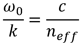
2nmc
"o = - -
^ef faring
Here, co represents the frequency of the optical signal, and mo represents the resonance frequency of the phase modulator. Also, Qo represents the intrinsic quality factor and Qc represents the coupling quality factor between the phase modulator and the signal pathway carrying the optical signal. The function 7(m) represents transmittance of the optical signal as a function of frequency, and T represents the complex coefficient of transmission. In addition, k represents a wavevector, m represents the mode order of the phase modulator, //^/ represents the effective index of refraction of the phase modulator, and Ling represents the length of the phase modulator. It is possible to control the phase modulator’s effective index of refraction (neff) and change it slightly, such as by altering the gap between the edge of the phase modulator and the signal pathway, the width of the signal pathway, and/or the coupling mode (such as TE versus TM modes) used to couple the optical signal into and out of the phase modulator.
[0075] As a result, these features can be used as noted above to control how a phase modulator affects the phase of optical signals traveling through one or more signal pathways. For example, with respect to FIGURES 7 through 10, one or more of these approaches can be used to ensure that the resonance peak of each phase modulator is identical or nearly identical for different wavelengths or wavelength ranges of optical signals in its associated signal pathways. With respect to FIGURE 11, one or more of these approaches can be used to ensure that the resonance peak of each phase modulator is identical or nearly identical for different wavelengths or wavelength ranges of optical signals in its associated signal pathway.
[0076] Note that the different wavelengths or wavelength bands mentioned above as being supported by the various unit cells 504 of the optical phased array 502 represent spectrally-distinct wavelengths or wavelength bands. In other words, these wavelengths or wavelength bands are separated by an adequate amount spectrally such that they can (if desired) be used simultaneously. As a result, for instance, optical signals carrying data can be transmitted and received while transmitting or receiving beacon optical signals. Moreover, the phase shifts provided to the optical signals in the spectrally-distinct wavelengths or wavelength bands by the structures shown in FIGURES 7 through 11 represent correlated phase shifts. That is, the phase shifts imparted to the optical signals can be substantially or completely equal, even though those optical signals are at or within the spectrally-distinct wavelengths or wavelength bands.
[0077] Although FIGURES 7 through 11 illustrate examples of multi -wavelength phase modulator networks, various changes may be made to FIGURES 7 through 11. For example, each multi -wavelength phase modulator network may include any suitable number of phase modulators, and each phase modulator may be associated with any suitable number of signal pathways coupled to any suitable number of antenna elements. Also, any suitable combination of features shown in FIGURES 7 through 11 could be used together in a single multi -wavelength phase modulator network, whether or not that specific combination of features is shown in the figures or described above. As a particular example, any of the multi -wavelength phase modulator networks described above may include pairs of antenna elements to support multi-polarization sensitivity. It is also possible to use combinations of some or all of the different arrangements of antenna elements and signal pathways from FIGURES 7 through 11 in a single multi -wavelength phase modulator network. In addition, while the phase modulators 706, 806, 906, 1006, 1106 are shown here as being annular structures, each phase modulator may have any other suitable design (such as a cloverleaf design).
[0078] FIGURES 12 and 13 illustrate example phase modulators for use in photonic integrated circuit multi -wavelength phase modulator networks according to this disclosure. In
particular, FIGURES 12 and 13 illustrate example phase modulators 706 that may be used in the unit cells 504 of the optical phased array 502. Note, however, that the same or similar type of structure may also or alternatively be used as any of the other phase modulators 806, 906, 1006, 1106 discussed above.
[0079] As shown in FIGURE 12, the phase modulator 706 here represents a thermal resonator that is implemented using a micro-ring resonator 1202 and a heater 1204 positioned above or otherwise near the micro-ring resonator 1202. The micro-ring resonator 1202 resonates based on one or more optical signals flowing through one or more associated signal pathways 704a-704b. Varying the temperature of the micro-ring resonator 1202 alters the resonance wavelength of the micro-ring resonator 1202, thereby changing the phase(s) of the optical signal(s) flowing through the signal pathway(s) 704a-704b. Voltages can be applied to two electrical contacts 1206 of the heater 1204 in order to create the desired temperature change and therefore implement the desired phase shift(s) of the optical signal(s) flowing through the signal pathway(s) 704a-704b. Different voltages applied to the heater 1204 can cause different phase shifts to occur in the phase modulator 706.
[0080] The micro-ring resonator 1202 may be formed from any suitable material(s), such as silicon, and in any suitable manner. The heater 1204 may be formed from any suitable material(s), such as one or more metals, and in any suitable manner. The micro-ring resonator 1202 may be separated from the heater 1204 by any suitable material(s), such as silicon dioxide. The micro-ring resonator 1202 and heater 1204 may each have any suitable size, shape, and dimensions. In some embodiments, the micro-ring resonator 1202 is annular and has a diameter of about 6 pm, and the heater 1204 is crescent-shaped and has a diameter of about 6 pm. However, other shapes and sizes may be used here. A gap 1208 between the micro-ring resonator 1202 and each signal pathway 704a-704b may have any suitable value, such as about 150 nm to about 210 nm (±10 nm). In some cases, design parameters like the thickness of the micro-ring resonator 1202 or the size of each gap 1208 can be altered in order to provide desired functionality for the phase modulator 706.
[0081] As shown in FIGURE 13, the phase modulator 706 here represents a PN junction micro-ring modulator that is implemented using various regions of semiconductor material, such as doped and undoped silicon. In this example, the phase modulator 706 is shown in cross-section for explanation. Here, the phase modulator 706 includes a first annular semiconductor region 1302 separated from a second annular semiconductor region 1304. The annular semiconductor regions 1302 and 1304 can represent different types of semiconductor material, such as when the annular semiconductor region 1302 represents an N-type semiconductor material and the annular
semiconductor region 1304 represents a P-type semiconductor material. A semiconductor region 1306 (such as undoped silicon) can separate the regions 1302-1304. A doped semiconductor region 1308 is positioned within the annular regions 1302-1304, and a doped semiconductor region 1310 is positioned around an upper portion of the doped semiconductor region 1308. The doped semiconductor regions 1308 and 1310 can represent different regions of semiconductor material with different dopants, such as when the doped semiconductor region 1308 is doped with an N+ dopant and the doped semiconductor region 1310 is doped with a P+ dopant. An electrical contact 1312 can be used to form an electrical connection with the doped semiconductor region 1308, and an electrical contact 1314 can be used to form an electrical connection with the doped semiconductor region 1310. An electrical connection 1316 can be used to provide a voltage to the electrical contact 1312, and an electrical connection 1318 can be used to provide a voltage to the electrical contact 1314.
[0082] Here, the various semiconductor regions 1302-1310 form a PN junction micro-ring modulator, and the electrical contacts 1312 and 1314 and electrical connections 1316 and 1318 allow voltages to be applied that alter the charge carrier density of the PN junction micro-ring modulator. This alters the phase of one or more optical signals flowing through one or more associated signal pathways 704a-704b. Voltages applied to the electrical connections 1316 and 1318 can provide the desired voltage difference and therefore implement the desired phase shift(s) of the optical signal(s) flowing through the signal pathway(s) 704a-704b. Different voltages applied to the electrical connections 1316 and 1318 can cause different phase shifts to occur in the phase modulator 706.
[0083] Although FIGURES 12 and 13 illustrate examples of phase modulators for use in photonic integrated circuit multi -wavelength phase modulator networks, various changes may be made to FIGURES 12 and 13. For example, the actual structure of a thermal resonator or PN junction micro-ring modulator can vary as needed or desired. Also, any other suitable structure may be used to phase-modulate one or more optical signals in the photonic integrated circuit 402 described above.
[0084] The following describes example embodiments of this disclosure that implement or relate to photonic integrated circuit multi -wavelength phase modulator networks. However, other embodiments may be used in accordance with the teachings of this disclosure.
[0085] In a first embodiment, an apparatus includes a photonic integrated circuit having an optical phased array, where the optical phased array includes multiple unit cells. Each unit cell includes at least one antenna element configured to transmit or receive multiple optical signals having spectrally-distinct wavelengths or wavelength ranges. Each unit cell also includes at least
one signal pathway configured to transport the optical signals to or from the at least one antenna element. Each unit cell further includes a phase modulator configured to modify phases of the optical signals being transported through the at least one signal pathway. Each unit cell is configured to provide correlated phase shifts to the optical signals having the spectrally-distinct wavelengths or wavelength ranges.
[0086] In a second embodiment, a method includes transmitting or receiving optical signals having spectrally-distinct wavelengths or wavelength ranges at a photonic integrated circuit having an optical phased array. The optical phased array includes multiple unit cells. The unit cells include (i) antenna elements configured to transmit or receive the optical signals, (ii) signal pathways configured to transport the optical signals to or from the antenna elements, and (iii) phase modulators configured to modify phases of the optical signals being transported through the signal pathways. The method also includes providing correlated phase shifts to the optical signals having the spectrally-distinct wavelengths or wavelength ranges using the unit cells.
[0087] In a third embodiment, an apparatus includes a photonic integrated circuit having an optical phased array, where the optical phased array includes multiple unit cells. Each unit cell includes means for transmitting or receiving multiple optical signals having spectrally-distinct wavelengths or wavelength ranges, means for transporting the optical signals to or from the at least one antenna element, and means for modifying phases of the optical signals being transported through the at least one signal pathway. Each unit cell is configured to provide correlated phase shifts to the optical signals having the spectrally-distinct wavelengths or wavelength ranges.
[0088] Any single one or any suitable combination of the following features may be used with the first, second, or third embodiment. The optical signals may include optical signals having at least two spectrally-distinct wavelengths or wavelength ranges, and each unit cell may have a modulator bandwidth that includes the at least two spectrally-distinct wavelengths or wavelength ranges. The optical signals may include optical signals having at least two spectrally-distinct wavelengths or wavelength ranges, the phase modulator of each unit cell may have a free spectral range, and each spectrally-distinct wavelength or wavelength range may be separated from at least one adjacent spectrally-distinct wavelength or wavelength range by the free spectral range. Each unit cell may include multiple antenna elements and multiple signal pathways, where each signal pathway may be coupled to one of the antenna elements and pass along a portion of an edge of the phase modulator. Each unit cell may include multiple pairs of antenna elements and multiple signal pathways, where each pair of antenna elements may include two orthogonally-arranged antenna elements and where each signal pathway may be coupled to one of the pairs of antenna elements and pass along a portion of an edge of the phase modulator. Each unit cell may include a single
antenna element, multiple signal pathways (where each signal pathway may pass along a portion of an edge of the phase modulator), and a wavelength splitter/combiner coupling the single antenna element and the multiple signal pathways. Each unit cell may include a single antenna element and a single signal pathway passing along a portion of an edge of the phase modulator. In each unit cell, the phase modulator may have peak resonances associated with the spectrally-distinct wavelengths or wavelength ranges that are equal or substantially equal. In each unit cell, gaps between edges of the phase modulator and multiple signal pathways may be different; widths of multiple signal pathways may be different; arc lengths of multiple signal pathways along a curved edge of the phase modulator may be different; and/or coupling modes used to couple the optical signals having the spectrally-distinct wavelengths or wavelength ranges into and out of the phase modulator may be different. In each unit cell, the phase modulator may include a micro-ring resonator and a heater, and the heater may be configured to change a refractive index of the microring resonator.
[0089] In some embodiments, various functions described in this patent document are implemented or supported by a computer program that is formed from computer readable program code and that is embodied in a computer readable medium. The phrase “computer readable program code” includes any type of computer code, including source code, object code, and executable code. The phrase “computer readable medium” includes any type of medium capable of being accessed by a computer, such as read only memory (ROM), random access memory (RAM), a hard disk drive (HDD), a compact disc (CD), a digital video disc (DVD), or any other type of memory. A “non-transitory” computer readable medium excludes wired, wireless, optical, or other communication links that transport transitory electrical or other signals. A non-transitory computer readable medium includes media where data can be permanently stored and media where data can be stored and later overwritten, such as a rewritable optical disc or an erasable storage device.
[0090] It may be advantageous to set forth definitions of certain words and phrases used throughout this patent document. The terms “application” and “program” refer to one or more computer programs, software components, sets of instructions, procedures, functions, objects, classes, instances, related data, or a portion thereof adapted for implementation in a suitable computer code (including source code, object code, or executable code). The term “communicate,” as well as derivatives thereof, encompasses both direct and indirect communication. The terms “include” and “comprise,” as well as derivatives thereof, mean inclusion without limitation. The term “or” is inclusive, meaning and/or. The phrase “associated with,” as well as derivatives thereof, may mean to include, be included within, interconnect with, contain, be contained within, connect
to or with, couple to or with, be communicable with, cooperate with, interleave, juxtapose, be proximate to, be bound to or with, have, have a property of, have a relationship to or with, or the like. The phrase “at least one of,” when used with a list of items, means that different combinations of one or more of the listed items may be used, and only one item in the list may be needed. For example, “at least one of: A, B, and C” includes any of the following combinations: A, B, C, A and B, A and C, B and C, and A and B and C.
[0091] The description in the present disclosure should not be read as implying that any particular element, step, or function is an essential or critical element that must be included in the claim scope. The scope of patented subject matter is defined only by the allowed claims. Moreover, none of the claims invokes 35 U.S.C. § 112(f) with respect to any of the appended claims or claim elements unless the exact words “means for” or “step for” are explicitly used in the particular claim, followed by a participle phrase identifying a function. Use of terms such as (but not limited to) “mechanism,” “module,” “device,” “unit,” “component,” “element,” “member,” “apparatus,” “machine,” “system,” “processor,” or “controller” within a claim is understood and intended to refer to structures known to those skilled in the relevant art, as further modified or enhanced by the features of the claims themselves, and is not intended to invoke 35 U.S.C. § 112(f).
[0092] While this disclosure has described certain embodiments and generally associated methods, alterations and permutations of these embodiments and methods will be apparent to those skilled in the art. Accordingly, the above description of example embodiments does not define or constrain this disclosure. Other changes, substitutions, and alterations are also possible without departing from the spirit and scope of this disclosure, as defined by the following claims.
Claims
1. An apparatus comprising: a photonic integrated circuit comprising an optical phased array, the optical phased array comprising multiple unit cells, each unit cell comprising: at least one antenna element configured to transmit or receive multiple optical signals having spectrally-distinct wavelengths or wavelength ranges; at least one signal pathway configured to transport the optical signals to or from the at least one antenna element; and a phase modulator configured to modify phases of the optical signals being transported through the at least one signal pathway; wherein each unit cell is configured to provide correlated phase shifts to the optical signals having the spectrally-distinct wavelengths or wavelength ranges.
2. The apparatus of Claim 1, wherein: the optical signals comprise optical signals having at least two spectrally-distinct wavelengths or wavelength ranges; and each unit cell has a modulator bandwidth that includes the at least two spectrally-distinct wavelengths or wavelength ranges.
3. The apparatus of Claim 1, wherein: the optical signals comprise optical signals having at least two spectrally-distinct wavelengths or wavelength ranges; the phase modulator of each unit cell has a free spectral range; and each spectrally-distinct wavelength or wavelength range is separated from at least one adjacent spectrally-distinct wavelength or wavelength range by the free spectral range.
4. The apparatus of Claim 1, wherein each unit cell comprises: multiple antenna elements; and multiple signal pathways, each signal pathway coupled to one of the antenna elements and passing along a portion of an edge of the phase modulator.
5. The apparatus of Claim 1, wherein each unit cell comprises: multiple pairs of antenna elements, each pair of antenna elements comprising two orthogonally-arranged antenna elements; and
multiple signal pathways, each signal pathway coupled to one of the pairs of antenna elements and passing along a portion of an edge of the phase modulator.
6. The apparatus of Claim 1, wherein each unit cell comprises: a single antenna element; multiple signal pathways, each signal pathway passing along a portion of an edge of the phase modulator; and a wavelength splitter/combiner coupling the single antenna element and the multiple signal pathways.
7. The apparatus of Claim 1, wherein each unit cell comprises: a single antenna element; and a single signal pathway passing along a portion of an edge of the phase modulator.
8. The apparatus of Claim 1, wherein, in each unit cell, the phase modulator has peak resonances associated with the spectrally-distinct wavelengths or wavelength ranges that are equal or substantially equal.
9. The apparatus of Claim 1, wherein, in each unit cell, at least one of: gaps between edges of the phase modulator and multiple signal pathways are different; widths of multiple signal pathways are different; arc lengths of multiple signal pathways along a curved edge of the phase modulator are different; and coupling modes used to couple the optical signals having the spectrally-distinct wavelengths or wavelength ranges into and out of the phase modulator are different.
10. The apparatus of Claim 1, wherein, in each unit cell, the phase modulator comprises a micro-ring resonator and a heater, the heater configured to change a refractive index of the microring resonator.
11. A method comprising: transmitting or receiving optical signals having spectrally-distinct wavelengths or wavelength ranges at a photonic integrated circuit comprising an optical phased array, the optical phased array comprising multiple unit cells, the unit cells comprising (i) antenna elements
configured to transmit or receive the optical signals, (ii) signal pathways configured to transport the optical signals to or from the antenna elements, and (iii) phase modulators configured to modify phases of the optical signals being transported through the signal pathways; and providing correlated phase shifts to the optical signals having the spectrally-distinct wavelengths or wavelength ranges using the unit cells.
12. The method of Claim 11, wherein: the optical signals comprise optical signals having at least two spectrally-distinct wavelengths or wavelength ranges; and each unit cell has a modulator bandwidth that includes the at least two spectrally-distinct wavelengths or wavelength ranges.
13. The method of Claim 11, wherein: the optical signals comprise optical signals having at least two spectrally-distinct wavelengths or wavelength ranges; the phase modulator of each unit cell has a free spectral range; and each spectrally-distinct wavelength or wavelength range is separated from at least one adjacent spectrally-distinct wavelength or wavelength range by the free spectral range.
14. The method of Claim 11, wherein each unit cell comprises: multiple antenna elements; and multiple signal pathways, each signal pathway coupled to one of the antenna elements and passing along a portion of an edge of the phase modulator.
15. The method of Claim 11, wherein each unit cell comprises: multiple pairs of antenna elements, each pair of antenna elements comprising two orthogonally-arranged antenna elements; and multiple signal pathways, each signal pathway coupled to one of the pairs of antenna elements and passing along a portion of an edge of the phase modulator.
16. The method of Claim 11, wherein each unit cell comprises: a single antenna element; multiple signal pathways, each signal pathway passing along a portion of an edge of the phase modulator; and
a wavelength splitter/combiner coupling the single antenna element and the multiple signal pathways.
17. The method of Claim 11, wherein each unit cell comprises: a single antenna element; and a single signal pathway passing along a portion of an edge of the phase modulator.
18. The method of Claim 11, wherein, in each unit cell, the phase modulator has peak resonances associated with the spectrally-distinct wavelengths or wavelength ranges that are equal or substantially equal.
19. The method of Claim 11, wherein, in each unit cell, at least one of: gaps between edges of the phase modulator and multiple signal pathways are different; widths of multiple signal pathways are different; arc lengths of multiple signal pathways along a curved edge of the phase modulator are different; and coupling modes used to couple the optical signals having the spectrally-distinct wavelengths or wavelength ranges into and out of the phase modulator are different.
20. An apparatus comprising: a photonic integrated circuit comprising an optical phased array, the optical phased array comprising multiple unit cells, each unit cell comprising: means for transmitting or receiving multiple optical signals having spectrally- distinct wavelengths or wavelength ranges; means for transporting the optical signals to or from the at least one antenna element; and means for modifying phases of the optical signals being transported through the at least one signal pathway; wherein each unit cell is configured to provide correlated phase shifts to the optical signals having the spectrally-distinct wavelengths or wavelength ranges.
Applications Claiming Priority (2)
| Application Number | Priority Date | Filing Date | Title |
|---|---|---|---|
| US17/806,873 US12189180B2 (en) | 2022-06-14 | 2022-06-14 | Photonic integrated circuit multi-wavelength phase modulator networks |
| US17/806,873 | 2022-06-14 |
Publications (1)
| Publication Number | Publication Date |
|---|---|
| WO2023244875A1 true WO2023244875A1 (en) | 2023-12-21 |
Family
ID=85772096
Family Applications (1)
| Application Number | Title | Priority Date | Filing Date |
|---|---|---|---|
| PCT/US2023/063127 Ceased WO2023244875A1 (en) | 2022-06-14 | 2023-02-23 | Photonic integrated circuit multi-wavelength phase modulator networks |
Country Status (2)
| Country | Link |
|---|---|
| US (1) | US12189180B2 (en) |
| WO (1) | WO2023244875A1 (en) |
Citations (2)
| Publication number | Priority date | Publication date | Assignee | Title |
|---|---|---|---|---|
| US20190068282A1 (en) * | 2016-03-23 | 2019-02-28 | The Boeing Company | High-Capacity Communications Satellite Using Passive Optical Beamforming |
| US20190391243A1 (en) * | 2017-03-01 | 2019-12-26 | Pointcloud Inc. | Modular three-dimensional optical sensing system |
Family Cites Families (32)
| Publication number | Priority date | Publication date | Assignee | Title |
|---|---|---|---|---|
| US3975628A (en) | 1975-04-02 | 1976-08-17 | Hughes Aircraft Company | Optical heterodyne receiver with phase or frequency lock |
| US7949030B2 (en) | 2005-02-03 | 2011-05-24 | Pd-Ld, Inc. | High-power, phased-locked, laser arrays |
| US7408507B1 (en) | 2005-03-15 | 2008-08-05 | The United States Of America As Represented By The Secretary Of The Navy | Antenna calibration method and system |
| US20060239312A1 (en) | 2005-04-23 | 2006-10-26 | Telaris Inc. | Semiconductor Lasers in Optical Phase-Locked Loops |
| US8068235B1 (en) | 2007-07-24 | 2011-11-29 | Lockheed Martin Corporation | Systems and methods for multi-function coherent imaging |
| US7729572B1 (en) | 2008-07-08 | 2010-06-01 | Hrl Laboratories, Llc | Optical tapped time delay modules and arrays |
| US9476981B2 (en) | 2013-01-08 | 2016-10-25 | Massachusetts Institute Of Technology | Optical phased arrays |
| US10132928B2 (en) | 2013-05-09 | 2018-11-20 | Quanergy Systems, Inc. | Solid state optical phased array lidar and method of using same |
| US11038268B2 (en) * | 2013-08-30 | 2021-06-15 | Telefonaktiebolaget Lm Ericsson (Publ) | Signal generator for a phased array antenna |
| US20160094016A1 (en) | 2014-09-30 | 2016-03-31 | Lawrence Livermore National Security, Llc | Increasing the spatial and spectral brightness of laser diode arrays |
| US10598785B2 (en) | 2016-02-11 | 2020-03-24 | California Institute Of Technology | Hybrid transmitter receiver optical imaging system |
| US11456532B2 (en) * | 2016-05-04 | 2022-09-27 | California Institute Of Technology | Modular optical phased array |
| US10634973B2 (en) * | 2016-08-02 | 2020-04-28 | University Of Southern California | Two-dimensional optical phased array |
| WO2018128662A2 (en) | 2016-10-14 | 2018-07-12 | Analog Photonics LLC | Large scale optical phased array |
| US9740079B1 (en) * | 2016-10-28 | 2017-08-22 | National Technology & Engineering Solutions Of Sandia, Llc | Integrated optical transceiver with electronically controlled optical beamsteering |
| US10591802B2 (en) * | 2018-01-18 | 2020-03-17 | Litexel Inc. | On-chip optical phased array using a serial grating antenna design |
| US10838222B2 (en) | 2018-02-12 | 2020-11-17 | California Institute Of Technology | Coherence artifacts suppression in integrated photonic systems |
| EP3761528B1 (en) | 2018-04-27 | 2022-08-31 | Mitsubishi Electric Corporation | Space optical communication device |
| US11249370B2 (en) | 2018-12-18 | 2022-02-15 | California Institute Of Technology | Optical phased arrays and methods for calibrating and focusing of optical phased arrays |
| US10790909B1 (en) | 2019-05-09 | 2020-09-29 | Lockheed Martin Corporation | Efficient multi-channel coherent optical system |
| KR102200681B1 (en) | 2019-09-02 | 2021-01-11 | 한국과학기술원 | Device system for constituting 3d image sensor capable of wireless data transmission and reception based on optical phased array |
| KR102739954B1 (en) | 2019-11-20 | 2024-12-09 | 삼성전자주식회사 | Beam steering apparatus and system |
| US11029465B1 (en) | 2020-03-27 | 2021-06-08 | Globalfoundries U.S. Inc. | Micro-ring modulator |
| US12050341B2 (en) | 2020-07-15 | 2024-07-30 | Raytheon Company | Photonic integrated circuit distance measuring interferometer |
| US11940621B2 (en) * | 2020-09-04 | 2024-03-26 | Analog Photonics LLC | Two dimensional optical phased arrays using edge-coupled integrated circuits |
| US11664894B2 (en) | 2021-01-11 | 2023-05-30 | Raytheon Company | Photonic integrated circuit-based optical phased array communication system |
| US11703739B2 (en) | 2021-01-15 | 2023-07-18 | Raytheon Company | System and method for calibrating PIC-based optical phased array transmitter and receiver |
| US11934048B2 (en) | 2021-01-29 | 2024-03-19 | Raytheon Company | Photonic integrated circuit-based coherently phased array laser transmitter |
| US11988903B2 (en) | 2021-02-11 | 2024-05-21 | Raytheon Company | Photonic integrated circuit-based optical phased array calibration technique |
| US11644621B2 (en) | 2021-02-11 | 2023-05-09 | Raytheon Company | Digital input circuit design for photonic integrated circuit |
| US11532881B2 (en) | 2021-02-11 | 2022-12-20 | Raytheon Company | Photonic integrated circuit-based optical phased array phasing technique |
| US11476576B2 (en) | 2021-02-11 | 2022-10-18 | Raytheon Company | Photonic integrated circuit-based communication transmit/receive system |
-
2022
- 2022-06-14 US US17/806,873 patent/US12189180B2/en active Active
-
2023
- 2023-02-23 WO PCT/US2023/063127 patent/WO2023244875A1/en not_active Ceased
Patent Citations (2)
| Publication number | Priority date | Publication date | Assignee | Title |
|---|---|---|---|---|
| US20190068282A1 (en) * | 2016-03-23 | 2019-02-28 | The Boeing Company | High-Capacity Communications Satellite Using Passive Optical Beamforming |
| US20190391243A1 (en) * | 2017-03-01 | 2019-12-26 | Pointcloud Inc. | Modular three-dimensional optical sensing system |
Also Published As
| Publication number | Publication date |
|---|---|
| US12189180B2 (en) | 2025-01-07 |
| US20230400628A1 (en) | 2023-12-14 |
Similar Documents
| Publication | Publication Date | Title |
|---|---|---|
| US11988903B2 (en) | Photonic integrated circuit-based optical phased array calibration technique | |
| US11476576B2 (en) | Photonic integrated circuit-based communication transmit/receive system | |
| US11532881B2 (en) | Photonic integrated circuit-based optical phased array phasing technique | |
| US11644621B2 (en) | Digital input circuit design for photonic integrated circuit | |
| JP7247257B2 (en) | How to store data in motion | |
| US11962350B2 (en) | Photonic integrated circuit with independent unit cells having multi-polarization sensitivity | |
| US11934048B2 (en) | Photonic integrated circuit-based coherently phased array laser transmitter | |
| US12261645B2 (en) | Multi-node, multi-stream photonic integrated circuit-based free-space optical communication device | |
| US12088343B2 (en) | Photonic integrated circuit-based polarization-independent optical devices | |
| US11716141B1 (en) | Photonic integrated circuit-based optical communication optimized for receive aperture amplitude and phase modulations | |
| US20230417985A1 (en) | Photonic integrated circuit temporal and frequency dispersion squint correction for optical phased array | |
| US11962346B2 (en) | Photonic integrated circuit (PIC)-based optical phased array with integrated gyroscopic sensor | |
| US12189180B2 (en) | Photonic integrated circuit multi-wavelength phase modulator networks | |
| US11894873B2 (en) | Photonic integrated circuit with inverted H-tree unit cell design | |
| US11888515B1 (en) | System and method for parallel real-time photonic integrated circuit (PIC) optical phased array calibration and ultraviolet laser micro-ring wavelength offset trimming | |
| Kohtoku | Compact InP-based optical modulator for 100-Gb/s coherent pluggable transceivers | |
| Fathololoumi et al. | Photonic-integrated circuits for switched network interconnects | |
| US12164146B2 (en) | Photonic integrated circuit-based transmissive/reflective wavefront optical phase control | |
| US20240162989A1 (en) | Integrated photonic integrated circuit (pic) and readout integrated circuit (roic) for high-speed data output from focal plane array | |
| Gunn | CMOS photonics technology overview |
Legal Events
| Date | Code | Title | Description |
|---|---|---|---|
| 121 | Ep: the epo has been informed by wipo that ep was designated in this application |
Ref document number: 23713237 Country of ref document: EP Kind code of ref document: A1 |
|
| NENP | Non-entry into the national phase |
Ref country code: DE |
|
| 122 | Ep: pct application non-entry in european phase |
Ref document number: 23713237 Country of ref document: EP Kind code of ref document: A1 |