WO2023243351A1 - 弾性波装置、および通信装置 - Google Patents
弾性波装置、および通信装置 Download PDFInfo
- Publication number
- WO2023243351A1 WO2023243351A1 PCT/JP2023/019449 JP2023019449W WO2023243351A1 WO 2023243351 A1 WO2023243351 A1 WO 2023243351A1 JP 2023019449 W JP2023019449 W JP 2023019449W WO 2023243351 A1 WO2023243351 A1 WO 2023243351A1
- Authority
- WO
- WIPO (PCT)
- Prior art keywords
- wave device
- elastic wave
- region
- low sound
- sound velocity
- Prior art date
- Legal status (The legal status is an assumption and is not a legal conclusion. Google has not performed a legal analysis and makes no representation as to the accuracy of the status listed.)
- Ceased
Links
Images


Classifications
-
- H—ELECTRICITY
- H03—ELECTRONIC CIRCUITRY
- H03H—IMPEDANCE NETWORKS, e.g. RESONANT CIRCUITS; RESONATORS
- H03H9/00—Networks comprising electromechanical or electro-acoustic elements; Electromechanical resonators
- H03H9/02—Details
- H03H9/125—Driving means, e.g. electrodes, coils
- H03H9/145—Driving means, e.g. electrodes, coils for networks using surface acoustic waves
-
- H—ELECTRICITY
- H03—ELECTRONIC CIRCUITRY
- H03H—IMPEDANCE NETWORKS, e.g. RESONANT CIRCUITS; RESONATORS
- H03H9/00—Networks comprising electromechanical or electro-acoustic elements; Electromechanical resonators
- H03H9/25—Constructional features of resonators using surface acoustic waves
Definitions
- Patent Document 1 discloses an example of the configuration of an elastic wave device having a membrane structure.
- FIG. 7 is a cross-sectional view of an elastic wave device according to a fourth embodiment.
- 12 is a graph showing a transverse mode index according to the amount of silicon penetration in the elastic wave device according to the fourth embodiment. It is a phase average value from the resonance frequency to the anti-resonance frequency according to the amount of silicon penetration in the elastic wave device according to the fourth embodiment. 12 is a graph showing a transverse mode index according to the amount of silicon penetration in the elastic wave device according to the fifth embodiment.
- FIG. 29 is a plan view of one cycle of the IDT electrode 600 in the general acoustic wave device 100. Therefore, the IDT electrodes 600 are arranged in the electrode finger arrangement direction (Y direction).
- FIG. 30 is a cross-sectional view of a general elastic wave device 100.
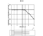
- FIG. 31 is a diagram showing frequency characteristics of a general elastic wave device 100 according to Comparative Example 1.
- the horizontal axis represents frequency and the vertical axis represents phase.
- the phase may be constant at 90°.
- Comparative Example 2 Frequency characteristics when silicon 3 invades below the IDT electrode 600
- the cavity 4 is smaller than that of the elastic wave device 100, and the silicon 3 penetrates below the IDT electrode 600. That is, the outer edge 4a of the cavity 4 is located below the IDT electrode 600.
- the duty of the electrode fingers is constant from the root to the tip.
- the dummy electrode fingers also have the same duty as the electrode fingers.
- Such an elastic wave device is also called a non-duty offset resonator or a normal resonator.
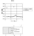
- FIG. 32 is a diagram showing the frequency characteristics of the elastic wave device according to Comparative Example 2.
- the horizontal axis represents frequency and the vertical axis represents phase.
- the solid line is the frequency characteristic when silicon 3 penetrates below the IDT electrode 600 in the acoustic wave device according to Comparative Example 2, and the broken line shows the frequency characteristic when silicon 3 penetrates below the IDT electrode 600 in the acoustic wave device according to Comparative Example 2. This is the frequency characteristic when it does not penetrate below .
- the schematic diagram at the bottom of FIG. 32 is a schematic diagram showing the amount of silicon 3 infiltrated. In the case of the solid line, the amount of penetration of silicon 3 is 0.5 ⁇ m. 0.5 ⁇ m corresponds to 1/3 of the thickness of the bus bar.
- FIG. 1 is a plan view of a part of the elastic wave device 1 according to the first embodiment.
- the elastic wave device 1 differs from the elastic wave device 100 in that an IDT electrode 6 is formed instead of the IDT electrode 600.
- the IDT electrode 6 includes a busbar 61a and a busbar 61b, an electrode finger 62a and an electrode finger 62b, a dummy electrode finger 63a and a dummy electrode finger 63b, and widened portions 65a and 65b (also called widened portion 65), to which different potentials are applied. ) and.
- the widened portion 65 is located near the bus bar 61 in the first region 60 .
- the widened portion 65 located near the bus bar 61 may exist within one wavelength from the end of the intersection region 64 on the bus bar side, or within a range of the pitch PT.
- widened portions 65 and dummy electrode fingers 63 are alternately connected to the bus bar 61, and electrode fingers 62 are connected to the widened portions 65.
- the fact that the electrode finger 62 and the dummy electrode finger 63 face each other remains unchanged.
- the ratio of the width to the pitch PT of the widened portion 65 is referred to as an offset duty OD, and the offset duty OD is larger than the duty D. That is, the width of the widened portion 65 in the Y direction (the direction in which the electrode fingers are arranged) is larger (widened) than the width of the electrode finger 62 in the Y direction. Further, the length of the widened portion 65 in the X direction (the direction in which the electrode finger extends) is longer than the length of the dummy electrode finger 63.
- the IDT electrode 6 having such a widened portion 65 is referred to as a duty offset resonator. Further, the dummy electrode finger (second electrode finger) 63 has a width larger than the average width of the electrode finger 62.
- a region extending in the direction in which the electrode fingers 62 are arranged in the width of the widened portion 65 is referred to as a low sound velocity region 66. Since the offset duty OD of the widened portion 65 is larger than the duty D of the electrode finger 62, the widened portion 65 has a larger weight per unit area than the electrode finger 62. Therefore, the sound speed in the low sound speed region 66 is low in the first region 60.
- FIG. 2 is a cross-sectional view of the elastic wave device 1 according to the first embodiment.
- silicon 3 has invaded below the IDT electrode 6.
- This amount of intrusion is defined as the amount of silicon intrusion x, where x is the distance from the end of the bus bar 61 outside the first region 60 to the outer edge 4a of the cavity 4.
- the silicon penetration amount x is a variable, and the frequency characteristics of the elastic wave device were simulated while adjusting the silicon penetration amount x.
- the duty D was 0.5 and the offset duty OD was 0.6.
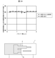
- FIGS. 3 to 7 In the upper graphs of FIGS. 3 to 7, the broken lines represent the frequency characteristics in the case of Comparative Example 1, and the solid lines represent the respective cases.
- the schematic diagrams at the bottom of FIGS. 3 to 7 are schematic diagrams showing the amount of silicon 3 infiltrated. As shown in FIGS. 3 to 7, the frequency characteristics change depending on the amount x of silicon 3 that penetrates below the IDT electrode 6.
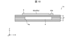
- FIG. 10 is a cross-sectional view of the elastic wave device 1a according to the second embodiment.
- the elastic wave device 1a differs from the elastic wave device 1 in that a connection layer 7a of silicon dioxide (SiO 2 ) is provided between the silicon 3 and the piezoelectric substrate 5.
- the connection layer 7a exists only above the silicon 3 and does not exist at the position of the cavity 4.
- the connection layer 7a has a thickness of about 0.1 ⁇ m.
- FIG. 13 is a cross-sectional view of an elastic wave device 1b according to the third embodiment.
- the elastic wave device 1b differs from the elastic wave device 1 in that a low resistance connection layer 7b is provided between the silicon 3 and the piezoelectric substrate 5.
- the connection layer 7b exists only above the silicon 3 and does not exist at the position of the cavity 4.
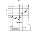
- the transverse mode index T is sufficiently small compared to Comparative Example 1 until the position of the outer edge 4a is located at the end of the low sound velocity region 66.
- the phase average value is also sufficiently close to 90° until the position of the outer edge 4a is located at the end of the low sound velocity region 66. Therefore, in the elastic wave device 1c according to the fourth embodiment, it can be said that the frequency characteristics are sufficiently good until the position of the outer edge 4a is located at the end of the low sound velocity region 66.
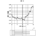
- the transverse mode index T is sufficiently small compared to Comparative Example 1 until the position of the outer edge 4a is located at the end of the low sound velocity region 66.
- the phase average value is also sufficiently close to 90° until the position of the outer edge 4a is located at the end of the low sound velocity region 66. Therefore, in the elastic wave device according to the fifth embodiment, it can be said that the frequency characteristics are sufficiently good until the position of the outer edge 4a is located at the end of the low sound velocity region 66.
- Embodiments 1 and 5 are the same except for the value of the offset duty OD, and good frequency characteristics could be obtained even if the offset duty OD was increased.
- the offset duty OD of the IDT electrode 6 is increased to 0.8 compared to the elastic wave device 1. In other words, the weight of the low sound velocity region 66 is increased.
- FIG. 21 is a graph showing the transverse mode index T according to the silicon penetration amount x in the elastic wave device according to the sixth embodiment.
- FIG. 22 shows the phase average value from the resonant frequency fr to the anti-resonant frequency fa according to the amount x of silicon penetration in the elastic wave device according to the sixth embodiment.
- the broken lines in FIGS. 21 and 22 are the values in Comparative Example 1, and the solid lines are the values in the elastic wave device according to the fifth embodiment.
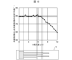
- FIG. 23 is a graph showing the transverse mode index T according to the width of the bus bar in the elastic wave device 1 according to the seventh embodiment.
- FIG. 24 shows phase average values from the resonant frequency fr to the anti-resonant frequency fa according to the width of the bus bar in the elastic wave device 1 according to the seventh embodiment.
- the silicon penetration amount x was assumed to be located below the tip of the dummy electrode finger 63.
- FIG. 25 is a plan view of the elastic wave device according to the eighth embodiment.
- the elastic wave device includes an IDT electrode 6f that is a piston resonator instead of the IDT electrode 6.
- the root of the electrode finger 62 in contact with the bus bar 61 and the tip of the electrode finger 62 are widened, and are a widened part 65 and a widened part 67, respectively. Further, the piston resonator does not include dummy electrode fingers 63. Furthermore, the bus bar 61 is provided with an opening 68 . The widened portion 67 and the opening 68 are classified into a widened portion 67a and a widened portion 67b, and an opening 68a and an opening 68b, depending on the applied potential.
- FIG. 28 is a diagram illustrating a schematic configuration of the communication device 151 in the ninth embodiment.
- the communication device 151 is an application example of an elastic wave device according to one aspect of the present disclosure, and performs wireless communication using radio waves.
- the communication device 151 may include one duplexer 101 as a transmission filter 109 and another duplexer 101 as a reception filter 111.
- Each of the two duplexers 101 may include an elastic wave device (eg, elastic wave device 1, 1a to 1f) according to one aspect of the present disclosure. In this way, the communication device 151 may include an elastic wave device according to one aspect of the present disclosure.
- a transmission information signal TIS containing information to be transmitted is modulated and frequency-increased (converted to a high-frequency signal having a carrier frequency) by an RF-IC (Radio Frequency-Integrated Circuit) 153, and the transmission information signal TIS is converted into a transmission signal. It may be converted to TS.
- the bandpass filter 155 may remove unnecessary components other than the transmission passband for the TS.
- the TS after removing unnecessary components may be amplified by the amplifier 157 and input to the transmission filter 109.
- the transmission filter 109 may remove unnecessary components outside the transmission passband from the input transmission signal TS.
- the transmission filter 109 may output the TS from which unnecessary components have been removed to the antenna 159 via an antenna terminal (eg, TCin described above).
- the antenna 159 may convert the TS, which is an electrical signal input to itself, into a radio wave as a wireless signal, and transmit the radio wave to the outside of the communication device 151.
- the antenna 159 may convert the received radio waves from the outside into a reception signal RS, which is an electrical signal, and input the RS to the reception filter 111 via the antenna terminal.
- the reception filter 111 may remove unnecessary components other than the reception passband from the input RS.
- the reception filter 111 may output the reception signal RS from which unnecessary components have been removed to the amplifier 161.
- the output RS may be amplified by the amplifier 161.
- the bandpass filter 163 may remove unnecessary components other than the receiving passband from the amplified RS.
- the frequency of the RS after unnecessary component removal is lowered and demodulated by the RF-IC 153, and may be converted into a received information signal RIS.
- the TIS and RIS may be low frequency signals (baseband signals) containing appropriate information.
- TIS and RIS may be analog audio signals or digitized audio signals.
- the passband of the wireless signal may be set as appropriate and may conform to various known standards.
- the low sound velocity region 66 was defined by the length of the widened portion 65 in the extending direction of the electrode fingers, but this is not the case. Specifically, the low sound velocity region 66 may be defined by adding an additional film to the electrode finger 62 instead of the widened portion 65 to increase the weight of at least a portion of the electrode finger 62. good. That is, the frequency characteristics of the elastic wave device may be improved by creating a low sound velocity region 66 in which the weight per unit length of the electrode finger is increased.
- An elastic wave device includes: a support substrate in which a cavity is formed; a piezoelectric substrate located on the support substrate and covering the cavity; and a piezoelectric substrate located on the piezoelectric substrate.
- an IDT electrode the IDT electrode has a pair of bus bars and a plurality of electrode fingers provided in a first region sandwiched between the pair of bus bars, and an intersection region in the first region. is arranged so as to overlap the hollow portion in plan view, and the first region has a higher elasticity in the arrangement direction of the plurality of electrode fingers than at least some other regions in the first region.
- the area includes a low sound speed area extending in the arrangement direction, where the sound speed of waves is low, and the outer edge of the cavity portion and the low sound speed area overlap in plan view.
- the low sound velocity region may be configured by providing a widened portion in the plurality of electrode fingers.
- the electrode finger may have a low sound velocity region, and the low sound velocity region is widened.
- the low sound velocity region may be configured by providing an additional film on the plurality of electrode fingers.
- the electrode finger may have a low sound velocity region, and the low sound velocity region has an additional film.
- the low sound velocity region faces the electrode fingers in the extending direction of the electrode fingers, and has an average width of the electrode fingers.
- the second electrode finger may be provided with a width larger than that of the second electrode finger.
- the second electrode finger may be provided as the low sound velocity region.
- the low sound velocity region may be a part of the region near the pair of bus bars.
- the low sound velocity region can be located near the bus bar.
- the widened portion may be provided on the tip side of the electrode finger.
- the low sound velocity region can be located on the tip side of the electrode finger.
- the distance from the low sound velocity region to the intersection region may be within one wavelength.
- the distance from the low sound velocity region to the crossing region is within the attachment pitch of the plurality of electrode fingers. Good too.
- the low sound velocity region can exist up to the vicinity of the intersection region.
- the bus bar may be configured by providing a gap.
- the support substrate may be made of silicon.
- silicon can be used as the support substrate.
- the IDT electrode may excite an elastic wave of an A1 moderam wave.
- the IDT electrode can excite the elastic wave of the A1 moderam wave.
- the elastic wave device according to aspect 12 of the present disclosure may be a communication device including the elastic wave device in any one of aspects 1 to 11.
- the communication device can be filtered by the elastic wave device.
Landscapes
- Physics & Mathematics (AREA)
- Acoustics & Sound (AREA)
- Surface Acoustic Wave Elements And Circuit Networks Thereof (AREA)
Priority Applications (1)
| Application Number | Priority Date | Filing Date | Title |
|---|---|---|---|
| JP2024528643A JPWO2023243351A1 (https=) | 2022-06-17 | 2023-05-25 |
Applications Claiming Priority (2)
| Application Number | Priority Date | Filing Date | Title |
|---|---|---|---|
| JP2022098302 | 2022-06-17 | ||
| JP2022-098302 | 2022-06-17 |
Publications (1)
| Publication Number | Publication Date |
|---|---|
| WO2023243351A1 true WO2023243351A1 (ja) | 2023-12-21 |
Family
ID=89191206
Family Applications (1)
| Application Number | Title | Priority Date | Filing Date |
|---|---|---|---|
| PCT/JP2023/019449 Ceased WO2023243351A1 (ja) | 2022-06-17 | 2023-05-25 | 弾性波装置、および通信装置 |
Country Status (2)
| Country | Link |
|---|---|
| JP (1) | JPWO2023243351A1 (https=) |
| WO (1) | WO2023243351A1 (https=) |
Citations (4)
| Publication number | Priority date | Publication date | Assignee | Title |
|---|---|---|---|---|
| WO2019003909A1 (ja) * | 2017-06-26 | 2019-01-03 | 株式会社村田製作所 | 弾性波装置及び複合フィルタ装置 |
| WO2020100949A1 (ja) * | 2018-11-14 | 2020-05-22 | 京セラ株式会社 | 弾性波装置、分波器および通信装置 |
| WO2022045307A1 (ja) * | 2020-08-28 | 2022-03-03 | 京セラ株式会社 | 弾性波素子及び通信装置 |
| WO2022102720A1 (ja) * | 2020-11-13 | 2022-05-19 | 株式会社村田製作所 | 弾性波装置 |
-
2023
- 2023-05-25 WO PCT/JP2023/019449 patent/WO2023243351A1/ja not_active Ceased
- 2023-05-25 JP JP2024528643A patent/JPWO2023243351A1/ja active Pending
Patent Citations (4)
| Publication number | Priority date | Publication date | Assignee | Title |
|---|---|---|---|---|
| WO2019003909A1 (ja) * | 2017-06-26 | 2019-01-03 | 株式会社村田製作所 | 弾性波装置及び複合フィルタ装置 |
| WO2020100949A1 (ja) * | 2018-11-14 | 2020-05-22 | 京セラ株式会社 | 弾性波装置、分波器および通信装置 |
| WO2022045307A1 (ja) * | 2020-08-28 | 2022-03-03 | 京セラ株式会社 | 弾性波素子及び通信装置 |
| WO2022102720A1 (ja) * | 2020-11-13 | 2022-05-19 | 株式会社村田製作所 | 弾性波装置 |
Also Published As
| Publication number | Publication date |
|---|---|
| JPWO2023243351A1 (https=) | 2023-12-21 |
Similar Documents
| Publication | Publication Date | Title |
|---|---|---|
| US9843305B2 (en) | Elastic wave resonator, elastic wave filter device, and duplexer | |
| JP6481758B2 (ja) | 弾性波フィルタ、マルチプレクサ、デュプレクサ、高周波フロントエンド回路、および通信装置 | |
| US10256793B2 (en) | Elastic wave detection | |
| US9847770B2 (en) | Elastic wave resonator, elastic wave filter apparatus, and duplexer | |
| CN100566154C (zh) | 多模薄膜弹性波谐振器滤波器 | |
| JP4943787B2 (ja) | 弾性波デバイス、共振器およびフィルタ | |
| JP6200705B2 (ja) | 分波器 | |
| CN113839648B (zh) | 声表面波谐振装置及形成方法、滤波装置及射频前端装置 | |
| CN107615654A (zh) | 滤波器装置 | |
| US7843285B2 (en) | Piezoelectric thin-film filter | |
| CN107615661A (zh) | 弹性波装置以及通信装置 | |
| JP4100249B2 (ja) | 弾性表面波装置、通信機 | |
| CN113056873A (zh) | 弹性波装置、分波器以及通信装置 | |
| JP2019091978A (ja) | 弾性波装置、高周波フロントエンド回路及び通信装置 | |
| CN114270707A (zh) | 弹性波装置 | |
| JP6832737B2 (ja) | 弾性表面波共振子、分波器および通信装置 | |
| WO2024024778A1 (ja) | 弾性波共振子、弾性波フィルタおよび通信装置 | |
| JP2018014715A (ja) | 弾性波素子、フィルタ素子および通信装置 | |
| WO2023243351A1 (ja) | 弾性波装置、および通信装置 | |
| JPWO2010125934A1 (ja) | 弾性波装置 | |
| US20250105822A1 (en) | Filter device, splitter, and communication device | |
| WO2024128020A1 (ja) | 弾性波共振子、フィルタデバイスおよび通信装置 | |
| CN116346073A (zh) | 弹性波器件、滤波器和多路复用器 | |
| JP4053038B2 (ja) | 弾性表面波装置 | |
| CN116346074A (zh) | 弹性波器件、滤波器和多路复用器 |
Legal Events
| Date | Code | Title | Description |
|---|---|---|---|
| 121 | Ep: the epo has been informed by wipo that ep was designated in this application |
Ref document number: 23823650 Country of ref document: EP Kind code of ref document: A1 |
|
| WWE | Wipo information: entry into national phase |
Ref document number: 2024528643 Country of ref document: JP |
|
| NENP | Non-entry into the national phase |
Ref country code: DE |
|
| 122 | Ep: pct application non-entry in european phase |
Ref document number: 23823650 Country of ref document: EP Kind code of ref document: A1 |