WO2023243246A1 - 磁気光学トラップ装置、物理パッケージ、光格子時計用物理パッケージ、原子時計用物理パッケージ、原子干渉計用物理パッケージ、量子情報処理デバイス用物理パッケージ、及び、物理パッケージシステム - Google Patents
磁気光学トラップ装置、物理パッケージ、光格子時計用物理パッケージ、原子時計用物理パッケージ、原子干渉計用物理パッケージ、量子情報処理デバイス用物理パッケージ、及び、物理パッケージシステム Download PDFInfo
- Publication number
- WO2023243246A1 WO2023243246A1 PCT/JP2023/016938 JP2023016938W WO2023243246A1 WO 2023243246 A1 WO2023243246 A1 WO 2023243246A1 JP 2023016938 W JP2023016938 W JP 2023016938W WO 2023243246 A1 WO2023243246 A1 WO 2023243246A1
- Authority
- WO
- WIPO (PCT)
- Prior art keywords
- magneto
- magnets
- physical package
- light
- trap device
- Prior art date
- Legal status (The legal status is an assumption and is not a legal conclusion. Google has not performed a legal analysis and makes no representation as to the accuracy of the status listed.)
- Ceased
Links
Images


Classifications
-
- H—ELECTRICITY
- H01—ELECTRIC ELEMENTS
- H01S—DEVICES USING THE PROCESS OF LIGHT AMPLIFICATION BY STIMULATED EMISSION OF RADIATION [LASER] TO AMPLIFY OR GENERATE LIGHT; DEVICES USING STIMULATED EMISSION OF ELECTROMAGNETIC RADIATION IN WAVE RANGES OTHER THAN OPTICAL
- H01S1/00—Masers, i.e. devices using stimulated emission of electromagnetic radiation in the microwave range
- H01S1/06—Gaseous, i.e. beam masers
-
- G—PHYSICS
- G21—NUCLEAR PHYSICS; NUCLEAR ENGINEERING
- G21K—HANDLING OF PARTICLES OR IONISING RADIATION NOT OTHERWISE PROVIDED FOR; IRRADIATION DEVICES; GAMMA RAY OR X-RAY MICROSCOPES
- G21K1/00—Arrangements for handling particles or ionising radiation, e.g. focusing or moderating
- G21K1/30—Arrangements for handling particles or ionising radiation, e.g. focusing or moderating for confining neutral particles or handling confined neutral particles, e.g. atom traps
-
- G—PHYSICS
- G01—MEASURING; TESTING
- G01C—MEASURING DISTANCES, LEVELS OR BEARINGS; SURVEYING; NAVIGATION; GYROSCOPIC INSTRUMENTS; PHOTOGRAMMETRY OR VIDEOGRAMMETRY
- G01C19/00—Gyroscopes; Turn-sensitive devices using vibrating masses; Turn-sensitive devices without moving masses; Measuring angular rate using gyroscopic effects
- G01C19/58—Turn-sensitive devices without moving masses
- G01C19/60—Electronic or nuclear magnetic resonance gyrometers
- G01C19/62—Electronic or nuclear magnetic resonance gyrometers with optical pumping
-
- G—PHYSICS
- G01—MEASURING; TESTING
- G01R—MEASURING ELECTRIC VARIABLES; MEASURING MAGNETIC VARIABLES
- G01R33/00—Arrangements or instruments for measuring magnetic variables
- G01R33/20—Arrangements or instruments for measuring magnetic variables involving magnetic resonance
- G01R33/24—Arrangements or instruments for measuring magnetic variables involving magnetic resonance for measuring direction or magnitude of magnetic fields or magnetic flux
- G01R33/26—Arrangements or instruments for measuring magnetic variables involving magnetic resonance for measuring direction or magnitude of magnetic fields or magnetic flux using optical pumping
-
- G—PHYSICS
- G01—MEASURING; TESTING
- G01V—GEOPHYSICS; GRAVITATIONAL MEASUREMENTS; DETECTING MASSES OR OBJECTS; TAGS
- G01V7/00—Measuring gravitational fields or waves; Gravimetric prospecting or detecting
-
- G—PHYSICS
- G04—HOROLOGY
- G04F—TIME-INTERVAL MEASURING
- G04F5/00—Apparatus for producing preselected time intervals for use as timing standards
- G04F5/14—Apparatus for producing preselected time intervals for use as timing standards using atomic clocks
-
- G—PHYSICS
- G06—COMPUTING OR CALCULATING; COUNTING
- G06N—COMPUTING ARRANGEMENTS BASED ON SPECIFIC COMPUTATIONAL MODELS
- G06N10/00—Quantum computing, i.e. information processing based on quantum-mechanical phenomena
-
- G—PHYSICS
- G06—COMPUTING OR CALCULATING; COUNTING
- G06N—COMPUTING ARRANGEMENTS BASED ON SPECIFIC COMPUTATIONAL MODELS
- G06N10/00—Quantum computing, i.e. information processing based on quantum-mechanical phenomena
- G06N10/40—Physical realisations or architectures of quantum processors or components for manipulating qubits, e.g. qubit coupling or qubit control
-
- H—ELECTRICITY
- H03—ELECTRONIC CIRCUITRY
- H03L—AUTOMATIC CONTROL, STARTING, SYNCHRONISATION OR STABILISATION OF GENERATORS OF ELECTRONIC OSCILLATIONS OR PULSES
- H03L7/00—Automatic control of frequency or phase; Synchronisation
- H03L7/26—Automatic control of frequency or phase; Synchronisation using energy levels of molecules, atoms, or subatomic particles as a frequency reference
Definitions
- the present invention relates to a magneto-optical trap device, a physics package, a physics package for an optical lattice clock, a physics package for an atomic clock, a physics package for an atomic interferometer, a physics package for a quantum information processing device, and a physics package system.
- An optical lattice clock is an atomic clock proposed in 2001 by Hidetoshi Katori, one of the inventors of this application.
- Optical lattice clocks confine a group of atoms within an optical lattice formed by laser light and measure the resonant frequency in the visible light range, making it possible to measure with an accuracy of 18 digits, far exceeding the accuracy of current cesium clocks. It is.
- Optical lattice clocks are being actively researched and developed by a group of inventors, and are also being researched and developed by various domestic and international groups, and are being developed as next-generation atomic clocks.
- Patent Document 1 describes forming a one-dimensional moving optical grating inside an optical waveguide having a hollow passage.
- Patent Document 2 describes a mode of setting an effective magic frequency. In fact, magic wavelengths have been determined theoretically and experimentally for strontium, ytterbium, mercury, cadmium, magnesium, etc.
- Patent Document 3 describes a radiation shield that reduces the influence of blackbody radiation radiated from surrounding walls.
- Optical lattice clocks measure time with high precision, so it is possible to detect a difference in altitude of 1 cm above the earth based on the general relativity effect of gravity as a deviation in the way time progresses. Therefore, if optical lattice clocks can be miniaturized and made portable so that they can be used in the field outside of the laboratory, the possibility of application to new geodetic technologies such as underground resource exploration, underground cavity detection, and magma chamber detection will expand. By mass-producing optical lattice clocks and placing them in various locations to continuously monitor temporal fluctuations in gravitational potential, applications such as detecting crustal deformation and spatial mapping of gravitational fields will become possible. In this way, optical lattice clocks are expected to go beyond high-precision time measurement and contribute to society as a new fundamental technology.
- a typical optical lattice clock physics package includes an atomic oven, a Zeeman decelerator, and a magneto-optical trap (MOT).
- a cooled atomic beam is generated by the atomic oven and the Zeeman decelerator, and the generated cooled atomic beam is output to a magneto-optical trap device.
- a Zeeman decelerator typically includes a bore and a magnetic field generator that generates a magnetic field along the central axis of the bore.
- the Zeeman decelerator uses the Zeeman deceleration method to reduce the speed of an atomic beam with a high initial velocity emitted from an atomic oven to a speed that can be captured by a magneto-optical trap device.
- a laser beam is irradiated into the bore from the opening of the bore.
- the laser beam is a laser beam that travels in the opposite direction to the traveling direction of the atomic beam, and has a frequency obtained by correcting the Doppler shift term from the atomic transition resonance frequency.
- the atomic beam is decelerated by the strong radiation power of the laser beam.
- a magneto-optical trap device located after the Zeeman decelerator traps atoms using multiple laser beams and a quadrupole magnetic field centered on the position where the atoms are to be trapped.
- the frequency of the laser beam is set to a value that is negatively tuned from the resonance frequency of the atoms.
- momentum of the photons is imparted to the atoms, which acts as radiation pressure on the atoms.
- the frequency of the laser light that opposes the movement undergoes a Doppler shift so that it approaches the resonance frequency of the atom.
- the frequency of the laser light parallel to the direction of its motion undergoes a Doppler shift away from the resonance frequency of the atoms. Therefore, the atoms experience more radiation pressure from the laser light that opposes their motion, and as a result they slow down.
- the quadrupole magnetic field can generate position-dependent radiation pressure.
- the position-dependent radiation pressure is such that the resonance frequency of atoms undergoes a large Zeeman shift as it moves away from the center of the trapping space.
- the direction in which radiation pressure is applied can be directed toward the center.
- a laser beam with a wavelength of 461 nm (wavelength corresponding to the energy between the 1 S 0 - 1 P 1 levels) is used as the deceleration laser beam.
- Patent Document 4 a technique using moving molasses is known (see Patent Document 4).
- the laser light pairs used to realize magneto-optical traps by increasing the frequency of the laser light along the direction in which you want the cold atoms to move, and lowering the frequency of the laser light along the opposite direction, it is possible to move the cooled atoms. The atom can be moved from the trapping position in the state.
- Non-Patent Document 1 Another technique is known that uses a mirror with holes formed (see Non-Patent Document 1). Specifically, out of a pair of laser beams for realizing a magneto-optic trap, a laser beam along the direction in which the cooled atoms are desired to move is generated from the reflected light from the paired laser beam. A hole is formed in the center of a mirror for generating the reflected light, and the mirror is placed close to a position in contact with an area where a plurality of pairs of laser beams intersect. According to this configuration, the hole forms a columnar region from which laser light is not reflected.
- Radiation pressure is applied to the cooled atoms that have entered the region in the direction of emission from the hole, and as a result, the cooled atoms are drawn out from the hole of the mirror with probability.
- a conical mirror, a pyramid mirror, etc. in which a hole is formed in the central axis is used.
- Another known technique is to provide a member that blocks laser light on the optical path of two of the three laser light pairs that are orthogonal to each other.
- anisotropic radiation pressure is generated along a direction away from the region. Cooled atoms are drawn out stochastically by the anisotropic radiation pressure.
- Patent Document 3 Another known technique is to switch the trapping method from the magneto-optical trapping method to the optical trapping method, and to move the cold atoms by sweeping the optical potential that restrains the cold atoms.
- Non-Patent Document 2 a technique in which cold atoms are moved by switching the trapping method from a magneto-optical trapping method to a magnetic trapping method and sweeping the magnetic potential that restrains the cold atoms.
- Non-Patent Document 3 a method is known in which atoms in a magneto-optical trap are optically pumped to a non-trapped state and the cooled atoms are pulled out by gravity.
- Patent Document 5 describes that a ring magnet that penetrates one of three pairs of laser beams is used together with an excitation coil.
- cooled atomic gas be continuously supplied and measurements performed continuously.
- the purpose of the present invention is to capture atoms and continuously supply them to a subsequent device.
- One form of the present invention includes a first forming means for forming an atom trapping space for trapping atoms by a first light group and a magnetic field, and a non-atom trapping space for forming a non-atom trapping space in an intersection area where the first light group intersects. and a light irradiation means for emitting atoms in the non-atom trapping space from within the intersection region by irradiating second light into the intersection region. It is an optical trap device.
- the first forming means and the second forming means include a pair of magnets that generate a magnetic field, each of the pair of magnets has a hole through which light passes, and the light irradiation means The second light may be irradiated onto the intersection area through the intersection area.
- the pair of magnets are installed on an optical path along which a part of the first light group travels, partially mask a part of the first light group, and
- the atomic trapping space is formed between the pair of magnets by a group of light not masked by the pair of magnets and the magnetic field generated from the pair of magnets, and the space where light is masked by the pair of magnets.
- the non-atom trapping space may be formed in the non-atom trapping space.
- the magneto-optical trap device may further include an auxiliary magnet for forming the atom trapping space.
- the second forming means is a pair of masks in which holes through which light passes are formed, and the pair of masks are installed on an optical path along which a part of the first light group travels, and the first light group A part of the group may be partially masked, and the light irradiation means may irradiate the second light to the intersection area through the hole.
- the pair of masks may be made of paramagnetic material.
- the second light may be a push laser light.
- the first light group may be a laser beam with a wavelength of 461 nm or a laser beam with a wavelength of 689 nm.
- One aspect of the present invention is a physics package including the above magneto-optic trap device.
- One aspect of the present invention is a physics package for an optical lattice clock, which includes the above physics package.
- One aspect of the present invention is a physics package for an atomic clock characterized by including the above physics package.
- One aspect of the present invention is a physics package for an atom interferometer, including the above physics package.
- One aspect of the present invention is a physics package for a quantum information processing device regarding atoms or ionized atoms, including the above physics package.
- One aspect of the present invention is a physical package system including the above physical package and a control device that controls the operation of the physical package.
- FIG. 7 is a diagram showing calculated values of the magnetic field distribution formed by the magneto-optical trap device according to the second embodiment. It is a figure showing five laser beams.
- FIG. 7 is a sectional view showing a schematic configuration of a magneto-optical trap device according to a third embodiment.
- FIG. 3 is a cross-sectional view for explaining a method of mounting a pair of magnets.
- FIG. 3 is a cross-sectional view for explaining a method of mounting a pair of magnets.
- FIG. 1 is a block diagram showing the overall configuration of an optical lattice clock 10. As shown in FIG. Here, the description will be made by taking the optical lattice clock 10 as an example of a device in which the magneto-optic trap device according to the embodiment is used, but of course, the magneto-optic trap device according to the embodiment can be used in devices other than the optical lattice clock 10. May be used for.
- the physics package 12 is a device that captures a group of atoms, confines it in an optical lattice, and causes a clock transition.
- the optical system device 14 is a device equipped with optical equipment such as an atom trapping laser light source, a clock transition excitation laser light source, and a laser frequency control device. In addition to sending laser light to the physics package 12, the optical system device 14 receives a fluorescent signal emitted by a group of atoms in the physics package 12, converts it into an electric signal, and feeds it back to the laser light source in accordance with the resonant frequency of the atoms. etc.
- the control device 16 is a device that controls the physical package 12 and the optical system device 14.
- the first irradiation device 104 includes one or more light sources that emit laser light, and one or more optical elements (such as mirrors and beams) for irradiating the atom trapping space 102 with the laser light emitted from the one or more light sources. splitter, etc.).
- the first irradiation device 104 irradiates three pairs of laser beams that are orthogonal to each other.
- the three laser beam pairs consist of a total of six resonant laser beams that are negatively detuned with respect to the target atoms.
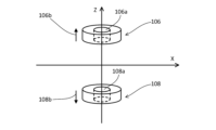
- the laser light pair LY includes a laser light LY1 that travels in the positive direction on the Y-axis and a laser light LY2 that travels in the negative direction on the Y-axis (that is, laser light LY2 that travels in the negative direction on the Y-axis). (laser light traveling in the opposite direction to the traveling direction of the light LY1).
- the magnets 106 and 108 are permanent magnets magnetized along the Z axis. That is, the magnets 106 and 108 are placed on the Z-axis so that the magnetization direction is parallel to the Z-axis direction. Specifically, the magnets 106 and 108 are installed such that the magnetization direction 106b of the magnet 106 and the magnetization direction 108b of the magnet 108 are opposite to each other with the center O of the intersection region 112 in between. . The distance between magnet 106 and center O is equal to the distance between magnet 108 and center O. Furthermore, the magnets 106 and 108 are placed close to the intersection area 112 so as not to block the laser beam pair LX, LY.
- the magnets 106 and 108 are installed on the optical path along which the laser light pair LZ, which is part of the three laser light pairs, travels, and the magnets 106 and 108 are installed on the optical path on which the laser light pair LZ, which is a part of the three laser light pairs, moves a part of the laser light pair LZ (that is, the laser lights LZ1 and LZ2). Partially mask.
- a laser beam group that is not masked by the magnets 106 and 108 that is, a laser beam group that includes the laser beam pair LX, the laser beam pair LY, and the laser beam that is not masked from the laser beam pair LZ
- a quadrupole magnetic field B formed by the magnets 106 and 108 an atom trapping space 102 is formed.
- a region 114 that is a non-atom trapping space is formed in a space where light is masked by the magnets 106 and 108.
- the relationship between the size (e.g. diameter) of the magnets 106, 108, the size (e.g. diameter) of the holes 106a, 108a, and the diameter of the magneto-optical trap laser light (laser light LZ1 etc.) is as shown below. becomes. Size of holes 106a, 108a ⁇ size of magnets 106, 108 ⁇ diameter of laser beam for magneto-optic trap
- a pair of laser beams LX, LY, and LZ is irradiated by the first irradiation device 104, and an intersection area 112 is formed. Further, a quadrupole magnetic field B is formed by the magnets 106 and 108. Further, the second irradiation device 116 irradiates the atom trapping space 102 with laser light 118 .
- the atoms that have moved outside the region 114 are irradiated with the laser light pair LZ, the atoms that have moved outside the region 114 are quadrupled by the laser light pairs LX, LY, LZ and the quadrupole magnetic field B. It is pulled back toward the center O of the polar magnetic field B.
- the wavelength of the laser light pair LX, LY, LZ is 689 nm.
- the width (outer diameter) of the magnets 106, 108 in the X direction and the Y direction is approximately 0.8 mm, and the width (inner diameter) of the holes 106a, 108a in the X direction and the Y direction is 0.27 mm.
- the distance between the magnet 106 and the magnet 108 is about 10 mm to 15 mm.
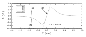
- FIG. 7 shows the calculated value of the magnetic field component on the Y-axis.
- the horizontal axis in FIG. 7 indicates the position on the Y-axis, and the vertical axis indicates the calculated value of the magnetic field.
- Reference numeral 122 indicates the calculated value of the X component of the magnetic field (BX) and the calculated value of the Z component of the magnetic field (BZ).
- Reference numeral 124 indicates the calculated value (BY) of the Y component of the magnetic field.
- a linear magnetic field gradient of +3.5 G/cm is created between -2 mm and +2 mm.
- a quadrupole magnetic field having a relatively small magnetic field gradient is formed.
- a magneto-optical trap using such a quadrupole magnetic field and a laser beam having a wavelength of 689 nm cools the atoms until their temperature reaches approximately ⁇ K.
- the atoms cooled to a temperature of approximately ⁇ K are supplied from the magneto-optical trap device 100 to a subsequent device.
- the mask member is an optical element such as a mirror in which a hole is formed
- the optical characteristics of the optical element may deteriorate due to the dirt.
- the magnets 106 and 108 in which the holes are formed function as masks, the problem of deterioration of the optical characteristics of the optical element does not occur.
- an optical lattice trap or the like is applied to the extremely low temperature atoms that have moved outside the intersection region 112.
- an optical grating light beam enters the vacuum chamber of the magneto-optic trap device 100 and is reflected by an optical resonator provided in the vacuum chamber, thereby creating a series of standing waves in the traveling direction of the optical grating light beam.
- An optical lattice potential is formed. The atomic population is trapped in the optical lattice potential.
- the light emitted as a result of the clock transition is received by the optical system device 14, and subjected to spectroscopic processing etc. by the control device 16 to determine the frequency.
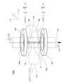
- the magneto-optical trap device 100A according to the second embodiment further includes a pair of auxiliary magnets in addition to the configuration of the magneto-optic trap device 100 according to the first embodiment.
- the pair of auxiliary magnets includes ring-shaped auxiliary magnets 160 and 162.
- a hole 160a is formed in the center of the auxiliary magnet 160, passing through the auxiliary magnet 160 in the magnetization direction.
- a hole 162a is formed in the center of the auxiliary magnet 162, passing through the auxiliary magnet 162 in the magnetization direction.
- the auxiliary magnets 160 and 162 are magnets magnetized along the Z axis. That is, the auxiliary magnets 160 and 162 are installed on the Z-axis so that the magnetization direction is parallel to the Z-axis direction.
- the direction of magnetization of the auxiliary magnets 160, 162 may be the same as the direction of magnetization of the magnets 106, 108, or the direction of magnetization of the auxiliary magnets 160, 162 may be in the radial direction.
- the magnets 106 and 108 may be soft magnets.
- the shape of the soft magnets is designed so that the lines of magnetic force coming out of the auxiliary magnets 160, 162 are bundled by the magnets 106, 108, which are soft magnets, and a quadrupole magnetic field is formed near the center O.
- anti-Helmholtz coils may be used to adjust the magnetic field distribution.
- the mask members 174 and 176 are made of paramagnetic material.
- the paramagnetic material has no optical effect and can mask part of the laser beam pair LZ. Since the mask members 174 and 176 are used only for masking, no problem occurs even if the surfaces of the mask members 174 and 176 on the intersection region 112 side become contaminated with atomic gas.
- mirrors 178 and 180 are only examples of optical elements that generate a pair of laser beams, and a pair of laser beams may be generated by using another optical element (for example, a beam splitter). The same applies to the first and second embodiments.
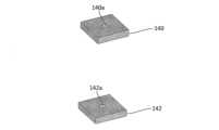
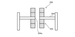
- FIGS. 17 and 18 are cross-sectional views showing ring-shaped magnets.
- a method can be considered in which a ring-shaped magnet is attached to a disc plate made of glass, sapphire, or the like that transmits light, and the disc plate is supported by a magneto-optical trap device.
- the magnet 200 is fixed to the disc plate 204 with an adhesive or indium ultrasonic solder that produces little outgassing.
- a metal pattern may be plated on glass, and the magnet 200 may be attached to the pattern using indium solder.
- an optical lattice clock was used as an example.
- the techniques of each embodiment described above can be applied to other than optical lattice clocks by those skilled in the art.
- it is applicable to atomic clocks other than optical lattice clocks, or atomic interferometers that are interferometers using atoms.
- a physics package for an atomic clock or a physics package for an atomic interferometer including the magneto-optical trap device 100, the magneto-optic trap device 100A, or the magneto-optic trap device 100B may be configured.
- the first to third embodiments are also applicable to various quantum information processing devices for atoms or ionized atoms.
- a quantum information processing device is a device that performs measurement, sensing, and information processing using the quantum states of atoms and light.In addition to atomic clocks and atomic interferometers, it also includes magnetic field meters, electric field meters, quantum computers, Examples include a quantum simulator and a quantum repeater.
- the physical package of the quantum information processing device can be made smaller or more portable, similar to the physical package of the optical lattice clock. Note that in such devices, the clock transition space is not a space for the purpose of clock measurement, but may simply be treated as a space where clock transition spectroscopy occurs.
Landscapes
- Physics & Mathematics (AREA)
- General Physics & Mathematics (AREA)
- Engineering & Computer Science (AREA)
- Spectroscopy & Molecular Physics (AREA)
- General Engineering & Computer Science (AREA)
- Theoretical Computer Science (AREA)
- Condensed Matter Physics & Semiconductors (AREA)
- Electromagnetism (AREA)
- Mathematical Analysis (AREA)
- Computing Systems (AREA)
- Computational Mathematics (AREA)
- Remote Sensing (AREA)
- Data Mining & Analysis (AREA)
- Evolutionary Computation (AREA)
- Radar, Positioning & Navigation (AREA)
- Mathematical Optimization (AREA)
- Pure & Applied Mathematics (AREA)
- Artificial Intelligence (AREA)
- Mathematical Physics (AREA)
- Software Systems (AREA)
- High Energy & Nuclear Physics (AREA)
- Plasma & Fusion (AREA)
- Optics & Photonics (AREA)
- Life Sciences & Earth Sciences (AREA)
- General Life Sciences & Earth Sciences (AREA)
- Geophysics (AREA)
- Lasers (AREA)
- Stabilization Of Oscillater, Synchronisation, Frequency Synthesizers (AREA)
Priority Applications (5)
| Application Number | Priority Date | Filing Date | Title |
|---|---|---|---|
| US18/874,386 US20250364151A1 (en) | 2022-06-14 | 2023-04-28 | Magnetic Optical Trap Device, Physics Package, Physics Package for Optical Lattice Clock, Physics Package for Atomic Clock, Physics Package for Atomic Interferometer, Physics Package for Quantum Information Processing Device, and Physics Package System |
| KR1020247041154A KR20250022045A (ko) | 2022-06-14 | 2023-04-28 | 자기 광학 트랩 장치, 물리 패키지, 광격자 시계용 물리 패키지, 원자 시계용 물리 패키지, 원자 간섭계용 물리 패키지, 양자 정보 처리 디바이스용 물리 패키지, 및 물리 패키지 시스템 |
| JP2024528363A JPWO2023243246A1 (https=) | 2022-06-14 | 2023-04-28 | |
| EP23823549.3A EP4542794A1 (en) | 2022-06-14 | 2023-04-28 | Magnetic optical trap device, physical package, physical package for optical lattice watch, physical package for atomic watch, physical package for atomic interferometer, physical package for quantom information processing device, and physical package system |
| CN202380047105.XA CN119384774A (zh) | 2022-06-14 | 2023-04-28 | 磁光阱装置、物理封装、光晶格钟用物理封装、原子钟用物理封装、原子干涉仪用物理封装、量子信息处理设备用物理封装以及物理封装系统 |
Applications Claiming Priority (2)
| Application Number | Priority Date | Filing Date | Title |
|---|---|---|---|
| JP2022-096079 | 2022-06-14 | ||
| JP2022096079 | 2022-06-14 |
Publications (1)
| Publication Number | Publication Date |
|---|---|
| WO2023243246A1 true WO2023243246A1 (ja) | 2023-12-21 |
Family
ID=89190989
Family Applications (1)
| Application Number | Title | Priority Date | Filing Date |
|---|---|---|---|
| PCT/JP2023/016938 Ceased WO2023243246A1 (ja) | 2022-06-14 | 2023-04-28 | 磁気光学トラップ装置、物理パッケージ、光格子時計用物理パッケージ、原子時計用物理パッケージ、原子干渉計用物理パッケージ、量子情報処理デバイス用物理パッケージ、及び、物理パッケージシステム |
Country Status (6)
| Country | Link |
|---|---|
| US (1) | US20250364151A1 (https=) |
| EP (1) | EP4542794A1 (https=) |
| JP (1) | JPWO2023243246A1 (https=) |
| KR (1) | KR20250022045A (https=) |
| CN (1) | CN119384774A (https=) |
| WO (1) | WO2023243246A1 (https=) |
Cited By (1)
| Publication number | Priority date | Publication date | Assignee | Title |
|---|---|---|---|---|
| WO2025142640A1 (ja) * | 2023-12-28 | 2025-07-03 | 国立研究開発法人理化学研究所 | 原子トラップ装置、原子冷却装置、分光装置、光格子時計、量子コンピュータ、コイル、原子トラップ方法、原子冷却方法および分光方法 |
Citations (12)
| Publication number | Priority date | Publication date | Assignee | Title |
|---|---|---|---|---|
| US5274232A (en) | 1992-04-14 | 1993-12-28 | Board Of Trustees, Leland Stanford Jr. University | Method and apparatus for manipulating atoms, ions or molecules and for measuring physical quantities using stimulated raman transitions |
| US6303928B1 (en) * | 1998-12-21 | 2001-10-16 | The Aerospace Corporation | Continuous cold atom beam atomic system |
| JP2004058225A (ja) * | 2002-07-30 | 2004-02-26 | Inst Of Physical & Chemical Res | クラスタおよび異元素内包クラスタの生成方法および生成装置 |
| JP6206973B2 (ja) | 2012-08-17 | 2017-10-04 | 国立研究開発法人理化学研究所 | 光格子時計、時計装置、およびレーザー光源 |
| US10371763B2 (en) | 2015-07-17 | 2019-08-06 | Honeywell International Inc. | Systems and methods for low power magnetic field generation for atomic sensors using electro-permanent magnets |
| JP6635608B2 (ja) | 2015-01-30 | 2020-01-29 | 国立研究開発法人理化学研究所 | 実効的魔法周波数の光格子時計およびその動作方法 |
| CN210016681U (zh) * | 2019-02-26 | 2020-02-04 | 北京大学 | 一种冷铯原子束源 |
| JP2020020636A (ja) * | 2018-07-31 | 2020-02-06 | 日本航空電子工業株式会社 | 冷却原子線生成方法、冷却原子線生成装置、原子干渉計 |
| JP2021163883A (ja) * | 2020-03-31 | 2021-10-11 | 日本電子株式会社 | 物理パッケージ、光格子時計用物理パッケージ、原子時計用物理パッケージ、原子干渉計用物理パッケージ、及び、量子情報処理デバイス用物理パッケージ |
| JP2022014486A (ja) | 2020-07-07 | 2022-01-20 | 日華化学株式会社 | 毛髪用化粧料 |
| JP7189588B2 (ja) | 2018-01-19 | 2022-12-14 | 国立研究開発法人理化学研究所 | 輻射シールドおよびそれを利用する光格子時計 |
| JP2023021719A (ja) * | 2021-08-02 | 2023-02-14 | 日本電気株式会社 | 量子干渉装置、原子発振器及び制御方法 |
Family Cites Families (1)
| Publication number | Priority date | Publication date | Assignee | Title |
|---|---|---|---|---|
| JPS626973Y2 (https=) | 1981-05-15 | 1987-02-18 |
-
2023
- 2023-04-28 JP JP2024528363A patent/JPWO2023243246A1/ja active Pending
- 2023-04-28 WO PCT/JP2023/016938 patent/WO2023243246A1/ja not_active Ceased
- 2023-04-28 EP EP23823549.3A patent/EP4542794A1/en active Pending
- 2023-04-28 US US18/874,386 patent/US20250364151A1/en active Pending
- 2023-04-28 KR KR1020247041154A patent/KR20250022045A/ko active Pending
- 2023-04-28 CN CN202380047105.XA patent/CN119384774A/zh active Pending
Patent Citations (12)
| Publication number | Priority date | Publication date | Assignee | Title |
|---|---|---|---|---|
| US5274232A (en) | 1992-04-14 | 1993-12-28 | Board Of Trustees, Leland Stanford Jr. University | Method and apparatus for manipulating atoms, ions or molecules and for measuring physical quantities using stimulated raman transitions |
| US6303928B1 (en) * | 1998-12-21 | 2001-10-16 | The Aerospace Corporation | Continuous cold atom beam atomic system |
| JP2004058225A (ja) * | 2002-07-30 | 2004-02-26 | Inst Of Physical & Chemical Res | クラスタおよび異元素内包クラスタの生成方法および生成装置 |
| JP6206973B2 (ja) | 2012-08-17 | 2017-10-04 | 国立研究開発法人理化学研究所 | 光格子時計、時計装置、およびレーザー光源 |
| JP6635608B2 (ja) | 2015-01-30 | 2020-01-29 | 国立研究開発法人理化学研究所 | 実効的魔法周波数の光格子時計およびその動作方法 |
| US10371763B2 (en) | 2015-07-17 | 2019-08-06 | Honeywell International Inc. | Systems and methods for low power magnetic field generation for atomic sensors using electro-permanent magnets |
| JP7189588B2 (ja) | 2018-01-19 | 2022-12-14 | 国立研究開発法人理化学研究所 | 輻射シールドおよびそれを利用する光格子時計 |
| JP2020020636A (ja) * | 2018-07-31 | 2020-02-06 | 日本航空電子工業株式会社 | 冷却原子線生成方法、冷却原子線生成装置、原子干渉計 |
| CN210016681U (zh) * | 2019-02-26 | 2020-02-04 | 北京大学 | 一种冷铯原子束源 |
| JP2021163883A (ja) * | 2020-03-31 | 2021-10-11 | 日本電子株式会社 | 物理パッケージ、光格子時計用物理パッケージ、原子時計用物理パッケージ、原子干渉計用物理パッケージ、及び、量子情報処理デバイス用物理パッケージ |
| JP2022014486A (ja) | 2020-07-07 | 2022-01-20 | 日華化学株式会社 | 毛髪用化粧料 |
| JP2023021719A (ja) * | 2021-08-02 | 2023-02-14 | 日本電気株式会社 | 量子干渉装置、原子発振器及び制御方法 |
Non-Patent Citations (3)
| Title |
|---|
| M. GREINER, PHYS. REV. A, vol. 63, 2001, pages 031401 |
| R17 F. SHIMIZU, PHYS. REV. A, vol. 46, 1992 |
| Z. T. LIU, PHYS. REV. LETT, vol. 77, 1996, pages 3331 |
Cited By (1)
| Publication number | Priority date | Publication date | Assignee | Title |
|---|---|---|---|---|
| WO2025142640A1 (ja) * | 2023-12-28 | 2025-07-03 | 国立研究開発法人理化学研究所 | 原子トラップ装置、原子冷却装置、分光装置、光格子時計、量子コンピュータ、コイル、原子トラップ方法、原子冷却方法および分光方法 |
Also Published As
| Publication number | Publication date |
|---|---|
| EP4542794A1 (en) | 2025-04-23 |
| US20250364151A1 (en) | 2025-11-27 |
| JPWO2023243246A1 (https=) | 2023-12-21 |
| CN119384774A (zh) | 2025-01-28 |
| KR20250022045A (ko) | 2025-02-14 |
Similar Documents
| Publication | Publication Date | Title |
|---|---|---|
| Chkhalo et al. | Source for extreme ultraviolet lithography based on plasma sustained by millimeter-wave gyrotron radiation | |
| US8288712B2 (en) | Guided coherent atom source and atomic interferometer | |
| Sugarbaker | Atom interferometry in a 10 m fountain | |
| Fujimoto et al. | Laser-produced plasma-based extreme-ultraviolet light source technology for high-volume manufacturing extreme-ultraviolet lithography | |
| WO2023243246A1 (ja) | 磁気光学トラップ装置、物理パッケージ、光格子時計用物理パッケージ、原子時計用物理パッケージ、原子干渉計用物理パッケージ、量子情報処理デバイス用物理パッケージ、及び、物理パッケージシステム | |
| WO2022181408A1 (ja) | 原子の電子状態スプリッター、原子干渉計、原子遷移周波数測定装置、原子発振器、光格子時計、量子コンピュータおよび原子の電子状態重ね合わせ状態の生成方法 | |
| TWI706695B (zh) | 波盪器、磁場感測器、波盪器模組、自由電子雷射、微影系統、及判定波盪器模組之磁場強度之方法 | |
| Dulat et al. | Coherent control of relativistic electron dynamics in plasma nanophotonics | |
| KR20250024944A (ko) | 냉각 원자 생성 장치, 냉각 원자 생성 방법, 물리 패키지, 광격자 시계용 물리 패키지, 원자 시계용 물리 패키지, 원자 간섭계용 물리 패키지, 양자 정보 처리 디바이스용 물리 패키지, 및 물리 패키지 시스템 | |
| JP6764876B2 (ja) | 測定装置及び方法 | |
| WO2022045146A1 (ja) | 量子シミュレータおよび量子シミュレーション方法 | |
| WO2023149159A1 (ja) | 磁気光学トラップ装置、物理パッケージ、光格子時計用物理パッケージ、原子時計用物理パッケージ、原子干渉計用物理パッケージ、量子情報処理デバイス用物理パッケージ、及び、物理パッケージシステム | |
| Hung | In situ probing of two-dimensional quantum gases | |
| JP7773733B2 (ja) | 低速原子ビーム生成装置、物理パッケージ、光格子時計用物理パッケージ、原子時計用物理パッケージ、原子干渉計用物理パッケージ、量子情報処理デバイス用物理パッケージ、及び、物理パッケージシステム | |
| Hagemann | A Setup for High-Resolution Imaging of Ultracold Lithium Atoms | |
| Tell | A prototype apparatus for very long baseline atom interferometry | |
| Xu et al. | A proposal of multipulse-driven split-ring resonator for femtosecond resolution bunch length measurement | |
| Castro et al. | Ion acceleration in non-equilibrium plasmas driven by fast drifting electron | |
| Sakabe et al. | Generation of Intense Short Electron Pulses Using High‐Intensity Lasers | |
| Marsegan | Positron interferometry: towards the study of microwave influence | |
| JP2022040884A (ja) | 量子シミュレータおよび量子シミュレーション方法 | |
| Li et al. | Ultrafast dynamics of magnetic vortices and pulse collapse in a laser-under dense plasma interaction | |
| Vogel | Optical guiding of high intensity laser pulses in plasma channel: Interferometrical investigations | |
| Sinclair | Bose-Einstein condensation in microtraps on videotape | |
| Zhang | One-dimensional fermi gases with rapid control of interactions: Toward the observation of Dicke states and exotic superfluid pairing |
Legal Events
| Date | Code | Title | Description |
|---|---|---|---|
| 121 | Ep: the epo has been informed by wipo that ep was designated in this application |
Ref document number: 23823549 Country of ref document: EP Kind code of ref document: A1 |
|
| ENP | Entry into the national phase |
Ref document number: 2024528363 Country of ref document: JP Kind code of ref document: A |
|
| WWE | Wipo information: entry into national phase |
Ref document number: 18874386 Country of ref document: US |
|
| WWE | Wipo information: entry into national phase |
Ref document number: 202380047105.X Country of ref document: CN |
|
| WWE | Wipo information: entry into national phase |
Ref document number: 2023823549 Country of ref document: EP Ref document number: 2024139517 Country of ref document: RU |
|
| NENP | Non-entry into the national phase |
Ref country code: DE |
|
| ENP | Entry into the national phase |
Ref document number: 2023823549 Country of ref document: EP Effective date: 20250114 |
|
| WWP | Wipo information: published in national office |
Ref document number: 202380047105.X Country of ref document: CN |
|
| WWP | Wipo information: published in national office |
Ref document number: 1020247041154 Country of ref document: KR |
|
| WWP | Wipo information: published in national office |
Ref document number: 2024139517 Country of ref document: RU |
|
| WWP | Wipo information: published in national office |
Ref document number: 2023823549 Country of ref document: EP |
|
| WWP | Wipo information: published in national office |
Ref document number: 18874386 Country of ref document: US |