WO2023228705A1 - 通信装置 - Google Patents
通信装置 Download PDFInfo
- Publication number
- WO2023228705A1 WO2023228705A1 PCT/JP2023/017236 JP2023017236W WO2023228705A1 WO 2023228705 A1 WO2023228705 A1 WO 2023228705A1 JP 2023017236 W JP2023017236 W JP 2023017236W WO 2023228705 A1 WO2023228705 A1 WO 2023228705A1
- Authority
- WO
- WIPO (PCT)
- Prior art keywords
- antenna
- antenna element
- communication device
- inductor
- capacitor
- Prior art date
- Legal status (The legal status is an assumption and is not a legal conclusion. Google has not performed a legal analysis and makes no representation as to the accuracy of the status listed.)
- Ceased
Links
Images


Classifications
-
- H—ELECTRICITY
- H01—ELECTRIC ELEMENTS
- H01Q—ANTENNAS, i.e. RADIO AERIALS
- H01Q21/00—Antenna arrays or systems
- H01Q21/24—Combinations of antenna units polarised in different directions for transmitting or receiving circularly and elliptically polarised waves or waves linearly polarised in any direction
-
- H—ELECTRICITY
- H01—ELECTRIC ELEMENTS
- H01Q—ANTENNAS, i.e. RADIO AERIALS
- H01Q1/00—Details of, or arrangements associated with, antennas
- H01Q1/04—Adaptation for subterranean or subaqueous use
-
- H—ELECTRICITY
- H01—ELECTRIC ELEMENTS
- H01Q—ANTENNAS, i.e. RADIO AERIALS
- H01Q9/00—Electrically-short antennas having dimensions not more than twice the operating wavelength and consisting of conductive active radiating elements
- H01Q9/04—Resonant antennas
- H01Q9/0407—Substantially flat resonant element parallel to ground plane, e.g. patch antenna
- H01Q9/0428—Substantially flat resonant element parallel to ground plane, e.g. patch antenna radiating a circular polarised wave
-
- H—ELECTRICITY
- H01—ELECTRIC ELEMENTS
- H01Q—ANTENNAS, i.e. RADIO AERIALS
- H01Q9/00—Electrically-short antennas having dimensions not more than twice the operating wavelength and consisting of conductive active radiating elements
- H01Q9/04—Resonant antennas
- H01Q9/30—Resonant antennas with feed to end of elongated active element, e.g. unipole
Definitions
- the present technology relates to a communication device, for example, to a communication device suitable for use in communication in liquid.
- Patent Document 1 proposes a communication device that communicates with a communication device that is separated underwater.
- the present technology was developed in view of this situation, and enables stable communication even with an electrically small size antenna.
- a first communication device is a circularly polarized wave composed of a first antenna element and a second antenna element arranged orthogonally to the first antenna element.
- the phase shifter includes an antenna, a capacitor connected to the first antenna element, and an inductor connected to the second antenna element, R is a resistance, j is an imaginary unit,
- R is a resistance
- j is an imaginary unit
- the impedance of the antenna is expressed as R+jX
- a second communication device includes a circularly polarized antenna including a first antenna element and a second antenna element having orthogonal linearly polarized waves, and a circularly polarized antenna that is connected to the first antenna element.
- a phase shifter composed of a capacitor connected to the second antenna element and an inductor connected to the second antenna element, R is a resistance, j is an imaginary unit, X is a reactance, and the center frequency of the antenna is f,
- the impedance of the antenna is expressed as R+jX
- a circularly polarized wave including a first antenna element and a second antenna element arranged orthogonally to the first antenna element.
- a phase shifter is provided, which includes an antenna, a capacitor connected to the first antenna element, and an inductor connected to the second antenna element.
- R resistance
- j an imaginary unit
- X reactance
- the center frequency of the antenna is f
- capacitance is C
- inductance L
- the impedance of the antenna is expressed as R+jX
- the capacitance of the capacitor 1/ ⁇ f(R+X) ⁇
- a second communication device includes a circularly polarized antenna including a first antenna element and a second antenna element having orthogonal linearly polarized waves, and a circularly polarized antenna connected to the first antenna element. and a phase shifter including a capacitor connected to the second antenna element and an inductor connected to the second antenna element.
- the communication device may be an independent device or an internal block forming one device.
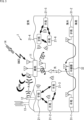
- FIG. 1 is a diagram showing the configuration of an embodiment of a communication system to which the present technology is applied.
- FIG. 3 is a diagram showing the configuration of another embodiment of a communication system to which the present technology is applied.
- FIG. 3 is a diagram showing the configuration of another embodiment of a communication system to which the present technology is applied.
- FIG. 3 is a diagram illustrating a configuration example of a master station.
- FIG. 3 is a diagram showing a configuration example of an antenna and a phase shifter.
- FIG. 3 is a diagram for explaining conditions regarding the configuration of a phase shifter. It is a figure showing the example of composition of a phase shifter. It is a figure showing the example of composition of a phase shifter.
- FIG. 3 is a diagram illustrating a configuration example of a phase shifter to which a balun is added.
- FIG. 3 is a diagram illustrating a configuration example of a phase shifter to which a balun is added.
- FIG. 2 is a diagram illustrating a configuration example of a phase shifter to which a matching circuit is added. It is a figure which shows the other example of a structure of a phase shifter. It is a figure which shows the other example of a structure of a phase shifter. It is a figure which shows the other example of a structure of a phase shifter. It is a figure which shows the other example of a structure of a phase shifter. It is a figure which shows the other example of a structure of a phase shifter.
- FIG. 3 is a diagram for explaining the shape of an antenna.
- FIG. 3 is a diagram for explaining the shape of an antenna.
- FIG. 3 is a diagram for explaining the shape of an antenna. It is a figure showing an example of composition of an antenna. It is a figure showing an example of composition of an antenna. It is a figure showing an example of composition of an antenna. It is a figure showing an example of composition of an antenna.
- FIG. 1 is a diagram showing the configuration of an embodiment of a communication system 1 to which the present technology is applied.
- the communication system 1 shown in FIG. include.
- the slave stations 21-1 to 21-6 will be simply referred to as slave stations 21 when there is no need to distinguish them individually. The same applies to other parts.
- the master station 11 and the communication station 12 perform communication using local 5G, for example.
- the master station 11 and the communication station 13 communicate using, for example, LPWA (Low Power Wide Area).
- the master station 11 is configured to be able to acquire position information from the satellite 14 using, for example, GNSS (Global Navigation Satellite System).
- GNSS Global Navigation Satellite System
- the master station 11 also communicates with the slave station 21.
- the portion of the master station 11 that communicates with the communication station 12, the communication station 13, and the satellite 14 described above is located in the air, and the portion that communicates with the slave station 21 is located in the seawater.
- the slave station 21 is located in seawater.
- the communication system 1 will be described here taking as an example the environment in which it is installed in the ocean, it can also be installed in environments such as lakes, ponds, rivers, and aquariums.
- the present technology described below can be applied to a device installed in a medium (lossy medium) other than lossless air.
- Lossy media include not only seawater and brackish lakes described above, but also the inside of the human body.
- one of the master stations 11 is located in the air (gas) and the other is located in seawater (liquid), but one may be located in the seabed (solid) or in vacuum.
- the master station 11 may also be located at a remote location.
- the configuration of the communication system 1 shown in FIG. 1 is an example and is not a limitation.
- the master station 11 communicates with the communication station 12, the communication station 13, and the satellite 14, but it may also have the function of communicating with other than these. However, instead of having the function of communicating with all of them, it may be configured to be able to communicate with one or two of them.
- the master station 11 may have a configuration in which it only has the function of communicating with the slave station 21, in other words, it does not have the function of communicating with the communication station 12, the communication station 13, or the satellite 14.
- the slave stations 21-1 to 21-6 each communicate with the master station 11.
- a so-called ad hoc network may be configured in which slave stations 21 communicate with each other.
- the slave station 21 includes, for example, a sensor that senses the underwater environment, and transmits the sensed data to the master station 11.
- the slave station 21 may be configured to have only a transmitting function for transmitting data to the master station 11, or may have a transmitting function and a receiving function for transmitting and receiving data to and from the master station 11 and other slave stations 21. It can also be configured.
- the slave station 21 is installed at a depth from the sea surface within a range of, for example, 0 to 10 m.
- the slave stations 31-1 and 31-2 each communicate with the repeater 32.
- the slave station 31 includes, for example, a sensor that senses the underwater environment, and transmits the sensed data to the repeater 32.
- the slave station 31 may be configured to have only a transmitting function for transmitting data to the repeater 32, or may have a transmitting function and a receiving function for transmitting and receiving data to and from the repeater 32 and other slave stations 31. It can also be configured.
- the slave station 31 is installed on the ocean floor (near the ocean floor).
- the antenna that is installed in seawater (liquid) and used for communication with the slave station 21 and repeater 32 installed in the seawater is a circularly polarized antenna.
- the antennas of the slave station 21 and the slave station 31 may be circularly polarized antennas or linearly polarized antennas.
- the antenna of the repeater 32 is a circularly polarized antenna, and in the example shown in FIG. 1, it is used when communicating with the slave station 31 and when communicating with the master station 11.
- the relay 32 and the master station 11 may be configured to communicate by wire.
- optical communication may be used between the repeater 32 and the master station 11.
- the slave station 21 and the slave station 31 are grounded in the sea or on the seabed, the positional relationship with the master station 11 and the repeater 32 may deviate from the positional relationship suitable for communication due to the influence of waves.
- a circularly polarized antenna as the antenna on the receiving side that receives data from the master station 11 and the repeater 32, in other words, the slave station 21 and the slave station 31, it is possible to prevent Even in this case, relatively good communication can be maintained.
- the signal from the slave station 21 installed underwater is propagated to the master station 11 through a direct wave that travels in a straight line between the antenna of the slave station 21 and the antenna of the master station 11, and a direct wave that propagates in a straight line between the antenna of the slave station 21 and the antenna of the master station 11.
- the lateral wave becomes dominant and is received by the master station 11. Since lateral waves propagate farther than direct waves, the greater the distance between slave station 21 and master station 11, the more lateral waves become dominant. This phenomenon occurs when the antenna is not far from the sea surface.
- the signal from the slave station 31 installed on the ocean floor is propagated to the repeater 32 through a direct wave that travels in a straight line between the antenna of the slave station 31 and the antenna of the repeater 32, and a direct wave that propagates in a straight line between the antenna of the slave station 31 and the antenna of the repeater 32.
- the signal propagated from the slave station 31 into the seawater has a large attenuation, but the signal propagated along the seabed from the slave station 31 has a small attenuation. is received. Signals propagating along the ocean floor allow networks to be spread over larger areas. Power consumption of the slave station 31 can be reduced. When a mesh network is configured by the slave stations 31, the number of terminals required for the mesh network can be reduced.
- FIG. 4 is a diagram showing an example of the configuration of the master station 11.
- the master station 11 shown in FIG. 4 includes a signal processing section 101, a high frequency processing section 102, and an antenna 103.
- Antenna 103 of master station 11 is installed in seawater (liquid) and is used for communication with slave station 21, repeater 32, and other master stations 11 installed in seawater.
- Antenna 103 is a circularly polarized antenna.
- the signal from the slave station 21 is received by the antenna 103 of the master station 11 and supplied to the high frequency processing section 102.
- the high frequency processing unit 102 is configured to process, for example, a received signal and a transmitted signal.
- the operating frequency fw of the high frequency processing section 102 is set to, for example, 1 MHz or less.
- the signal processed by the high frequency processing section 102 is supplied to the signal processing section 101.
- the signal processing unit 101 performs processing such as temporarily storing a signal processed by the high frequency processing unit 102 or processing a received signal and transmitting the processed signal.
- the configuration of the master station 11 shown in FIG. 4 can also be applied to the configuration of the repeater 32.
- the antenna 103 has the function of receiving signals from the slave station 31 and the function of transmitting signals to the master station 11 or other repeaters 32.
- the high frequency processing section 102 and the signal processing section 101 have a function of amplifying a received signal and transmitting it.
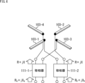
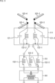
- FIG. 5 is a diagram showing a configuration example of the antenna 103 and the phase shifter 111 included in the high frequency processing section 102.
- the antenna 103 and phase shifter 111 included in the master station 11 will be explained as an example, but it is also applicable to any of the slave stations 21, 31, and repeaters 32. .
- the antenna 103 is a circularly polarized antenna, and in the example shown in FIG. 5, it is composed of antenna elements 103-1 to 103-4.
- a pair of antenna elements 103-1 and 103-2 are arranged on a straight line and constitute a dipole antenna.
- the pair of antenna elements 103-3 and 103-4 are arranged on a straight line and constitute a dipole antenna.
- a dipole antenna consisting of antenna element 103-1 and antenna element 103-2 and a dipole antenna consisting of antenna element 103-3 and antenna element 103-4 are arranged so as to intersect at 90 degrees.
- the antenna 103 is a cross dipole antenna composed of antenna elements 103-1 to 103-4, and is a circularly polarized antenna.
- the antenna 103 shown in FIG. 5 uses two sets of balanced linearly polarized antennas, and the antenna elements (radiating elements) constituting the orthogonally polarized antennas are arranged so as to be orthogonal to each other, resulting in circular polarization.
- An antenna that can transmit and receive wave signals.
- Antenna element 103-1 and antenna element 103-2 are connected to phase shifter 111-2.
- Antenna element 103-3 and antenna element 103-4 are connected to phase shifter 111-1.
- the master station 11 including the phase shifter 111 having such a configuration is installed in a medium having high conductivity such as seawater.
- a medium having high conductivity electromagnetic waves are attenuated significantly, and when communication is performed over a distance of several meters, communication is generally performed using a frequency below the MHz band.
- the length of one wavelength is on the order of several meters, and for example, the size of a half-wavelength antenna may be considerably large compared to the communication device.
- the length of one wavelength is on the order of several meters, and if the antenna 103 is a resonant antenna such as a half-wavelength dipole antenna, the size of the antenna 103 may become large.
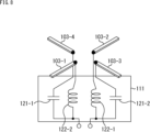
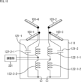
- FIG. 6 is a diagram in which the impedance in the phase shifter 111 is added to the phase shifter 111 and the antenna 103 shown in FIG. 5.
- the impedance of the electrically small antenna (antenna 103) shown in FIG. 6 is R+jX.
- R in impedance R+jX is the real part of impedance and represents resistance.
- jX of R+jX is the imaginary part of impedance, j represents an imaginary unit, and X represents reactance.
- Impedance R+jX is the impedance of one pair of antenna elements 103, for example, antenna element 103-1 and antenna element 103-2, when viewed from the phase shifter 111 side.
- the impedance of phase shifter 111-1 when viewed from the power feeding side is Ra+jXa
- the impedance when antenna 103 is viewed from phase shifter 111-1 is R+jX.
- the impedance to phase shifter 111-2 is Rb+jXb
- the impedance from phase shifter 111-1 is R+jX.
- each orthogonal antenna In order to obtain circularly polarized waves by orthogonally arranging a dipole antenna consisting of antenna elements 103-1 and 103-2 and a dipole antenna consisting of antenna elements 103-3 and 103-4, the impedance of each orthogonal antenna must be adjusted.
- the phase shifter 111 may be connected to each antenna 103 so that the phase difference between the two antennas is 90 degrees.
- the condition for the phase difference to be 90 degrees is expressed by the following equation (1).
- Ra ⁇ Rb+Xa ⁇ Xb 0 (1)
- the phase shifter 111-1 has a capacitance C shown by the following equation (5)
- the phase shifter 111-2 has a capacitance C shown by the following equation (6).
- a configuration having an inductance L may be used.
- f represents the center frequency of the frequency to be transmitted or received (desired frequency).
- the phase shifter 111-1 includes a capacitor 121-1 and a capacitor 121-2 having a capacitance C calculated by equation (5).
- the phase shifter 111-2 includes an inductor 122-1 and an inductor 122-2 having an inductance L calculated by equation (6).
- Capacitor 121-1 in phase shifter 111-1 is provided between a high frequency power source (not shown) and antenna element 103-4, and capacitor 121-2 is provided between high frequency power source and antenna element 103-3. It is set in.
- Inductor 122-1 in phase shifter 111-2 is provided between the high frequency power source and antenna element 103-2, and inductor 122-2 is provided between the high frequency power source and antenna element 103-1. There is.
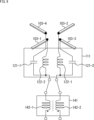
- phase shifter 111-1 and phase shifter 111-2 in FIG. 7 are collectively referred to as phase shifter 111.
- the phase shifter 111 includes an inductor 122-1 and an inductor 122-2 connected to the antenna element 103-1 and the antenna element 103-2, respectively. Further, phase shifter 111 includes a capacitor 121-1 and a capacitor 121-2 connected to antenna element 103-3 and antenna element 103-4, respectively.
- Capacitor 121-1 of phase shifter 111 is provided between a high frequency power source (not shown) and antenna element 103-4, and inductor 122-2 is provided between the high frequency power source and antenna element 103-1. ing. On the power supply side, capacitor 121-1 and inductor 122-2 are short-circuited.
- Capacitor 121-2 of phase shifter 111 is provided between the high frequency power source and antenna element 103-3, and inductor 122-1 is provided between the high frequency power source and antenna element 103-2. On the power supply side, capacitor 121-2 and inductor 122-1 are short-circuited.
- phase shifter 111 By configuring the phase shifter 111 in this way, it is possible to configure an ideal circularly polarized antenna with an axial ratio of 1 at the frequency f. Further, the phase shifter 111 that can obtain such an effect can be realized using four lumped constants. Therefore, the master station 11, the slave stations 21 and 31, and the repeater 32 including the phase shifter 111 and the antenna 103 can be downsized and manufactured at low cost.
- FIG. 9 is a diagram showing another configuration example of the phase shifter 111.
- the phase shifter 111 shown in FIG. 9 differs from the phase shifter 111 shown in FIG. 8 in that a balun 141 is added, and is similar in other respects. Inserting a balun can reduce noise and stabilize characteristics.
- the balun 141 illustrated in FIG. 9 is a float balun and includes a transformer 142-1 and a transformer 142-2. These two transformers are constructed by, for example, bifilar winding around the glasses core so that the polarities are the same.
- FIG. 10 is an example of the configuration of the phase shifter 111 to which a balun is added.
- the added balun 151 is a balun called a forced balun.
- the balun 151 is composed of transformers 151-1 to 151-3.
- the balun 151 is, for example, a toroidal core with three wires wound in a trifilar manner and wired so as to have an impedance conversion ratio of 1:1, and forcibly converts between balanced and unbalanced states.
- a matching circuit 161 may be added to the balun 151.
- the matching circuit 161 includes a transformer composed of a primary coil and a secondary coil, and transmits power by using mutual induction between the primary coil and the secondary coil. , impedance matching is performed by converting the voltage and impedance depending on the winding ratio of the two coils.
- FIG. 11 shows a configuration in which a matching circuit 161 is added to the balun 151
- a configuration in which the matching circuit 161 is added to the balun 141 may also be used.
- FIG. 12 is a diagram showing the configuration of another phase shifter 111.
- the phase shifter 111 shown in FIG. 12 has the same configuration as the phase shifter 111 shown in FIG. They are different in that they are composed of , and are similar in other respects.
- the capacitors 121-1' and 121-1' can be capacitors whose capacitance is variable by external control, such as a varicap.
- the phase shifter 111 is included in the master station 11, for example, and the master station 11 is assumed to be affected by the surrounding environment.
- the impedance of the antenna 103 may change due to the influence of the surrounding environment on the master station 11.
- the capacitance of the capacitor 121 is made variable so that it can follow such changes in the impedance of the antenna 103 and return (adjust) it to an appropriate impedance.
- the inductor 122 may also be variable. Further, both the capacitor 121 and the inductor 122 may be variable. At least one of the capacitor 121 and the inductor 122 can be configured to be variable.
- the phase shifter 111 may be provided with an adjustment section that adjusts the variable capacitor 121 and/or inductor 122 in accordance with changes in impedance.
- a configuration may also be adopted in which the balun 141 (FIG. 9) or the balun 151 (FIG. 10) is connected to the phase shifter 111 shown in FIG. 12. Furthermore, a configuration may be adopted in which a balun 151 (141) and a matching circuit 161 are connected to the phase shifter 111 shown in FIG.
- FIG. 13 is a diagram showing the configuration of another phase shifter 111.
- the phase shifter 111 shown in FIG. 13 is similar to the phase shifter 111 shown in FIG. 8 except that a resistor 201 is added.
- ESR equivalent series resistance
- a compensation circuit may be included so that the ideal capacitance C and inductance L calculated using equations (5) and (6) are achieved.
- a resistor 201 having a resistance value corresponding to the equivalent series resistance is provided on the capacitor 121 side so that the equivalent series resistance of the inductor 122 does not upset the impedance balance.
- a resistor 201-1 is connected in series to the capacitor 121-1 of the phase shifter 111, and a resistor 201-2 is connected in series to the capacitor 121-2.
- the phase shifter 111 shown in FIG. 14 shows a configuration example in which an inductor 122 is provided in parallel as a compensation circuit.
- an inductor 122-1-1 and an inductor 122-1-2 are connected in parallel, one end is connected to the antenna element 103-2, and the other end is connected to a power source (not shown). It is connected.
- an inductor 122-2-1 and an inductor 122-2-2 are connected in parallel, one end is connected to the antenna element 103-1, and the other end is connected to a power source (not shown). It is connected to the.
- the inductors 122 By arranging the inductors 122 in parallel, a configuration can be achieved in which the influence of the equivalent series resistance of the inductors 122 can be reduced. Furthermore, if the inductance L shown in equation (6) cannot be obtained with one inductor 122, for example, there is no element in the E12 series or E24 series that corresponds to the inductance L calculated by equation (6). In this case, by using a plurality of inductors 122, it is possible to configure the inductance L to be calculated by equation (6).
- the inductors 122 may be connected in series, as shown in FIG. 15, instead of being connected in parallel.
- the phase shifter 111 shown in FIG. 15 shows a configuration example in which an inductor 122 is provided in series as a compensation circuit, and an adjustment section 221 is added.
- an inductor 122-1-1 and an inductor 122-1-2 are connected in series, one end is connected to the antenna element 103-2, and the other end is connected to a power source (not shown). It is connected.
- an inductor 122-2-1 and an inductor 122-2-2 are connected in series, one end is connected to the antenna element 103-1, and the other end is connected to a power source (not shown). It is connected to the.
- An adjustment section 221 is provided between the inductors 122-1-1 and 122-1-2 and between the inductors 122-2-1 and 122-2-2, which are connected in series. This adjustment section 221 adjusts the inductance L of the inductor 122-1 composed of the inductor 122-1-1 and the inductor 122-1-2, and the inductance L of the inductor 122-1 composed of the inductor 122-2-1 and the inductor 122-2-2. The inductance L of 122-2 is adjusted.
- a configuration may also be adopted in which the balun 141 (FIG. 9) or the balun 151 (FIG. 10) is connected to the phase shifter 111 shown in FIGS. 12 to 15. Furthermore, a configuration may be adopted in which a balun 151 (141) and a matching circuit 161 are connected to the phase shifter 111 shown in FIGS. 12 to 15.
- the structure is such that circuits such as the phase shifter 111 are protected with resin such as silicone for waterproofing.
- parasitic impedance may occur with materials such as silicon.
- the configuration may include a compensation circuit that takes into consideration the occurrence of such parasitic impedance that occurs during operation.
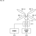
- FIG. 16 is a diagram showing an example of a configuration in which the antenna is configured with a propeller antenna 301.
- the antenna shown in FIG. 16 is composed of antenna elements 301-1 to 301-4, and is configured in a propeller type.
- the propeller-shaped antenna element 301 has a shape that rotates by wave power or tidal power.
- each antenna element 301 is processed into a shape that easily receives wave force, and the antenna 301 is processed into a shape that is easily rotated by wave force.
- the antenna element 301 constitutes a cross dipole antenna like the above-mentioned antenna element 103 (FIG. 8).
- Antenna element 301 is connected to phase shifter 111.
- the phase shifter 111 has a configuration to which any of the phase shifters 111 described with reference to FIGS. 8 to 15 is applied.
- the output from the phase shifter 111 is supplied to a movable contact section 311 using a slip ring or the like.
- a terminal connected to the antenna element 301 is provided on the antenna element 301 side of the movable contact portion 311, and the terminal is configured to rotate in accordance with the rotation of the antenna element 301.
- the terminal provided in contact with the rotating terminal is a fixed terminal and is connected to the transmitting/receiving circuit 312.
- the transmitting/receiving circuit 312 processes the signal received by the antenna element 301 that is supplied via the movable contact portion 311. Further, the transmitting/receiving circuit 312 generates a signal to be transmitted by the antenna element 301 and supplies it to the antenna element 301 via the movable contact portion 311 .
- a power generation section 313 is also connected to the movable contact section 311.
- the power generation unit 313 generates power using the rotation of the antenna 301.
- the power generated by the power generation unit 313 may be stored in a storage battery (not shown).
- the master station 11, slave stations 21 and 31, and repeater 32 that have such an antenna 301 and power generation section 313 can operate with the power generated by the power generation section 313.
- FIG. 17 is a diagram for explaining another shape of the antenna.
- the antenna shown in FIG. 17 is composed of spherical antenna elements 351-1 to 351-4.
- FIG. 18 shows the configuration of one pair of antennas 301.
- One pair constituting the antenna 301 for example, antenna element 351-1 and antenna element 351-2, includes a pair of electrodes 351 and a sheath 355.
- the sheath portion 355 includes a pair of wires 353 that electrically connect the electrode 351 and the power supply terminal corresponding to the electrode 351.
- the sheath portion 355 has, for example, a columnar shape extending in a direction connecting the pair of electrodes 351. The shape of this column is assumed to be a cylinder or a prismatic shape.
- the sheath 355 may include a low-loss dielectric therein.
- the low-loss dielectric include air, pure water, resin, glass, and ceramic materials. Note that the low-loss dielectric inside the sheath portion 355 may be made of a plurality of materials.
- the shape of the electrode 351 can be spherical, as shown in A in FIG. 18, and any shape close to a sphere is sufficient.
- the shape may be a spheroid.
- the surface may not be smooth, and may have a polyhedral shape as shown in FIG. 18C. At this time, it can be made into an icosahedron or more. The shape may be other than a regular polyhedron.
- the electrode 351 Regardless of the shape of the electrode 351, its minimum diameter is larger than the width of the wiring 353.
- a dielectric material may be provided inside the electrode 351. In this case, the dielectric inside the electrode 351 may be made of a plurality of materials.
- the transmission characteristics of the antenna for wireless communication via a lossy medium can be improved.
- a balanced antenna was used as an example.
- the present technology is not limited to application to balanced antennas, but can also be applied to unbalanced antennas. Below, a case where the present technology is applied to an unbalanced antenna will be explained.
- the antenna 401 shown in FIG. 19 is an antenna that realizes circular polarization by feeding power to orthogonal linearly polarized radiation elements 411-1 and 411-2 with a phase difference of 90 degrees.
- the radiating element 411-1 and the radiating element 411-2 shown in FIG. 19 are each a linearly polarized microstrip antenna (sometimes referred to as a patch antenna).
- a microstrip antenna is a planar antenna whose components include a dielectric substrate, a radiating element (antenna element) printed and wired on both sides of the dielectric substrate, and a ground conductor plate.
- phase shifter 421 is connected to the antenna 401.
- Phase shifter 421 includes an inductor 423 and a capacitor 425.
- Inductor 423 is connected to radiating element 411-1, and capacitor 425 is connected to radiating element 411-2.
- the sides of the inductance 423 and the capacitance 425 opposite to the antenna 401 side are short-circuited.
- the back surface (the surface opposite to the surface on which the radiating element 411 is provided) of the dielectric substrate constituting the antenna 401 is entirely grounded.
- the formula for calculating the capacitance C corresponding to the above-mentioned formula (5) is the following formula (7)
- the formula for calculating the inductance L corresponding to the above-mentioned formula (6) is the following formula ( 8).
- the capacitor 425 constituting the phase shifter 421 has a capacitance C calculated by equation (7), and the inductor 423 has an inductance L calculated by equation (8).
- FIG. 20 is a diagram for explaining still another shape of the antenna.
- Antenna 401 shown in FIG. 20 is a circularly polarized microstrip antenna. It is also possible to create a circularly polarized wave by making a notch in the radiating element of the microstrip antenna and use it as the circularly polarized antenna 401.
- the signal supplied to the radiating element 413 via the inductor 423 of the phase shifter 421 is a signal whose phase is shifted by 90 degrees from the signal supplied to the radiating element 413 via the capacitor 425.
- FIG. 21 is a diagram for explaining still another shape of the antenna.
- Antenna 401 shown in FIG. 21 is an antenna to which a monopole antenna is applied.
- the antenna 401 includes an L-shaped metal plate 431.
- the metal plate 431 has two orthogonal surfaces, with a hole 433-1 formed in one surface (metal plate 431-1) and a hole 433-1 formed in the other surface (metal plate 431-2). -2 is formed.
- a wire is passed through the hole 433-1, one of which is connected to the inductor 423 of the phase shifter 421, and the other is connected to the antenna element 435-1.
- One set of monopole antenna is constructed from the antenna element 435-1 and the metal plate 431-1.
- a wire is passed through the hole 433-2, one of which is connected to the capacitor 425 of the phase shifter 421, and the other wire is connected to the antenna element 435-2.
- One set of monopole antenna is constructed from the antenna element 435-2 and the metal plate 431-2.
- the antenna 401 has a configuration in which two sets of monopole antennas are arranged in an orthogonal positional relationship.
- the antenna 401 functions as a circularly polarized antenna by arranging two sets of monopole antennas orthogonally and supplying signals whose phases are shifted by 90 degrees.
- one or both of the inductor 423 and the capacitor 425 are configured to be variable, as described with reference to FIG. 12, so that adjustments can be made in accordance with changes in the environment. It is also possible to have a configuration that allows this.
- a configuration may also be adopted in which the balun 141 (FIG. 9) or the balun 151 (FIG. 10) is connected to the phase shifter 421 shown in FIGS. 19 to 21. Furthermore, a configuration may be adopted in which the balun 151 (141) and the matching circuit 161 are connected to the phase shifter 421 shown in FIGS. 19 to 21.
- phase shifter 421 shown in FIGS. 19 to 21 As explained with reference to FIGS. It is also possible to adopt a configuration in which the adjustment section 221 is connected to the controller 221 or a configuration in which the adjustment section 221 is provided.
- the circularly polarized antenna may have a configuration other than that exemplified here.
- system refers to the entire device configured by a plurality of devices.
- the present technology can also have the following configuration.
- R resistance
- j an imaginary unit
- X reactance
- the center frequency of the antenna is f
- capacitance is C
- inductance L
- the impedance of the antenna is expressed as R+jX
- the communication device according to (1) wherein the antenna is a balanced antenna.
- the first antenna element and the second antenna element are each dipole antennas, Both of the two radiating elements constituting the first antenna element are each connected to a capacitor,
- the communication device according to any one of (1) to (6), wherein at least one of the capacitor and the inductor is variable.
- a resistor having a resistance value corresponding to an equivalent series resistance of the inductor is connected to the capacitor.
- the inductor has a configuration in which a plurality of inductors are connected in parallel or in series.
- the antenna is a propeller antenna, The communication device according to any one of (1) to (9), further comprising a power generation unit that generates power by rotating the propeller antenna.
- a circularly polarized antenna comprising a first antenna element and a second antenna element with orthogonal linear polarization; a capacitor connected to the first antenna element; an inductor connected to the second antenna element; and a phase shifter comprising:
- R resistance
- j an imaginary unit
- X reactance
- the center frequency of the antenna is f
- capacitance is C
- inductance L
- the impedance of the antenna is expressed as R+jX
- the communication device according to (11), wherein the antenna is an unbalanced antenna.
- the communication device according to (11) or (12), wherein the first antenna element and the second antenna element are each monopole antennas.
- the communication device according to any one of (11) to (14), wherein the capacitor and the inductor are short-circuited.
- the communication device according to any one of (11) to (15), wherein at least one of the capacitor and the inductor is variable.
Landscapes
- Variable-Direction Aerials And Aerial Arrays (AREA)
Priority Applications (3)
| Application Number | Priority Date | Filing Date | Title |
|---|---|---|---|
| CN202380041580.6A CN119234356A (zh) | 2022-05-27 | 2023-05-08 | 通信设备 |
| EP23811581.0A EP4535562A4 (en) | 2022-05-27 | 2023-05-08 | COMMUNICATION DEVICE |
| JP2024523004A JPWO2023228705A1 (https=) | 2022-05-27 | 2023-05-08 |
Applications Claiming Priority (2)
| Application Number | Priority Date | Filing Date | Title |
|---|---|---|---|
| JP2022087010 | 2022-05-27 | ||
| JP2022-087010 | 2022-05-27 |
Publications (1)
| Publication Number | Publication Date |
|---|---|
| WO2023228705A1 true WO2023228705A1 (ja) | 2023-11-30 |
Family
ID=88919025
Family Applications (1)
| Application Number | Title | Priority Date | Filing Date |
|---|---|---|---|
| PCT/JP2023/017236 Ceased WO2023228705A1 (ja) | 2022-05-27 | 2023-05-08 | 通信装置 |
Country Status (4)
| Country | Link |
|---|---|
| EP (1) | EP4535562A4 (https=) |
| JP (1) | JPWO2023228705A1 (https=) |
| CN (1) | CN119234356A (https=) |
| WO (1) | WO2023228705A1 (https=) |
Citations (5)
| Publication number | Priority date | Publication date | Assignee | Title |
|---|---|---|---|---|
| JPH10224145A (ja) * | 1997-02-06 | 1998-08-21 | Jisedai Eisei Tsushin Hoso Syst Kenkyusho:Kk | 小型円偏波アンテナ |
| JP2002208808A (ja) * | 2001-01-04 | 2002-07-26 | Mitsubishi Electric Corp | マイクロ波ハイブリッド回路、受信モジュール、送信モジュール及びアクティブフェーズドアレーアンテナ |
| JP2005101761A (ja) * | 2003-09-22 | 2005-04-14 | Fujitsu Ten Ltd | 薄型アンテナ |
| JP2010021874A (ja) | 2008-07-11 | 2010-01-28 | Sony Corp | 通信装置、通信方法、および通信システム |
| JP2014049785A (ja) * | 2012-08-29 | 2014-03-17 | Casio Comput Co Ltd | 円偏波アンテナ |
-
2023
- 2023-05-08 JP JP2024523004A patent/JPWO2023228705A1/ja active Pending
- 2023-05-08 WO PCT/JP2023/017236 patent/WO2023228705A1/ja not_active Ceased
- 2023-05-08 CN CN202380041580.6A patent/CN119234356A/zh active Pending
- 2023-05-08 EP EP23811581.0A patent/EP4535562A4/en active Pending
Patent Citations (5)
| Publication number | Priority date | Publication date | Assignee | Title |
|---|---|---|---|---|
| JPH10224145A (ja) * | 1997-02-06 | 1998-08-21 | Jisedai Eisei Tsushin Hoso Syst Kenkyusho:Kk | 小型円偏波アンテナ |
| JP2002208808A (ja) * | 2001-01-04 | 2002-07-26 | Mitsubishi Electric Corp | マイクロ波ハイブリッド回路、受信モジュール、送信モジュール及びアクティブフェーズドアレーアンテナ |
| JP2005101761A (ja) * | 2003-09-22 | 2005-04-14 | Fujitsu Ten Ltd | 薄型アンテナ |
| JP2010021874A (ja) | 2008-07-11 | 2010-01-28 | Sony Corp | 通信装置、通信方法、および通信システム |
| JP2014049785A (ja) * | 2012-08-29 | 2014-03-17 | Casio Comput Co Ltd | 円偏波アンテナ |
Non-Patent Citations (2)
| Title |
|---|
| B.M. SCHIFFMAN: "A New Class of Broad-Band Microwave 90-Degree Phase Shifters", IRE TRANSACTIONS ON MICROWAVE THEORY AND TECHNIQUES, IEEE, USA, vol. 6, no. 2, 1 April 1958 (1958-04-01), USA , pages 232 - 237, XP011219002, ISSN: 0097-2002, DOI: 10.1109/TMTT.1958.1124543 * |
| See also references of EP4535562A4 |
Also Published As
| Publication number | Publication date |
|---|---|
| CN119234356A (zh) | 2024-12-31 |
| EP4535562A1 (en) | 2025-04-09 |
| EP4535562A4 (en) | 2025-09-24 |
| JPWO2023228705A1 (https=) | 2023-11-30 |
Similar Documents
| Publication | Publication Date | Title |
|---|---|---|
| Lin et al. | Electrically small, low-profile, Huygens circularly polarized antenna | |
| US6653987B1 (en) | Dual-band quadrifilar helix antenna | |
| US6720935B2 (en) | Single and dual-band patch/helix antenna arrays | |
| KR101746475B1 (ko) | 스터브 기생소자를 갖는 적층형 세라믹 원형편파 안테나 | |
| EP2692016B1 (en) | Wireless communications device including side-by-side passive loop antennas and related methods | |
| TWI466375B (zh) | An antenna device and a communication terminal device | |
| US9214734B2 (en) | Multi-quadrifilar helix antenna | |
| EP2504885B1 (en) | Planar communications loop antenna having an epicyclic structure and isotropic radiation, and associated methods | |
| US7271770B2 (en) | Reverse F-shaped antenna | |
| KR101515871B1 (ko) | 메타물질을 기반으로 하는 초박형 마이크로스트립 안테나 | |
| EP3646410A1 (en) | Antenna loaded with electromechanical resonators | |
| JP2012084833A (ja) | 高周波トランス、電子回路および電子機器 | |
| WO2014034587A1 (ja) | アンテナ装置および通信端末装置 | |
| JP2013232972A (ja) | アンテナ構成 | |
| JP6787492B2 (ja) | アンテナ結合素子、アンテナ装置および電子機器 | |
| WO2000026990A1 (en) | Helical antenna | |
| CN105356045A (zh) | 宽频带高低仰角增益北斗一代卫星导航收发天线 | |
| CN102593558B (zh) | 电磁耦合器及搭载了该电磁耦合器的信息通信设备 | |
| CN115173038A (zh) | 一种小型化双频四臂螺旋天线 | |
| WO2023228705A1 (ja) | 通信装置 | |
| JP5322177B2 (ja) | 電磁結合器及びそれを用いた情報通信機器 | |
| CN119092993A (zh) | 倒l和倒f天线的装置和方法 | |
| CN120200010A (zh) | 一种低剖面宽带极化可重构天线 | |
| WO2013000210A1 (zh) | 天线及无线通讯装置 | |
| JP2006246228A (ja) | アンテナ装置および無線通信システム |
Legal Events
| Date | Code | Title | Description |
|---|---|---|---|
| 121 | Ep: the epo has been informed by wipo that ep was designated in this application |
Ref document number: 23811581 Country of ref document: EP Kind code of ref document: A1 |
|
| WWE | Wipo information: entry into national phase |
Ref document number: 2024523004 Country of ref document: JP |
|
| WWE | Wipo information: entry into national phase |
Ref document number: 18860752 Country of ref document: US |
|
| WWE | Wipo information: entry into national phase |
Ref document number: 202380041580.6 Country of ref document: CN |
|
| NENP | Non-entry into the national phase |
Ref country code: DE |
|
| WWP | Wipo information: published in national office |
Ref document number: 202380041580.6 Country of ref document: CN |
|
| WWE | Wipo information: entry into national phase |
Ref document number: 2023811581 Country of ref document: EP |
|
| ENP | Entry into the national phase |
Ref document number: 2023811581 Country of ref document: EP Effective date: 20250102 |
|
| WWP | Wipo information: published in national office |
Ref document number: 2023811581 Country of ref document: EP |