WO2023199693A1 - 多層基板 - Google Patents
多層基板 Download PDFInfo
- Publication number
- WO2023199693A1 WO2023199693A1 PCT/JP2023/010391 JP2023010391W WO2023199693A1 WO 2023199693 A1 WO2023199693 A1 WO 2023199693A1 JP 2023010391 W JP2023010391 W JP 2023010391W WO 2023199693 A1 WO2023199693 A1 WO 2023199693A1
- Authority
- WO
- WIPO (PCT)
- Prior art keywords
- liquid crystal
- crystal polymer
- polymer layer
- layer
- conductor
- Prior art date
- Legal status (The legal status is an assumption and is not a legal conclusion. Google has not performed a legal analysis and makes no representation as to the accuracy of the status listed.)
- Ceased
Links
Images


Classifications
-
- B—PERFORMING OPERATIONS; TRANSPORTING
- B32—LAYERED PRODUCTS
- B32B—LAYERED PRODUCTS, i.e. PRODUCTS BUILT-UP OF STRATA OF FLAT OR NON-FLAT, e.g. CELLULAR OR HONEYCOMB, FORM
- B32B33/00—Layered products characterised by particular properties or particular surface features, e.g. particular surface coatings; Layered products designed for particular purposes not covered by another single class
-
- B—PERFORMING OPERATIONS; TRANSPORTING
- B32—LAYERED PRODUCTS
- B32B—LAYERED PRODUCTS, i.e. PRODUCTS BUILT-UP OF STRATA OF FLAT OR NON-FLAT, e.g. CELLULAR OR HONEYCOMB, FORM
- B32B27/00—Layered products comprising a layer of synthetic resin
- B32B27/06—Layered products comprising a layer of synthetic resin as the main or only constituent of a layer, which is next to another layer of the same or of a different material
- B32B27/08—Layered products comprising a layer of synthetic resin as the main or only constituent of a layer, which is next to another layer of the same or of a different material of synthetic resin
-
- B—PERFORMING OPERATIONS; TRANSPORTING
- B32—LAYERED PRODUCTS
- B32B—LAYERED PRODUCTS, i.e. PRODUCTS BUILT-UP OF STRATA OF FLAT OR NON-FLAT, e.g. CELLULAR OR HONEYCOMB, FORM
- B32B27/00—Layered products comprising a layer of synthetic resin
- B32B27/36—Layered products comprising a layer of synthetic resin comprising polyesters
-
- B—PERFORMING OPERATIONS; TRANSPORTING
- B32—LAYERED PRODUCTS
- B32B—LAYERED PRODUCTS, i.e. PRODUCTS BUILT-UP OF STRATA OF FLAT OR NON-FLAT, e.g. CELLULAR OR HONEYCOMB, FORM
- B32B3/00—Layered products comprising a layer with external or internal discontinuities or unevennesses, or a layer of non-planar shape; Layered products comprising a layer having particular features of form
- B32B3/26—Layered products comprising a layer with external or internal discontinuities or unevennesses, or a layer of non-planar shape; Layered products comprising a layer having particular features of form characterised by a particular shape of the outline of the cross-section of a continuous layer; characterised by a layer with cavities or internal voids ; characterised by an apertured layer
- B32B3/266—Layered products comprising a layer with external or internal discontinuities or unevennesses, or a layer of non-planar shape; Layered products comprising a layer having particular features of form characterised by a particular shape of the outline of the cross-section of a continuous layer; characterised by a layer with cavities or internal voids ; characterised by an apertured layer characterised by an apertured layer, the apertures going through the whole thickness of the layer, e.g. expanded metal, perforated layer, slit layer regular cells B32B3/12
-
- B—PERFORMING OPERATIONS; TRANSPORTING
- B32—LAYERED PRODUCTS
- B32B—LAYERED PRODUCTS, i.e. PRODUCTS BUILT-UP OF STRATA OF FLAT OR NON-FLAT, e.g. CELLULAR OR HONEYCOMB, FORM
- B32B7/00—Layered products characterised by the relation between layers; Layered products characterised by the relative orientation of features between layers, or by the relative values of a measurable parameter between layers, i.e. products comprising layers having different physical, chemical or physicochemical properties; Layered products characterised by the interconnection of layers
- B32B7/04—Interconnection of layers
- B32B7/05—Interconnection of layers the layers not being connected over the whole surface, e.g. discontinuous connection or patterned connection
-
- B—PERFORMING OPERATIONS; TRANSPORTING
- B32—LAYERED PRODUCTS
- B32B—LAYERED PRODUCTS, i.e. PRODUCTS BUILT-UP OF STRATA OF FLAT OR NON-FLAT, e.g. CELLULAR OR HONEYCOMB, FORM
- B32B7/00—Layered products characterised by the relation between layers; Layered products characterised by the relative orientation of features between layers, or by the relative values of a measurable parameter between layers, i.e. products comprising layers having different physical, chemical or physicochemical properties; Layered products characterised by the interconnection of layers
- B32B7/04—Interconnection of layers
- B32B7/08—Interconnection of layers by mechanical means
-
- G—PHYSICS
- G02—OPTICS
- G02F—OPTICAL DEVICES OR ARRANGEMENTS FOR THE CONTROL OF LIGHT BY MODIFICATION OF THE OPTICAL PROPERTIES OF THE MEDIA OF THE ELEMENTS INVOLVED THEREIN; NON-LINEAR OPTICS; FREQUENCY-CHANGING OF LIGHT; OPTICAL LOGIC ELEMENTS; OPTICAL ANALOGUE/DIGITAL CONVERTERS
- G02F1/00—Devices or arrangements for the control of the intensity, colour, phase, polarisation or direction of light arriving from an independent light source, e.g. switching, gating or modulating; Non-linear optics
- G02F1/0009—Materials therefor
- G02F1/0045—Liquid crystals characterised by their physical properties
-
- G—PHYSICS
- G02—OPTICS
- G02F—OPTICAL DEVICES OR ARRANGEMENTS FOR THE CONTROL OF LIGHT BY MODIFICATION OF THE OPTICAL PROPERTIES OF THE MEDIA OF THE ELEMENTS INVOLVED THEREIN; NON-LINEAR OPTICS; FREQUENCY-CHANGING OF LIGHT; OPTICAL LOGIC ELEMENTS; OPTICAL ANALOGUE/DIGITAL CONVERTERS
- G02F1/00—Devices or arrangements for the control of the intensity, colour, phase, polarisation or direction of light arriving from an independent light source, e.g. switching, gating or modulating; Non-linear optics
- G02F1/01—Devices or arrangements for the control of the intensity, colour, phase, polarisation or direction of light arriving from an independent light source, e.g. switching, gating or modulating; Non-linear optics for the control of the intensity, phase, polarisation or colour
- G02F1/13—Devices or arrangements for the control of the intensity, colour, phase, polarisation or direction of light arriving from an independent light source, e.g. switching, gating or modulating; Non-linear optics for the control of the intensity, phase, polarisation or colour based on liquid crystals, e.g. single liquid crystal display cells
- G02F1/133—Constructional arrangements; Operation of liquid crystal cells; Circuit arrangements
- G02F1/1333—Constructional arrangements; Manufacturing methods
- G02F1/133365—Cells in which the active layer comprises a liquid crystalline polymer
-
- G—PHYSICS
- G02—OPTICS
- G02F—OPTICAL DEVICES OR ARRANGEMENTS FOR THE CONTROL OF LIGHT BY MODIFICATION OF THE OPTICAL PROPERTIES OF THE MEDIA OF THE ELEMENTS INVOLVED THEREIN; NON-LINEAR OPTICS; FREQUENCY-CHANGING OF LIGHT; OPTICAL LOGIC ELEMENTS; OPTICAL ANALOGUE/DIGITAL CONVERTERS
- G02F1/00—Devices or arrangements for the control of the intensity, colour, phase, polarisation or direction of light arriving from an independent light source, e.g. switching, gating or modulating; Non-linear optics
- G02F1/01—Devices or arrangements for the control of the intensity, colour, phase, polarisation or direction of light arriving from an independent light source, e.g. switching, gating or modulating; Non-linear optics for the control of the intensity, phase, polarisation or colour
- G02F1/13—Devices or arrangements for the control of the intensity, colour, phase, polarisation or direction of light arriving from an independent light source, e.g. switching, gating or modulating; Non-linear optics for the control of the intensity, phase, polarisation or colour based on liquid crystals, e.g. single liquid crystal display cells
- G02F1/133—Constructional arrangements; Operation of liquid crystal cells; Circuit arrangements
- G02F1/1333—Constructional arrangements; Manufacturing methods
- G02F1/1345—Conductors connecting electrodes to cell terminals
- G02F1/13452—Conductors connecting driver circuitry and terminals of panels
-
- H—ELECTRICITY
- H05—ELECTRIC TECHNIQUES NOT OTHERWISE PROVIDED FOR
- H05K—PRINTED CIRCUITS; CASINGS OR CONSTRUCTIONAL DETAILS OF ELECTRIC APPARATUS; MANUFACTURE OF ASSEMBLAGES OF ELECTRICAL COMPONENTS
- H05K1/00—Printed circuits
- H05K1/02—Details
- H05K1/03—Use of materials for the substrate
-
- H—ELECTRICITY
- H05—ELECTRIC TECHNIQUES NOT OTHERWISE PROVIDED FOR
- H05K—PRINTED CIRCUITS; CASINGS OR CONSTRUCTIONAL DETAILS OF ELECTRIC APPARATUS; MANUFACTURE OF ASSEMBLAGES OF ELECTRICAL COMPONENTS
- H05K3/00—Apparatus or processes for manufacturing printed circuits
- H05K3/46—Manufacturing multilayer circuits
-
- B—PERFORMING OPERATIONS; TRANSPORTING
- B32—LAYERED PRODUCTS
- B32B—LAYERED PRODUCTS, i.e. PRODUCTS BUILT-UP OF STRATA OF FLAT OR NON-FLAT, e.g. CELLULAR OR HONEYCOMB, FORM
- B32B2305/00—Condition, form or state of the layers or laminate
- B32B2305/55—Liquid crystals
-
- B—PERFORMING OPERATIONS; TRANSPORTING
- B32—LAYERED PRODUCTS
- B32B—LAYERED PRODUCTS, i.e. PRODUCTS BUILT-UP OF STRATA OF FLAT OR NON-FLAT, e.g. CELLULAR OR HONEYCOMB, FORM
- B32B2307/00—Properties of the layers or laminate
- B32B2307/20—Properties of the layers or laminate having particular electrical or magnetic properties, e.g. piezoelectric
- B32B2307/202—Conductive
-
- B—PERFORMING OPERATIONS; TRANSPORTING
- B32—LAYERED PRODUCTS
- B32B—LAYERED PRODUCTS, i.e. PRODUCTS BUILT-UP OF STRATA OF FLAT OR NON-FLAT, e.g. CELLULAR OR HONEYCOMB, FORM
- B32B2307/00—Properties of the layers or laminate
- B32B2307/70—Other properties
- B32B2307/704—Crystalline
-
- B—PERFORMING OPERATIONS; TRANSPORTING
- B32—LAYERED PRODUCTS
- B32B—LAYERED PRODUCTS, i.e. PRODUCTS BUILT-UP OF STRATA OF FLAT OR NON-FLAT, e.g. CELLULAR OR HONEYCOMB, FORM
- B32B2307/00—Properties of the layers or laminate
- B32B2307/70—Other properties
- B32B2307/724—Permeability to gases, adsorption
-
- B—PERFORMING OPERATIONS; TRANSPORTING
- B32—LAYERED PRODUCTS
- B32B—LAYERED PRODUCTS, i.e. PRODUCTS BUILT-UP OF STRATA OF FLAT OR NON-FLAT, e.g. CELLULAR OR HONEYCOMB, FORM
- B32B2367/00—Polyesters, e.g. PET, i.e. polyethylene terephthalate
Definitions
- the present invention relates to a multilayer substrate having a structure in which a plurality of liquid crystal polymer layers are laminated.
- a resin multilayer board described in Patent Document 1 As an invention related to a conventional multilayer board, for example, a resin multilayer board described in Patent Document 1 is known.
- This resin multilayer board includes a plurality of insulating resin base material layers and a plurality of conductor patterns.
- the plurality of insulating resin base material layers are stacked in the vertical direction.
- the plurality of conductor patterns are provided within the resin multilayer board.
- the plurality of conductor patterns are provided with holes for degassing. As a result, gas generated inside the resin multilayer board during manufacture of the resin multilayer board is released to the outside of the resin multilayer board through the holes.
- an object of the present invention is to provide a multilayer board that can release gas generated inside the multilayer board to the outside of the multilayer board, and can also suppress moisture-containing air from entering the multilayer board. be.
- a multilayer substrate includes: A laminate having a structure in which a plurality of liquid crystal polymer layers including a first liquid crystal polymer layer, a second liquid crystal polymer layer, and a third liquid crystal polymer layer are laminated in the Z-axis direction, wherein the first liquid crystal polymer layer is The third liquid crystal polymer layer is located furthest in the positive direction of the Z axis among the plurality of liquid crystal polymer layers, and the third liquid crystal polymer layer is located furthest in the negative direction of the Z axis among the plurality of liquid crystal polymer layers.
- a second liquid crystal polymer layer is located between the first liquid crystal polymer layer and the third liquid crystal polymer layer in the Z-axis direction; one or more conductor layers provided in the laminate; It is equipped with The one or more conductor layers are one or more conductor layers located between the first liquid crystal polymer layer and the second liquid crystal polymer layer and/or between the second liquid crystal polymer layer and the third liquid crystal polymer layer. 1 conductor layer, The amount of gas permeation per unit volume of the first liquid crystal polymer layer and the amount of gas permeation per unit volume of the third liquid crystal polymer layer are greater than the amount of gas permeation per unit volume of the second liquid crystal polymer layer.
- a multilayer substrate includes: A laminate having a structure in which a plurality of liquid crystal polymer layers including a first liquid crystal polymer layer, a second liquid crystal polymer layer, and a third liquid crystal polymer layer are laminated in the Z-axis direction, wherein the first liquid crystal polymer layer is The third liquid crystal polymer layer is located furthest in the positive direction of the Z axis among the plurality of liquid crystal polymer layers, and the third liquid crystal polymer layer is located furthest in the negative direction of the Z axis among the plurality of liquid crystal polymer layers.
- a second liquid crystal polymer layer is located between the first liquid crystal polymer layer and the third liquid crystal polymer layer in the Z-axis direction; one or more conductor layers provided in the laminate; It is equipped with The one or more conductor layers are one or more conductor layers located between the first liquid crystal polymer layer and the second liquid crystal polymer layer and/or between the second liquid crystal polymer layer and the third liquid crystal polymer layer. 1 conductor layer, The degree of crystallinity of the second liquid crystal polymer layer is higher than the degree of crystallinity of the first liquid crystal polymer layer and the degree of crystallinity of the third liquid crystal polymer layer.
- gas generated inside the multilayer substrate can be released to the outside of the multilayer substrate, and at the same time, it is possible to suppress air containing moisture from entering the inside of the multilayer substrate.
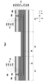
- FIG. 1 is an exploded perspective view of the multilayer substrate 10.
- FIG. 2 is a cross-sectional view of the multilayer substrate 10.
- FIG. 3 is a front view of the multilayer substrate 10 in use.
- FIG. 4 is an exploded perspective view of the multilayer substrate 10a.
- FIG. 5 is a top view of the liquid crystal polymer layers 16a, 17, and 16c of the multilayer substrate 10b.
- FIG. 6 is a cross-sectional view of the multilayer substrate 10c.
- FIG. 7 is a front view of the multilayer substrate 10c in use.
- FIG. 8 is a cross-sectional view of the multilayer substrate 10d.
- FIG. 9 is a cross-sectional view of the multilayer substrate 10e.
- FIG. 1 is an exploded perspective view of the multilayer substrate 10.
- FIG. 2 is a cross-sectional view of the multilayer substrate 10.
- FIG. 2 shows a cross section perpendicular to the front-rear direction.
- FIG. 3 is a front view of the multilayer substrate 10 in use.
- FIG. 1 only representative interlayer connection conductors v3 and v4 among the plurality of interlayer connection conductors v3 and v4 are given reference numerals.
- direction is defined as follows.
- the stacking direction of the stacked body 12 of the multilayer substrate 10 is defined as the vertical direction.
- the up-down direction coincides with the Z-axis direction.
- the upward direction is the positive direction of the Z axis.
- the downward direction is the negative direction of the Z axis.
- the direction in which the signal conductor layer 20 of the multilayer substrate 10 extends is defined as the left-right direction.
- the line width direction of the signal conductor layer 20 is defined as the front-back direction.
- the up-down direction, the front-back direction, and the left-right direction are orthogonal to each other. Note that the upper and lower directions in the vertical direction may be interchanged, the left and right directions in the horizontal direction may be interchanged, and the front and rear directions in the longitudinal direction may be interchanged.
- X is a component or member of the multilayer substrate 10.
- each part of X is defined as follows.
- the front part of the X means the front half of the X.
- the rear part of the X means the rear half of the X.
- the left part of X means the left half of X.
- the right side of X means the right half of X.
- the upper part of X means the upper half of X.
- the lower part of X means the lower half of X.
- the front end of X means the front end of X.
- the rear end of X means the end of X in the rear direction.
- the left end of X means the left end of X.
- the right end of X means the right end of X.
- the upper end of X means the upper end of X.
- the lower end of X means the lower end of X.
- the front end of X means the front end of X and its vicinity.
- the rear end of X means the rear end of X and its vicinity.
- the left end of X means the left end of X and its vicinity.
- the right end of X means the right end of X and its vicinity.
- the upper end of X means the upper end of X and its vicinity.
- the lower end of X means the lower end of X and its vicinity.
- Multilayer substrate 10 transmits high frequency signals.
- the multilayer substrate 10 is used to electrically connect two circuits in electronic devices such as smartphones.
- the multilayer board 10 includes a laminate 12, protective layers 18a and 18b, a signal conductor layer 20 (one or more conductor layers), a first ground conductor layer 22 (one or more conductor layers), and a second ground conductor layer 22 (one or more conductor layers).
- Ground conductor layer 24 (one or more conductor layers), signal terminals 26a, 26b (one or more conductor layers), connection conductor layers 28a, 28b (one or more conductor layers), interlayer connection conductors v1, v2, and a plurality of interlayer connections It is provided with conductors v3 and v4.
- the laminate 12 has a plate shape. Therefore, the laminate 12 has an upper main surface and a lower main surface.
- the upper main surface and the lower main surface of the laminate 12 have a rectangular shape with long sides extending in the left-right direction. Therefore, the length of the laminate 12 in the left-right direction is longer than the length of the laminate 12 in the front-rear direction.
- the laminate 12 has flexibility.
- the laminate 12 includes a liquid crystal polymer layer 16a (first liquid crystal polymer layer), a liquid crystal polymer layer 17 (second liquid crystal polymer layer), and a liquid crystal polymer layer 16c (third liquid crystal polymer layer). It has a structure in which polymer layers 16a to 16c and 17 are stacked in the Z-axis direction. The liquid crystal polymer layers 16a, 16b, 17, and 16c are arranged in this order from top to bottom. Therefore, the liquid crystal polymer layer 16a (first liquid crystal polymer layer) is located at the top of the liquid crystal polymer layers 16a to 16c and 17 (in the positive direction of the Z axis).
- the liquid crystal polymer layer 16c (third liquid crystal polymer layer) is located at the bottom of the liquid crystal polymer layers 16a to 16c and 17 (in the negative direction of the Z axis).
- the liquid crystal polymer layer 17 (second liquid crystal polymer layer) is located between the liquid crystal polymer layer 16a (first liquid crystal polymer layer) and the liquid crystal polymer layer 16c (third liquid crystal polymer layer) in the vertical direction (Z-axis direction). are doing.
- Each of the liquid crystal polymer layers 16a to 16c and the liquid crystal polymer layer 17 (second liquid crystal polymer layer) has an upper principal surface (a positive principal surface located in the positive direction of the Z axis) and a lower principal surface (a positive principal surface located in the negative direction of the Z axis). (negative principal surface).
- a material different from the liquid crystal polymer is provided between the liquid crystal polymer layer 16a and the liquid crystal polymer layer 16b, between the liquid crystal polymer layer 16b and the liquid crystal polymer layer 17, and between the liquid crystal polymer layer 17 and the liquid crystal polymer layer 16c.
- No insulator layer is provided. Therefore, the liquid crystal polymer layer 16a is in contact with the liquid crystal polymer layer 16b. The liquid crystal polymer layer 16a is fused to the liquid crystal polymer layer 16b. The liquid crystal polymer layer 16b is in contact with the liquid crystal polymer layer 17. The liquid crystal polymer layer 16b is fused to the liquid crystal polymer layer 17. The liquid crystal polymer layer 17 is in contact with the liquid crystal polymer layer 16c. The liquid crystal polymer layer 17 is fused to the liquid crystal polymer layer 16c.
- Gas permeation amount per unit volume of liquid crystal polymer layer 16a (first liquid crystal polymer layer), gas permeation amount per unit volume of liquid crystal polymer layer 16b, and gas per unit volume of liquid crystal polymer layer 16c (third liquid crystal polymer layer)
- the amount of gas permeation is greater than the amount of gas permeation per unit volume of the liquid crystal polymer layer 17 (second liquid crystal polymer layer).
- the amount of gas permeation refers to the amount of oxygen permeation at 25° C. (during use) and the amount of carbon dioxide permeation at 200° C. (during pressure bonding of the laminate).
- the amount of gas permeation is measured, for example, by the following procedure. First, a liquid crystal polymer layer having a predetermined thickness and area is prepared.
- Gas is filled in the space facing the upper main surface of the liquid crystal polymer layer, and the space facing the lower main surface of the liquid crystal polymer layer is brought into a vacuum state. Then, after a predetermined period of time has elapsed, the amount of gas present in the space facing the lower main surface of the liquid crystal polymer layer is measured.
- the gas is water vapor.
- the crystallinity of the liquid crystal polymer layer 17 is determined by the crystallinity of the liquid crystal polymer layer 16a (first liquid crystal polymer layer) and the crystallinity of the liquid crystal polymer layer 16b. and higher crystallinity than the liquid crystal polymer layer 16c (third liquid crystal polymer layer).
- the crystallinity of the liquid crystal polymer layer is measured by, for example, X-ray diffraction, DSC (suggestive operation calorimetry), FT-IR, solid-state NMR, or the like.
- the DSC is, for example, DSC3 manufactured by Mettler Toledo.
- the elastic modulus of the liquid crystal polymer layer 16a (first liquid crystal polymer layer), the elastic modulus of the liquid crystal polymer layer 16b, and the elastic modulus of the liquid crystal polymer layer 16c (third liquid crystal polymer layer) are the same as those of the liquid crystal polymer layer 17 (second liquid crystal polymer layer). layer) is lower than the elastic modulus of the layer.
- the material of the liquid crystal polymer layer 16a (first liquid crystal polymer layer), the material of the liquid crystal polymer layer 16b, and the material of the liquid crystal polymer layer 16c (third liquid crystal polymer layer) are, for example, 2 - A wholly aromatic polyester resin containing less than 50 mol% of hydroxy-6-naphthoic acid units.
- the material of the liquid crystal polymer layer 17 (second liquid crystal polymer layer) is, for example, a wholly aromatic polyester resin containing 50 mol % or more of 2-hydroxy-6-naphthoic acid units.
- the dielectric loss tangent of the liquid crystal polymer layer 17 is the dielectric loss tangent of the liquid crystal polymer layer 16a (first liquid crystal polymer layer), the dielectric loss tangent of the liquid crystal polymer layer 16b, and It is smaller than the dielectric loss tangent of the liquid crystal polymer layer 16c (third liquid crystal polymer layer).
- a high frequency signal is transmitted to the signal conductor layer 20.
- the signal conductor layer 20 (first conductor layer) is located between the liquid crystal polymer layer 17 (second liquid crystal polymer layer) and the liquid crystal polymer layer 16c (third liquid crystal polymer layer).
- the signal conductor layer 20 (first conductor layer, sixth conductor layer) is located on the lower main surface (negative main surface) of the liquid crystal polymer layer 17 (second liquid crystal polymer layer). Thereby, the signal conductor layer 20 (first conductor layer, internal conductor layer) is in contact with the liquid crystal polymer layer 17 (second liquid crystal polymer layer).
- the signal conductor layer 20 has a linear shape extending in the left-right direction.
- the first ground conductor layer 22 is provided on the laminate 12, as shown in FIG.
- the first ground conductor layer 22 is located above the signal conductor layer 20 (in the positive direction of the Z-axis) and overlaps with the signal conductor layer 20 when viewed in the vertical direction (Z-axis direction).
- the first ground conductor layer 22 is located on the upper main surface of the liquid crystal polymer layer 16a.
- the first ground conductor layer 22 (third conductor layer) is in contact with the liquid crystal polymer layer 16a (first liquid crystal polymer layer).
- the first ground conductor layer 22 covers substantially the entire upper main surface of the liquid crystal polymer layer 16a. Therefore, the area of the first ground conductor layer 22 (third conductor layer) is larger than the area of the signal conductor layer 20 (inner conductor layer).
- a ground potential is connected to the first ground conductor layer 22 .
- the second ground conductor layer 24 is provided on the laminate 12, as shown in FIG.
- the second ground conductor layer 24 is located below the signal conductor layer 20 (in the negative direction of the Z-axis) and overlaps with the signal conductor layer 20 when viewed in the vertical direction (Z-axis direction).
- the second ground conductor layer 24 is located on the lower main surface of the liquid crystal polymer layer 16c.
- the second ground conductor layer 24 (fourth conductor layer) is in contact with the liquid crystal polymer layer 16c (third liquid crystal polymer layer). Further, the second ground conductor layer 24 covers substantially the entire lower main surface of the liquid crystal polymer layer 16c.
- the area of the second ground conductor layer 24 (fourth conductor layer) is larger than the area of the signal conductor layer 20 (inner conductor layer).
- a ground potential is connected to the second ground conductor layer 24.
- the signal conductor layer 20, first ground conductor layer 22, and second ground conductor layer 24 as described above have a strip line structure.
- the signal terminal 26a is provided at the left end of the laminate 12. More specifically, the signal terminal 26a is located on the upper main surface of the liquid crystal polymer layer 16a. The signal terminal 26a overlaps the left end portion of the signal conductor layer 20 when viewed in the vertical direction. The signal terminal 26a has a rectangular shape when viewed in the vertical direction. The signal terminal 26a is an external terminal to which a high frequency signal is input/output. The signal terminal 26a is not in contact with the first ground conductor layer 22.
- connection conductor layer 28a is provided at the left end of the laminate 12. More specifically, the connecting conductor layer 28a (first conductor layer) is located between the liquid crystal polymer layer 16a (first liquid crystal polymer layer) and the liquid crystal polymer layer 17 (second liquid crystal polymer layer). In this embodiment, the connection conductor layer 28a is located on the lower main surface of the liquid crystal polymer layer 16b. In other words, the connection conductor layer 28a (first conductor layer, fifth conductor layer) is located on the upper main surface (front main surface) of the liquid crystal polymer layer 17 (second liquid crystal polymer layer). The connection conductor layer 28a overlaps the left end portion of the signal conductor layer 20 when viewed in the vertical direction. The connection conductor layer 28a has a rectangular shape when viewed in the vertical direction.
- the interlayer connection conductor v1 electrically connects the signal terminal 26a, the connection conductor layer 28a, and the left end portion of the signal conductor layer 20. More specifically, as shown in FIG. 2, the interlayer connection conductor v1 includes interlayer connection conductors v1a, v1b, and v1c.
- the interlayer connection conductor v1a vertically penetrates the liquid crystal polymer layer 16a.
- the interlayer connection conductor v1a is in contact with the signal terminal 26a. However, the interlayer connection conductor v1a does not penetrate the signal terminal 26a in the vertical direction.
- the interlayer connection conductor v1b vertically penetrates the liquid crystal polymer layer 16b.
- the interlayer connection conductor v1b is in contact with the interlayer connection conductor v1a and the connection conductor layer 28a. However, the interlayer connection conductor v1b does not penetrate the connection conductor layer 28a in the vertical direction.
- the interlayer connection conductor v1c vertically penetrates the liquid crystal polymer layer 17 (second liquid crystal polymer layer).
- the interlayer connection conductor v1c is in contact with the connection conductor layer 28a (fifth conductor layer) and the signal conductor layer 20 (sixth conductor layer). However, the interlayer connection conductor v1c does not penetrate the connection conductor layer 28a (fifth conductor layer) and the signal conductor layer 20 (sixth conductor layer) in the vertical direction (Z-axis direction).
- the structures of the signal terminal 26b, the connection conductor layer 28b, and the interlayer connection conductor v2 are laterally symmetrical to the structures of the signal terminal 26a, the connection conductor layer 28a, and the interlayer connection conductor v1, and therefore their explanation will be omitted.
- the plurality of interlayer connection conductors v3 are located before the signal conductor layer 20.
- the plurality of interlayer connection conductors v3 are lined up in a row in the left-right direction.
- the plurality of interlayer connection conductors v3 vertically penetrate the liquid crystal polymer layers 16a, 16b, 17, and 16c. Thereby, the plurality of interlayer connection conductors v3 electrically connect the first ground conductor layer 22 and the second ground conductor layer 24.
- the plurality of interlayer connection conductors v4 are located after the signal conductor layer 20.
- the plurality of interlayer connection conductors v4 are lined up in a row in the left-right direction.
- the plurality of interlayer connection conductors v4 vertically penetrate the liquid crystal polymer layers 16a, 16b, 17, and 16c. Thereby, the plurality of interlayer connection conductors v4 electrically connect the first ground conductor layer 22 and the second ground conductor layer 24.
- the first ground conductor layer 22, second ground conductor layer 24, signal terminals 26a, 26b, and connection conductor layers 28a, 28b as described above are, for example, the upper or lower principal surfaces of the liquid crystal polymer layers 16a to 16c, 17. It is formed by etching a metal foil provided on the surface.
- the metal foil is, for example, copper foil.
- the interlayer connection conductors v1 to v4 are, for example, via hole conductors.
- the via hole conductor is produced by forming through holes in the liquid crystal polymer layers 16a to 16c, 17, filling the through holes with conductive paste, and sintering the conductive paste.
- the material of the interlayer connection conductors v1 to v4 is a mixture of resin and metal. However, the material of the interlayer connection conductors v1 to v4 may contain metal and may not contain resin.
- the protective layer 18a (first protective layer) covers the upper main surface (the main surface in the positive direction of the Z-axis) of the laminate 12. Thereby, the protective layer 18a protects the first ground conductor layer 22.
- the protective layer 18a is provided with openings h1 to h6.
- the opening h1 overlaps the signal terminal 26a when viewed in the vertical direction. Thereby, the signal terminal 26a is exposed to the outside from the multilayer substrate 10.
- the opening h2 is located in front of the opening h1. A portion of the first ground conductor layer 22 is exposed to the outside from the multilayer substrate 10 via the opening h2.
- the opening h3 is located after the opening h1.
- a portion of the first ground conductor layer 22 is exposed to the outside from the multilayer substrate 10 via the opening h3. Thereby, a portion of the first ground conductor layer 22 functions as a ground terminal.
- the structure of the openings h4 to h6 is symmetrical to the structure of the openings h1 to h3, so a description thereof will be omitted.
- the protective layer 18b (second protective layer) covers the lower main surface (the main surface in the negative direction of the Z-axis) of the laminate 12. Thereby, the protective layer 18b protects the second ground conductor layer 24.
- the protective layers 18a and 18b as described above do not contain liquid crystal polymer. Therefore, the protective layers 18a, 18b are not part of the laminate 12.
- the protective layers 18a and 18b are, for example, resist layers. Further, the amount of gas permeation per unit volume of the protective layer 18a (first protective layer) and the amount of gas permeation per unit volume of the protective layer 18b (second protective layer) are the same as those of the liquid crystal polymer layer 16a (first liquid crystal polymer layer). The amount of gas permeation per unit volume of the liquid crystal polymer layer 16c (third liquid crystal polymer layer) is larger than that of the liquid crystal polymer layer 16c (third liquid crystal polymer layer).
- Such protective layers 18a and 18b are formed after the thermocompression bonding process of the laminate 12.
- the multilayer substrate 10 as described above has flexibility. Therefore, as shown in FIG. 3, the multilayer substrate 10 can be bent. Specifically, the multilayer substrate 10 has a first section A1, a second section A2, and a third section A3. The first section A1, the second section A2, and the third section A3 are arranged in this order from left to right when the multilayer substrate 10 is not bent. The second section A2 is bent downward with respect to the first section A1. On the other hand, the first section A1 and the third section A3 are not bent. However, the first section A1 and the third section A3 may be slightly bent. In this case, the radius of curvature of the first section A1 and the radius of curvature of the third section A3 are larger than the radius of curvature of the second section A2.
- gas generated inside the multilayer substrate 10 can be released to the outside of the multilayer substrate 10, and at the same time, it is possible to suppress air containing moisture from entering the inside of the multilayer substrate 10. More specifically, in the multilayer substrate 10, the amount of gas permeation per unit volume of the liquid crystal polymer layer 16a (first liquid crystal polymer layer) and the amount of gas permeation per unit volume of the liquid crystal polymer layer 16c (third liquid crystal polymer layer) are as follows. , is larger than the gas permeation amount per unit volume of the liquid crystal polymer layer 17 (second liquid crystal polymer layer). As a result, gas generated inside the multilayer substrate 10 during manufacturing is released to the outside of the multilayer substrate 10 via the liquid crystal polymer layers 16a and 16c. On the other hand, when the multilayer substrate 10 is used, the presence of the liquid crystal polymer layer 17 makes it difficult for air containing moisture to enter the multilayer substrate 10 . This reduces the moisture present in the liquid crystal polymer layer 17.
- the lower main surfaces of the connection conductor layers 28a and 28b (first conductor layer) located between the liquid crystal polymer layer 16a (first liquid crystal polymer layer) and the liquid crystal polymer layer 17 (second liquid crystal polymer layer) are as follows: It is located near the liquid crystal polymer layer 17.
- the lower main surfaces of the connection conductor layers 28a and 28b (first conductor layer) are in contact with the liquid crystal polymer layer 17. Therefore, when the moisture present in the liquid crystal polymer layer 17 is reduced, corrosion of the vicinity of the lower main surface of the connecting conductor layers 28a and 28b (first conductor layer) due to moisture is suppressed.
- the upper main surface of the signal conductor layer 20 located between the liquid crystal polymer layer 17 (second liquid crystal polymer layer) and the liquid crystal polymer layer 16c (third liquid crystal polymer layer) It is located near the polymer layer 17.
- the upper main surface of the signal conductor layer 20 (first conductor layer) is in contact with the liquid crystal polymer layer 17 . Therefore, when the moisture present in the liquid crystal polymer layer 17 is reduced, corrosion of the vicinity of the upper main surface of the signal conductor layer 20 due to moisture is suppressed.
- the multilayer substrate 10 is bent as shown in FIG. 3, a large tensile stress is applied to the liquid crystal polymer layer 16a, a large compressive stress is applied to the liquid crystal polymer layer 16c, and compressive stress and tensile stress are hardly applied to the liquid crystal polymer layer 17. . Therefore, the degree of crystallinity of the liquid crystal polymer layer 16a (first liquid crystal polymer layer) and the degree of crystallinity of the liquid crystal polymer layer 16c (third liquid crystal polymer layer) are the degree of crystallinity of the liquid crystal polymer layer 17 (second liquid crystal polymer layer). lower.
- the elastic modulus of the liquid crystal polymer layer 16a and the elastic modulus of the liquid crystal polymer layer 16c become lower than the elastic modulus of the liquid crystal polymer layer 17. Therefore, the liquid crystal polymer layers 16a, 16c are easily deformed, and damage to the liquid crystal polymer layers 16a, 16c is suppressed.
- the liquid crystal polymer layers 16a to 16c, 17 have a characteristic that they are easily plastically deformed by heating. However, the liquid crystal polymer layers 16a to 16c, 17 tend to generate gas when heated. Furthermore, when the multilayer substrate 10 is bent, it is preferable that the elastic modulus of the liquid crystal polymer layers 16a, 16c near the surface of the laminate 12 is low. Therefore, in the multilayer substrate 10, the crystallinity of the liquid crystal polymer layers 16a and 16c is low. Thereby, the gas generated in the laminate 12 is released to the outside of the laminate, and the laminate 12 becomes easier to bend.
- the material of the liquid crystal polymer layer 16a (first liquid crystal polymer layer), the material of the liquid crystal polymer layer 16b, and the material of the liquid crystal polymer layer 16c (third liquid crystal polymer layer) are, for example, 50 mol of 2-hydroxy-6-naphthoic acid units. % wholly aromatic polyester resin.
- the material of the liquid crystal polymer layer 17 (second liquid crystal polymer layer) is, for example, a wholly aromatic polyester resin containing 50 mol % or more of 2-hydroxy-6-naphthoic acid units.
- the amount of gas permeation per unit volume of the liquid crystal polymer layer 16a (first liquid crystal polymer layer) and the amount of gas permeation per unit volume of the liquid crystal polymer layer 16c (third liquid crystal polymer layer) are (2) liquid crystal polymer layer).
- the gas generated inside the multilayer substrate 10 can be released to the outside of the multilayer substrate 10, and at the same time, it is possible to suppress air containing moisture from entering the inside of the multilayer substrate 10.
- the signal conductor layer 20 is in contact with the liquid crystal polymer layer 17 (second liquid crystal polymer layer).
- the dielectric loss tangent of the liquid crystal polymer layer 17 (second liquid crystal polymer layer) is equal to the dielectric loss tangent of the liquid crystal polymer layer 16a (first liquid crystal polymer layer) and that of the liquid crystal polymer layer 16c (third liquid crystal polymer layer). smaller than the dielectric loss tangent. This reduces dielectric loss that occurs in high frequency signals transmitted through the signal conductor layer 20.
- the laminate 12 is produced by laminating the liquid crystal polymer layers 16a to 16c and 17 and then subjecting the liquid crystal polymer layers 16a to 16c and 17 to hot pressing. During this hot pressing, gas is generated within the laminate 12. Therefore, the signal conductor layer 20 (inner conductor layer) having a small area is in contact with the liquid crystal polymer layer 17 (second liquid crystal polymer layer) having a small amount of gas permeation.
- the first ground conductor layer 22 (third conductor layer) having a large area is in contact with the liquid crystal polymer layer 16a (first liquid crystal polymer layer) having a large amount of gas permeation.
- the second ground conductor layer 24 (fourth conductor layer) having a large area is in contact with the liquid crystal polymer layer 16c (third liquid crystal polymer layer) having a large amount of gas permeation.
- the gas in the liquid crystal polymer layer 17 is easily released to the outside of the multilayer substrate 10 because the liquid crystal polymer layer 17 is not largely covered by the signal conductor layer 20.
- peeling of the signal conductor layer 20 and the connection conductor layers 28a and 28b is suppressed.
- the liquid crystal polymer layers 16a and 16c are largely covered by the first ground conductor layer 22 and the second ground conductor layer 24, moisture-containing air is prevented from entering the inside of the multilayer substrate 10. .
- the amount of gas permeation per unit volume of the protective layer 18a (first protective layer) and the amount of gas permeation per unit volume of the protective layer 18b (second protective layer) are the same as those of the liquid crystal polymer layer 16a (first liquid crystal polymer layer).
- the amount of gas permeation per unit volume of the liquid crystal polymer layer 16c (third liquid crystal polymer layer) is larger than that of the liquid crystal polymer layer 16c (third liquid crystal polymer layer).
- the material of the interlayer connection conductor v1c is a mixture of resin and metal.
- Such an interlayer connection conductor v1c is hardened by heating during manufacturing. At this time, the interlayer connection conductor v1c generates gas.
- the interlayer connection conductor v1c does not penetrate the connection conductor layer 28a (fifth conductor layer) and the signal conductor layer 20 (sixth conductor layer) in the vertical direction (Z-axis direction). Therefore, gas is likely to be trapped between the connection conductor layer 28a (fifth conductor layer) and the signal conductor layer 20 (sixth conductor layer).
- the amount of gas permeation per unit volume of the liquid crystal polymer layer 16a (first liquid crystal polymer layer) and the amount of gas permeation per unit volume of the liquid crystal polymer layer 16c (third liquid crystal polymer layer) are This is larger than the amount of gas permeation per unit volume of layer 17 (second liquid crystal polymer layer).
- gas generated inside the multilayer substrate 10 during manufacturing is released to the outside of the multilayer substrate 10 via the liquid crystal polymer layers 16a and 16c.
- the liquid crystal polymer layer 17 makes it difficult for air containing moisture to enter the multilayer substrate 10 . This reduces the moisture present in the liquid crystal polymer layer 17.
- FIG. 4 is an exploded perspective view of the multilayer substrate 10a.
- the multilayer substrate 10a differs from the multilayer substrate 10 in that it further includes a third ground conductor layer 30.
- the third ground conductor layer 30 is located on the lower main surface of the liquid crystal polymer layer 17.
- the third ground conductor layer 30 covers most of the liquid crystal polymer layer 17.
- the third ground conductor layer 30 is insulated from the signal conductor layer 20.
- the third ground conductor layer 30 surrounds the signal conductor layer 20 when viewed in the vertical direction.
- the third ground conductor layer 30 is electrically connected to the first ground conductor layer 22 and the second ground conductor layer 24 via interlayer connection conductors v3 and v4. Therefore, the third ground conductor layer 30 is connected to the ground potential.
- the other structure of the multilayer substrate 10a is the same as that of the multilayer substrate 10, so the description thereof will be omitted.
- the multilayer substrate 10a can have the same effects as the multilayer substrate 10.
- FIG. 5 is a top view of the liquid crystal polymer layers 16a, 17, and 16c of the multilayer substrate 10b.
- the multilayer substrate 10b differs from the multilayer substrate 10a in that a plurality of holes ha to hc are provided. More specifically, the third ground conductor layer 30 (second conductor layer) is in contact with the liquid crystal polymer layer 17 (second liquid crystal polymer layer).
- the third ground conductor layer 30 (second conductor layer) is provided with a plurality of holes ha (first holes) that penetrate the third ground conductor layer 30 (second conductor layer) in the vertical direction (Z-axis direction). ing. At least some of the plurality of holes ha (first holes) have the same size and are arranged at regular intervals. In this embodiment, the plurality of holes ha are arranged in two rows. The plurality of holes ha are lined up in the left-right direction.
- the area of the hole ha (first hole) when viewed in the vertical direction (Z-axis direction) is smaller than the area of the interlayer connection conductors v1 to v4 when viewed in the vertical direction (Z-axis direction).
- the area of the interlayer connection conductors v1 to v4 when viewed in the vertical direction is the area of the region surrounded by the outer edges of the interlayer connection conductors v1 to v4 when viewed in the vertical direction.
- the hole ha is provided only in the third ground conductor layer 30 and not in the liquid crystal polymer layer 17.
- the hole ha is not a through hole in which metal is provided on the inner peripheral surface of a through hole that vertically penetrates the liquid crystal polymer layer 17.
- the first ground conductor layer 22 (third conductor layer) is in contact with the liquid crystal polymer layer 16a (first liquid crystal polymer layer).
- the first ground conductor layer 22 (third conductor layer) is provided with a plurality of holes hb (second holes) that penetrate the first ground conductor layer 22 (third conductor layer) in the vertical direction (Z-axis direction). ing. At least some of the plurality of holes hb (second holes) have the same size and are arranged at equal intervals. In this embodiment, the plurality of holes hb are arranged in two rows. The plurality of holes hb are lined up in the left-right direction. The area of the hole hb (second hole) viewed in the vertical direction (Z-axis direction) is smaller than the area of the hole ha (first hole) viewed in the vertical direction (Z-axis direction).
- the second ground conductor layer 24 (fourth conductor layer) is in contact with the liquid crystal polymer layer 16c (third liquid crystal polymer layer).
- the second ground conductor layer 24 (fourth conductor layer) is provided with a plurality of holes hc (third holes) that penetrate the second ground conductor layer 24 (fourth conductor layer) in the vertical direction (Z-axis direction). ing. At least some of the plurality of holes hc (third holes) have the same size and are arranged at equal intervals. In this embodiment, the plurality of holes hc are arranged in two rows. The plurality of holes hc are lined up in the left-right direction.
- the area of the hole hc (third hole) seen in the up-down direction (Z-axis direction) is smaller than the area of the hole ha (first hole) seen in the up-down direction (Z-axis direction).
- the other structure of the multilayer substrate 10b is the same as that of the multilayer substrate 10a, so a description thereof will be omitted.
- the multilayer substrate 10b can have the same effects as the multilayer substrate 10a.
- the area of hole hb (second hole) viewed in the vertical direction (Z-axis direction) or the area of hole hc (third hole) viewed in the vertical direction (Z-axis direction) is direction) is smaller than the area of the hole ha (first hole). This suppresses noise from leaking through the liquid crystal polymer layer 16a.
- the areas of the holes hb provided in the first ground conductor layer 22 and the holes hc provided in the second ground conductor layer 24 are small, noise is suppressed from being radiated from the multilayer substrate 10b, and , noise is suppressed from entering the multilayer substrate 10b. Furthermore, the potentials of the first ground conductor layer 22 and the second ground conductor layer 24 become stable at the ground potential.
- FIG. 6 is a cross-sectional view of the multilayer substrate 10c.
- FIG. 7 is a front view of the multilayer substrate 10c in use.
- the multilayer substrate 10c differs from the multilayer substrate 10c in that the vertical thickness of the second section A2 is smaller than the vertical thickness of the first section A1 and the vertical thickness of the third section A3.
- liquid crystal polymer layers 16a, 16b, and 17 are not present.
- the second section A2 becomes easier to deform than the first section A1 and the third section A3. That is, the second section A2 functions as a flexible area.
- the first section A1 and the third section A3 function as rigid regions. As shown in FIG. 7, the second section A2 is bent downward with respect to the first section A1.
- the other structure of the multilayer substrate 10c is the same as that of the multilayer substrate 10, so a description thereof will be omitted.
- the multilayer substrate 10c can have the same effects as the multilayer substrate 10.
- the liquid crystal polymer layer 17 with a high elastic modulus does not exist in the second section A2. This makes it easier for the second section A2 to bend.
- the elastic modulus is the elastic modulus at room temperature.
- the normal temperature is, for example, 5°C or higher and 35°C or lower.
- FIG. 8 is a cross-sectional view of the multilayer substrate 10d.
- the multilayer substrate 10d differs from the multilayer substrate 10 in that the liquid crystal polymer layer 17 is not provided in the second section A2. In this way, the liquid crystal polymer layer 17 having a high elastic modulus does not exist in the second section A2. This makes it easier for the second section A2 to bend.
- the other structure of the multilayer substrate 10d is the same as that of the multilayer substrate 10, so the description thereof will be omitted.
- the multilayer substrate 10d can have the same effects as the multilayer substrate 10.
- FIG. 9 is a cross-sectional view of the multilayer substrate 10e.
- the multilayer substrate 10e differs from the multilayer substrate 10c in that the laminate 12 further includes liquid crystal polymer layers 17a and 17b. More specifically, the liquid crystal polymer layer 17a is laminated on the liquid crystal polymer layer 17. The liquid crystal polymer layer 17b is laminated below the liquid crystal polymer layer 17. In this way, a plurality of liquid crystal polymer layers having a small amount of gas permeation may be provided. As a result, the signal conductor layer 20 is sandwiched between the liquid crystal polymer layers 17 and 17b having low gas permeability from above and below. As a result, corrosion of the signal conductor layer 20 is suppressed.
- the other structure of the multilayer substrate 10e is the same as that of the multilayer substrate 10, so the description thereof will be omitted.
- the multilayer substrate 10e can have the same effects as the multilayer substrate 10.
- the multilayer substrate according to the present invention is not limited to the multilayer substrates 10, 10a to 10e, and can be modified within the scope of the gist. Note that the structures of the multilayer substrates 10, 10a to 10e may be combined arbitrarily.
- protective layers 18a and 18b are not essential components. Further, either the protective layer 18a or the protective layer 18b may be provided.
- first ground conductor layer 22 and the second ground conductor layer 24 are not essential components. Further, either the first ground conductor layer 22 or the second ground conductor layer 24 may be provided.
- the liquid crystal polymer layers 16a to 16c, 17 may be made of the same material.
- the liquid crystal polymer layers 16a to 16c, 17 are made of, for example, a porous material. It is sufficient that the porosity of the liquid crystal polymer layer 17 is lower than that of the liquid crystal polymer layers 16a to 16c. As a result, the amount of gas permeation per unit volume of the liquid crystal polymer layers 16a to 16c becomes greater than the amount of gas permeation per unit volume of the liquid crystal polymer layer 17. As a result, the gas within the stacked body 12 is released to the outside of the stacked body 12.
- the first conductor layer may be located only on one side between the two layers.
- interlayer connection conductors v1 to v4 do not have to be via hole conductors.
- the interlayer connection conductors v1 to v4 may be through-hole conductors.
- the through-hole conductor is formed by plating the inner peripheral surface of a through-hole that vertically penetrates the liquid crystal polymer layer.
- the protective layers 18a and 18b are provided for the purpose of suppressing corrosion of the conductor layer due to exposure of the conductor layer. Therefore, the amount of gas permeation per unit volume of the protective layers 18a, 18b does not need to be larger than the amount of gas permeation per unit volume of the liquid crystal polymer layers 16a, 16c. Therefore, the amount of gas permeation per unit volume of the protective layers 18a, 18b may be less than the amount of gas permeation per unit volume of the liquid crystal polymer layers 16a, 16c.
- connection conductor v1c may penetrate the connection conductor layer 28a (fifth conductor layer) and the signal conductor layer 20 (sixth conductor layer) in the vertical direction (Z-axis direction).
- a liquid crystal polymer layer may be provided between the liquid crystal polymer layer 17a and the liquid crystal polymer layer 17. Further, a liquid crystal polymer layer may be provided between the liquid crystal polymer layer 17 and the liquid crystal polymer layer 17b.
- This liquid crystal polymer has a gas permeation amount that is greater than the gas permeation amount per unit volume of the liquid crystal polymer layers 17, 17a, and 17b.
- the plurality of holes Ha may be provided in a conductor layer other than the third ground conductor layer 30, and only need to be provided in a conductor layer provided in the laminate 12.
- Multilayer substrate 12 Laminated bodies 16a to 16c, 17, 17a, 17b: Liquid crystal polymer layers 18a, 18b: Protective layer 20: Signal conductor layer 22: First ground conductor layer 24: Second ground conductor layer 26a, 26b: Signal terminals 28a, 28b: Connection conductor layer 30: Third ground conductor layer A1: First section A2: Second section A3: Third section ha-hc: Holes v1-v4, v1a-v1c: Interlayer connection conductor
Landscapes
- Physics & Mathematics (AREA)
- Nonlinear Science (AREA)
- General Physics & Mathematics (AREA)
- Optics & Photonics (AREA)
- Chemical & Material Sciences (AREA)
- Crystallography & Structural Chemistry (AREA)
- Engineering & Computer Science (AREA)
- Mathematical Physics (AREA)
- Mechanical Engineering (AREA)
- Microelectronics & Electronic Packaging (AREA)
- Manufacturing & Machinery (AREA)
- Production Of Multi-Layered Print Wiring Board (AREA)
- Devices For Indicating Variable Information By Combining Individual Elements (AREA)
Priority Applications (3)
| Application Number | Priority Date | Filing Date | Title |
|---|---|---|---|
| CN202390000198.6U CN222381883U (zh) | 2022-04-14 | 2023-03-16 | 多层基板 |
| JP2024514863A JP7747185B2 (ja) | 2022-04-14 | 2023-03-16 | 多層基板 |
| US18/766,841 US20240359445A1 (en) | 2022-04-14 | 2024-07-09 | Multilayer substrate |
Applications Claiming Priority (2)
| Application Number | Priority Date | Filing Date | Title |
|---|---|---|---|
| JP2022-066670 | 2022-04-14 | ||
| JP2022066670 | 2022-04-14 |
Related Child Applications (1)
| Application Number | Title | Priority Date | Filing Date |
|---|---|---|---|
| US18/766,841 Continuation US20240359445A1 (en) | 2022-04-14 | 2024-07-09 | Multilayer substrate |
Publications (1)
| Publication Number | Publication Date |
|---|---|
| WO2023199693A1 true WO2023199693A1 (ja) | 2023-10-19 |
Family
ID=88329406
Family Applications (1)
| Application Number | Title | Priority Date | Filing Date |
|---|---|---|---|
| PCT/JP2023/010391 Ceased WO2023199693A1 (ja) | 2022-04-14 | 2023-03-16 | 多層基板 |
Country Status (4)
| Country | Link |
|---|---|
| US (1) | US20240359445A1 (https=) |
| JP (1) | JP7747185B2 (https=) |
| CN (1) | CN222381883U (https=) |
| WO (1) | WO2023199693A1 (https=) |
Citations (4)
| Publication number | Priority date | Publication date | Assignee | Title |
|---|---|---|---|---|
| JP2013005549A (ja) * | 2011-06-15 | 2013-01-07 | Hitachi Ltd | ガス絶縁開閉装置 |
| WO2018079479A1 (ja) * | 2016-10-27 | 2018-05-03 | 株式会社村田製作所 | 多層基板およびその製造方法 |
| WO2019098012A1 (ja) * | 2017-11-16 | 2019-05-23 | 株式会社村田製作所 | 樹脂多層基板、電子部品およびその実装構造 |
| WO2020122180A1 (ja) * | 2018-12-13 | 2020-06-18 | 株式会社村田製作所 | 樹脂多層基板および電子機器 |
-
2023
- 2023-03-16 CN CN202390000198.6U patent/CN222381883U/zh active Active
- 2023-03-16 WO PCT/JP2023/010391 patent/WO2023199693A1/ja not_active Ceased
- 2023-03-16 JP JP2024514863A patent/JP7747185B2/ja active Active
-
2024
- 2024-07-09 US US18/766,841 patent/US20240359445A1/en active Pending
Patent Citations (4)
| Publication number | Priority date | Publication date | Assignee | Title |
|---|---|---|---|---|
| JP2013005549A (ja) * | 2011-06-15 | 2013-01-07 | Hitachi Ltd | ガス絶縁開閉装置 |
| WO2018079479A1 (ja) * | 2016-10-27 | 2018-05-03 | 株式会社村田製作所 | 多層基板およびその製造方法 |
| WO2019098012A1 (ja) * | 2017-11-16 | 2019-05-23 | 株式会社村田製作所 | 樹脂多層基板、電子部品およびその実装構造 |
| WO2020122180A1 (ja) * | 2018-12-13 | 2020-06-18 | 株式会社村田製作所 | 樹脂多層基板および電子機器 |
Also Published As
| Publication number | Publication date |
|---|---|
| CN222381883U (zh) | 2025-01-21 |
| US20240359445A1 (en) | 2024-10-31 |
| JP7747185B2 (ja) | 2025-10-01 |
| JPWO2023199693A1 (https=) | 2023-10-19 |
Similar Documents
| Publication | Publication Date | Title |
|---|---|---|
| CN205093042U (zh) | 柔性电路基板 | |
| US8609991B2 (en) | Flex-rigid wiring board and method for manufacturing the same | |
| US5136123A (en) | Multilayer circuit board | |
| CN205081202U (zh) | 传输线路及扁平电缆 | |
| CN103733736B (zh) | 高频信号传输线路及电子设备 | |
| WO2014002757A1 (ja) | ケーブルの接続・固定方法 | |
| CN105792501A (zh) | 电路板及其制作方法 | |
| JP6841342B2 (ja) | 樹脂多層基板、電子部品およびその実装構造 | |
| JP2001111218A (ja) | 多層プリント回路基板および電子装置 | |
| JPWO2019098012A1 (ja) | 樹脂多層基板、電子部品およびその実装構造 | |
| CN104427740B (zh) | 电路板及其制作方法 | |
| JP2006019345A (ja) | フレキシブルプリント配線板 | |
| US9318786B2 (en) | High-frequency signal line and electronic device | |
| WO2023199693A1 (ja) | 多層基板 | |
| JPH11176253A (ja) | フラット型ケーブル | |
| JP2019145765A (ja) | プリント回路基板 | |
| JP7597128B2 (ja) | 多層基板及び多層基板の製造方法 | |
| WO2023171351A1 (ja) | 回路基板及び回路基板の製造方法 | |
| WO2017077837A1 (ja) | 部品実装基板 | |
| JP7827160B2 (ja) | アンテナモジュール | |
| US20250365857A1 (en) | Multilayer substrate, electronic device, and method for manufacturing multilayer substrate | |
| CN219718562U (zh) | 多层基板以及电子设备 | |
| JP7287462B2 (ja) | 樹脂多層基板 | |
| CN121909565A (zh) | 微波同轴中介层 | |
| JP4795863B2 (ja) | 配線基板内蔵用コンデンサの製造方法、配線基板内蔵用コンデンサ、及び配線基板 |
Legal Events
| Date | Code | Title | Description |
|---|---|---|---|
| 121 | Ep: the epo has been informed by wipo that ep was designated in this application |
Ref document number: 23788115 Country of ref document: EP Kind code of ref document: A1 |
|
| WWE | Wipo information: entry into national phase |
Ref document number: 2024514863 Country of ref document: JP |
|
| WWE | Wipo information: entry into national phase |
Ref document number: 202390000198.6 Country of ref document: CN |
|
| NENP | Non-entry into the national phase |
Ref country code: DE |
|
| WWP | Wipo information: published in national office |
Ref document number: 202390000198.6 Country of ref document: CN |
|
| 122 | Ep: pct application non-entry in european phase |
Ref document number: 23788115 Country of ref document: EP Kind code of ref document: A1 |