WO2023182194A1 - 半導体基板の製造方法および製造装置 - Google Patents
半導体基板の製造方法および製造装置 Download PDFInfo
- Publication number
- WO2023182194A1 WO2023182194A1 PCT/JP2023/010518 JP2023010518W WO2023182194A1 WO 2023182194 A1 WO2023182194 A1 WO 2023182194A1 JP 2023010518 W JP2023010518 W JP 2023010518W WO 2023182194 A1 WO2023182194 A1 WO 2023182194A1
- Authority
- WO
- WIPO (PCT)
- Prior art keywords
- nitride semiconductor
- light
- semiconductor
- growth
- manufacturing
- Prior art date
- Legal status (The legal status is an assumption and is not a legal conclusion. Google has not performed a legal analysis and makes no representation as to the accuracy of the status listed.)
- Ceased
Links
Images





Classifications
-
- H—ELECTRICITY
- H10—SEMICONDUCTOR DEVICES; ELECTRIC SOLID-STATE DEVICES NOT OTHERWISE PROVIDED FOR
- H10P—GENERIC PROCESSES OR APPARATUS FOR THE MANUFACTURE OR TREATMENT OF DEVICES COVERED BY CLASS H10
- H10P14/00—Formation of materials, e.g. in the shape of layers or pillars
- H10P14/20—Formation of materials, e.g. in the shape of layers or pillars of semiconductor materials
- H10P14/27—Formation of materials, e.g. in the shape of layers or pillars of semiconductor materials using selective deposition, e.g. simultaneous growth of monocrystalline and non-monocrystalline semiconductor materials
- H10P14/271—Formation of materials, e.g. in the shape of layers or pillars of semiconductor materials using selective deposition, e.g. simultaneous growth of monocrystalline and non-monocrystalline semiconductor materials characterised by the preparation of substrate for selective deposition
-
- C—CHEMISTRY; METALLURGY
- C30—CRYSTAL GROWTH
- C30B—SINGLE-CRYSTAL GROWTH; UNIDIRECTIONAL SOLIDIFICATION OF EUTECTIC MATERIAL OR UNIDIRECTIONAL DEMIXING OF EUTECTOID MATERIAL; REFINING BY ZONE-MELTING OF MATERIAL; PRODUCTION OF A HOMOGENEOUS POLYCRYSTALLINE MATERIAL WITH DEFINED STRUCTURE; SINGLE CRYSTALS OR HOMOGENEOUS POLYCRYSTALLINE MATERIAL WITH DEFINED STRUCTURE; AFTER-TREATMENT OF SINGLE CRYSTALS OR A HOMOGENEOUS POLYCRYSTALLINE MATERIAL WITH DEFINED STRUCTURE; APPARATUS THEREFOR
- C30B25/00—Single-crystal growth by chemical reaction of reactive gases, e.g. chemical vapour-deposition growth
- C30B25/02—Epitaxial-layer growth
- C30B25/04—Pattern deposit, e.g. by using masks
-
- C—CHEMISTRY; METALLURGY
- C30—CRYSTAL GROWTH
- C30B—SINGLE-CRYSTAL GROWTH; UNIDIRECTIONAL SOLIDIFICATION OF EUTECTIC MATERIAL OR UNIDIRECTIONAL DEMIXING OF EUTECTOID MATERIAL; REFINING BY ZONE-MELTING OF MATERIAL; PRODUCTION OF A HOMOGENEOUS POLYCRYSTALLINE MATERIAL WITH DEFINED STRUCTURE; SINGLE CRYSTALS OR HOMOGENEOUS POLYCRYSTALLINE MATERIAL WITH DEFINED STRUCTURE; AFTER-TREATMENT OF SINGLE CRYSTALS OR A HOMOGENEOUS POLYCRYSTALLINE MATERIAL WITH DEFINED STRUCTURE; APPARATUS THEREFOR
- C30B25/00—Single-crystal growth by chemical reaction of reactive gases, e.g. chemical vapour-deposition growth
- C30B25/02—Epitaxial-layer growth
- C30B25/14—Feed and outlet means for the gases; Modifying the flow of the reactive gases
-
- C—CHEMISTRY; METALLURGY
- C30—CRYSTAL GROWTH
- C30B—SINGLE-CRYSTAL GROWTH; UNIDIRECTIONAL SOLIDIFICATION OF EUTECTIC MATERIAL OR UNIDIRECTIONAL DEMIXING OF EUTECTOID MATERIAL; REFINING BY ZONE-MELTING OF MATERIAL; PRODUCTION OF A HOMOGENEOUS POLYCRYSTALLINE MATERIAL WITH DEFINED STRUCTURE; SINGLE CRYSTALS OR HOMOGENEOUS POLYCRYSTALLINE MATERIAL WITH DEFINED STRUCTURE; AFTER-TREATMENT OF SINGLE CRYSTALS OR A HOMOGENEOUS POLYCRYSTALLINE MATERIAL WITH DEFINED STRUCTURE; APPARATUS THEREFOR
- C30B25/00—Single-crystal growth by chemical reaction of reactive gases, e.g. chemical vapour-deposition growth
- C30B25/02—Epitaxial-layer growth
- C30B25/16—Controlling or regulating
-
- C—CHEMISTRY; METALLURGY
- C30—CRYSTAL GROWTH
- C30B—SINGLE-CRYSTAL GROWTH; UNIDIRECTIONAL SOLIDIFICATION OF EUTECTIC MATERIAL OR UNIDIRECTIONAL DEMIXING OF EUTECTOID MATERIAL; REFINING BY ZONE-MELTING OF MATERIAL; PRODUCTION OF A HOMOGENEOUS POLYCRYSTALLINE MATERIAL WITH DEFINED STRUCTURE; SINGLE CRYSTALS OR HOMOGENEOUS POLYCRYSTALLINE MATERIAL WITH DEFINED STRUCTURE; AFTER-TREATMENT OF SINGLE CRYSTALS OR A HOMOGENEOUS POLYCRYSTALLINE MATERIAL WITH DEFINED STRUCTURE; APPARATUS THEREFOR
- C30B25/00—Single-crystal growth by chemical reaction of reactive gases, e.g. chemical vapour-deposition growth
- C30B25/02—Epitaxial-layer growth
- C30B25/16—Controlling or regulating
- C30B25/165—Controlling or regulating the flow of the reactive gases
-
- C—CHEMISTRY; METALLURGY
- C30—CRYSTAL GROWTH
- C30B—SINGLE-CRYSTAL GROWTH; UNIDIRECTIONAL SOLIDIFICATION OF EUTECTIC MATERIAL OR UNIDIRECTIONAL DEMIXING OF EUTECTOID MATERIAL; REFINING BY ZONE-MELTING OF MATERIAL; PRODUCTION OF A HOMOGENEOUS POLYCRYSTALLINE MATERIAL WITH DEFINED STRUCTURE; SINGLE CRYSTALS OR HOMOGENEOUS POLYCRYSTALLINE MATERIAL WITH DEFINED STRUCTURE; AFTER-TREATMENT OF SINGLE CRYSTALS OR A HOMOGENEOUS POLYCRYSTALLINE MATERIAL WITH DEFINED STRUCTURE; APPARATUS THEREFOR
- C30B25/00—Single-crystal growth by chemical reaction of reactive gases, e.g. chemical vapour-deposition growth
- C30B25/02—Epitaxial-layer growth
- C30B25/18—Epitaxial-layer growth characterised by the substrate
-
- C—CHEMISTRY; METALLURGY
- C30—CRYSTAL GROWTH
- C30B—SINGLE-CRYSTAL GROWTH; UNIDIRECTIONAL SOLIDIFICATION OF EUTECTIC MATERIAL OR UNIDIRECTIONAL DEMIXING OF EUTECTOID MATERIAL; REFINING BY ZONE-MELTING OF MATERIAL; PRODUCTION OF A HOMOGENEOUS POLYCRYSTALLINE MATERIAL WITH DEFINED STRUCTURE; SINGLE CRYSTALS OR HOMOGENEOUS POLYCRYSTALLINE MATERIAL WITH DEFINED STRUCTURE; AFTER-TREATMENT OF SINGLE CRYSTALS OR A HOMOGENEOUS POLYCRYSTALLINE MATERIAL WITH DEFINED STRUCTURE; APPARATUS THEREFOR
- C30B29/00—Single crystals or homogeneous polycrystalline material with defined structure characterised by the material or by their shape
- C30B29/10—Inorganic compounds or compositions
- C30B29/38—Nitrides
-
- H—ELECTRICITY
- H10—SEMICONDUCTOR DEVICES; ELECTRIC SOLID-STATE DEVICES NOT OTHERWISE PROVIDED FOR
- H10P—GENERIC PROCESSES OR APPARATUS FOR THE MANUFACTURE OR TREATMENT OF DEVICES COVERED BY CLASS H10
- H10P14/00—Formation of materials, e.g. in the shape of layers or pillars
- H10P14/20—Formation of materials, e.g. in the shape of layers or pillars of semiconductor materials
- H10P14/24—Formation of materials, e.g. in the shape of layers or pillars of semiconductor materials using chemical vapour deposition [CVD]
-
- H—ELECTRICITY
- H10—SEMICONDUCTOR DEVICES; ELECTRIC SOLID-STATE DEVICES NOT OTHERWISE PROVIDED FOR
- H10P—GENERIC PROCESSES OR APPARATUS FOR THE MANUFACTURE OR TREATMENT OF DEVICES COVERED BY CLASS H10
- H10P14/00—Formation of materials, e.g. in the shape of layers or pillars
- H10P14/20—Formation of materials, e.g. in the shape of layers or pillars of semiconductor materials
- H10P14/27—Formation of materials, e.g. in the shape of layers or pillars of semiconductor materials using selective deposition, e.g. simultaneous growth of monocrystalline and non-monocrystalline semiconductor materials
- H10P14/276—Lateral overgrowth
-
- H—ELECTRICITY
- H10—SEMICONDUCTOR DEVICES; ELECTRIC SOLID-STATE DEVICES NOT OTHERWISE PROVIDED FOR
- H10P—GENERIC PROCESSES OR APPARATUS FOR THE MANUFACTURE OR TREATMENT OF DEVICES COVERED BY CLASS H10
- H10P14/00—Formation of materials, e.g. in the shape of layers or pillars
- H10P14/20—Formation of materials, e.g. in the shape of layers or pillars of semiconductor materials
- H10P14/32—Formation of materials, e.g. in the shape of layers or pillars of semiconductor materials characterised by intermediate layers between substrates and deposited layers
- H10P14/3202—Materials thereof
- H10P14/3214—Materials thereof being Group IIIA-VA semiconductors
- H10P14/3216—Nitrides
-
- H—ELECTRICITY
- H10—SEMICONDUCTOR DEVICES; ELECTRIC SOLID-STATE DEVICES NOT OTHERWISE PROVIDED FOR
- H10P—GENERIC PROCESSES OR APPARATUS FOR THE MANUFACTURE OR TREATMENT OF DEVICES COVERED BY CLASS H10
- H10P14/00—Formation of materials, e.g. in the shape of layers or pillars
- H10P14/20—Formation of materials, e.g. in the shape of layers or pillars of semiconductor materials
- H10P14/34—Deposited materials, e.g. layers
- H10P14/3402—Deposited materials, e.g. layers characterised by the chemical composition
- H10P14/3414—Deposited materials, e.g. layers characterised by the chemical composition being group IIIA-VIA materials
- H10P14/3416—Nitrides
-
- H—ELECTRICITY
- H10—SEMICONDUCTOR DEVICES; ELECTRIC SOLID-STATE DEVICES NOT OTHERWISE PROVIDED FOR
- H10P—GENERIC PROCESSES OR APPARATUS FOR THE MANUFACTURE OR TREATMENT OF DEVICES COVERED BY CLASS H10
- H10P14/00—Formation of materials, e.g. in the shape of layers or pillars
- H10P14/20—Formation of materials, e.g. in the shape of layers or pillars of semiconductor materials
- H10P14/29—Formation of materials, e.g. in the shape of layers or pillars of semiconductor materials characterised by the substrates
- H10P14/2901—Materials
- H10P14/2902—Materials being Group IVA materials
- H10P14/2904—Silicon carbide
-
- H—ELECTRICITY
- H10—SEMICONDUCTOR DEVICES; ELECTRIC SOLID-STATE DEVICES NOT OTHERWISE PROVIDED FOR
- H10P—GENERIC PROCESSES OR APPARATUS FOR THE MANUFACTURE OR TREATMENT OF DEVICES COVERED BY CLASS H10
- H10P14/00—Formation of materials, e.g. in the shape of layers or pillars
- H10P14/20—Formation of materials, e.g. in the shape of layers or pillars of semiconductor materials
- H10P14/29—Formation of materials, e.g. in the shape of layers or pillars of semiconductor materials characterised by the substrates
- H10P14/2901—Materials
- H10P14/2902—Materials being Group IVA materials
- H10P14/2905—Silicon, silicon germanium or germanium
-
- H—ELECTRICITY
- H10—SEMICONDUCTOR DEVICES; ELECTRIC SOLID-STATE DEVICES NOT OTHERWISE PROVIDED FOR
- H10P—GENERIC PROCESSES OR APPARATUS FOR THE MANUFACTURE OR TREATMENT OF DEVICES COVERED BY CLASS H10
- H10P14/00—Formation of materials, e.g. in the shape of layers or pillars
- H10P14/20—Formation of materials, e.g. in the shape of layers or pillars of semiconductor materials
- H10P14/29—Formation of materials, e.g. in the shape of layers or pillars of semiconductor materials characterised by the substrates
- H10P14/2901—Materials
- H10P14/2921—Materials being crystalline insulating materials
-
- H—ELECTRICITY
- H10—SEMICONDUCTOR DEVICES; ELECTRIC SOLID-STATE DEVICES NOT OTHERWISE PROVIDED FOR
- H10P—GENERIC PROCESSES OR APPARATUS FOR THE MANUFACTURE OR TREATMENT OF DEVICES COVERED BY CLASS H10
- H10P14/00—Formation of materials, e.g. in the shape of layers or pillars
- H10P14/20—Formation of materials, e.g. in the shape of layers or pillars of semiconductor materials
- H10P14/29—Formation of materials, e.g. in the shape of layers or pillars of semiconductor materials characterised by the substrates
- H10P14/2926—Crystal orientations
Definitions
- the present disclosure relates to a method and apparatus for manufacturing a semiconductor substrate.
- Patent Document 1 discloses a method of forming a GaN-based semiconductor layer on a GaN-based substrate or a different type of substrate (for example, a sapphire substrate) using the ELO (Epitaxial Lateral Overgrowth) method.
- a method for manufacturing a semiconductor substrate includes a step of preparing a template substrate including a base substrate and having a growth suppression region and first and second seed regions, and a first nitride semiconductor portion from the first seed region. a step of growing a second nitride semiconductor portion from the second seed region above the growth suppressing region; a step of irradiating a semiconductor substrate including a semiconductor section with first light; a step of receiving second light from the semiconductor substrate; and a step of irradiating the first and second nitride semiconductor sections before the first and second nitride semiconductor sections meet. 2. A step of stopping the growth of the nitride semiconductor portion is performed.
- FIG. 1 is a cross-sectional view showing the configuration of a semiconductor substrate according to this embodiment.
- 3 is a flowchart showing a method for manufacturing a semiconductor substrate according to the present embodiment.
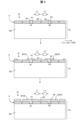
- FIG. 2 is a cross-sectional view showing a method for manufacturing a semiconductor substrate according to the present embodiment.
- 1 is a cross-sectional view showing the configuration of a semiconductor substrate of this embodiment.
- 2 is a graph showing changes in reflectance of a semiconductor substrate over time (when the wavelengths of the first light are 405 nm and 633 nm). It is a graph which shows the relationship between the inclination angle of an inclination area
- 3 is a graph showing temporal changes in gap widths of first and second nitride semiconductor parts.
- FIG. 2 is a cross-sectional view showing an example of the shape of a nitride semiconductor portion having an inclined region. It is a graph showing a change in reflectance of a semiconductor substrate over time. It is a graph showing a change in reflectance of a semiconductor substrate over time. 11 is a graph showing the vicinity of the inflection point in FIG. 10.
- FIG. 3 is a cross-sectional view showing changes in shape of side facets of each of the first and second nitride semiconductor parts. It is a top view showing an example of a mask.
- FIG. 3 is a cross-sectional view showing an example of the configuration of a base substrate.
- FIG. 3 is a cross-sectional view showing an example of the configuration of a base portion.
- FIG. 7 is a cross-sectional view showing another example of the method for manufacturing a semiconductor substrate according to the present embodiment.
- FIG. 1 is a schematic diagram showing the configuration of a semiconductor substrate manufacturing apparatus according to the present embodiment. 1 is a cross-sectional view showing a method for manufacturing a semiconductor substrate according to Example 1.
- FIG. 3 is a cross-sectional view showing a method for manufacturing a semiconductor device according to Example 2.
- FIG. 3 is a schematic diagram showing the configuration of a semiconductor substrate manufacturing apparatus according to Example 3.
- FIG. FIG. 2 is a cross-sectional view showing a method for manufacturing a semiconductor substrate according to the present embodiment.
- FIG. 1 is a cross-sectional view showing the structure of a semiconductor substrate according to this embodiment.
- a semiconductor substrate 10 semiconductor wafer
- a semiconductor substrate TS semiconductor wafer
- the first nitride semiconductor section 8F is arranged above the growth suppression region SP from the first seed region 4F
- the second nitride semiconductor section 8S is arranged above the growth suppression region SP from the second seed region 4S.
- the template substrate TS has a mask portion 5 and a mask pattern 6 having a first opening K1 and a second opening K2 on a base substrate BS.
- the upper surface of the mask portion 5 is a growth suppression region SP, and a first seed region 4F overlapping with the first opening K1 and a second seed region 4F overlapping with the second opening K2 are located on the upper surface of the base substrate BS. You can leave it there.
- the first and second nitride semiconductor parts 8F and 8S are adjacent to each other with a gap GP in between.
- the first and second seed regions 4F and 4S will be collectively referred to as seed region 4
- the first and second openings K1 and K2 will be collectively referred to as opening K
- the first and second nitride semiconductor regions 8F and 8S will be collectively referred to as seed region 4. It may be collectively referred to as nitride semiconductor section 8.
- the nitride semiconductor portion 8 may be a nitride semiconductor layer.
- the nitride semiconductor portion 8 contains a nitride semiconductor as a main material.
- a GaN-based semiconductor is a semiconductor containing gallium atoms (Ga) and nitrogen atoms (N), and typical examples include GaN, AlGaN, AlGaInN, and InGaN.
- the nitride semiconductor portion 8 may be doped (for example, n-type including a donor) or non-doped.
- a semiconductor substrate means a substrate containing a nitride semiconductor, and the base substrate BS may include a semiconductor other than a nitride semiconductor (for example, a silicon-based semiconductor) or a non-semiconductor.
- the base substrate BS and the mask pattern 6 are sometimes referred to as a template substrate TS.
- the nitride semiconductor section 8 can be formed using the ELO (Epitaxial Lateral Overgrowth) method starting from the seed region 4 (the region exposed from the opening K on the upper surface of the base substrate BS). Seed region 4 may be a region that serves as a starting point for growth of nitride semiconductor portion 8 .
- the thickness direction of the nitride semiconductor portion 8 may be the c-axis direction ( ⁇ 0001> direction).
- the opening K has a longitudinal shape, and its width direction may be in the a-axis direction ( ⁇ 11-20> direction) of the nitride semiconductor portion 8.
- the direction from the base substrate BS to the nitride semiconductor section 8 is "upward.” Viewing an object with a line of sight parallel to the normal direction of the semiconductor substrate 10 (including perspectively viewing) is sometimes referred to as "planar viewing.”
- FIG. 2 is a flowchart showing the method for manufacturing a semiconductor substrate of this embodiment.
- FIG. 3 is a cross-sectional view showing the method for manufacturing a semiconductor substrate of this embodiment.
- the method for manufacturing a semiconductor substrate of this embodiment includes preparing a template substrate TS that includes a base substrate BS and has a growth suppression region SP and first and second seed regions 4F and 4S.
- the first nitride semiconductor portion 8F is grown from the first seed region 4F above the growth suppression region SP
- the second nitride semiconductor portion 8S is grown from the second seed region 4S to suppress the growth of the growth suppression region SP.
- a process of receiving the second light L2 and a process of stopping the growth of the first and second nitride semiconductor parts 8F and 8S before the first and second nitride semiconductor parts 8F and 8S meet are performed.
- the template substrate TS has a mask portion 5 and a mask pattern 6 having a first opening K1 and a second opening K2 on a base substrate BS, and the upper surface of the mask portion 5 is a growth suppression region SP.
- the upper surface of the BS may include a first seed region 4F that overlaps with the first opening K1 and a second seed region 4F that overlaps with the second opening K2.
- the step of receiving the second light L2 can be performed by, for example, a detector including an optical sensor.
- the growth of the first and second nitride semiconductor parts 8F and 8S can be stopped by stopping the supply of at least part of the raw material (described later).
- the first light L1 may be irradiated onto the first and second nitride semiconductor parts 8F and 8S and the upper surface of the mask part 5 (growth suppression region SP).
- the second light L2 includes light reflected from the first light L1 on the top surface of the first and second nitride semiconductor parts 8F and 8S, and light reflected from the top surface of the mask part 5 of the first light L1. It's okay.
- the ratio of the incident light intensity and the reflected light intensity on the upper surface of the nitride semiconductor section 8 is the ratio of the incident light intensity and the reflected light intensity on the upper surface of the mask section 5 (the reflectance of the mask section). may be different from The timing for stopping the growth of the first and second nitride semiconductor parts 8F and 8S may be determined using the second light L2. Even if the reflectance (reflectance of the semiconductor substrate), which is the ratio of the intensity of the second light L2 to the intensity of the first light L1, or the intensity of the second light L2 (second light intensity) is detected in chronological order, good.
- FIG. 4 is a cross-sectional view showing the structure of the semiconductor substrate of this embodiment.
- FIG. 5 is a graph showing the change in reflectance of the semiconductor substrate over time (when the wavelengths of the first light are 405 nm and 633 nm).
- the upper surface of the nitride semiconductor section 8 includes an inclined region as shown in FIG. 4, the first and second nitride semiconductor sections 8F and Growth of 8S may be stopped.
- a slope area SA is formed on the upper surface of the nitride semiconductor part 8 by growing both ends of the nitride semiconductor part 8 thinner than the central part, the reflected light at the slope area SA is different from the first light L1.
- the tilting reduces the luminous flux of the second light L2 detected by the detector, the reflectance of the semiconductor substrate 10 decreases as the nitride semiconductor portion 8 grows, as shown in FIG. Therefore, the growth of the first and second nitride semiconductor parts 8F and 8S is stopped at the timing when the reflectance of the semiconductor substrate 10 (the ratio of the intensity of the second light L2 to the intensity of the first light L1) falls below a threshold value.
- the width of the gap GP can be controlled to a desired value.
- FIG. 6 is a graph showing the relationship between the tilt angle of the tilted region and the reflectance. As shown in FIG. 6, it can be seen that as the tilt angle of the tilt area SA increases, the (detected) reflectance decreases. Although reflectance is used in FIG. 5, the present invention is not limited to this.
- the intensity of the first light may be kept constant, and the growth of the first and second nitride semiconductor parts 8F and 8S may be stopped at the timing when the intensity of the second light L2 falls below a threshold value.
- FIG. 7 is a graph showing temporal changes in the gap width of the first and second nitride semiconductor parts.
- the gap width of the first and second nitride semiconductor parts 8F and 8S is calculated in chronological order using the reflectance of the semiconductor substrate 10, and the gap width reaches a specified value.
- the growth of the first and second nitride semiconductor parts 8F and 8S may be stopped.
- the gap width may be calculated in time series using the intensity of the second light L2.
- the gap width when the growth of the first and second nitride semiconductor parts 8F and 8S is stopped may be smaller than three times the width of each opening K.
- FIG. 8 is a cross-sectional view showing an example of the shape of a nitride semiconductor portion having an inclined region.
- the thickness of the part (center) above the opening K is s1
- the thickness of the edge is s2
- the width of the opening K is s3
- s2 0.5 to 5 ⁇ m
- s3 5 to 20 ⁇ m
- s4 10 to 50 ⁇ m
- ⁇ 0.5 to It can be set to 2.0 degrees.
- the thickness of the mask portion 5 can be, for example, 50 nm to 5 ⁇ m or 70 nm to 700 nm.
- FIG. 9 is a graph showing changes in reflectance of a semiconductor substrate over time.
- the nitride semiconductor part 8 When the upper surface of the nitride semiconductor part 8 is not inclined (flat) as shown in FIG. 3, as the first and second nitride semiconductor parts 8F and 8S grow on the mask part 5, the nitride semiconductor part The reflectance becomes more dominant. Therefore, for example, if the reflectance of the nitride semiconductor section 8 is greater than the reflectance of the mask section 5, the reflectance of the semiconductor substrate 10 increases. Therefore, when the upper surface of the nitride semiconductor section 8 is not inclined, as shown in FIG. 9, the first and second nitride semiconductor sections 8F and Growth of 8S may be stopped.
- FIG. 10 is a graph showing changes in reflectance of a semiconductor substrate over time.
- FIG. 11 is a graph showing the vicinity of the inflection point in FIG.
- the slope area SA is formed on the upper surface of the nitride semiconductor section 8 and the reflectance (detected) decreases as the growth progresses, as shown in FIGS. Since the trend of the reflectance profile may change (for example, the reflectance changes from a decreasing trend to an increasing trend) immediately before the second nitride semiconductor parts 8F and 8S meet, the width of the gap GP can be adjusted using this phenomenon. can be controlled to a desired value.
- the growth of the first and second nitride semiconductor parts 8F and 8S may be stopped at the timing when a trend change appears (is recognized) in the reflectance of the semiconductor substrate 10. For example, it may be determined that a change in trend has occurred when the minimum value within a unit period changes from decreasing to increasing.
- the unit period may be set to a value depending on the characteristics of the semiconductor substrate 10 and the first light L1.
- FIG. 12 is a cross-sectional view showing changes in shape of side facets of the first and second nitride semiconductor parts.
- the side surface 8Z may form an acute angle with respect to the mask portion 5, and the side surface 8Z may change from being perpendicular to the mask portion 5 to overhanging the mask portion 5.
- the side surface 8Z Before stopping the growth of the first and second nitride semiconductor parts 8F and 8S, the side surface 8Z, which is generated in each nitride semiconductor part 8 and overhangs the upper surface of the mask part 5, may be enlarged.
- the width of the gap GP after the growth is stopped can be, for example, 2 ⁇ m or less.
- the gap width is controlled by the film formation time, the film formation rate will vary depending on the opening width, the characteristics of the manufacturing equipment, etc., and the timing of stopping the growth of the nitride semiconductor region may be too early or too late, resulting in production problems. There was a problem that the yield decreased.
- the manufacturing yield is, for example, the rate at which nitride semiconductor parts satisfying compliance conditions regarding dislocation density (defect density), aspect ratio, etc. are manufactured.
- light reflected on the surface of the nitride semiconductor part 8 and light reflected from the mask part 5 are used to generate light reflected from the surface of the nitride semiconductor part 8 during growth using light having a wavelength (for example, 405 nm) that is absorbed by the nitride semiconductor part 8 at the growth temperature.
- the wavelength of the first light L1 may be included in the wavelength range of 395 to 415 nm. Note that as the first light L1, light having a wavelength (for example, 633 nm, 950 nm) that passes through the nitride semiconductor at the growth temperature may be used.
- the first light L1 may be a laser beam.
- the absorption coefficient of the first light L1 under the growth temperature may be 10 times or more the absorption coefficient of the first light L1 at room temperature.
- the bandgap of the nitride semiconductor portion 8 at the growth temperature may be smaller than the bandgap (3.4 eV in the case of GaN) of the nitride semiconductor portion 8 at room temperature (for example, 20° C.).
- the wavelength of the first light L1 may be set according to the bandgap of the nitride semiconductor portion 8 under the growth temperature.
- the width of the mask portion 5 may be 20 [ ⁇ m] or more, with the a-axis direction of the nitride semiconductor portion 8 being the width direction of the mask portion 5 and the opening K.
- the ratio of the thickness of the mask portion 5 to the width of the opening K may be 3.0 or less.
- FIG. 13 is a plan view showing an example of a mask pattern.
- the first and second openings K1 and K2 of the mask pattern 6 are growth start openings that expose the first and second seed regions 4F and 4S and start the growth of the first and second nitride semiconductor parts 8F and 8S.
- the mask portion 5 may function as a selective growth mask (deposition suppression mask) for laterally growing the nitride semiconductor portion 8.
- the opening K is a portion of the mask pattern 6 where the mask portion 5 is not formed (non-formed portion), and does not need to be surrounded by the mask portion 5.
- a silicon oxide (SiOx) film, a silicon nitride (SiNx) film, a silicon oxynitride film (SiON), a titanium nitride (TiNx) film, etc. can be used as the mask portion 5.
- the openings K have a longitudinal shape, and a plurality of openings K may be arranged periodically in the ⁇ 11-20> direction (a-axis direction) of the nitride semiconductor section 8.
- the width of the opening K may be approximately 0.2 ⁇ m to 20 ⁇ m. As the width of the opening K becomes smaller, the number of threading dislocations propagating from the opening K to the nitride semiconductor section 8 decreases.
- the nitride semiconductor portion 8 can be easily peeled off in a post process (described later).
- a laminated film containing the above materials for example, at least two of silicon oxide, silicon nitride, and silicon oxynitride can also be used.
- the first and second openings K1 and K2 may be arranged in the ⁇ 11-20> direction (a-axis direction) of the nitride semiconductor section 8, and the first and third openings K1 and K2 may be arranged in the ⁇ 11-20> direction (a-axis direction) of the nitride semiconductor section 8.
- K3 may be arranged in the ⁇ 1-100> direction (m-axis direction) of the nitride semiconductor section 8.
- FIG. 14 is a cross-sectional view showing an example of the structure of the base substrate.
- the base substrate BS may include the main substrate 1 which is a different substrate having a different lattice constant from the nitride semiconductor portion 8 .
- the nitride semiconductor portion 8 may include a GaN-based semiconductor, and the main substrate 1, which is a different type of substrate, may be a silicon substrate.
- the heterogeneous substrate include, in addition to a silicon substrate, a sapphire (Al 2 O 3 ) substrate, a silicon carbide (SiC) substrate, and the like.
- the plane orientation of the main substrate 1 is, for example, the (111) plane of a silicon substrate, the (0001) plane of a sapphire substrate, or the 6H-SiC (0001) plane of a SiC substrate. These are just examples, and any substrate and surface orientation may be used as long as the nitride semiconductor portion 8 can be grown by the ELO method.
- the base substrate BS includes the main substrate 1 and an underlying portion UB on the main substrate 1, and the nitride semiconductor portion 8 may be grown from the upper surface (seed region 4) of the underlying portion UB exposed in the opening K.
- Base portion UB may include a nitride semiconductor.
- the base substrate BS may be composed of a free-standing single crystal substrate such as GaN or SiC (for example, a wafer cut from a bulk crystal), and the mask pattern 6 may be arranged on the single crystal substrate.
- FIG. 15 is a cross-sectional view showing an example of the structure of the base portion.
- the base portion UB may include at least one of a buffer portion 2 and a seed portion 3.
- the base portion UB may be composed of the seed portion 3, or the base portion UB may be composed of the buffer portion 2 and the seed portion 3.
- a GaN-based semiconductor AlN, SiC, etc.
- a seed portion 3 a nitride semiconductor (for example, a GaN-based semiconductor) can be used.
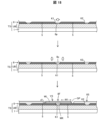
- FIG. 16 is a cross-sectional view showing another method of manufacturing a semiconductor substrate according to this embodiment.
- a buffer section 2 may be provided so as to cover the mask pattern 6.
- a highly reactive AlGaN film can be used for the buffer section 2.
- the upper surface of the buffer section 2 (AlGaN film) includes a growth suppression region SP overlapping with the mask section 5 in plan view, a first seed region 4F overlapping with the first opening K1 in plan view, and a second seed region SP in plan view. It includes a second seed region 4S overlapping with the opening K2.
- a region located above the mask section 5 has low crystallinity and therefore functions as a growth suppressing region SP.
- the regions located above the first and second openings K1 and K2 (above the exposed portion of the base substrate BS) have high crystallinity and therefore function as the first and second seed regions 4F and 4S.
- FIG. 17 is a schematic diagram showing the configuration of a semiconductor substrate manufacturing apparatus according to this embodiment.
- the semiconductor substrate manufacturing apparatus 20 includes a stage 21 on which a template substrate TS including a base substrate BS, a growth suppression region and a seed region is placed, and a nitride semiconductor portion 8 placed on the template substrate TS.
- a raw material supply device 22 that supplies raw materials for growing the semiconductor substrate TS and the semiconductor substrate 10 including the nitride semiconductor portion being grown is irradiated with the first light L1, and a second light emitted from the semiconductor substrate 10.
- the raw material supply device 22 is arranged so that the growth of the first and second nitride semiconductor portions 8F and 8S is stopped before the optical device 23 that receives L2 and the first and second nitride semiconductor portions 8F and 8S meet. and a control device 24 for controlling.
- the control device 24 may be capable of at least one of wired communication and wireless communication with the optical device 23.
- the control device 24 may use the second light L2 to determine the timing for stopping the supply of at least some of the raw materials to the raw material supply device 22.
- a semiconductor substrate manufacturing apparatus 20 is provided with a chamber 25 including a stage SG, a flow channel 27 passing through the chamber 25, and a heating device 26 for heating the chamber 25, and the semiconductor substrate 10 is disposed within the flow channel 27.
- the control device 24 may use the second light L2 to determine the timing at which the heating device 26 stops high-temperature heating (1000 degrees or higher).
- Optical device 23 may be located outside chamber 25.
- the chamber 25 may be provided with a window 28 through which the first light L1 and the second light L2 are transmitted.
- the stage 21 may perform a rotation operation (with the axis in the normal direction of the template substrate TS as the rotation axis).
- the raw material supply device 22 causes the raw material gas to flow horizontally (in a direction parallel to the upper surface of the template substrate) into the flow channel 27, and is exhausted horizontally, but the present invention is not limited thereto.
- the source gas can also be made to flow vertically (in the normal direction of the template substrate TS).
- the control device 24 detects the gap width of the first and second nitride semiconductor parts 8F and 8S in time series using reflectance, which is the ratio of the intensity of the second light L2 to the intensity of the first light L1. Even if the raw material supply device 22 is instructed to stop supplying at least part of the raw material (for example, trimethyl gallium when the nitride semiconductor portion 8 is a GaN crystal) when the gap width reaches a specified value, good. Alternatively, the heating device 26 may be instructed to stop high-temperature heating.
- the control device 24 may be configured to control at least one of the raw material supply device 22 and the heating device 26 by executing a program stored on a built-in memory, a communicable communication device, or an accessible network, for example. , this program, and a recording medium in which this program is stored are also included in this embodiment.
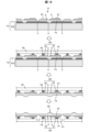
- FIG. 18 is a cross-sectional view showing a method for manufacturing a semiconductor substrate according to Example 1.
- a base portion UB containing a nitride semiconductor is formed on the main substrate 1, and a mask pattern 6 including a plurality of striped mask portions 5 is provided on the base portion UB.
- the mask portion 5 is made of a silicon nitride film with a thickness of 100 nm and a width of 52 ⁇ m, and the m-axis direction of the nitride semiconductor portion 8 is the longitudinal direction.
- the pitch of the stripes in the mask portion 5 is 55 ⁇ m.
- a resist stripe pattern is formed by photolithography on a base substrate BS on which a nitride semiconductor film is formed as a base portion UB.
- a silicon nitride film having a thickness of 100 nm is formed over the entire surface by sputtering.
- the silicon nitride film is patterned by a lift-off method to form a mask pattern 6 (stripe pattern).
- the nitride semiconductor portion 8 is grown on the mask pattern 6 by metal organic chemical vapor deposition (MOCVD) using, for example, trimethyl gallium (TMG) and ammonia (NH 3 ) (ELO method).
- MOCVD metal organic chemical vapor deposition
- an initial growth portion 8p is formed above the base portion UB (seed region) exposed in the openings K1 and K2.
- the growth conditions at this time are referred to as first conditions.
- the growth conditions are adjusted just before the edge of the initial growth part 8p rides on the top surface of the mask part 5 (at the stage where it is in contact with the upper end of the side surface of the mask part 5), or immediately after the edge rides on the top surface of the mask part 5. Start the transition (from the first condition to the second condition).
- Example 1 the first conditions (conditions giving priority to vertical growth) were as follows. Growth temperature (set temperature): 1100° C., growth pressure: 10 kPa, ammonia flow rate: 7.5 slm, trimethyl gallium flow rate: 3 sccm. Further, the second condition (condition giving priority to lateral growth) was set as follows. Growth temperature (set temperature): 1175° C., growth pressure: 10 kPa, ammonia flow rate: 7.5 slm, trimethyl gallium flow rate: 11 sccm.
- the initial growth portion 8p serves as a starting point for the lateral growth of the nitride semiconductor portion 8.
- the initial growth layer 8p can be formed to have a thickness of, for example, 30 nm to 1000 nm, 50 nm to 400 nm, or 70 nm to 350 nm.
- the nitride semiconductor parts 8 grown laterally in opposite directions from two adjacent openings K do not contact (meet) each other on the mask part 5 and have a gap GP. Internal stress can be reduced. Thereby, cracks and defects (dislocations) occurring in the nitride semiconductor portion 8 can be reduced. This effect is particularly effective when the main substrate 1 is a different type of substrate.
- the width of the gap GP can be, for example, 10 ⁇ m or less, 5 ⁇ m or less, 3 ⁇ m or less, or 2 ⁇ m or less.
- the part located above the initial growth part 8p becomes a dislocation inheritance part with many threading dislocations
- the part (wing part) above the mask part 5 has a threading dislocation density lower than that of the dislocation inheritance part. becomes a low-defect part YS where the defect is 1/10 or less.
- a threading dislocation is a dislocation (defect) that extends in the nitride semiconductor portion 8 in its c-axis direction ( ⁇ 0001> direction).
- the threading dislocation density of the low defect portion YS can be, for example, 5 ⁇ 10 6 [pieces/cm 2 ] or less.
- the light emitting part is formed above the low defect part YS (so as to overlap with the low defect part YS in plan view).
- Department can be arranged.
- the ratio (W1/d1) of the size W1 in the a-axis direction to the thickness d1 can be, for example, 2.0 or more. If the method of Example 1 is used, W1/d1 can be set to 1.5 or more, 2.0 or more, 4.0 or more, 5.0 or more, 7.0 or more, or 10.0 or more. It has been found that by setting W1/d1 to 1.5 or more, it becomes easier to divide the nitride semiconductor portion 8 in a subsequent process (for example, a division process in which the cross section becomes an m-plane). Further, the internal stress of the nitride semiconductor portion 8 is reduced, and the warpage of the semiconductor substrate 10 is reduced.
- the nitride semiconductor section 8 (including the initial growth section 8p) shown in FIG. 18 can be a nitride semiconductor crystal (for example, a GaN crystal, an AlGaN crystal, an InGaN crystal, or an InAlGaN crystal).
- the width of the mask portion 5 may be 20 ⁇ m or more, further 30 ⁇ m or more, 50 ⁇ m or more, or 70 ⁇ m or more.
- FIG. 19 is a cross-sectional view showing a method for manufacturing a semiconductor element according to Example 2.
- a step of forming a compound semiconductor section 9 and electrodes D1 and D2 on the semiconductor substrate 10 and a step of forming a nitride semiconductor section 8, a compound semiconductor section 9, and electrodes D1 and D2 are shown.
- the mask portion 5 may be removed by wet etching or the like.
- the nitride semiconductor portion 8 may be an n-type semiconductor crystal.
- the compound semiconductor portion 9 may include a GaN-based semiconductor.
- the compound semiconductor section 9 may include an active section (for example, an active layer such as a quantum well structure) and a p-type semiconductor section, or may include an n-type semiconductor section (for example, a regrowth layer, an n-type contact layer) under the active section. good.
- the active part of the compound semiconductor part 9 includes a light emitting part
- the light emitting part can be arranged above the low defect part YS (so as to overlap with the low defect part YS in plan view). Thereby, luminous efficiency can be increased.
- the electrode D1 located above the low defect portion YS may be an anode, and the electrode D2 may be a cathode.
- the support substrate SK may have a conductive pad in contact with the bonding layer H1 and a conductive pad in contact with the bonding layer H2.
- the bonding layers H1 and H2 may be formed of a solder material.
- the elongated laminate EB may be divided into a plurality of parts (by cutting in the transverse direction); in this case, the nitride semiconductor portion 8 and the compound semiconductor The dividing step may be performed by cleaving the portion 9 (for example, m-plane cleavage in which the cleavage plane is the m-plane).
- end face coating formation of a reflective mirror film
- the stacked body EB is transferred from the base substrate BS to the support substrate SK, but the present invention is not limited to this. It may be transferred from the base substrate BS to a tape or the like one or more times.
- the semiconductor element SD may function as an LED (light emitting diode) element or a semiconductor laser element.
- the support ST may be a submount substrate.
- Embodiment 2 includes electronic equipment (for example, a lighting device, a laser device, a display device, a measuring device, an information processing device, etc.) having the semiconductor element SD.
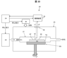
- FIG. 20 is a schematic diagram showing the configuration of a semiconductor substrate manufacturing apparatus according to Example 3.
- the semiconductor substrate manufacturing apparatus of Example 3 includes an imaging device 29 that images the surface (upper surface) of the semiconductor substrate 10 including the template substrate TS and the growing nitride semiconductor portion.
- the imaging device 29 irradiates the semiconductor substrate 10 with first light L1 (illumination light for imaging), and emits second light L2 (light from the mask section 5 and light from the nitride semiconductor section 8) from the semiconductor substrate 10. You may accept it.
- the control device 24 recognizes the gap width of the first and second nitride semiconductor parts 8F and 8S in chronological order using the image sent from the imaging device 29, and when the gap width reaches a specified value, , the raw material supply device 22 may be instructed to stop supplying at least part of the raw material (for example, trimethyl gallium when the nitride semiconductor portion 8 is a GaN crystal). Alternatively, the heating device 26 may be instructed to stop high-temperature heating.
- the gap is recognized by light from the mask section 5. Therefore, the larger the difference between the reflectance of the mask portion 5 and the reflectance of the nitride semiconductor portion 8 with respect to the first light L1, the more clearly the gap can be photographed.
- FIG. 21 is a cross-sectional view showing the method for manufacturing a semiconductor substrate of this embodiment.
- a low defect portion YS wing portion YS located above the growth suppression region SP in the nitride semiconductor portion 8 may be grown so as to be separated from the growth suppression region SP.
- the first and second nitride semiconductor portions 8F and 8F are grown using the first light L1 and the second light L2.
- the width of the gap GP can be controlled to a desired value.
- the seed region 4 (4F/4S) is located below the growth suppression region SP, but the present invention is not limited thereto.
- the seed region 4 may be located flush with the growth suppression region SP, or may be located above it.
Landscapes
- Chemical & Material Sciences (AREA)
- Engineering & Computer Science (AREA)
- Crystallography & Structural Chemistry (AREA)
- Materials Engineering (AREA)
- Metallurgy (AREA)
- Organic Chemistry (AREA)
- Chemical Kinetics & Catalysis (AREA)
- General Chemical & Material Sciences (AREA)
- Inorganic Chemistry (AREA)
- Crystals, And After-Treatments Of Crystals (AREA)
- Recrystallisation Techniques (AREA)
- Chemical Vapour Deposition (AREA)
Priority Applications (3)
| Application Number | Priority Date | Filing Date | Title |
|---|---|---|---|
| KR1020247031997A KR20240160132A (ko) | 2022-03-24 | 2023-03-17 | 반도체 기판의 제조 방법 및 제조 장치 |
| JP2024510120A JPWO2023182194A1 (https=) | 2022-03-24 | 2023-03-17 | |
| DE112023001542.2T DE112023001542T5 (de) | 2022-03-24 | 2023-03-17 | Verfahren und vorrichtung zum herstellen eines halbleitersubstrats |
Applications Claiming Priority (2)
| Application Number | Priority Date | Filing Date | Title |
|---|---|---|---|
| JP2022048788 | 2022-03-24 | ||
| JP2022-048788 | 2022-03-24 |
Publications (1)
| Publication Number | Publication Date |
|---|---|
| WO2023182194A1 true WO2023182194A1 (ja) | 2023-09-28 |
Family
ID=88100807
Family Applications (1)
| Application Number | Title | Priority Date | Filing Date |
|---|---|---|---|
| PCT/JP2023/010518 Ceased WO2023182194A1 (ja) | 2022-03-24 | 2023-03-17 | 半導体基板の製造方法および製造装置 |
Country Status (5)
| Country | Link |
|---|---|
| JP (1) | JPWO2023182194A1 (https=) |
| KR (1) | KR20240160132A (https=) |
| DE (1) | DE112023001542T5 (https=) |
| TW (1) | TWI899553B (https=) |
| WO (1) | WO2023182194A1 (https=) |
Citations (3)
| Publication number | Priority date | Publication date | Assignee | Title |
|---|---|---|---|---|
| JP2011066390A (ja) * | 2009-08-20 | 2011-03-31 | Pawdec:Kk | 半導体素子の製造方法 |
| US20120235115A1 (en) * | 2011-01-24 | 2012-09-20 | Applied Materials, Inc. | Growth of iii-v led stacks using nano masks |
| JP2018520506A (ja) * | 2015-05-15 | 2018-07-26 | オスラム オプト セミコンダクターズ ゲゼルシャフト ミット ベシュレンクテル ハフツングOsram Opto Semiconductors GmbH | 窒素化合物半導体デバイスの製造方法 |
Family Cites Families (1)
| Publication number | Priority date | Publication date | Assignee | Title |
|---|---|---|---|---|
| JP2013251304A (ja) | 2012-05-30 | 2013-12-12 | Furukawa Co Ltd | 積層体および積層体の製造方法 |
-
2023
- 2023-03-17 DE DE112023001542.2T patent/DE112023001542T5/de active Pending
- 2023-03-17 KR KR1020247031997A patent/KR20240160132A/ko active Pending
- 2023-03-17 JP JP2024510120A patent/JPWO2023182194A1/ja active Pending
- 2023-03-17 WO PCT/JP2023/010518 patent/WO2023182194A1/ja not_active Ceased
- 2023-03-21 TW TW112110412A patent/TWI899553B/zh active
Patent Citations (3)
| Publication number | Priority date | Publication date | Assignee | Title |
|---|---|---|---|---|
| JP2011066390A (ja) * | 2009-08-20 | 2011-03-31 | Pawdec:Kk | 半導体素子の製造方法 |
| US20120235115A1 (en) * | 2011-01-24 | 2012-09-20 | Applied Materials, Inc. | Growth of iii-v led stacks using nano masks |
| JP2018520506A (ja) * | 2015-05-15 | 2018-07-26 | オスラム オプト セミコンダクターズ ゲゼルシャフト ミット ベシュレンクテル ハフツングOsram Opto Semiconductors GmbH | 窒素化合物半導体デバイスの製造方法 |
Also Published As
| Publication number | Publication date |
|---|---|
| TW202349464A (zh) | 2023-12-16 |
| JPWO2023182194A1 (https=) | 2023-09-28 |
| KR20240160132A (ko) | 2024-11-08 |
| DE112023001542T5 (de) | 2025-02-20 |
| TWI899553B (zh) | 2025-10-01 |
Similar Documents
| Publication | Publication Date | Title |
|---|---|---|
| EP1508922B1 (en) | Semiconductor light emitting element and production method therefor | |
| JP5635013B2 (ja) | エピタキシャル成長用テンプレート及びその作製方法 | |
| JP5406985B2 (ja) | エピタキシャル成長用テンプレートの作製方法及び窒化物半導体装置 | |
| JP7645319B2 (ja) | 半導体素子 | |
| US9899564B2 (en) | Group III nitride semiconductor and method for producing same | |
| JP2025081377A (ja) | 半導体デバイスの製造方法 | |
| TWI892104B (zh) | 半導體基板 | |
| WO2023182194A1 (ja) | 半導体基板の製造方法および製造装置 | |
| JP7745660B2 (ja) | 半導体基板の製造方法、半導体基板の製造装置 | |
| US6855571B1 (en) | Method of producing GaN-based semiconductor laser device and semiconductor substrate used therefor | |
| JP4232326B2 (ja) | 低欠陥窒化物半導体の成長方法 | |
| JP3555657B2 (ja) | 低欠陥窒化物半導体基板及びその製造方法 | |
| WO2025018196A1 (ja) | 半導体基板の製造方法、半導体基板の製造装置およびテンプレート基板 | |
| JP2003218468A (ja) | 半導体レーザ素子及びその製造方法 | |
| TW202532712A (zh) | 半導體基板、半導體基板之製造方法、半導體裝置之製造方法、半導體裝置、發光元件 | |
| JP2023171128A (ja) | 半導体基板、テンプレート基板、半導体基板の製造方法および製造装置、半導体デバイスの製造方法および製造装置、半導体デバイス | |
| JP2003243776A (ja) | 支持基板の剥離方法 | |
| JP2024083114A (ja) | 半導体基板およびその製造方法 | |
| CN116918032A (zh) | 模板基板及其制造方法、制造装置、半导体基板及其制造方法、制造装置 |
Legal Events
| Date | Code | Title | Description |
|---|---|---|---|
| 121 | Ep: the epo has been informed by wipo that ep was designated in this application |
Ref document number: 23774789 Country of ref document: EP Kind code of ref document: A1 |
|
| ENP | Entry into the national phase |
Ref document number: 2024510120 Country of ref document: JP Kind code of ref document: A |
|
| ENP | Entry into the national phase |
Ref document number: 20247031997 Country of ref document: KR Kind code of ref document: A |
|
| WWE | Wipo information: entry into national phase |
Ref document number: 112023001542 Country of ref document: DE |
|
| WWP | Wipo information: published in national office |
Ref document number: 112023001542 Country of ref document: DE |
|
| 122 | Ep: pct application non-entry in european phase |
Ref document number: 23774789 Country of ref document: EP Kind code of ref document: A1 |