WO2023176960A1 - 回路ユニット、回路ユニットの製造方法、回路ユニットの収容構造、および回路ユニットを備えた装置 - Google Patents
回路ユニット、回路ユニットの製造方法、回路ユニットの収容構造、および回路ユニットを備えた装置 Download PDFInfo
- Publication number
- WO2023176960A1 WO2023176960A1 PCT/JP2023/010585 JP2023010585W WO2023176960A1 WO 2023176960 A1 WO2023176960 A1 WO 2023176960A1 JP 2023010585 W JP2023010585 W JP 2023010585W WO 2023176960 A1 WO2023176960 A1 WO 2023176960A1
- Authority
- WO
- WIPO (PCT)
- Prior art keywords
- connector
- housing
- circuit
- circuit unit
- substrate
- Prior art date
- Legal status (The legal status is an assumption and is not a legal conclusion. Google has not performed a legal analysis and makes no representation as to the accuracy of the status listed.)
- Ceased
Links
Images


Classifications
-
- B—PERFORMING OPERATIONS; TRANSPORTING
- B60—VEHICLES IN GENERAL
- B60Q—ARRANGEMENT OF SIGNALLING OR LIGHTING DEVICES, THE MOUNTING OR SUPPORTING THEREOF OR CIRCUITS THEREFOR, FOR VEHICLES IN GENERAL
- B60Q1/00—Arrangement of optical signalling or lighting devices, the mounting or supporting thereof or circuits therefor
- B60Q1/0088—Details of electrical connections
- B60Q1/0094—Arrangement of electronic circuits separated from the light source, e.g. mounting of housings for starter circuits for discharge lamps
-
- F—MECHANICAL ENGINEERING; LIGHTING; HEATING; WEAPONS; BLASTING
- F21—LIGHTING
- F21S—NON-PORTABLE LIGHTING DEVICES; SYSTEMS THEREOF; VEHICLE LIGHTING DEVICES SPECIALLY ADAPTED FOR VEHICLE EXTERIORS
- F21S41/00—Illuminating devices specially adapted for vehicle exteriors, e.g. headlamps
- F21S41/10—Illuminating devices specially adapted for vehicle exteriors, e.g. headlamps characterised by the light source
- F21S41/19—Attachment of light sources or lamp holders
- F21S41/192—Details of lamp holders, terminals or connectors
-
- F—MECHANICAL ENGINEERING; LIGHTING; HEATING; WEAPONS; BLASTING
- F21—LIGHTING
- F21V—FUNCTIONAL FEATURES OR DETAILS OF LIGHTING DEVICES OR SYSTEMS THEREOF; STRUCTURAL COMBINATIONS OF LIGHTING DEVICES WITH OTHER ARTICLES, NOT OTHERWISE PROVIDED FOR
- F21V15/00—Protecting lighting devices from damage
- F21V15/01—Housings, e.g. material or assembling of housing parts
-
- F—MECHANICAL ENGINEERING; LIGHTING; HEATING; WEAPONS; BLASTING
- F21—LIGHTING
- F21V—FUNCTIONAL FEATURES OR DETAILS OF LIGHTING DEVICES OR SYSTEMS THEREOF; STRUCTURAL COMBINATIONS OF LIGHTING DEVICES WITH OTHER ARTICLES, NOT OTHERWISE PROVIDED FOR
- F21V23/00—Arrangement of electric circuit elements in or on lighting devices
- F21V23/003—Arrangement of electric circuit elements in or on lighting devices the elements being electronics drivers or controllers for operating the light source, e.g. for a LED array
- F21V23/007—Arrangement of electric circuit elements in or on lighting devices the elements being electronics drivers or controllers for operating the light source, e.g. for a LED array enclosed in a casing
-
- F—MECHANICAL ENGINEERING; LIGHTING; HEATING; WEAPONS; BLASTING
- F21—LIGHTING
- F21V—FUNCTIONAL FEATURES OR DETAILS OF LIGHTING DEVICES OR SYSTEMS THEREOF; STRUCTURAL COMBINATIONS OF LIGHTING DEVICES WITH OTHER ARTICLES, NOT OTHERWISE PROVIDED FOR
- F21V23/00—Arrangement of electric circuit elements in or on lighting devices
- F21V23/06—Arrangement of electric circuit elements in or on lighting devices the elements being coupling devices, e.g. connectors
-
- F—MECHANICAL ENGINEERING; LIGHTING; HEATING; WEAPONS; BLASTING
- F21—LIGHTING
- F21V—FUNCTIONAL FEATURES OR DETAILS OF LIGHTING DEVICES OR SYSTEMS THEREOF; STRUCTURAL COMBINATIONS OF LIGHTING DEVICES WITH OTHER ARTICLES, NOT OTHERWISE PROVIDED FOR
- F21V31/00—Gas-tight or water-tight arrangements
- F21V31/005—Sealing arrangements therefor
-
- H—ELECTRICITY
- H01—ELECTRIC ELEMENTS
- H01R—ELECTRICALLY-CONDUCTIVE CONNECTIONS; STRUCTURAL ASSOCIATIONS OF A PLURALITY OF MUTUALLY-INSULATED ELECTRICAL CONNECTING ELEMENTS; COUPLING DEVICES; CURRENT COLLECTORS
- H01R12/00—Structural associations of a plurality of mutually-insulated electrical connecting elements, specially adapted for printed circuits, e.g. printed circuit boards [PCB], flat or ribbon cables, or like generally planar structures, e.g. terminal strips, terminal blocks; Coupling devices specially adapted for printed circuits, flat or ribbon cables, or like generally planar structures; Terminals specially adapted for contact with, or insertion into, printed circuits, flat or ribbon cables, or like generally planar structures
- H01R12/70—Coupling devices
- H01R12/71—Coupling devices for rigid printing circuits or like structures
- H01R12/712—Coupling devices for rigid printing circuits or like structures co-operating with the surface of the printed circuit or with a coupling device exclusively provided on the surface of the printed circuit
-
- H—ELECTRICITY
- H01—ELECTRIC ELEMENTS
- H01R—ELECTRICALLY-CONDUCTIVE CONNECTIONS; STRUCTURAL ASSOCIATIONS OF A PLURALITY OF MUTUALLY-INSULATED ELECTRICAL CONNECTING ELEMENTS; COUPLING DEVICES; CURRENT COLLECTORS
- H01R12/00—Structural associations of a plurality of mutually-insulated electrical connecting elements, specially adapted for printed circuits, e.g. printed circuit boards [PCB], flat or ribbon cables, or like generally planar structures, e.g. terminal strips, terminal blocks; Coupling devices specially adapted for printed circuits, flat or ribbon cables, or like generally planar structures; Terminals specially adapted for contact with, or insertion into, printed circuits, flat or ribbon cables, or like generally planar structures
- H01R12/70—Coupling devices
- H01R12/71—Coupling devices for rigid printing circuits or like structures
- H01R12/72—Coupling devices for rigid printing circuits or like structures coupling with the edge of the rigid printed circuits or like structures
- H01R12/722—Coupling devices for rigid printing circuits or like structures coupling with the edge of the rigid printed circuits or like structures coupling devices mounted on the edge of the printed circuits
- H01R12/724—Coupling devices for rigid printing circuits or like structures coupling with the edge of the rigid printed circuits or like structures coupling devices mounted on the edge of the printed circuits containing contact members forming a right angle
-
- H—ELECTRICITY
- H01—ELECTRIC ELEMENTS
- H01R—ELECTRICALLY-CONDUCTIVE CONNECTIONS; STRUCTURAL ASSOCIATIONS OF A PLURALITY OF MUTUALLY-INSULATED ELECTRICAL CONNECTING ELEMENTS; COUPLING DEVICES; CURRENT COLLECTORS
- H01R13/00—Details of coupling devices of the kinds covered by groups H01R12/70 or H01R24/00 - H01R33/00
- H01R13/46—Bases; Cases
- H01R13/502—Bases; Cases composed of different pieces
- H01R13/512—Bases; Cases composed of different pieces assembled by screw or screws
-
- H—ELECTRICITY
- H01—ELECTRIC ELEMENTS
- H01R—ELECTRICALLY-CONDUCTIVE CONNECTIONS; STRUCTURAL ASSOCIATIONS OF A PLURALITY OF MUTUALLY-INSULATED ELECTRICAL CONNECTING ELEMENTS; COUPLING DEVICES; CURRENT COLLECTORS
- H01R13/00—Details of coupling devices of the kinds covered by groups H01R12/70 or H01R24/00 - H01R33/00
- H01R13/46—Bases; Cases
- H01R13/52—Dustproof, splashproof, drip-proof, waterproof, or flameproof cases
- H01R13/5202—Sealing means between parts of housing or between housing part and a wall, e.g. sealing rings
Definitions
- the present disclosure relates to a circuit unit and a method for manufacturing the same.
- the present disclosure also relates to a structure housing the circuit unit.
- the present disclosure also relates to a device including the circuit unit.
- Patent Document 1 discloses a headlamp as an example of a device mounted on a vehicle as an example of a moving object.
- the headlamp includes a circuit unit including a control circuit for controlling the operation of a light source housed in a housing.
- the board on which the control circuit and the inner connector are mounted is housed in a casing equipped with an outer connector. Electrical connections between the control circuit and the inner and outer connectors are made through soldering.
- the casing is arranged on the outer surface of the housing. Electrical connection between the control circuit and the light source is made through the inner connector. Electrical connections between the control circuit and external devices are made through the outer connector.
- circuit units There is a need to reduce the manufacturing costs of circuit units, structures that house the circuit units, and devices equipped with the circuit units.
- a first embodiment provided by the present disclosure is a circuit unit that includes: A board on which the circuit is mounted, a connector mounted on the board; It is equipped with The connector is a conductive terminal electrically connected to the circuit; a connector housing supporting the conductive terminal; It is equipped with The conductive terminal extends in a direction intersecting the substrate, and has a portion that is in elastic contact with an inner wall of a via hole formed in the substrate, The connector housing extends in a direction intersecting the substrate and has a protrusion fitted into a hole formed in the substrate.
- electrical connection with the circuit is ensured by press-fitting the conductive terminal of the connector into the via hole. Since there is no need to additionally use solder, conductive adhesive, screws, etc., it is possible to simplify manufacturing equipment and process control, reduce environmental impact, and reduce the amount of materials used.
- the manufacturing cost of the circuit unit as well as the manufacturing cost of the structure housing the circuit unit and the device using the circuit unit, can be reduced.
- a second example embodiment provided by the present disclosure is a method for manufacturing a circuit unit, comprising: A step of preparing a board on which the circuit is mounted; preparing a connector including a conductive terminal that is electrically connected to the circuit, a connector housing that supports the conductive terminal, and a convex portion formed on the connector housing; By mounting the connector on the substrate so that the conductive terminal and the convex portion extend in a direction intersecting the substrate, the conductive terminal is brought into elastic contact with the inner wall of a via hole formed in the substrate, and the convex portion extends in a direction intersecting the substrate. a step of fitting the part into a hole formed in the substrate; Contains.
- the third embodiment provided by the present disclosure is a housing structure for a circuit unit, comprising: A housing that divides the space, a circuit unit; It contains The circuit unit is a board housed in the space and on which a circuit is mounted; a connector mounted on the board; It is equipped with The connector is a conductive terminal electrically connected to the circuit; a connector housing supporting the conductive terminal; It is equipped with The conductive terminal is a first portion extending in a first direction intersecting the substrate and in elastic contact with an inner wall of a via hole formed in the substrate; a second portion extending in a second direction and accessible from outside the space through an opening formed in the housing; It has The connector housing has a protrusion extending in the first direction and fitted into a hole formed in the substrate.
- a fourth example aspect provided by the present disclosure is an apparatus comprising: a driven element; A housing that divides the space, a circuit unit comprising a circuit electrically connected to the driven element; It is equipped with The circuit unit is a board accommodated in the space and on which the circuit is mounted; a connector mounted on the board; It is equipped with The connector is a conductive terminal electrically connected to the circuit; a connector housing supporting the conductive terminal; It is equipped with The conductive terminal is a first portion extending in a first direction intersecting the substrate and in elastic contact with an inner wall of a via hole formed in the substrate; a second portion extending in a second direction and accessible from outside the space through an opening formed in the housing; It has The connector housing has a protrusion extending in the first direction and fitted into a hole formed in the substrate.
- a fifth aspect example provided by the present disclosure is a housing structure for a circuit unit, comprising: A housing that divides the space, a circuit unit; It contains The circuit unit is a board housed in the space and on which a circuit is mounted; a connector mounted on the board; a cover covering at least a portion of the circuit and engaging the connector; a fastening member fastening the cover to the housing; It is equipped with
- the connector includes a conductive terminal electrically connected to the circuit, The conductive terminal extends in a first direction along the substrate and has a portion that is accessible from outside the space through an opening formed in the housing, The fastening member fastens the cover to the housing at a position closer to an edge farther from the connector than an edge closer to the connector among both edges of the board in the first direction.
- a sixth aspect provided by the present disclosure is an apparatus, the device comprising: a driven element; A housing that divides the space, a circuit unit comprising a circuit electrically connected to the driven element; It is equipped with The circuit unit is a board accommodated in the space and on which the circuit is mounted; a connector mounted on the board; a cover covering at least a portion of the circuit and engaging the connector; a fastening member fastening the cover to the housing; It is equipped with The connector includes a conductive terminal electrically connected to the circuit, The conductive terminal extends in a first direction along the substrate and has a portion that is accessible from outside the space through an opening formed in the housing, The fastening member fastens the cover to the housing at a position closer to an edge farther from the connector than an edge closer to the connector among both edges of the board in the first direction.
- the stress is transmitted to the cover that engages with the connector, and is transmitted to the housing at the fastening position with the housing that is relatively far from the connector. be let go. This makes it difficult for stress applied to the connector to be locally concentrated on the board.
- a seventh aspect provided by the present disclosure is a circuit unit housing structure, comprising: A housing that divides the space, a circuit unit; It contains The circuit unit is a board housed in the space and on which a circuit is mounted; a connector mounted on the board; a cover covering at least a portion of the circuit; It is equipped with The connector includes a conductive terminal electrically connected to the circuit, The conductive terminal extends in a first direction and has a portion that is accessible from outside the space through an opening formed in the housing; The housing has a guide groove extending in the first direction, The cover has a flange disposed in the guide groove.
- An eighth example aspect provided by the present disclosure is an apparatus comprising: a driven element; A housing that divides the space, a circuit unit comprising a circuit electrically connected to the driven element; It is equipped with The circuit unit is a board accommodated in the space and on which the circuit is mounted; a connector mounted on the board; a cover covering at least a portion of the circuit; It is equipped with The connector includes a conductive terminal electrically connected to the circuit, The conductive terminal extends in a first direction and has a portion that is accessible from outside the space through an opening formed in the housing; The housing has a guide groove extending in the first direction, The cover has a flange disposed in the guide groove.
- the circuit unit is slidable along the guide groove extending in the same direction as the portion of the terminal of the connector that is accessed from the outside of the space. By doing so, the corresponding portion of the terminal can be easily made accessible from outside the space. Since the efficiency of mounting the circuit unit in the housing is increased, it is possible to reduce the manufacturing cost of a structure accommodating the circuit unit and a device equipped with the circuit unit.
- FIG. 1 illustrates a lighting device including a circuit unit according to an embodiment.
- FIG. 1 is a perspective view illustrating the appearance of a circuit unit according to an embodiment.
- FIG. 3 is an exploded perspective view illustrating the configuration of the circuit unit in FIG. 2.
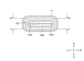
- FIG. 2 illustrates an example of the external appearance of the connector viewed from the direction of arrow IV in FIG. 1.
- a cross section taken along line VV in FIG. 4 in the direction of the arrow is illustrated.
- a cross section taken along line VI-VI in FIG. 4 in the direction of the arrow is illustrated.
- a cross section taken along the line VII-VII in FIG. 6 in the direction of the arrow is illustrated.
- a cross section taken along line VIII-VIII in FIG. 6 in the direction of the arrow is illustrated.
- a lighting device including a circuit unit according to another embodiment is illustrated.
- arrow F indicates the forward direction of the illustrated structure.
- Arrow B indicates the rearward direction of the illustrated structure.
- Arrow U indicates the upward direction of the illustrated structure.
- Arrow D indicates the downward direction of the illustrated structure.
- Arrow R indicates the right direction of the illustrated structure.
- Arrow L indicates the left direction of the illustrated structure.
- front-back direction used in this specification means a direction along the above-mentioned front direction and rear direction.
- vertical direction used in this specification means a direction along the above-mentioned upward and downward directions.
- left-right direction used in this specification means a direction along the above-mentioned left direction and right direction.
- extending in the front-back direction includes extending at an angle with respect to the front-back direction, and means extending at an angle closer to the front-back direction than the up-down direction and the left-right direction.
- extending in the vertical direction includes extending at an angle with respect to the up-down direction, and means extending at an inclination closer to the up-down direction than the front-back direction and the left-right direction.
- extending in the left-right direction includes extending at an angle with respect to the left-right direction, and means extending at an inclination closer to the left-right direction than the front-back direction and the up-down direction.
- FIG. 1 schematically illustrates the configuration of a lighting device 10 according to an embodiment.
- the lighting device 10 according to this example is configured to be mounted on a vehicle. There is no limitation on the number of wheels that the vehicle has.
- the vehicle is an example of a moving object.
- the lighting device 10 includes a housing 11 and a transparent cover 12.
- the housing 11 and the light-transmitting cover define a lamp chamber 13.
- the light chamber 13 is an example of a space partitioned by a housing.
- the lighting device 10 includes a lamp unit 14.
- the lamp unit 14 includes a light source 141.
- the light source 141 is configured to emit visible light.
- the light source 141 may be a lamp light source or a semiconductor light emitting device. Examples of semiconductor light emitting devices include light emitting diodes, laser diodes, electroluminescent devices, and the like.
- the light source 141 is configured to emit light including wavelengths in the visible light range. The light emitted from the light source 141 passes through the transparent cover 12 and heads toward the outside of the vehicle.
- the lighting device 10 includes a circuit unit 15.
- the circuit unit 15 includes a board 151 and a connector 152.
- the board 151 is housed within the lamp chamber 13.
- Connector 152 is mounted on board 151.
- the configuration of the circuit unit 15 will be described in detail with reference to FIGS. 2 and 3.
- the circuit unit 15 includes an upper cover 153 and a lower cover 154.
- the upper cover 153 and the lower cover 154 are fastened together by a fastening member 156 so as to sandwich the substrate 151 therebetween.
- the upper cover 153 and the lower cover 154 cover at least a portion of the circuit 155 mounted on the board 151.
- Each of the upper cover 153 and the lower cover 154 is preferably made of metal from the viewpoint of radio wave shielding function for the circuit 155.
- the lower cover 154 may be omitted.
- the circuit unit 15 includes an internal connector 157.
- the circuit 155 is electrically connected to the light source 141 of the lamp unit 14 via an internal connector 157.
- Circuit 155 includes circuit elements for driving light source 141.
- Light source 141 is an example of a driven element.
- FIG. 4 illustrates the configuration seen from the direction of arrow IV in FIG. In the figure, illustration of the back surface 111 is omitted.
- the connector 152 includes a plurality of terminals 152a and a connector housing 152b.
- the connector housing 152b is made of an electrically insulating material.
- the plurality of connector terminals 152a are supported by the connector housing 152b while ensuring mutual electrical insulation.
- the plurality of terminals 152a are arranged in the left-right direction.
- each of the plurality of terminals 152a is made of a conductive material and is electrically connected to the circuit 155.
- all the terminals 152a may be formed of a conductive material and may not be electrically connected to the circuit 155.
- the plurality of terminals 152a may include dummy terminals.
- FIG. 5 schematically illustrates a cross section taken along the line VV in FIG. 4 in the direction of the arrow.
- each terminal 152a has a first portion 152a1.
- the first portion 152a1 extends in the vertical direction.
- the vertical direction is an example of a direction intersecting the substrate 151.
- each via hole 151a has an inner wall covered with a conductive material.
- each via hole 151a is a through hole.
- at least one of the plurality of via holes 151a may be a bottomed hole.
- each terminal 152a is associated with one of the plurality of via holes 151a, and is inserted into the one via hole 151a.
- Each terminal 152a is configured as a press-fit terminal. That is, the first portion 152a1 has a width larger than the width of the corresponding via hole 151a in an initial state, and includes an elastically deformable portion. Therefore, the terminal 152a is inserted into the via hole 151a through press fitting.
- press fitting used in this specification means an operation of inserting a member having a width dimension greater than the width of the hole or recess into a hole or recess.
- the first portion 152a1 is in elastic contact with the inner wall of the via hole 151a. This ensures electrical connection between the terminal 152a and the circuit 155 via the conductive material covering the inner wall of the via hole 151a.
- Each terminal 152a has a second portion 152a2.
- the second portion 152a2 extends in the front-rear direction.
- the front-back direction is an example of a direction along the substrate 151.
- the second portion 152a2 is a portion that is accessible from the outside of the lamp chamber 13 through the opening 112 formed in the housing 11.
- the second portion 152a2 is a portion used for connection with a terminal of a mating connector (not shown).
- the mating connector may be electrically connected to a device located outside the lighting device 10.
- the mating connector may be a jumper connection connector that selectively connects specific terminals to each other.
- the connector housing 152b has a plurality of protrusions 152b1.
- Each convex portion 152b1 extends in the vertical direction. That is, each convex portion 152b1 extends in a direction intersecting the substrate 151. In this example, four convex portions 152b1 are provided. However, one of the protrusions 152b1 may be omitted.
- each fitting hole 151b is a through hole.
- at least one of the plurality of fitting holes 151b may be a bottomed hole.
- each protrusion 152b1 is associated with one of the plurality of fitting holes 151b, and is press-fitted into the one fitting hole 151b.
- the circuit unit 15 can be manufactured by the procedure illustrated below.
- a substrate 151 in which a plurality of via holes 151a and a plurality of fitting holes 151b are formed is prepared.
- the circuit 155 may be mounted on the substrate 151 at this point, or may be mounted in a later process.
- the connector 152 is mounted on the board 151. Specifically, the connector 152 is mounted on the substrate 151 such that the first portion 152a1 of each terminal 152a and each convex portion 152b1 extend in a direction intersecting the substrate 151. As a result, each first portion 152a1 is press-fitted into the corresponding via hole 151a, and each convex portion 152b1 is press-fitted into the corresponding fitting hole 151b at the same time.
- the connector 152 is fixed to the substrate 151 and electrically connected to the circuit 155 by elastic contact of the first portion 152a1 with the inner wall of the via hole 151a and by fitting the convex portion 152b1 into the fitting hole 151b.
- electrical connection with the circuit 155 is ensured by press-fitting the terminal 152a of the connector 152 into the via hole 151a. Since there is no need to additionally use solder, conductive adhesive, screws, etc., it is possible to simplify manufacturing equipment and process control, reduce environmental impact, and reduce the amount of materials used.
- the manufacturing cost of the circuit unit 15 and, by extension, the manufacturing cost of the lighting device 10 including the circuit unit 15 can be reduced.
- the convex portion 152b1 that is press-fitted into the fitting hole 151b formed in the substrate 151 has a circular cross-sectional shape.
- the cross-sectional shape may be any polygonal shape as long as it can be press-fitted into the fitting hole 151b.
- a press-fit terminal having a simple configuration is used as the terminal 152a of the connector 152. This fact can also contribute to reducing the manufacturing cost of the circuit unit 15.
- the configuration of the first portion 152a1 of the terminal 152a press-fitted into the via hole 151a may be changed as appropriate, as long as the electrical connection with the circuit 155 can be ensured by making elastic contact with the inner wall of the via hole 151a.
- the first portion 152a1 may be configured to include a shaft body extending in a direction intersecting the substrate 151, and a movable body biased radially outward of the shaft body by a spring.
- the board 151 of the circuit unit 15 is housed in the housing 11, and the connector 152 is inserted into the opening 112 from the inside of the housing 11. , the circuit unit 15 is mounted on the lighting device 10.
- the lighting device 10 includes a sealing member 16.
- the sealing member 16 is made of an elastic material. The material and shape of the sealing member 16 are determined so as to ensure waterproofness and dustproofness for the lamp chamber 13. Examples of the sealing member 16 include a gasket and an O-ring.
- the sealing member 16 is attached to the connector 152 so as to be disposed between the connector housing 152b and the opening 112.
- the electrical connection between the light source 141 and the circuit unit 15 is made via the internal connector 157.
- the orientation of the conductive terminals included in the internal connector 157 can be determined arbitrarily, it is preferable that the direction corresponds to the direction in which the second portion 152a2 of the terminal 152a in the connector 152 extends.
- the direction in which the connector housing 152b is inserted into the opening 112 of the housing 11 coincides with the direction in which the connector electrically connected to the light source 141 is fitted into the internal connector 157. .
- This improves assembly workability, which can contribute to reducing the manufacturing cost of the lighting device 10.
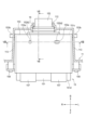
- FIG. 6 illustrates a cross section taken along the line VI-VI in FIG. 4 in the direction of the arrow.
- the connector housing 152b of the connector 152 has a pair of protrusions 152b2.
- Each convex portion 152b2 extends in the vertical direction.
- a pair of holes 153a are formed in the upper cover 153.
- each protrusion 152b2 engages with one of the corresponding pair of holes 153a.
- the circuit unit 15 includes a fastening member 158.
- the fastening member 158 fixes the circuit unit 15 to the housing 11 by fastening the upper cover 153 to the housing 11.
- the fastening member 158 connects the upper cover 153 to the housing 11 at a position closer to the front edge 151d, which is farther from the connector 152 than the rear edge 151c, which is closer to the connector 152, of both edges in the front-rear direction of the board 151. has concluded.
- the convex portion 152b2 engages with the upper cover 153 at a position closer to the rear edge 151c, which is closer to the connector 152, than the front edge 151d, which is farther from the connector 152, of both edges in the front-rear direction of the board 151. It matches.
- the stress applied to the connector 152 can be released to the upper cover 153 more quickly, so that the local concentration of the stress on the substrate 151 can be easily alleviated.
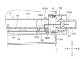
- FIG. 7 illustrates a cross section taken along line VII-VII in FIG. 6 in the direction of the arrow.
- FIG. 8 illustrates a cross section taken along line VIII-VIII in FIG. 6 in the direction of the arrow.
- the housing 11 has a pair of guide walls 113.
- the pair of guide walls 113 face each other in the left-right direction.
- a guide groove 114 is formed in each guide wall 113.
- the guide groove 114 extends in the front-rear direction. That is, the guide groove 114 extends in the same direction as the direction in which the second portion 152a2 of the terminal 152a of the connector 152 extends.
- the upper cover 153 of the circuit unit 15 has a plurality of collar portions 153b.
- Each collar portion 153b extends in the left-right direction.
- the circuit unit 15 is attached to the housing 11 by being inserted between the pair of guide walls 113 from the front. As illustrated in FIG. 6, the distance between the pair of guide walls 113 in the left-right direction narrows as it approaches the back surface 111. Thereby, the connector 152 is guided to the opening 112 while being positioned in the left-right direction.
- Each guide groove 114 has a pair of inner walls 114a facing each other in the vertical direction. Thereby, the connector 152 is guided to the opening 112 while being positioned in the vertical direction.
- the terminal 152a of the connector 152 can be easily connected to the lamp chamber. It can be made accessible from outside of 13. Since the efficiency of mounting the circuit unit 15 on the housing 11 is increased, the manufacturing cost of the lighting device 10 can be reduced.
- a gap is formed in the vertical direction between the flange 153b of the upper cover 153 and the inner wall 114a of the guide groove 114.
- the up-down direction in this case is an example of a direction intersecting the direction in which the guide groove 114 extends.
- the width of the guide groove 114 in the vertical direction becomes narrower as it approaches the opening 112.
- the pair of inner walls 114a are both formed as inclined surfaces.
- the angle formed by both inclined surfaces may be, for example, 3° to 5°. According to such a configuration, the positioning function of the connector 152 in the above-described vertical direction can be enhanced.
- one of the inner walls 114a may be a flat surface.
- the pair of inner walls 114a face each other in the vertical direction (vertical direction) as in this example, it is preferable that the lower inner wall 114a is a flat surface. According to such a configuration, after the circuit unit 15 is attached to the housing 11, the upper cover 153 can be supported by the lower inner wall 114a, increasing the stability of the structure.
- the pair of protrusions 152b2 formed on the connector housing 152b engage with the upper cover 153 through the pair of holes 153a.
- force can be easily transmitted to the connector 152.
- This configuration is advantageous when the resistance to insertion of the connector 152 is relatively high (eg, when the sealing member 16 is disposed between the connector housing 152b and the opening 112).
- the convex portion 152b2 for releasing external force applied to the connector 152 from the outside to the upper cover 153 is also used to improve the workability of inserting the connector 152 into the opening 112.
- these two functions may be realized by independent engagement structures between the connector 152 and the top cover 153.
- the fastening direction of the upper cover 153 to the housing 11 by the fastening member 158 is arbitrary, it is preferable that the fastening is done along the direction in which the guide groove 114 extends, as illustrated in FIG.
- the direction in which the connector housing 152b is inserted into the opening 112 of the housing 11 coincides with the direction in which the upper cover 153 is fastened to the housing. This increases the efficiency of mounting the circuit unit 15 on the housing 11, which can contribute to reducing the manufacturing cost of the lighting device 10.
- the first portion 152a1 of the terminal 152a in the connector 152 extends in a direction along the substrate 151.
- the attitude of the board 151 and the attitude of the connector 152 can have a relationship as illustrated in FIG. 9 .
- both the first portion 152a1 and the second portion 152a2 of the terminal 152a extend in a direction intersecting the substrate 151.
- the connector 152 of the circuit unit 15 is inserted into the opening 112 formed in the back surface 111 of the housing 11.
- the position of the opening 112 can be determined as appropriate depending on the specifications of the lighting device 10.
- the relationship between the posture of the board 151 and the posture of the connector 152 can also be determined as appropriate.
- the circuit 155 mounted on the board 151 of the circuit unit 15 is electrically connected to the light source 141 of the lamp unit 14.
- the circuit 155 includes a device that dissipates heat generated from the light source 141, a device that changes the direction of light emitted from the light source 141, a device that changes the light distribution pattern formed by the light emitted from the light source 141, etc. may be electrically connected to. These devices are also examples of driven elements.
- the circuit unit 15 does not need to be mounted on the lighting device 10.
- the circuit 155 may control the operation of a sensor housed in a space defined by the housing 11. That is, the circuit unit 15 can be installed in a sensor device for acquiring predetermined information.
- sensors include a LiDAR (Light Detection and Ranging) sensor, a camera, a millimeter wave radar, an ultrasonic sensor, a temperature sensor, and the like. These sensors are also examples of driven elements.
- the lighting device 10 and the sensor device described above may be mounted on a moving object other than a vehicle.
- Examples of other moving objects include aircraft, flying objects, ships, and the like.
- the mobile object may not require a driver.
- the lighting device 10 and the sensor device described above do not need to be mounted on a moving body.
- the lighting device 10 and the sensor device described above can also be applied to a system that is installed in a house, facility, transportation infrastructure, etc. and operates in response to an object that enters a specific area.
- the lighting device 10 can also be applied to a device that temporarily displays predetermined figures, characters, signs, etc. on a specific road surface or wall surface.
- the circuit unit 15 does not need to be electrically connected to a specific driven element.
- the housing 11 having the opening 112 can function as a housing structure for the circuit unit 15. According to the configuration of the present disclosure, the manufacturing cost of the accommodation structure can also be reduced.
- Japanese Patent Application No. 2022-044215 filed on March 18, 2022
- Japanese Patent Application No. 2022-044216 filed on March 18, 2022
- the contents of Japanese Patent Application No. 2022-044217 filed on March 18, 2022 are incorporated.
Landscapes
- Engineering & Computer Science (AREA)
- General Engineering & Computer Science (AREA)
- Mechanical Engineering (AREA)
- Microelectronics & Electronic Packaging (AREA)
- Arrangement Of Elements, Cooling, Sealing, Or The Like Of Lighting Devices (AREA)
Priority Applications (4)
| Application Number | Priority Date | Filing Date | Title |
|---|---|---|---|
| EP23770912.6A EP4495478A4 (en) | 2022-03-18 | 2023-03-17 | CIRCUIT UNIT, METHOD FOR PRODUCING CIRCUIT UNIT, CIRCUIT UNIT RECEIVING STRUCTURE, AND DEVICE COMPRISING CIRCUIT UNIT |
| CN202380028330.9A CN118900968A (zh) | 2022-03-18 | 2023-03-17 | 电路单元、电路单元的制造方法、电路单元的容纳结构以及具备电路单元的装置 |
| JP2024508276A JPWO2023176960A1 (https=) | 2022-03-18 | 2023-03-17 | |
| US18/847,893 US20250222854A1 (en) | 2022-03-18 | 2023-03-17 | Circuit unit, method of manufacturing the circuit unit, housing structure for the circuit unit, and device provided with the circuit unit |
Applications Claiming Priority (6)
| Application Number | Priority Date | Filing Date | Title |
|---|---|---|---|
| JP2022-044215 | 2022-03-18 | ||
| JP2022-044217 | 2022-03-18 | ||
| JP2022044217 | 2022-03-18 | ||
| JP2022-044216 | 2022-03-18 | ||
| JP2022044215 | 2022-03-18 | ||
| JP2022044216 | 2022-03-18 |
Publications (1)
| Publication Number | Publication Date |
|---|---|
| WO2023176960A1 true WO2023176960A1 (ja) | 2023-09-21 |
Family
ID=88023381
Family Applications (1)
| Application Number | Title | Priority Date | Filing Date |
|---|---|---|---|
| PCT/JP2023/010585 Ceased WO2023176960A1 (ja) | 2022-03-18 | 2023-03-17 | 回路ユニット、回路ユニットの製造方法、回路ユニットの収容構造、および回路ユニットを備えた装置 |
Country Status (4)
| Country | Link |
|---|---|
| US (1) | US20250222854A1 (https=) |
| EP (1) | EP4495478A4 (https=) |
| JP (1) | JPWO2023176960A1 (https=) |
| WO (1) | WO2023176960A1 (https=) |
Cited By (1)
| Publication number | Priority date | Publication date | Assignee | Title |
|---|---|---|---|---|
| WO2025205138A1 (ja) * | 2024-03-29 | 2025-10-02 | 株式会社小糸製作所 | 電子ユニット及び車両用灯具 |
Citations (11)
| Publication number | Priority date | Publication date | Assignee | Title |
|---|---|---|---|---|
| JP2005129275A (ja) * | 2003-10-21 | 2005-05-19 | Fujitsu Ten Ltd | コネクタ固定構造 |
| JP2008166180A (ja) * | 2006-12-28 | 2008-07-17 | Keihin Corp | 電子回路基板とコネクタの接続構造 |
| JP2009200115A (ja) * | 2008-02-19 | 2009-09-03 | Keihin Corp | 電子基板の保持構造 |
| JP2014082147A (ja) | 2012-10-18 | 2014-05-08 | Koito Mfg Co Ltd | 電子ユニット |
| JP2014211989A (ja) * | 2013-04-17 | 2014-11-13 | 株式会社デンソー | Led駆動装置及びその取付構造 |
| JP2015230834A (ja) * | 2014-06-05 | 2015-12-21 | 株式会社小糸製作所 | 車両用灯具 |
| WO2017163573A1 (ja) * | 2016-03-22 | 2017-09-28 | 日立オートモティブシステムズ株式会社 | 電子制御装置 |
| JP2019016514A (ja) * | 2017-07-06 | 2019-01-31 | 株式会社デンソーテン | コネクタの取付構造およびコネクタシールド |
| JP2022044217A (ja) | 2020-09-07 | 2022-03-17 | 日本信号株式会社 | リレー制御装置 |
| JP2022044215A (ja) | 2020-09-07 | 2022-03-17 | ミツミ電機株式会社 | 電源用半導体集積回路 |
| JP2022044216A (ja) | 2020-09-07 | 2022-03-17 | インタープロテイン株式会社 | 新型コロナウイルス感染症(covid-19)の予防または治療剤および医薬組成物 |
Family Cites Families (2)
| Publication number | Priority date | Publication date | Assignee | Title |
|---|---|---|---|---|
| WO2001023803A1 (en) * | 1999-09-30 | 2001-04-05 | Matsushita Electric Works, Ltd. | Illumination device |
| FR3083179B1 (fr) * | 2018-06-29 | 2021-05-07 | Valeo Vision | Dispositif lumineux pour vehicule automobile |
-
2023
- 2023-03-17 WO PCT/JP2023/010585 patent/WO2023176960A1/ja not_active Ceased
- 2023-03-17 US US18/847,893 patent/US20250222854A1/en active Pending
- 2023-03-17 JP JP2024508276A patent/JPWO2023176960A1/ja active Pending
- 2023-03-17 EP EP23770912.6A patent/EP4495478A4/en active Pending
Patent Citations (11)
| Publication number | Priority date | Publication date | Assignee | Title |
|---|---|---|---|---|
| JP2005129275A (ja) * | 2003-10-21 | 2005-05-19 | Fujitsu Ten Ltd | コネクタ固定構造 |
| JP2008166180A (ja) * | 2006-12-28 | 2008-07-17 | Keihin Corp | 電子回路基板とコネクタの接続構造 |
| JP2009200115A (ja) * | 2008-02-19 | 2009-09-03 | Keihin Corp | 電子基板の保持構造 |
| JP2014082147A (ja) | 2012-10-18 | 2014-05-08 | Koito Mfg Co Ltd | 電子ユニット |
| JP2014211989A (ja) * | 2013-04-17 | 2014-11-13 | 株式会社デンソー | Led駆動装置及びその取付構造 |
| JP2015230834A (ja) * | 2014-06-05 | 2015-12-21 | 株式会社小糸製作所 | 車両用灯具 |
| WO2017163573A1 (ja) * | 2016-03-22 | 2017-09-28 | 日立オートモティブシステムズ株式会社 | 電子制御装置 |
| JP2019016514A (ja) * | 2017-07-06 | 2019-01-31 | 株式会社デンソーテン | コネクタの取付構造およびコネクタシールド |
| JP2022044217A (ja) | 2020-09-07 | 2022-03-17 | 日本信号株式会社 | リレー制御装置 |
| JP2022044215A (ja) | 2020-09-07 | 2022-03-17 | ミツミ電機株式会社 | 電源用半導体集積回路 |
| JP2022044216A (ja) | 2020-09-07 | 2022-03-17 | インタープロテイン株式会社 | 新型コロナウイルス感染症(covid-19)の予防または治療剤および医薬組成物 |
Non-Patent Citations (1)
| Title |
|---|
| See also references of EP4495478A4 |
Cited By (1)
| Publication number | Priority date | Publication date | Assignee | Title |
|---|---|---|---|---|
| WO2025205138A1 (ja) * | 2024-03-29 | 2025-10-02 | 株式会社小糸製作所 | 電子ユニット及び車両用灯具 |
Also Published As
| Publication number | Publication date |
|---|---|
| JPWO2023176960A1 (https=) | 2023-09-21 |
| EP4495478A4 (en) | 2025-07-16 |
| EP4495478A1 (en) | 2025-01-22 |
| US20250222854A1 (en) | 2025-07-10 |
Similar Documents
| Publication | Publication Date | Title |
|---|---|---|
| US10836320B2 (en) | Light module, light assembly and rear view device for a vehicle | |
| US7701144B2 (en) | Vehicular lamp | |
| EP3527877A1 (en) | Light source unit for lighting tool for vehicle and lighting tool for vehicle | |
| US10036546B2 (en) | Lamp and manufacturing method thereof | |
| WO2023176960A1 (ja) | 回路ユニット、回路ユニットの製造方法、回路ユニットの収容構造、および回路ユニットを備えた装置 | |
| KR102417588B1 (ko) | 자동차용 조명 수단을 위한 지지체 | |
| US20180347780A1 (en) | Dual printed circuit board | |
| KR102262690B1 (ko) | 특정 사전 조립 모듈을 갖는 자동차의 광학 감지 장치용 발광 장치, 광학 감지 장치 및 자동차 | |
| JP2020145120A (ja) | 車輌用灯具 | |
| JP2017228460A (ja) | 電気接続用端子構造 | |
| CN118900968A (zh) | 电路单元、电路单元的制造方法、电路单元的容纳结构以及具备电路单元的装置 | |
| JP5580170B2 (ja) | 車両用灯具 | |
| JP6889592B2 (ja) | 灯具 | |
| KR102512377B1 (ko) | 엘이디 드라이버 모듈 및 이를 포함하는 차량 | |
| CN104949028A (zh) | 车辆用灯具 | |
| JP2005175137A (ja) | フレキシブル基板のターミナル構造 | |
| US11149928B2 (en) | Lamp with connection terminal and coupling member for vehicle and method for assembling the same | |
| JP6126836B2 (ja) | 電気接続構造および車両用灯具 | |
| JP6226699B2 (ja) | 車両用灯具 | |
| JP7121574B2 (ja) | 灯具 | |
| JP4597082B2 (ja) | 車両用燈体 | |
| CN117157485A (zh) | 照明装置、制造照明装置的方法以及汽车前照灯 | |
| US10969441B2 (en) | Illumination apparatus and headlamp | |
| KR102322468B1 (ko) | 차량용 램프 및 차량용 램프를 조립하는 방법 | |
| JP2012230772A (ja) | 車両用灯具用反射ユニットおよび車両用灯具 |
Legal Events
| Date | Code | Title | Description |
|---|---|---|---|
| 121 | Ep: the epo has been informed by wipo that ep was designated in this application |
Ref document number: 23770912 Country of ref document: EP Kind code of ref document: A1 |
|
| WWE | Wipo information: entry into national phase |
Ref document number: 2024508276 Country of ref document: JP |
|
| WWE | Wipo information: entry into national phase |
Ref document number: 18847893 Country of ref document: US |
|
| WWE | Wipo information: entry into national phase |
Ref document number: 202380028330.9 Country of ref document: CN |
|
| WWE | Wipo information: entry into national phase |
Ref document number: 2023770912 Country of ref document: EP |
|
| NENP | Non-entry into the national phase |
Ref country code: DE |
|
| ENP | Entry into the national phase |
Ref document number: 2023770912 Country of ref document: EP Effective date: 20241018 |
|
| WWP | Wipo information: published in national office |
Ref document number: 18847893 Country of ref document: US |