WO2023149331A1 - 光子数識別装置及び方法 - Google Patents
光子数識別装置及び方法 Download PDFInfo
- Publication number
- WO2023149331A1 WO2023149331A1 PCT/JP2023/002423 JP2023002423W WO2023149331A1 WO 2023149331 A1 WO2023149331 A1 WO 2023149331A1 JP 2023002423 W JP2023002423 W JP 2023002423W WO 2023149331 A1 WO2023149331 A1 WO 2023149331A1
- Authority
- WO
- WIPO (PCT)
- Prior art keywords
- unit
- light receiving
- photon number
- electrical signal
- light
- Prior art date
- Legal status (The legal status is an assumption and is not a legal conclusion. Google has not performed a legal analysis and makes no representation as to the accuracy of the status listed.)
- Ceased
Links
Images




Classifications
-
- G—PHYSICS
- G01—MEASURING; TESTING
- G01J—MEASUREMENT OF INTENSITY, VELOCITY, SPECTRAL CONTENT, POLARISATION, PHASE OR PULSE CHARACTERISTICS OF INFRARED, VISIBLE OR ULTRAVIOLET LIGHT; COLORIMETRY; RADIATION PYROMETRY
- G01J1/00—Photometry, e.g. photographic exposure meter
- G01J1/02—Details
-
- G—PHYSICS
- G01—MEASURING; TESTING
- G01J—MEASUREMENT OF INTENSITY, VELOCITY, SPECTRAL CONTENT, POLARISATION, PHASE OR PULSE CHARACTERISTICS OF INFRARED, VISIBLE OR ULTRAVIOLET LIGHT; COLORIMETRY; RADIATION PYROMETRY
- G01J11/00—Measuring the characteristics of individual optical pulses or of optical pulse trains
-
- H—ELECTRICITY
- H10—SEMICONDUCTOR DEVICES; ELECTRIC SOLID-STATE DEVICES NOT OTHERWISE PROVIDED FOR
- H10N—ELECTRIC SOLID-STATE DEVICES NOT OTHERWISE PROVIDED FOR
- H10N60/00—Superconducting devices
Definitions
- the present disclosure relates to a photon number identification device and method.
- a photon number discriminator which can measure the number of photons in incident light, is expected to be used in various fields such as quantum optics, extremely weak light measurement, and optical sensing as an optical power meter to accurately measure the power of an optical signal. ing.
- special quantum states non-Gaussian quantum states
- a pseudo photon number discriminator has been used in the past by temporally or spatially multiplexing single photon detectors that can discriminate only the presence or absence of photons. was attempted to construct.
- photodetection sensors with such a single-pixel photon number discrimination performance include a superconducting transition edge sensor (TES) and a superconducting nanostrip photon detector (SNSPD). )It has been known. Note that the “nanostrip” in the name of SNSPD is sometimes written or called “nanowire”, but the term “nanostrip” used in the present disclosure includes “nanowire”, and both are equivalent. shall be
- TES measures the number of photons from the temperature rise when photons are incident on a metal thin film cooled to near the superconducting transition temperature, and has achieved a detection efficiency of nearly 100%. can be identified.
- TES requires a special device called a superconducting quantum interferometer to read out photon signals, and due to its limited response speed, the time resolution of TES is several nanoseconds or more even with the fastest device. end up
- the operating temperature of the metal thin film used for TES is on the order of 100 mK, and large-sized refrigerators such as adiabatic demagnetization refrigerators and dilution refrigerators are required, which limits the environment in which the entire system can be installed. put away.
- SNSPDs are expected to be used in various fields such as the above-mentioned quantum information communication, quantum optics, and extremely weak light sensors as photon detectors capable of high sensitivity, low noise, and high speed operation.
- a wire-shaped light receiving portion called a nanostrip arranged in a predetermined light receiving surface area is used as a light detecting element.
- the light-receiving portion is formed of ultrafine wires such as niobium nitride (NbN), titanium niobium nitride (NbTiN), tungsten silicide (WSi), molybdenum silicide (MoSi), etc., and functions as a photodetector in a superconducting state.
- wires such as niobium nitride (NbN), titanium niobium nitride (NbTiN), tungsten silicide (WSi), molybdenum silicide (MoSi), etc.
- Non-Patent Documents 1 to 3 The time resolution of such an SNSPD type photon number discriminator is on the order of 10 ps, and it has a response characteristic about 100 times faster than that of the TES described above.
- the light-receiving part used in the SNSPD can be operated by, for example, a small pulse tube refrigerator or a Gifford-McMahon (GM) refrigerator, thereby reducing the size of the entire system and saving space. have the great advantage of obtaining
- the portion of the signal waveform measured by the SNSPD that contains information on the number of photons is only a portion of about 100 ps at the rising edge.
- a low-speed measurement system equipped with an instrument there is a problem that accurate photon number discrimination cannot be performed.
- Complex processing using a high-speed, special measurement system for example, a combination of a high-speed AD converter and a high-speed circuit such as FPGA or ASIC) is indispensable, and the cost tends to increase.
- the present disclosure has been made in view of such circumstances, and is capable of reducing the influence of noise while maintaining the excellent optical response characteristics (photodetection characteristics) of SNSPD, and providing a low-speed, narrow band. Even if the measurement system is used, it is possible to achieve accurate and simple photon number discrimination, and by these, a photon number discrimination device and method that are excellent in economic efficiency, operability, and versatility intended to provide
- An example of a photon number identification device is a device for identifying the number of photons contained in an optical signal from a light source, and is a single-pixel nanostrip arranged on a predetermined light receiving surface area. and a photodetector that, in a superconducting state, generates an electrical signal corresponding to the optical signal; a photodetector unit including a vibration imparting unit having electrical circuit characteristics to be imparted to the electrical signal; a power supply unit that supplies a bias current to the photodetector unit; an amplifier unit that amplifies the electrical signal; and the photodetector unit. and a cryostat that accommodates the amplifying section and operates at a temperature at which the light receiving section exhibits a superconducting state.
- a configuration equivalent to the photodetector element of the SNSPD that is cooled by the cryostat so as to be in a superconducting state can be adopted as the light receiving section.
- an amplitude vibration component corresponding to the number of photons that is, a vibration characteristic component
- the electrical signal output from the photodetector is superimposed with a plurality of components having different amplitude oscillations depending on the number of photons, and lasts, for example, about 10 ns or more. Show the waveform.
- the high-speed signal processing of the rising portion required in the SNSPD becomes unnecessary, and based on the number of amplitude oscillation components with different intensities in the electrical signal from the photodetector or its amplified signal waveform, the number of photons Identification and counting are possible.
- the frequency of the amplitude vibration component is expressed by the following formula (1);
- the light detection unit in the present disclosure can be regarded as an equivalent circuit in which both the light receiving unit and the vibration applying unit have predetermined inductances Ls and Lc and predetermined capacitances (parasitic capacitances) Cs and Cc as internal elements like electrical elements. Therefore, the connection between the two generates the resonance frequency represented by the above formula (1), and with such a simple element structure, an amplitude vibration component is added to the electrical signal generated by the light receiving section, and noise can be suppressed as much as possible.
- the vibration imparting section may be made of the same material as or the same material as the light receiving section. In this way, it becomes easier to pattern the light-receiving section and the vibration-applying section, and it becomes easier to perform structural and performance simulations and actual designs.
- the vibration applying section may be formed of a nanostrip having a shape different from that of the nanostrip of the light receiving section. In this way, it becomes easier to pattern the light receiving section and the vibration imparting section, and it becomes easier to perform structure and performance simulation and actual design.
- the line width of the nanostrips of the vibration imparting part is made thicker than the line width of the nanostrips of the light receiving part, and the spacing of the nanostrips of the vibration imparting part is set to be equal to that of the nanostrips of the light receiving part. may be wider than the interval between According to the knowledge of the present inventors, by adopting such a configuration, it becomes easier to impart the above-described amplitude vibration component to the electrical signal from the light receiving section, and in the electrical signal waveform, It was confirmed that it becomes easier to distinguish amplitude components more clearly.
- the light receiving section and the vibration imparting section may be formed of meander wiring formed by repeating meandering wiring a plurality of times. In this way, the formation area of the light receiving section and the vibration imparting section using nanostrips can be narrowed, and the light detection section can be made thinner and smaller.
- the above aspect may further include a signal processing section connected to the amplification section, receiving an amplified signal of the electrical signal, and discriminating the amplitude oscillation components having different intensities in the amplified signal waveform.
- a signal processing section connected to the amplification section, receiving an amplified signal of the electrical signal, and discriminating the amplitude oscillation components having different intensities in the amplified signal waveform.
- an attenuator connected between the photodetector and the amplifier to receive the electrical signal and attenuate the electrical signal, and/or a predetermined frequency component of the electrical signal.
- You may further have a filter part which filters.
- the attenuator can appropriately adjust and control information on the number of photons contained in the electrical signal from the photodetection so as to be suitable for subsequent signal processing.
- the filter unit bandpass filter, etc.
- an example of the photon number identification method according to the present disclosure is a method that can be suitably implemented using the photon number identification device according to the present disclosure. That is, the present example is a method for discriminating the number of photons contained in an optical signal from a light source, comprising the steps of providing a photon number discriminating apparatus according to the present disclosure; said power supply unit supplying a bias current to said photodetector unit; and said light receiving unit of said photodetector unit generating an electrical signal corresponding to said optical signal in a superconducting state. , the vibration imparting section of the photodetector imparting an amplitude vibration component corresponding to the number of photons to the electrical signal, and the amplifying section amplifying the electrical signal.
- the photon number identification device may further include the signal processing unit, and the signal processing unit may further include a step of discriminating the amplitude oscillation components of different intensities in the amplified signal waveform. good.
- the above aspect may further include the step of changing the amplitude vibration component corresponding to the number of photons by changing the electrical circuit characteristics of the vibration applying section.
- the resonance frequency fr shown by the above formula (1) of the photodetector changes, and as a result, the frequency, amplitude, waveform shape, degeneracy number, etc. of the electrical signal having an amplitude oscillation component corresponding to the number of photons
- one “unit” or “device” (a concept that can be rephrased as “machine”, “device”, “means”, “mechanism”, “system”, etc. The same applies hereinafter).
- the functions possessed by those constituent parts or constituent elements may be realized by two or more physical means or devices, or two or more "parts” or “devices” and their constituent parts or the functions of the components may be realized by one physical means, device, or the like.
- the photodetector is configured by connecting the vibration imparting unit to the photodetector having the same configuration as the photodetector of the SNSPD, so the excellent photoresponse characteristics of the SNSPD can be maintained as they are.
- the vibration imparting section imparts amplitude vibration components having different intensities according to the number of photons to the electrical signal from the light receiving section, and the number of photons can be identified and counted based on the number.
- the waveform having this amplitude oscillation lasts for about 10 ns or more, for example. Therefore, the high-speed signal processing of the rising portion, which is required in SNSPD, is not necessary.
- FIG. 1 is a plan view showing a schematic configuration of an example of a photon number identification device according to an embodiment of the present disclosure
- FIG. FIG. 2 is a partially enlarged view showing an enlarged light receiving sensor 1 in FIG. 1
- FIG. 3 is a partially enlarged view showing a further enlarged portion of the light receiving sensor 1 shown in FIG. 2 (partially omitted).
- FIG. 3 is a circuit model diagram showing an example of an equivalent circuit of a light receiving sensor
- 1 is a schematic block diagram showing an example of a hardware configuration of a photon number identification device according to an embodiment of the present disclosure
- 4 is a graph showing an example of a simulation result of an electrical signal output from a light receiving sensor of a photon number identification device according to an embodiment of the present disclosure
- 4 is a graph showing actual measurement results (Example 1) of an electrical signal output from a light receiving sensor of the photon number identification device according to the embodiment of the present disclosure.
- 8 is a histogram in Example 1 shown in FIG. 7
- 7 is a graph showing actual measurement results (Example 2) of an electrical signal output from a light receiving sensor of the photon number identification device according to the embodiment of the present disclosure. It is a histogram in Example 2 shown in FIG.
- FIG. 1 is a plan view showing a schematic configuration of an example of a photon number identification device according to an embodiment of the present disclosure.
- the photon number identification device 100 is a device for executing the photon number identification method according to the present disclosure.
- an attenuator 2, a bias tee 3, and an amplifier 4 connected in series to the .
- These light receiving sensor 1, attenuator 2, bias tee 3, and amplifier 4 are accommodated and installed inside the refrigerator cryostat CR.
- the bias tee 3 is connected to a constant current source 5 provided outside the refrigerator cryostat CR. of bias current is applied.
- the output side of the amplifier 4, the constant current source 5, and the refrigerator cryostat CR are connected to a controller 6 provided outside the refrigerator cryostat CR.
- a controller 6 provided outside the refrigerator cryostat CR.
- the connection between each element device inside and outside the cryocooler cryostat CR is wired by a coaxial cable.
- a state in which wiring is connected by a coaxial cable K is illustrated.
- a measuring instrument such as an oscilloscope for observing the waveform of the output signal may be used. , can operate independently of the constant current source 5 and the refrigerator cryostat CR, so connection may be unnecessary.
- the photon number identification device 100 the light receiving sensor 1, the attenuator 2, the amplifier 4, the control unit 6 (including a measurement and signal processing unit such as an oscilloscope), and the refrigerator cryostat CR are each included in the present disclosure. It corresponds to an example of the “photon number identification device”, “photodetector”, “attenuator”, “amplifier”, “signal processor”, and “cryostat” in . Also, the bias tee 3 and the constant current source 5 correspond to an example of the "power supply section" in the present disclosure.
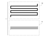
- FIG. 2 is a partially enlarged view showing the light receiving sensor 1 in FIG. 1
- FIG. 3 is a partially enlarged view showing a further enlarged portion of the light receiving sensor 1 shown in FIG. partially omitted).
- the light-receiving sensor 1 includes a light-receiving portion 11 formed of a single-pixel superconducting nanostrip arranged on a predetermined light-receiving surface area for receiving the optical signal LB, and a light-receiving portion 11 formed of, for example, the same kind of superconducting nanostrip. It has a configuration in which the vibration applying units 12 are connected in series.
- the light receiving section 11 is made of the same material and has the same shape as the photodetector element in the SNSPD
- the vibration imparting section 12 is made of the same material and has a shape similar to that of the light receiving section 11, although the shape is different from that of the light receiving section 11. .
- the photon number discriminating device 100 can be called a superconducting nanostrip (SN) type photon number discriminating device. can.
- the light receiving section 11 and the vibration imparting section 12 are formed of meandering wiring, which is formed by repeating meandering wiring of nanostrip material a plurality of times. Further, as shown in FIG. 3, the nanostrips forming the wirings of the light receiving section 11 and the vibration imparting section 12 are formed so as to satisfy the relationships represented by the following formulas (A) and (B). there is
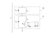
- FIG. 4 is a circuit model diagram showing an example of an equivalent circuit of the light receiving sensor 1.
- Ls and Cs indicate the inductance and capacitance (parasitic capacitance) of the light receiving section 11, respectively
- Lc and Cc indicate the inductance and capacitance (parasitic capacitance) of the vibration imparting section 12, respectively
- RN indicates the light
- the normal conduction resistance depending on the number of photons incident on the light receiving section 11 from the signal LB is shown.
- Non-Patent Document 2 for example, it is known that the normal conducting resistance RN of the light receiving section 11 is proportional to the square root of the number of photons. Also, in FIG.
- SW indicates a switch that models breaking of the superconducting state by incident photons.
- the vibration imparting section 12 can be regarded as a kind of choke coil or inductor because it has equivalently parallel-connected inductance and capacitance components.
- the switch SW is closed before photodetection, ie in the superconducting state (SC), and a bias current flows through the switch SW.
- SC superconducting state
- N normal conducting state
- the switch SW opens and the bias current flows through the normal conducting resistor RN , so that the voltage corresponding to its magnitude is will occur.
- the resonance frequency fr of this equivalent circuit can be described by the following formula (1), and from this, the electric signal (voltage signal) output from the light receiving sensor 1 has this resonance frequency fr or An amplitude (voltage) oscillatory component can occur.
- the vibration applying unit 12 by connecting the vibration applying unit 12 to the light receiving unit 11, the resonance frequency fr represented by the following formula (1) corresponding to the number of photons incident on the light receiving unit 11, or the frequency based on the resonance frequency fr is applied to the electrical signal generated by the light receiving section 11 .
- the shape parameters that affect the electrical circuit characteristics of the vibration applying unit 12, that is, the width, spacing, and total length of the nanostrips that constitute the vibration applying unit 12, and the overall width and height of the vibration applying unit 12 By adjusting at least one of them, the inductance and/or the capacitance of the vibration applying section 12 can be adjusted, so it is understood from the above formula (1) that the resonance frequency fr can be changed as desired. Therefore, by changing the electrical circuit characteristics of the vibration imparting section 12 in this way, it is possible to change the amplitude vibration component imparted to the electrical signal generated by the light receiving section 11 .
- the resonance frequency fr is lowered, thereby increasing the number of measurable photons. can improve the photon number discrimination performance.
- FIG. 5 is a schematic block diagram showing an example of the hardware configuration of the photon number identification device 100 according to an embodiment of the present disclosure from the viewpoint of a control system.
- the photon number discriminating device 100 includes the light receiving sensor 1, the attenuator 2, the bias tee 3, the amplifier 4, the constant current source 5, the amplifier 4 and the constant current source 5 of the refrigerator cryostat CR, and the external storage device 7. It has a configuration in which the control unit 6 is connected to and.
- the external storage device 7 can electromagnetically store the electrical signal waveforms output from the amplifier 4, various calculation and calculation data, and the like.
- control unit 6 includes a control calculation unit 61, a communication interface (I/F) unit 62, a storage unit 63, an input unit 64, and an output unit 65. These units communicate with each other via a bus line 66. can be connected as possible.
- a measuring instrument such as an oscilloscope for observing the waveform of an output signal
- each of these units is the measuring/signal processing unit.
- the communication I/F unit 62 can be regarded as a part responsible for an AD conversion function in an oscilloscope or the like.
- the control calculation unit 61 includes a CPU (Central Processing Unit), RAM (Random Access Memory), ROM (Read Only Memory), FPGA (Field Programmable Gate Array), ASIC (Application Specific Integrated Circuit), etc. control each component and perform various calculations.
- the communication I/F unit 62 is, for example, a communication module for communicating with other components by wire or wirelessly.
- the communication method used by the communication I/F unit 62 for communication is not particularly limited and is arbitrary, and examples thereof include LAN (Local Area Network) and USB (Universal Serial Bus). Lines can also be applied.
- the amplifier 4, the constant current source 5, and the external storage device 7 are all provided to be able to communicate with the control calculation section 61 and the like via the communication I/F section 62.
- the storage unit 63 is an auxiliary storage device such as a hard disk drive (HDD), a solid state drive (SSD), etc., and various programs executed by the control operation unit 61 (control of the constant current source 5, , a control operation program for executing processing of the electrical signal output from the amplifier 4, etc.), the waveform of the electrical signal output from the amplifier 4, other various computation results, and data including setting parameters. Further, the data and the like stored in the storage unit 63 may be stored in the external storage device 7 as appropriate.
- HDD hard disk drive
- SSD solid state drive
- the input unit 64 is an interface device for receiving various input operations from the user using the photon number identification device 100, and includes, for example, a mouse, keyboard, touch panel, an oscilloscope operation panel, buttons, switches, etc., and It can be implemented by a voice microphone, an external memory, or the like.
- the output unit 65 is an interface device for informing the user or the like using the photon number identification device 100 of various information by means of its display, audio output, print output, etc., such as a display, a speaker, a printer, etc. can be realized with
- the light sensor 1 in the cryocooler cryostat CR is cooled to a superconducting state by a command or the like from the control calculation unit 61 of the control unit 6, and the light sensor A bias current is applied to 1 from a bias tee 3 .
- a light signal LB is sent from the light source L to the light receiving portion 11 of the light receiving sensor 1
- a voltage corresponding to the amount of incident light is generated.
- the voltage signal is passed through the attenuator 2 and the bias tee 3 as an electric signal and then amplified by the amplifier 4.
- the amplified electric signal is output to the controller 6 and the output signal waveform is observed.
- the electrical signal generated by the light receiving unit 11 includes an amplitude vibration component corresponding to the number of photons incident on the light receiving unit 11 (that is, components with amplitude intensities) are given.
- the electrical signal having amplitude oscillation components obtained in this way is a superposition of a plurality of components having amplitude oscillations with different intensities depending on the number of photons over time.
- output signal voltage vertical Axis: Arbitrary unit
- the equivalent circuit shown in FIG. 4 was used as a circuit model to estimate the output signal waveform during photon detection.
- the inductance Ls of the light receiving section 11 was set to 1.6 ⁇ H, and the capacitance Cs was set to 22.4 fF.
- Example 1 represented by the solid line G0 shows the output signal waveform when the vibration imparting section 12 does not exist or when the inductance Lc and the capacitance Cc are negligible compared to the light receiving section 11 (in this respect, the reference example or the comparative example example.).
- FIG. 7 is a graph showing the actual measurement result (Example 1) of the electrical signal output from the light receiving sensor 1 of the photon number identification device 100 according to an embodiment of the present disclosure. Changes in output signal voltage (vertical axis: arbitrary unit) are shown.
- this example shows actual measurement results corresponding to the same parameter conditions as example 2 (one-dot chain line G1) in the simulation results shown in FIG.
- This result indicates that the output signal waveform of the light-receiving sensor 1 has an amplitude oscillation component, and that the number of photons can be identified from the difference in amplitude.
- the guideline of the part corresponding to 0 photons, 1 photon, and 2 or more photons is shown.
- Example 8 shows a histogram of the output signal waveform shown in FIG. 7 at a time of 126.9 ns (the time position indicated by the dashed line on the horizontal axis in FIG. 7). Vertical axis: frequency) is plotted. From this result, it was found that under the conditions of Example 1 using the photon number identification device 100, 0 photons and 1 photons can be clearly distinguished. It was confirmed that the number of photons could be identified and counted.
- FIG. 9 is a graph showing actual measurement results (Example 2) of the electrical signal output from the light receiving sensor 1 of the photon number identification device 100 according to an embodiment of the present disclosure. It was obtained in the same manner as in Example 1, except that the inductance Lc of the applying portion 12 was set to 800 nH and the capacitance Cc was set to 5.4 fF (corresponding to the resonance frequency fr of 1.31 GHz). That is, this example shows actual measurement results corresponding to the same parameter conditions as Example 3 (broken line G2) in the simulation results shown in FIG. This result also shows that the output signal waveform of the light-receiving sensor 1 has an amplitude oscillation component, and that the number of photons can be identified from the difference in amplitude. In addition, in FIG. 9, the guideline of the site
- the photon number identification device 100 can separate two-photon and three-photon or more components, which could not be distinguished by the conventional method, by expressing the amplitude oscillation part, so to speak. bottom.
- the vibration imparting section 12 is attached to the light receiving section 11 having the same configuration as the light detecting element (light receiving section) of the SNSPD. Since the connected light-receiving sensor 1 is provided, the excellent optical response characteristic of the SNSPD can be maintained as it is, and the existing SNSPD can be used almost as it is.
- the vibration imparting unit 12 imparts amplitude vibration components with different intensities according to the number of photons to the electrical signal from the light receiving sensor 1, and the number of photons can be identified and counted based on the number. Furthermore, a waveform with this amplitude oscillation can last for example on the order of 10 ns or longer.
- a filter section such as a bandpass filter may be provided after the light receiving sensor 1 .
- the photon number identification device 100 information on the number of photons can be obtained from the amplitude vibration component of the electrical signal output from the light receiving sensor 1. Therefore, even if the electrical noise is large, the noise component can be filtered out by the filter unit. By cutting and extracting only the amplitude oscillation component, more highly accurate photon number identification can be realized.
- the materials and shapes of the light receiving section 11 and the vibration imparting section 12 may be different from each other as long as an equivalent circuit as shown in FIG. 4 can be formed. Furthermore, if amplitude vibration can be imparted to the electrical signal from the light receiving section 11 using a circuit other than the equivalent circuit shown in FIG. good.
- all or part of the light receiving sensor 1, attenuator 2, bias tee 3, amplifier 4, and appropriate filter section may be integrated on a single substrate.
- bias tees 3 and amplifiers 4 having various forms and functions can be used.
- bias tees 3 may be incorporated in the amplifier 4, and the amplifier 4 cuts low frequency components. It may have a filter function.
- a plurality of vibration imparting units 12 having different electrical circuit characteristics may be switchably connected to the light receiving unit 11 of a single pixel.
- a high-speed measurement system may be used instead of a low-speed measurement system.
- the signal processing up to the identification of the number of photons described in the first and second embodiments may be automated and executed by the control calculation unit 61 of the control unit 6 or other measurement/signal processing units.
Landscapes
- Physics & Mathematics (AREA)
- General Physics & Mathematics (AREA)
- Spectroscopy & Molecular Physics (AREA)
- Photometry And Measurement Of Optical Pulse Characteristics (AREA)
- Superconductor Devices And Manufacturing Methods Thereof (AREA)
Abstract
光源からの光信号に含まれる光子数を識別するための装置であって、所定の受光面領域に配置された単一ピクセルのナノストリップから形成され、かつ、超伝導状態において光信号に対応する電気信号を生成する受光部、及び、受光部に接続され、かつ、光子数に対応する振幅振動成分を電気信号に付与する電気回路特性を有する振動付与部、を含む光検出部と、光検出部にバイアス電流を供給する電源部と、電気信号を増幅する増幅部と、光検出部及び増幅部が収容され、受光部が超伝導状態を発現する温度で作動するクライオスタットを備える光子数識別装置を提供する。
Description
本開示は、光子数識別装置及び方法に関する。
入射光の光子数を測定することができる光子数識別器は、光信号のパワーを正確に測定するための光パワーメータとして、量子光学、極微弱光測定、光センシング等の各分野で期待されている。特に、連続量光量子情報処理において、光子数を測定することによって生成し得る特殊な量子状態(非ガウス型量子状態)は、誤り耐性型万能(汎用)量子コンピュータにとって不可欠な状態である。そのための光子数識別器を実現する手法として、古くは、光子の有無のみを判別することができる単一光子検出器を時間的又は空間的に多重化することにより、擬似的な光子数識別器を構成することが試みられた。しかし、近年の研究によれば、かかる手法では一つのセンサに2光子以上入力した場合がエラーとなってしまうため、生成される非ガウス型状態の純度が下がり、非現実的であることが判明している。そこで、高速、高精度、及び多光子識別可能な光子数識別器を、複数の光検出センサを用いた多重化に依らず、すなわち単一ピクセルの光検出センサで実現することが熱望されてきた。
現在のところ、このような単一ピクセルで光子数識別性能を有する光検出センサとしては、超伝導転移端センサ(TES:Transition Edge Sensor)や超伝導ナノストリップ光子検出器(SNSPD:Superconducting NanStrip Photon Detector)が知られている。なお、SNSPDの名称における「ナノストリップ」は、「ナノワイヤ(Nanowire)」と表記又は呼称されることもあるが、本開示で用いる「ナノストリップ」との用語は「ナノワイヤ」を含み、両者は均等なものとする。
これらのうちTESは、超伝導転移温度付近まで冷却した金属薄膜に光子が入射した際の温度上昇から光子の数を測定し、100%近い検出効率も実現されており、概ね20個以上の光子を識別することができる。しかし、TESでは、光子信号の読み出しに超伝導量子干渉計と呼ばれる特別な素子計器が必要であり、その応答速度の制限から、TESの時間分解能は最も高速と思われる素子でも数ns以上となってしまう。また、TESに用いられる金属薄膜の動作温度は100mKのオーダーであり、断熱消磁冷凍機や希釈冷凍機といった大型の冷凍機が必要となるため、システム全体を設置することができる環境が制約されてしまう。
一方、SNSPDは、高感度、低雑音かつ高速動作可能な光子検出器として、前述の量子情報通信、量子光学、極微弱光センサ等の様々な分野への利用が期待されている。SNSPDにおいては、光検出素子として、所定の受光面領域に配置されたナノストリップと呼ばれる配線状の受光部分が用いられる。この受光部分は、例えば窒化ニオブ(NbN)、窒化チタンニオブ(NbTiN)、ケイ化タングステン(WSi)、ケイ化モリブデン(MoSi)等の極細線で形成され、超伝導状態において光検出素子として機能する。
ところで、SNSPDは、導入初期においては、入射光子の有無のみを判別する光検出センサとして広く使用されてきたが、出力信号の形状、特に立ち上がり部分の波形の相違から、光子数を測定可能な光子数識別器としても使用できることが、近年の研究によって明らかになってきている(例えば非特許文献1~3)。このようなSNSPD型の光子数識別器の時間分解能は10psオーダーであり、前述したTESに比して、100倍程度高速での応答特性を有している。また、SNSPDに用いられる上記受光部分は、例えば、小型のパルスチューブ冷凍機やギフォード・マクマホン(GM)冷凍機等によって作動可能であり、これによりシステム全体の規模を小型化して省スペース化を図り得るという大きな利点を有する。
C. Cahall et al., Optica 4, 1534-1535 (2017)
K. L. Nicolich et al., Phys. Rev. Appl. 12, 034020 (2019)
M. Endo et al., Opt. Express 29, 11728-11738 (2021)
しかし、SNSPDで測定される信号波形のうち光子数の情報を有するは、立ち上がりの100ps程度の部分でしかないことが判明しており、そのため、SNSPDの後段に、帯域が十分に広くない増幅回路や計器を備える低速の測定系を用いる場合には、正確な光子数識別ができないという問題があった。換言すれば、SNSPDにより従来の手法で光子数の情報を得るには、100psオーダー以下の時間単位で信号波形をリアルタイムで解析しなければならず、また、雑音の影響も受け易いため、非常に高速で特殊な測定系(例えば、高速AD変換器とFPGA又はASIC等の高速回路との組み合わせ等)による複雑な処理が不可欠であり、コストも増大する傾向にあった。
そこで、本開示は、かかる事情に鑑みてなされたものであり、SNSPDの優れた光応答特性(光検出特性)を保持しつつ、雑音の影響を軽減することができ、かつ、帯域が狭い低速の測定系を用いた場合でも、正確かつ簡便に優れた光子数識別性を実現することが可能であり、これらにより、経済性、操作性、及び汎用性にも優れる光子数識別装置及び方法を提供することを目的とする。
〔1〕本開示に係る光子数識別装置の一例は、光源からの光信号に含まれる光子数を識別するための装置であって、所定の受光面領域に配置された単一ピクセルのナノストリップから形成され、かつ、超伝導状態において前記光信号に対応する電気信号を生成する受光部、及び、前記受光部に(直列又は並列に)接続され、かつ、光子数に対応する振幅振動成分を前記電気信号に付与する電気回路特性を有する振動付与部、を含む光検出部と、前記光検出部にバイアス電流を供給する電源部と、前記電気信号を増幅する増幅部と、前記光検出部及び前記増幅部が収容され、前記受光部が超伝導状態を発現する温度で作動するクライオスタットを備える。
かかる構成では、受光部として、クライオスタットによって超伝導状態となるように冷却されるSNSPDの光検出素子と同等の構成を採用し得る。そして、その受光部に振動付与部を追設することにより、光源からの光信号を受信した受光部で生成する電気信号に、光子数に対応する振幅振動成分(すなわち光子数に応じた振動特性を有する成分)が付与される。よって、光検出部から出力される電気信号は、従来のSNSPDからの出力信号とは異なり、各光子数に応じて異なる強度の振幅振動を有する複数の成分が重畳され、例えば10ns程度以上持続する波形を示現する。従って、SNSPDで必要であった立ち上がり部分の高速での信号処理が不要となり、また、光検出部からの電気信号又はその増幅信号波形における強度が異なる振幅振動成分の数に基づいて、光子数の識別及び計数が可能となる。
〔2〕上記態様において、前記振幅振動成分の周波数は、下記式(1);
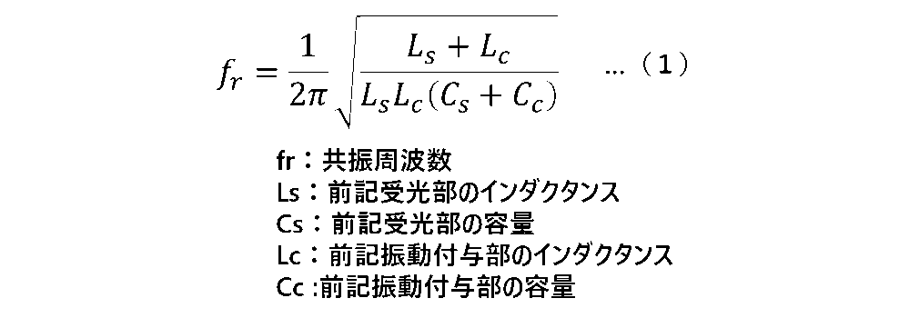
で表される共振周波数fr、又は、該共振周波数frに基づく周波数であってもよい。
本開示における光検出部は、受光部及び振動付与部が、ともにそれぞれ、電気素子的な内部要素として所定のインダクタンスLs,Lcと所定の容量(寄生容量)Cs,Ccを有する等価回路と捉え得るので、両者の接続により、上記式(1)で表される共振周波数が生起され、このような簡便な素子構造により、受光部で生成される電気信号に振幅振動成分が付与され、かつ、雑音の発生を極力抑制することができる。
〔3〕上記態様において、より具体的には、前記振動付与部が、前記受光部と同等又は同種の材料から構成されてもよい。このようにすれば、受光部と振動付与部をパターン形成し易くなり、また、構造及び性能シミュレーションや実設計を行い易くなる。
〔4〕上記態様において、前記振動付与部を、前記受光部のナノストリップとは形状が異なるナノストリップから形成してもよい。このようにすれば、受光部と振動付与部を更にパターン形成し易くなり、また、構造及び性能シミュレーションや実設計を更に行い易くなる。
〔5〕上記態様において、前記振動付与部のナノストリップの線幅を、前記受光部のナノストリップの線幅よりも太くし、前記振動付与部のナノストリップの間隔を、前記受光部のナノストリップの間隔よりも広くしてもよい。本発明人の知見によれば、かかる構成を採用することにより、受光部からの電気信号に、前述した振幅振動成分をより一層付与し易くなり、また、電気信号波形において、光子数に応じた振幅成分をより明確に弁別し易くなることが確認された。
〔6〕上記態様において、更に具体的には、前記受光部及び前記振動付与部を、蛇行配線が複数回繰り返されて成るミアンダ配線から形成してもよい。このようにすれば、ナノストリップを用いた受光部及び振動付与部の形成面積を狭小化することができ、光検出部の軽薄化及び小型化を促進することができる。
〔7〕上記態様において、前記増幅部に接続され、前記電気信号の増幅信号を受信し、該増幅信号波形における強度が異なる前記振幅振動成分を弁別する信号処理部を更に備えてもよい。この信号処理部により、前記〔1〕で述べたような、光検出部からの電気信号の増幅信号波形における異なる強度の振幅振動成分の数に基づいた光子数の識別及び計数を、確実にかつ一層簡便に行うことができる。
〔8〕上記態様において、前記光検出部と前記増幅部との間に接続され、前記電気信号を受信し、該電気信号を減衰させる減衰部、及び/又は、該電気信号の所定の周波数成分をフィルタリングするフィルタ部を更に備えてもよい。この場合、減衰部により、光検出からの電気信号に含まれる光子数の情報を、その後の信号処理に適するように適宜調節制御することができる。また、本開示では、出力される電気信号の振幅振動成分から光子数の情報が得られるところ、たとえ電気的な雑音が大きい場合であっても、フィルタ部(バンドパスフィルタ等)によって雑音成分をカットして振幅振動成分のみを取り出すことができる。
〔9〕また、本開示に係る光子数識別方法の一例は、本開示に係る光子数識別装置を用いて好適に実施することができる方法である。すなわち、本例は、光源からの光信号に含まれる光子数を識別するための方法であって、本開示による光子数識別装置を準備するステップと、前記クライオスタットが、前記受光部が超伝導状態を発現する温度で動作するステップと、前記電源部が、前記光検出部にバイアス電流を供給するステップと、前記光検出部の前記受光部が、超伝導状態において前記光信号に対応する電気信号を生成するステップと、前記光検出部の前記振動付与部が、光子数に対応する振幅振動成分を前記電気信号に付与するステップと、前記増幅部が、前記電気信号を増幅するステップを含む。
〔10〕上記態様において、前記光子数識別装置は、前記信号処理部を更に備えており、該信号処理部が、前記増幅信号波形における異なる強度の前記振幅振動成分を弁別するステップを更に含んでもよい。
〔11〕上記態様において、前記振動付与部の電気回路特性を変更することにより、前記光子数に対応する振幅振動成分を変化させるステップを更に含んでもよい。このようにすれば、光検出部の上記式(1)で示す共振周波数frが変化し、その結果、光子数に応じた振幅振動成分を有する電気信号の周波数、振幅、波形形状、縮退数等といった種々の特性を調整し得る。
なお、本開示において、1つの「部」や「装置」(「機」、「器」、「手段」、「機構」、「システム」等と言い換えることも可能な概念である。以下同様。)、及びそれらの構成部品や構成要素が有する機能が、2つ以上の物理的手段や装置等によって実現されてもよく、或いは、2つ以上の「部」や「装置」、及びそれらの構成部品や構成要素の機能が1つの物理的手段や装置等によって実現されてもよい。
本開示によれば、SNSPDの光検出素子と同等の構成を有する受光部に振動付与部を接続することにより光検出部を構成するので、SNSPDの優れた光応答特性をそのまま保持することができる。また、振動付与部が、受光部からの電気信号に、光子数に応じた異なる強度の振幅振動成分を付与し、その数に基づいて、光子数の識別及び計数を行うことができる。さらに、この振幅振動を有する波形は、例えば10ns程度以上持続する。よって、SNSPDで必要であった立ち上がり部分の高速での信号処理が不要となる。また、そのように高速での信号処理が不要であるので、複雑な信号処理に依らずとも雑音の影響を軽減しつつ、帯域が狭い低速の測定系を用いた場合でも、高分解能で優れた光子数識別性能を、簡易な構成で十分に実現することができる。その結果、光子数識別における経済性、操作性、及び汎用性を従来に比して格段に向上させることができ、かつ、従来の高速信号処理では困難であった多チャネル化も可能となる。
以下、本開示の一例に係る実施形態について、図面を参照して説明する。但し、以下に説明する実施形態は、あくまでも例示であり、以下に明示しない種々の変形や技術の適用を排除する意図ではない。すなわち、本開示の一例は、その趣旨を逸脱しない範囲で種々変形して実施することができる。また、以下の図面の記載において、同一又は類似の部分には同一又は類似の符号を付し、図面は模式的なものであって、必ずしも実際の寸法や比率等とは一致しない。さらに、図面相互間においても互いの寸法の関係や比率が異なる部分が含まれていることがある。また、以下に説明する実施形態は本開示の一部の実施形態であって全ての実施形態ではない。さらに、本開示の実施形態に基づいて、当業者が創造性のある行為を必要とせずに得られる他の実施形態は、いずれも本開示の保護範囲に含まれる。
[光子数識別装置の構成例]
図1は、本開示の一実施形態に係る光子数識別装置の一例の概略構成を示す平面図である。光子数識別装置100は、本開示に係る光子数識別方法を実行するための装置であり、適宜の光源Lから光学系OSによって光信号LBが導出又は送出される受光センサ1、その受光センサ1に順次接続された減衰器2、バイアスティー3、及び増幅器4を備える。これらの受光センサ1、減衰器2、バイアスティー3、及び増幅器4は、冷凍機クライオスタットCRの内部に収容設置されている。また、バイアスティー3は、冷凍機クライオスタットCRの外部に設けられた定電流源5に接続されており、これにより、冷凍機クライオスタットCRの外部から、バイアスティー3を介して、受光センサ1に所定のバイアス電流が印加される。さらに、例えば増幅器4の出力側、定電流源5、及び冷凍機クライオスタットCRには、冷凍機クライオスタットCRの外部に設けられた制御部6が接続されている。また、冷凍機クライオスタットCRの内部及び外部の各要素機器の接続は、同軸ケーブルによって配線されると好ましく、図1においては、受光センサ1と減衰器2、及び、増幅器4と制御部6の接続配線が同軸ケーブルKによって接続されている状態を例示した。なお、制御部6として、或いは、制御部6に代えて、出力信号の波形観測を行うオシロスコープ等の測定器(測定・信号処理部)を用いてもよく、その場合、その測定・信号処理部と、定電流源5、及び、冷凍機クライオスタットCRとは独立して作動し得るので、接続を不要としてもよい。
図1は、本開示の一実施形態に係る光子数識別装置の一例の概略構成を示す平面図である。光子数識別装置100は、本開示に係る光子数識別方法を実行するための装置であり、適宜の光源Lから光学系OSによって光信号LBが導出又は送出される受光センサ1、その受光センサ1に順次接続された減衰器2、バイアスティー3、及び増幅器4を備える。これらの受光センサ1、減衰器2、バイアスティー3、及び増幅器4は、冷凍機クライオスタットCRの内部に収容設置されている。また、バイアスティー3は、冷凍機クライオスタットCRの外部に設けられた定電流源5に接続されており、これにより、冷凍機クライオスタットCRの外部から、バイアスティー3を介して、受光センサ1に所定のバイアス電流が印加される。さらに、例えば増幅器4の出力側、定電流源5、及び冷凍機クライオスタットCRには、冷凍機クライオスタットCRの外部に設けられた制御部6が接続されている。また、冷凍機クライオスタットCRの内部及び外部の各要素機器の接続は、同軸ケーブルによって配線されると好ましく、図1においては、受光センサ1と減衰器2、及び、増幅器4と制御部6の接続配線が同軸ケーブルKによって接続されている状態を例示した。なお、制御部6として、或いは、制御部6に代えて、出力信号の波形観測を行うオシロスコープ等の測定器(測定・信号処理部)を用いてもよく、その場合、その測定・信号処理部と、定電流源5、及び、冷凍機クライオスタットCRとは独立して作動し得るので、接続を不要としてもよい。
このとおり、これらの光子数識別装置100、受光センサ1、減衰器2、増幅器4、制御部6(オシロスコープ等の測定・信号処理部を含む。)、及び冷凍機クライオスタットCRが、それぞれ、本開示における「光子数識別装置」、「光検出部」、「減衰部」、「増幅部」、「信号処理部」、及び「クライオスタット」の一例に相当する。また、バイアスティー3及び定電流源5が、本開示における「電源部」の一例に相当する。
ここで、図2は、図1における受光センサ1を拡大して示す部分拡大図であり、図3は、図2に示す受光センサ1の一部を更に拡大して示す部分拡大図である(一部省略)。受光センサ1は、光信号LBを受光するための所定の受光面領域に配置された単一ピクセルの超伝導ナノストリップから形成された受光部11に、例えば同種の超伝導ナノストリップから形成された振動付与部12が直列に接続された構成を有する。これらのうち受光部11は、SNSPDにおける光検出素子と同種材料及び同等形状で形成されており、振動付与部12は、受光部11と形状は異なるものの、同種材料及び近似形状で形成されている。このように、受光部11として、SNSPDにおける光検出素子をほぼそのまま利用することができるので、光子数識別装置100は、超伝導ナノストリップ(SN:Superconducting NanStrip)型の光子数識別装置ということもできる。
具体的には、受光部11及び振動付与部12は、図2及び図3に示すとおり、ナノストリップ材料の蛇行配線が複数回繰り返されて成るミアンダ配線から形成されている。また、図3に示すように、受光部11及び振動付与部12のそれぞれの配線を構成するナノストリップは、下記式(A)及び式(B)で表される関係を満たすように形成されている。
振動付与部12のナノストリップの線幅>受光部11のナノストリップの線幅 …(A)
振動付与部12のナノストリップの間隔>受光部11のナノストリップの間隔 …(B)
より具体的には、受光部11のナノストリップの線幅及び間隔が数10nmであり、振動付与部12のナノストリップの線幅及び間隔が数100nmであり、受光部11及び振動付与部12の全体幅が数10~数100μmであり、その全体高さが数10μmである例が挙げられる。
振動付与部12のナノストリップの間隔>受光部11のナノストリップの間隔 …(B)
より具体的には、受光部11のナノストリップの線幅及び間隔が数10nmであり、振動付与部12のナノストリップの線幅及び間隔が数100nmであり、受光部11及び振動付与部12の全体幅が数10~数100μmであり、その全体高さが数10μmである例が挙げられる。
ここで、図4は、受光センサ1の等価回路の一例を示す回路モデル図である。図4において、Ls,Csは、それぞれ受光部11のインダクタンス及び容量(寄生容量)を示し、Lc,Ccは、それぞれ振動付与部12のインダクタンス及び容量(寄生容量)を示し、RNは、光信号LBから受光部11に入射した光子数に依存する常伝導抵抗を示す。なお、受光部11の常伝導抵抗RNは、例えば非特許文献2によれば、光子数の平方根に比例することが知られている。また、図4において、SWは、入射した光子により超伝導状態が壊れることをモデル化したスイッチを示す。なお、この回路モデル図より、振動付与部12は、等価的に、並列接続されたインダクタンス及び容量成分を有することから、一種のチョークコイル又はインダクタと看做すこともできる。
図4に模式的に示すとおり、スイッチSWは、光検出前つまり超伝導状態(SC)のときは閉じており、バイアス電流はスイッチSWを流れる。一方、光子の入射による熱の発生により超伝導状態が壊れて常伝導状態(N)になると、スイッチSWは開き、バイアス電流は常伝導抵抗RNを流れるので、その大きさに応じた電圧が発生することとなる。この等価回路の共振周波数frは、下記式(1)のように記述することができ、このことから、受光センサ1から出力される電気信号(電圧信号)には、この共振周波数fr又はそれに基づく振幅(電圧)振動成分が生じ得る。すなわち、受光部11に振動付与部12が接続されることにより、受光部11に入射した光子数に対応した下記式(1)で表される共振周波数fr、又は、該共振周波数frに基づく周波数を有する振幅振動成分が、受光部11で生成される電気信号に付与される。
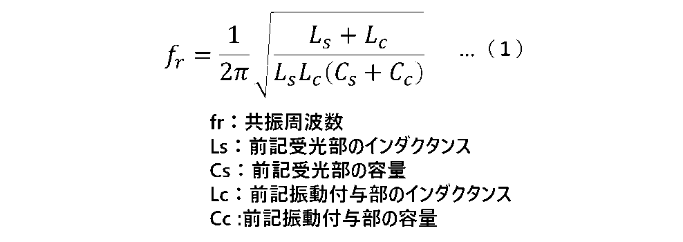
また、振動付与部12の電気回路特性に影響を与える形状パラメータ、つまり、振動付与部12を構成するナノストリップの幅、間隔、及び全長、並びに、振動付与部12の全体幅及び全体高さの少なくとも何れかを調節することにより、振動付与部12のインダクタンス及び/又は容量を調節し得るので、上記式(1)より、共振周波数frを所望に変化させ得ることが理解される。よって、このように振動付与部12の電気回路特性を変更することにより、受光部11で生成される電気信号に付与される振幅振動成分を変化させることが可能となる。さらに、より具体的には、例えば、振動付与部12のナノストリップの全長を大きくしてインダクタンスLc及び容量Ccを大きくすることで、共振周波数frを下げることにより、測定可能な光子数を増大させて光子数識別性能を向上させることができる。
[制御系のハードウェア構成例]
図5は、本開示の一実施形態に係る光子数識別装置100のハードウェア構成の一例を、制御系としての観点から示す概略ブロック図である。光子数識別装置100は、前述した受光センサ1、減衰器2、バイアスティー3、増幅器4、定電流源5、及び、冷凍機クライオスタットCRのうち増幅器4及び定電流源5と、外部記憶装置7とに制御部6が接続された構成を有する。また、外部記憶装置7は、増幅器4から出力される電気信号波形や種々の演算及び計算データ等を電磁的に記憶することができる。さらに、制御部6は、制御演算部61、通信インタフェース(I/F)部62、記憶部63、入力部64、及び出力部65を含み、これらの各部はバスライン66を介して相互に通信可能に接続され得る。なお、制御部6として、或いは、制御部6に代えて、出力信号の波形観測を行うオシロスコープ等の測定器(測定・信号処理部)を用いる場合、これらの各部は、その測定・信号処理部に備わる機能部と看做すこともでき、例えば、通信I/F部62は、オシロスコープ等におけるAD変換機能を担う部分と捉え得る。
図5は、本開示の一実施形態に係る光子数識別装置100のハードウェア構成の一例を、制御系としての観点から示す概略ブロック図である。光子数識別装置100は、前述した受光センサ1、減衰器2、バイアスティー3、増幅器4、定電流源5、及び、冷凍機クライオスタットCRのうち増幅器4及び定電流源5と、外部記憶装置7とに制御部6が接続された構成を有する。また、外部記憶装置7は、増幅器4から出力される電気信号波形や種々の演算及び計算データ等を電磁的に記憶することができる。さらに、制御部6は、制御演算部61、通信インタフェース(I/F)部62、記憶部63、入力部64、及び出力部65を含み、これらの各部はバスライン66を介して相互に通信可能に接続され得る。なお、制御部6として、或いは、制御部6に代えて、出力信号の波形観測を行うオシロスコープ等の測定器(測定・信号処理部)を用いる場合、これらの各部は、その測定・信号処理部に備わる機能部と看做すこともでき、例えば、通信I/F部62は、オシロスコープ等におけるAD変換機能を担う部分と捉え得る。
制御演算部61は、CPU(Central Processing Unit)、RAM(Random Access Memory)、ROM(Read Only Memory)、FPGA(Field Programmable Gate Array)、ASIC(Application Specific Integrated Circuit)等を含み、情報処理に応じて各構成要素の制御及び各種演算を行う。また、通信I/F部62は、例えば、有線又は無線により他の構成要素と通信するための通信モジュールである。通信I/F部62が通信に用いる通信方式は特に制限されず任意であり、例えば、LAN(Local Area Network)やUSB(Universal Serial Bus)等が挙げられ、バスライン66と同等の適宜の通信線を適用することもできる。増幅器4、定電流源5、及び外部記憶装置7は、ともに、この通信I/F部62を介して、制御演算部61等と通信可能に設けられている。
記憶部63は、例えばハード・ディスク・ドライブ(HDD)、ソリッド・ステート・ドライブ(SSD)等の補助記憶装置であり、制御演算部61で実行される各種プログラム(定電流源5の制御、及び、増幅器4から出力された電気信号の処理を実行するための制御演算プログラム等)、増幅器4から出力された電気信号波形、その他の各種演算結果及び設定パラメータ等を含むデータを記憶する。また、記憶部63に記憶されたデータ等は、外部記憶装置7に適宜記憶させてもよい。
入力部64は、光子数識別装置100を利用するユーザからの各種入力操作を受け付けるためのインタフェースデバイスであり、例えば、マウス、キーボード、タッチパネル、例えばオシロスコープの操作パネル、ボタン、及びスイッチ等、並びに、音声マイク、外部メモリ等で実現し得る。また、出力部65は、光子数識別装置100を利用するユーザ等へ、各種情報を、その表示、音声出力、印刷出力等により報知するためのインタフェースデバイスであり、例えば、ディスプレイ、スピーカ、プリンタ等で実現し得る。
[光子数識別装置の動作例]
以上の構成を有する光子数識別装置100では、制御部6の制御演算部61からの指令等により、冷凍機クライオスタットCR内の受光センサ1が超伝導状態となるように冷却され、また、受光センサ1にバイアスティー3からバイアス電流が印加される。この状態で受光センサ1の受光部11に、光源Lから光信号LBが送出されると、入射した光量に応じた電圧が発生する。また、その電圧信号が電気信号として減衰器2及びバイアスティー3を介した後、増幅器4によって増幅され、さらに、その増幅電気信号が制御部6へ出力されて出力信号波形が観測される。
以上の構成を有する光子数識別装置100では、制御部6の制御演算部61からの指令等により、冷凍機クライオスタットCR内の受光センサ1が超伝導状態となるように冷却され、また、受光センサ1にバイアスティー3からバイアス電流が印加される。この状態で受光センサ1の受光部11に、光源Lから光信号LBが送出されると、入射した光量に応じた電圧が発生する。また、その電圧信号が電気信号として減衰器2及びバイアスティー3を介した後、増幅器4によって増幅され、さらに、その増幅電気信号が制御部6へ出力されて出力信号波形が観測される。
このとき、受光部11に振動付与部12が接続されているので、受光部11で生成された電気信号には、受光部11に入射した光子数に対応する振幅振動成分(すなわち光子数に応じた振幅強度を有する成分)が付与される。こうして得られる振幅振動成分を有する電気信号は、従来のSNSPDからの出力信号とは異なり、時間経過とともに各光子数に応じて異なる強度の振幅振動を有する複数の成分が重畳されたものとなる。
(シミュレーション例)
図6は、本開示の一実施形態に係る光子数識別装置100の受光センサ1から出力される電気信号のシミュレーション結果の一例を示すグラフであり、時間(横軸)経過に対する出力信号電圧(縦軸:任意単位)の変化を示す(立ち上がり時刻を「時間=0ns」として規格化した。)。このシミュレーションは、図4に示す等価回路を回路モデルとして用い、光子検出時の出力信号波形を推算したものであり、受光部11の回路パラメータは、図6に示す例1~3について共通とし、受光部11のインダクタンスLs=1.6μH、及び、容量Cs=22.4fFと設定した。
図6は、本開示の一実施形態に係る光子数識別装置100の受光センサ1から出力される電気信号のシミュレーション結果の一例を示すグラフであり、時間(横軸)経過に対する出力信号電圧(縦軸:任意単位)の変化を示す(立ち上がり時刻を「時間=0ns」として規格化した。)。このシミュレーションは、図4に示す等価回路を回路モデルとして用い、光子検出時の出力信号波形を推算したものであり、受光部11の回路パラメータは、図6に示す例1~3について共通とし、受光部11のインダクタンスLs=1.6μH、及び、容量Cs=22.4fFと設定した。
実線G0で表す例1は、振動付与部12が存在しないか、或いは、受光部11に比してインダクタンスLc及び容量Ccが無視できる場合の出力信号波形を示す(この点において、参考例又は比較例である。)。また、一点鎖線G1で表す例2は、振動付与部12を有し、そのインダクタンスLc=400nH、及び、容量Cc=2.7fF(共振周波数fr=1.78GHz相当)としたときの出力信号波形を示す。さらに、破線G2で表す例3は、振動付与部12を有し、そのインダクタンスLc=800nH,容量Cc=5.4fF(共振周波数fr=1.31GHz相当)としたときの出力信号波形を示す。
これらの例1~3として示す結果より、受光部11に振動付与部12を追設した光子数識別装置100によれば、受光センサ1からの出力信号波形に振幅振動成分が発現することが理解される。また、このような振幅振動を有する出力信号波形(一点鎖線G1及び破線G2)が5ns程度経過した時点でも減衰しておらず、10ns程度以上持続することが示唆される。さらに、振動付与部12の電気回路特性を変更することにより、出力信号の周波数や振幅が変化し得ることも判明した。
そこで、光子数識別装置100と同等の構成を有する実機を試作し、光源Lとしてパルス光を用いて、その光子数識別性能を評価した。
(実施例1)
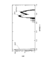
図7は、本開示の一実施形態に係る光子数識別装置100の受光センサ1から出力される電気信号の実測結果(実施例1)を示すグラフであり、実際の時間(横軸)経過に対する出力信号電圧(縦軸:任意単位)の変化を示す。本実施例は、受光センサ1の回路パラメータを、受光部11のインダクタンスLs=1.6μH、及び、容量Cs=22.4fFとし、また、振動付与部12のインダクタンスLc=400nH、及び、容量Cc=2.7fF(共振周波数fr=1.78GHz相当)として得られた出力信号波形を8192本重ねて得たものである。すなわち、本実施例は、図6に示すシミュレーション結果における例2(一点鎖線G1)と同じパラメータ条件に対応する実測結果を示す。この結果は、受光センサ1の出力信号波形が振幅振動成分を有しており、その振幅の相違から光子数を識別可能であることを示すものである。なお、図7中に、0光子、1光子、及び2光子以上に対応する部位の目安を示す。
図7は、本開示の一実施形態に係る光子数識別装置100の受光センサ1から出力される電気信号の実測結果(実施例1)を示すグラフであり、実際の時間(横軸)経過に対する出力信号電圧(縦軸:任意単位)の変化を示す。本実施例は、受光センサ1の回路パラメータを、受光部11のインダクタンスLs=1.6μH、及び、容量Cs=22.4fFとし、また、振動付与部12のインダクタンスLc=400nH、及び、容量Cc=2.7fF(共振周波数fr=1.78GHz相当)として得られた出力信号波形を8192本重ねて得たものである。すなわち、本実施例は、図6に示すシミュレーション結果における例2(一点鎖線G1)と同じパラメータ条件に対応する実測結果を示す。この結果は、受光センサ1の出力信号波形が振幅振動成分を有しており、その振幅の相違から光子数を識別可能であることを示すものである。なお、図7中に、0光子、1光子、及び2光子以上に対応する部位の目安を示す。
また、図8は、図7に示す出力信号波形の時間=126.9nsの時点(図7の横軸に破線を付した時間位置)におけるヒストグラムを示し、各信号電圧(横軸)の計数(縦軸:頻度)をプロットしたグラフである。この結果より、光子数識別装置100を用いた実施例1の条件では、0光子と1光子を明確に区別できることが判明し、また、2光子以上は縮退していると認められるものの、複数の光子数を識別及び計数し得ることが確認された。
(実施例2)
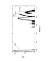
図9は、本開示の一実施形態に係る光子数識別装置100の受光センサ1から出力される電気信号の実測結果(実施例2)を示すグラフであり、受光センサ1の回路パラメータを、振動付与部12のインダクタンスLc=800nH、及び、容量Cc=5.4fF(共振周波数fr=1.31GHz相当)としたこと以外は、実施例1と同様にして得られたものである。すなわち、本実施例は、図6に示すシミュレーション結果における例3(破線G2)と同じパラメータ条件に対応する実測結果を示す。この結果も、受光センサ1の出力信号波形が振幅振動成分を有しており、その振幅の相違から光子数を識別可能であることを示すものである。なお、図9中に、0光子、1光子、2光子、及び3光子以上に対応する部位の目安を示す。
図9は、本開示の一実施形態に係る光子数識別装置100の受光センサ1から出力される電気信号の実測結果(実施例2)を示すグラフであり、受光センサ1の回路パラメータを、振動付与部12のインダクタンスLc=800nH、及び、容量Cc=5.4fF(共振周波数fr=1.31GHz相当)としたこと以外は、実施例1と同様にして得られたものである。すなわち、本実施例は、図6に示すシミュレーション結果における例3(破線G2)と同じパラメータ条件に対応する実測結果を示す。この結果も、受光センサ1の出力信号波形が振幅振動成分を有しており、その振幅の相違から光子数を識別可能であることを示すものである。なお、図9中に、0光子、1光子、2光子、及び3光子以上に対応する部位の目安を示す。
また、図10は、図9に示す出力信号波形の時間=126.4nsの時点(図9の横軸に破線を付した時間位置)におけるヒストグラムを示し、各信号電圧(横軸)の計数(縦軸:頻度)をプロットしたグラフである。この結果より、光子数識別装置100を用いた実施例2の条件では、0光子、1光子、及び2光子(つまり2光子まで)を明確に区別できることが判明し、また、3光子以上は縮退していると認められるものの、実施例1と同様に、複数の光子数を識別及び計数し得ることが確認された。
また、本実施例では、図9に示されるように、振動部分に繋がる出力信号の立ち上がり部分では波形が2つ(2本)に縮退しているものの、時間が経過して振幅振動を示現する部分では、2つのうちの一方の縮退が解けている点が注目される。つまり、従来手法では判別が不可能であった2光子と3光子以上の成分が、光子数識別装置100によれば、振幅振動部分をいわば発現させることによって分離することが可能であることが判明した。
このように構成された光子数識別装置100、及び、それを用いた光子数識別方法によれば、SNSPDの光検出素子(受光部分)と同等の構成を有する受光部11に振動付与部12を接続した受光センサ1を備えるので、SNSPDの優れた光応答特性をそのまま保持することができ、既存のSNSPDをほぼそのまま流用することができる。また、振動付与部12が、受光センサ1からの電気信号に、光子数に応じた異なる強度の振幅振動成分を付与し、その数に基づいて、光子数の識別及び計数を行うことができる。さらに、この振幅振動を有する波形は、例えば10ns程度以上持続し得る。よって、SNSPDで必要であった立ち上がり部分の高速での信号処理が不要となり、信号処理系の簡素化が可能となる。また、そのように高速での信号処理が不要であるので、複雑な信号処理に依らずとも雑音の影響を軽減しつつ、帯域が狭い低速の測定系を用いた場合でも、高分解能で優れた光子数識別性能を、簡易な構成で十分に実現することができる。その結果、光子数識別における経済性、操作性、及び汎用性を従来に比して格段に向上させることができ、かつ、従来の高速信号処理では困難であった多チャネル化も可能となる。
以上、本開示の一例としての上記実施形態について詳細に説明してきたが、上述したとおり、前述した説明はあらゆる点において本開示の一例を示すに過ぎず、本開示の範囲を逸脱することなく種々の改良や変形を行うことができることはいうまでもない。また、上記実施形態は、部分的に置換、削除、又は組み合わせて構成することも可能である。
例えば、受光センサ1の後段に、バンドパスフィルタ等のフィルタ部を設けてもよい。光子数識別装置100によれば、受光センサ1から出力される電気信号の振幅振動成分から光子数の情報が得られるので、電気的な雑音が大きい場合であっても、フィルタ部によって雑音成分をカットして振幅振動成分のみを取り出すことにより、更に高精度な光子数識別を実現することができる。また、受光部11と振動付与部12の材料や形状は、図4に示すような等価回路を構成することができれば、互いに異なっていてもよい。さらに、図4に示すような等価回路以外でも、受光部11からの電気信号に振幅振動を付与することができる場合には、振動付与部12は、受光部11に並列に接続されていてもよい。
また、受光センサ1、減衰器2、バイアスティー3、及び増幅器4、並びに適宜のフィルタ部(用いる場合)の全部又は一部を、単一の基板に集積化してもよい。またさらに、バイアスティー3や増幅器4として、種々の形態や機能を有するものを用いることができ、例えば、バイアスティー3が増幅器4に内蔵されていてもよく、増幅器4が低周波成分をカットするフィルタ機能を備えていてもよい。さらにまた、単一ピクセルの受光部11に、電気回路特性が互いに異なる複数の振動付与部12を切り替え可能に接続してもよい。加えて、低速の測定系ではなく、高速の測定系を使用してももちろんよく、この場合でも、従来手法に比して多光子識別性能が向上することはいうまでもない。また、実施例1及び2で説明した光子数識別までの信号処理を、制御部6の制御演算部61やその他の測定・信号処理部によって自動化して実行しても構わない。
Claims (11)
- 光源からの光信号に含まれる光子数を識別するための装置であって、
所定の受光面領域に配置された単一ピクセルのナノストリップから形成され、かつ、超伝導状態において前記光信号に対応する電気信号を生成する受光部、及び、前記受光部に接続され、かつ、光子数に対応する振幅振動成分を前記電気信号に付与する電気回路特性を有する振動付与部、を含む光検出部と、
前記光検出部にバイアス電流を供給する電源部と、
前記電気信号を増幅する増幅部と、
前記光検出部及び前記増幅部が収容され、前記受光部が超伝導状態を発現する温度で作動するクライオスタットと、
を備える、光子数識別装置。 - 前記振幅振動成分は、下記式(1);

で表される共振周波数fr、又は、該共振周波数frに基づく周波数を有する、
請求項1に記載の光子数識別装置。 - 前記振動付与部は、前記受光部と同等又は同種の材料から構成される、請求項1又は2に記載の光子数識別装置。
- 前記振動付与部は、前記受光部のナノとは形状が異なるナノから形成される、請求項1~3の何れかに記載の光子数識別装置。
- 前記振動付与部のナノストリップの線幅は、前記受光部のナノストリップの線幅よりも太く、
前記振動付与部のナノストリップの間隔は、前記受光部のナノストリップの間隔よりも広い、
請求項4に記載の光子数識別装置。 - 前記受光部及び前記振動付与部は、蛇行配線が複数回繰り返されて成るミアンダ配線から形成される、請求項4又は5に記載の光子数識別装置。
- 前記増幅部に接続され、前記電気信号の増幅信号を受信し、該増幅信号波形における異なる強度の前記振幅振動成分を弁別する信号処理部を更に備える、請求項1~6の何れかに記載の光子数識別装置。
- 前記光検出部と前記増幅部との間に接続され、前記電気信号を受信し、該電気信号を減衰させる減衰部、及び/又は、該電気信号の所定の周波数成分をフィルタリングするフィルタ部を更に備える、請求項1~7の何れかに記載の光子数識別装置。
- 光源からの光信号に含まれる光子数を識別するための方法であって、
所定の受光面領域に配置された単一ピクセルのナノストリップから形成された受光部、及び、特定の電気回路特性を有して前記受光部に接続された振動付与部を含む光検出部、電源部、増幅部、並びに、前記光検出部及び前記増幅部が収容されたクライオスタットを備える光子数識別装置を準備するステップと、
前記クライオスタットが、前記受光部が超伝導状態を発現する温度で動作するステップと、
前記電源部が、前記光検出部にバイアス電流を供給するステップと、
前記光検出部の前記受光部が、超伝導状態において前記光信号に対応する電気信号を生成するステップと、
前記光検出部の前記振動付与部が、光子数に対応する振幅振動成分を前記電気信号に付与するステップと、
前記増幅部が、前記電気信号を増幅するステップと、
を含む、光子数識別方法。 - 前記光子数識別装置は、前記増幅部に接続されて前記電気信号の増幅信号を受信する信号処理部を更に備え、
前記信号処理部が、前記増幅信号波形における異なる強度の前記振幅振動成分を弁別するステップを更に含む、請求項9に記載の光子数識別方法。 - 前記振動付与部の電気回路特性を変更することにより、前記光子数に対応する振幅振動成分を変化させるステップを更に含む、請求項9又は10に記載の光子数識別方法。
Applications Claiming Priority (2)
| Application Number | Priority Date | Filing Date | Title |
|---|---|---|---|
| JP2022016708A JP2023114467A (ja) | 2022-02-04 | 2022-02-04 | 光子数識別装置及び方法 |
| JP2022-016708 | 2022-02-04 |
Publications (1)
| Publication Number | Publication Date |
|---|---|
| WO2023149331A1 true WO2023149331A1 (ja) | 2023-08-10 |
Family
ID=87552263
Family Applications (1)
| Application Number | Title | Priority Date | Filing Date |
|---|---|---|---|
| PCT/JP2023/002423 Ceased WO2023149331A1 (ja) | 2022-02-04 | 2023-01-26 | 光子数識別装置及び方法 |
Country Status (2)
| Country | Link |
|---|---|
| JP (1) | JP2023114467A (ja) |
| WO (1) | WO2023149331A1 (ja) |
Citations (5)
| Publication number | Priority date | Publication date | Assignee | Title |
|---|---|---|---|---|
| JP2010109697A (ja) * | 2008-10-30 | 2010-05-13 | Nec Corp | マイクロ波光子検出器及び検出方法 |
| CN102353464A (zh) * | 2011-07-14 | 2012-02-15 | 清华大学 | 一种能分辨光子数的超导纳米线单光子探测器及制备方法 |
| JP2013156238A (ja) * | 2012-02-01 | 2013-08-15 | National Institute Of Information & Communication Technology | 超伝導単一光子検出システムおよび超伝導単一光子検出方法 |
| WO2014132609A1 (ja) * | 2013-02-27 | 2014-09-04 | 日本電気株式会社 | 光受信装置およびその制御方法 |
| US20180145110A1 (en) * | 2016-02-02 | 2018-05-24 | Massachusetts Institute Of Technology | Distributed nanowire sensor for single photon imaging |
-
2022
- 2022-02-04 JP JP2022016708A patent/JP2023114467A/ja active Pending
-
2023
- 2023-01-26 WO PCT/JP2023/002423 patent/WO2023149331A1/ja not_active Ceased
Patent Citations (5)
| Publication number | Priority date | Publication date | Assignee | Title |
|---|---|---|---|---|
| JP2010109697A (ja) * | 2008-10-30 | 2010-05-13 | Nec Corp | マイクロ波光子検出器及び検出方法 |
| CN102353464A (zh) * | 2011-07-14 | 2012-02-15 | 清华大学 | 一种能分辨光子数的超导纳米线单光子探测器及制备方法 |
| JP2013156238A (ja) * | 2012-02-01 | 2013-08-15 | National Institute Of Information & Communication Technology | 超伝導単一光子検出システムおよび超伝導単一光子検出方法 |
| WO2014132609A1 (ja) * | 2013-02-27 | 2014-09-04 | 日本電気株式会社 | 光受信装置およびその制御方法 |
| US20180145110A1 (en) * | 2016-02-02 | 2018-05-24 | Massachusetts Institute Of Technology | Distributed nanowire sensor for single photon imaging |
Non-Patent Citations (1)
| Title |
|---|
| MAMORU ENDO; TATSUKI SONOYAMA; MIKIHISA MATSUYAMA; FUMIYA OKAMOTO; SHIGEHITO MIKI; MASAHIRO YABUNO; FUMIHIRO CHINA; HIROTAKA TERAI: "Quantum detector tomography of superconducting nanostrip photon-number-resolving detector", ARXIV.ORG, CORNELL UNIVERSITY LIBRARY, 201 OLIN LIBRARY CORNELL UNIVERSITY ITHACA, NY 14853, 19 February 2021 (2021-02-19), 201 Olin Library Cornell University Ithaca, NY 14853 , XP081888629 * |
Also Published As
| Publication number | Publication date |
|---|---|
| JP2023114467A (ja) | 2023-08-18 |
Similar Documents
| Publication | Publication Date | Title |
|---|---|---|
| Cheng et al. | A 100-pixel photon-number-resolving detector unveiling photon statistics | |
| Barnard et al. | Real-time vibrations of a carbon nanotube | |
| CN103616571B (zh) | 基于里德堡原子斯塔克效应的电场探测方法及装置 | |
| US11274962B2 (en) | Systems and methods for multiphoton detection using a conventional superconducting nanowire single photon detector | |
| Cilento et al. | Ultrafast insulator-to-metal phase transition as a switch to measure the spectrogram of a supercontinuum light pulse | |
| US9664559B2 (en) | Image capture device and electronic apparatus | |
| Venza et al. | Research trends in single-photon detectors based on superconducting wires | |
| Salje et al. | Acoustic emission during the ferroelectric transition Pm3¯ m to P4mm in BaTiO3 and the ferroelastic transition R3¯ m-C2/c in Pb3 (PO4) 2 | |
| CN108459040A (zh) | 基于金刚石nv色心的磁悬浮加速度计的差分检测方法 | |
| Zhou et al. | Timestamp boson sampling | |
| JP2023114467A (ja) | 光子数識別装置及び方法 | |
| Liu et al. | Time-domain control of ultrahigh-frequency nanomechanical systems | |
| US10101210B2 (en) | Portable analyzer and method for determining a composition of a sample | |
| CN108760058B (zh) | 一种超短激光脉冲宽度的测量方法和装置 | |
| Mohammad et al. | Characterization of photon arrival timing jitter in microwave kinetic inductance detector arrays | |
| US10372852B2 (en) | Measurement of Aggressor/Victim capacitive coupling impact on timing | |
| Roos | Superconducting kinetic inductance devices for nanoscale force sensing | |
| Iwata et al. | High-speed, FPGA-based photon-counting fluorometer with high data-gathering efficiency | |
| Dong et al. | Enhancement of fluorescence collection efficiency of silicon carbide color center via femtosecond laser fabrication of internal micro-optical structures | |
| Li et al. | A TES single-photon detector demonstrating high-energy-resolution, high efficiency, and ultra-low dark counts near 0.9 Tc | |
| CN108151871A (zh) | 一种激光干涉法信号提取系统 | |
| CN116046184A (zh) | 基于单个超导纳米线单光子探测器的光子数分辨方法 | |
| Zhao et al. | A single-photon imager based on microwave plasmonic superconducting nanowire | |
| Harlow | Microwave electromechanics: Measuring and manipulating the quantum state of a macroscopic mechanical oscillator | |
| Oh et al. | Examinations of electron temperature calculation methods in Thomson scattering diagnostics |
Legal Events
| Date | Code | Title | Description |
|---|---|---|---|
| 121 | Ep: the epo has been informed by wipo that ep was designated in this application |
Ref document number: 23749647 Country of ref document: EP Kind code of ref document: A1 |
|
| NENP | Non-entry into the national phase |
Ref country code: DE |
|
| 122 | Ep: pct application non-entry in european phase |
Ref document number: 23749647 Country of ref document: EP Kind code of ref document: A1 |