WO2023145347A1 - 照明装置及び照明制御システム - Google Patents
照明装置及び照明制御システム Download PDFInfo
- Publication number
- WO2023145347A1 WO2023145347A1 PCT/JP2022/047623 JP2022047623W WO2023145347A1 WO 2023145347 A1 WO2023145347 A1 WO 2023145347A1 JP 2022047623 W JP2022047623 W JP 2022047623W WO 2023145347 A1 WO2023145347 A1 WO 2023145347A1
- Authority
- WO
- WIPO (PCT)
- Prior art keywords
- data
- light
- distribution angle
- control device
- lighting
- Prior art date
- Legal status (The legal status is an assumption and is not a legal conclusion. Google has not performed a legal analysis and makes no representation as to the accuracy of the status listed.)
- Ceased
Links
Images









Classifications
-
- F—MECHANICAL ENGINEERING; LIGHTING; HEATING; WEAPONS; BLASTING
- F21—LIGHTING
- F21V—FUNCTIONAL FEATURES OR DETAILS OF LIGHTING DEVICES OR SYSTEMS THEREOF; STRUCTURAL COMBINATIONS OF LIGHTING DEVICES WITH OTHER ARTICLES, NOT OTHERWISE PROVIDED FOR
- F21V33/00—Structural combinations of lighting devices with other articles, not otherwise provided for
- F21V33/0004—Personal or domestic articles
- F21V33/0052—Audio or video equipment, e.g. televisions, telephones, cameras or computers; Remote control devices therefor
-
- G—PHYSICS
- G02—OPTICS
- G02F—OPTICAL DEVICES OR ARRANGEMENTS FOR THE CONTROL OF LIGHT BY MODIFICATION OF THE OPTICAL PROPERTIES OF THE MEDIA OF THE ELEMENTS INVOLVED THEREIN; NON-LINEAR OPTICS; FREQUENCY-CHANGING OF LIGHT; OPTICAL LOGIC ELEMENTS; OPTICAL ANALOGUE/DIGITAL CONVERTERS
- G02F1/00—Devices or arrangements for the control of the intensity, colour, phase, polarisation or direction of light arriving from an independent light source, e.g. switching, gating or modulating; Non-linear optics
- G02F1/01—Devices or arrangements for the control of the intensity, colour, phase, polarisation or direction of light arriving from an independent light source, e.g. switching, gating or modulating; Non-linear optics for the control of the intensity, phase, polarisation or colour
- G02F1/13—Devices or arrangements for the control of the intensity, colour, phase, polarisation or direction of light arriving from an independent light source, e.g. switching, gating or modulating; Non-linear optics for the control of the intensity, phase, polarisation or colour based on liquid crystals, e.g. single liquid crystal display cells
-
- G—PHYSICS
- G02—OPTICS
- G02F—OPTICAL DEVICES OR ARRANGEMENTS FOR THE CONTROL OF LIGHT BY MODIFICATION OF THE OPTICAL PROPERTIES OF THE MEDIA OF THE ELEMENTS INVOLVED THEREIN; NON-LINEAR OPTICS; FREQUENCY-CHANGING OF LIGHT; OPTICAL LOGIC ELEMENTS; OPTICAL ANALOGUE/DIGITAL CONVERTERS
- G02F1/00—Devices or arrangements for the control of the intensity, colour, phase, polarisation or direction of light arriving from an independent light source, e.g. switching, gating or modulating; Non-linear optics
- G02F1/01—Devices or arrangements for the control of the intensity, colour, phase, polarisation or direction of light arriving from an independent light source, e.g. switching, gating or modulating; Non-linear optics for the control of the intensity, phase, polarisation or colour
- G02F1/13—Devices or arrangements for the control of the intensity, colour, phase, polarisation or direction of light arriving from an independent light source, e.g. switching, gating or modulating; Non-linear optics for the control of the intensity, phase, polarisation or colour based on liquid crystals, e.g. single liquid crystal display cells
- G02F1/133—Constructional arrangements; Operation of liquid crystal cells; Circuit arrangements
- G02F1/1333—Constructional arrangements; Manufacturing methods
- G02F1/1347—Arrangement of liquid crystal layers or cells in which the final condition of one light beam is achieved by the addition of the effects of two or more layers or cells
-
- H—ELECTRICITY
- H05—ELECTRIC TECHNIQUES NOT OTHERWISE PROVIDED FOR
- H05B—ELECTRIC HEATING; ELECTRIC LIGHT SOURCES NOT OTHERWISE PROVIDED FOR; CIRCUIT ARRANGEMENTS FOR ELECTRIC LIGHT SOURCES, IN GENERAL
- H05B45/00—Circuit arrangements for operating light-emitting diodes [LED]
- H05B45/10—Controlling the intensity of the light
-
- H—ELECTRICITY
- H05—ELECTRIC TECHNIQUES NOT OTHERWISE PROVIDED FOR
- H05B—ELECTRIC HEATING; ELECTRIC LIGHT SOURCES NOT OTHERWISE PROVIDED FOR; CIRCUIT ARRANGEMENTS FOR ELECTRIC LIGHT SOURCES, IN GENERAL
- H05B47/00—Circuit arrangements for operating light sources in general, i.e. where the type of light source is not relevant
- H05B47/10—Controlling the light source
-
- H—ELECTRICITY
- H05—ELECTRIC TECHNIQUES NOT OTHERWISE PROVIDED FOR
- H05B—ELECTRIC HEATING; ELECTRIC LIGHT SOURCES NOT OTHERWISE PROVIDED FOR; CIRCUIT ARRANGEMENTS FOR ELECTRIC LIGHT SOURCES, IN GENERAL
- H05B47/00—Circuit arrangements for operating light sources in general, i.e. where the type of light source is not relevant
- H05B47/10—Controlling the light source
- H05B47/105—Controlling the light source in response to determined parameters
-
- H—ELECTRICITY
- H05—ELECTRIC TECHNIQUES NOT OTHERWISE PROVIDED FOR
- H05B—ELECTRIC HEATING; ELECTRIC LIGHT SOURCES NOT OTHERWISE PROVIDED FOR; CIRCUIT ARRANGEMENTS FOR ELECTRIC LIGHT SOURCES, IN GENERAL
- H05B47/00—Circuit arrangements for operating light sources in general, i.e. where the type of light source is not relevant
- H05B47/10—Controlling the light source
- H05B47/175—Controlling the light source by remote control
- H05B47/19—Controlling the light source by remote control via wireless transmission
-
- H—ELECTRICITY
- H05—ELECTRIC TECHNIQUES NOT OTHERWISE PROVIDED FOR
- H05B—ELECTRIC HEATING; ELECTRIC LIGHT SOURCES NOT OTHERWISE PROVIDED FOR; CIRCUIT ARRANGEMENTS FOR ELECTRIC LIGHT SOURCES, IN GENERAL
- H05B47/00—Circuit arrangements for operating light sources in general, i.e. where the type of light source is not relevant
- H05B47/10—Controlling the light source
- H05B47/175—Controlling the light source by remote control
- H05B47/196—Controlling the light source by remote control characterised by user interface arrangements
- H05B47/1965—Controlling the light source by remote control characterised by user interface arrangements using handheld communication devices
-
- G—PHYSICS
- G06—COMPUTING OR CALCULATING; COUNTING
- G06F—ELECTRIC DIGITAL DATA PROCESSING
- G06F1/00—Details not covered by groups G06F3/00 - G06F13/00 and G06F21/00
- G06F1/16—Constructional details or arrangements
- G06F1/1613—Constructional details or arrangements for portable computers
- G06F1/1633—Constructional details or arrangements of portable computers not specific to the type of enclosures covered by groups G06F1/1615 - G06F1/1626
- G06F1/1637—Details related to the display arrangement, including those related to the mounting of the display in the housing
- G06F1/1643—Details related to the display arrangement, including those related to the mounting of the display in the housing the display being associated to a digitizer, e.g. laptops that can be used as penpads
-
- Y—GENERAL TAGGING OF NEW TECHNOLOGICAL DEVELOPMENTS; GENERAL TAGGING OF CROSS-SECTIONAL TECHNOLOGIES SPANNING OVER SEVERAL SECTIONS OF THE IPC; TECHNICAL SUBJECTS COVERED BY FORMER USPC CROSS-REFERENCE ART COLLECTIONS [XRACs] AND DIGESTS
- Y02—TECHNOLOGIES OR APPLICATIONS FOR MITIGATION OR ADAPTATION AGAINST CLIMATE CHANGE
- Y02B—CLIMATE CHANGE MITIGATION TECHNOLOGIES RELATED TO BUILDINGS, e.g. HOUSING, HOUSE APPLIANCES OR RELATED END-USER APPLICATIONS
- Y02B20/00—Energy efficient lighting technologies, e.g. halogen lamps or gas discharge lamps
- Y02B20/40—Control techniques providing energy savings, e.g. smart controller or presence detection
Definitions
- the present invention relates to lighting devices and lighting control systems.
- a lighting fixture that change the light distribution angle by combining a light source such as an LED with a thin lens engraved with a prism pattern and changing the distance between the light source and the thin lens.
- a lighting fixture is disclosed in which the front surface of a transparent light bulb is covered with a liquid crystal light control element and the transmittance of the liquid crystal layer is changed to switch between direct light and scattered light (see, for example, Patent Document 1).
- the region irradiated with light can be adjusted by driving the liquid crystal cell and controlling the light distribution angle.
- it is required to facilitate adjustment of the irradiation range of light.
- the light distribution angle of light of such a lighting device can be remotely controlled by a control device exemplified by a mobile communication terminal device such as a smart phone or a tablet.
- a control device exemplified by a mobile communication terminal device such as a smart phone or a tablet.
- An object of the present invention is to provide a lighting device and a lighting control system that can easily adjust the irradiation range of light.
- a lighting device includes a light source, a light control device that controls a light distribution angle of light emitted from the light source, and a control unit that controls the light control device, and the control unit a storage unit that holds correspondence information indicating a correspondence relationship between first data input from a control device and second data used for controlling the light distribution angle; and correction of the first data based on the correspondence information. and a driving unit for driving the light control device based on the second data.
- a lighting control system includes a lighting device capable of controlling a light distribution angle of light emitted from a light source, and a control device controlling the lighting device,
- the control device includes a touch sensor, a detection unit that extracts a touch detection position on the touch sensor, and a first data generation unit that generates first data according to the touch detection position.
- a light control device for controlling the light distribution angle; and a control section for controlling the light control device, wherein the control section controls the combination of the first data and the second data used for controlling the light distribution angle.
- a storage unit that holds correspondence information indicating a correspondence relationship; a second data generation unit that generates second data obtained by correcting the first data based on the correspondence information; and the light control device based on the second data.
- a drive unit that drives the
- a lighting control system includes a lighting device capable of controlling a light distribution angle of light emitted from a light source, and a control device controlling the lighting device,
- the control device includes: a touch sensor; a detection unit that extracts a touch detection position on the touch sensor; a first data generation unit that generates first data according to the touch detection position; a storage unit that holds correspondence information indicating a correspondence relationship with second data used for controlling the light angle; a second data generation unit that generates second data by correcting the first data based on the correspondence information; wherein the lighting device includes a light control device that controls the light distribution angle, and a control unit that controls the light control device, and the control unit controls the light control device based on the second data and a drive unit for driving the
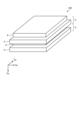
- FIG. 1A is a side view showing an example of a lighting device according to an embodiment
- FIG. FIG. 1B is a perspective view showing an example of the light control device according to the embodiment
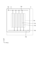
- FIG. 2 is a schematic plan view of the first substrate viewed from the Dz direction.
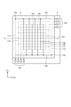
- FIG. 3 is a schematic plan view of the second substrate viewed from the Dz direction.
- FIG. 4 is a perspective view of a liquid crystal cell in which the first substrate and the second substrate are stacked in the Dz direction.
- FIG. 5 is a cross-sectional view taken along line A-A' shown in FIG.
- FIG. 6A is a diagram showing the rubbing direction of the alignment film of the first substrate.
- FIG. 6B is a diagram showing the rubbing direction of the alignment film of the second substrate.
- FIG. 6A is a diagram showing the rubbing direction of the alignment film of the first substrate.
- FIG. 6B is a diagram showing the rubbing direction of the alignment film of the second substrate.
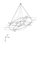
- FIG. 7 is a conceptual diagram conceptually explaining the light distribution angle of the lighting device according to the embodiment.
- FIG. 8 is a schematic diagram illustrating an example of a configuration of a lighting control system according to the embodiment;
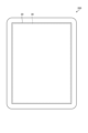
- FIG. 9 is an external view showing an example of the control device according to the embodiment;
- FIG. 10 is a conceptual diagram showing an example of a touch detection area in a touch sensor.
- 11 is a diagram illustrating an example of a control block configuration for adjusting the first data to be transmitted to the lighting device in the control device according to the first embodiment;
- FIG. FIG. 12 is a conceptual diagram showing an example of a first data adjustment method according to the first embodiment.
- 13A is a conceptual diagram showing a first display mode for adjusting first data in the control device according to the first embodiment;
- FIG. 13B is a conceptual diagram showing a second display mode for adjusting first data in the control device according to the first embodiment
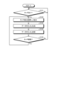
- FIG. 14 is a flowchart illustrating an example of first data generation processing in the control device according to the first embodiment
- FIG. 15 is a diagram illustrating an example of a control block configuration for controlling a light control device in the lighting device according to the first embodiment
- FIG. 16A is a diagram showing a first example of a lookup table showing correspondence between first data and second data.
- FIG. 16B is a diagram showing a second example of a lookup table showing correspondence between first data and second data.
- FIG. 16C is a diagram showing a third example of a lookup table showing correspondence between first data and second data.
- FIG. 17 is a flowchart illustrating an example of light distribution angle control processing in the lighting device according to the first embodiment
- FIG. FIG. 18 is a schematic diagram showing the relationship between the light distribution angle controlled by the lighting device according to the second embodiment and the light irradiation range.
- 19 is a flowchart illustrating an example of light distribution angle control processing in the lighting device according to the second embodiment
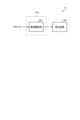
- FIG. 20 is a diagram illustrating an example of a control block configuration for adjusting the second data to be transmitted to the lighting device in the control device according to the third embodiment
- FIG. 21 is a diagram illustrating an example of a control block configuration for controlling a light control device in the lighting device according to the third embodiment
- FIG. 1A is a side view showing an example of the lighting device according to the embodiment.
- FIG. 1B is a perspective view showing an example of the light control device according to the embodiment;
- the illumination device 1 includes a light source 4, a reflector 4a, and a dimming device 100.
- the light control device 100 includes a first liquid crystal cell 2 and a second liquid crystal cell 3 .
- the light source 4 is composed of, for example, a light emitting diode (LED: Light Emitting Diode).
- the reflector 4 a is a component that collects the light from the light source 4 to the light control device 100 .
- the Dz direction indicates the irradiation direction of light from the light source 4 and the reflector 4a.
- the light control device 100 is configured by stacking a first liquid crystal cell 2 and a second liquid crystal cell 3 in the Dz direction.
- one direction of the plane parallel to the lamination plane of the first liquid crystal cell 2 and the second liquid crystal cell 3 orthogonal to the Dz direction is the Dx direction
- the direction orthogonal to both the Dx direction and the Dz direction is the Dy direction. It is said that
- the first liquid crystal cell 2 and the second liquid crystal cell 3 have the same configuration.
- the first liquid crystal cell 2 is a liquid crystal cell for p-wave polarized light.
- the second liquid crystal cell 3 is a liquid crystal cell for s-wave polarization.
- the first liquid crystal cell 2 may be a liquid crystal cell for s-wave polarization
- the second liquid crystal cell 3 may be a liquid crystal cell for p-wave polarization. It is sufficient that one of the first liquid crystal cell 2 and the second liquid crystal cell 3 is a liquid crystal cell for p-wave polarization and the other is a liquid crystal cell for s-wave polarization.
- FIG. 2 is a schematic plan view of the first substrate viewed from the Dz direction.
- FIG. 3 is a schematic plan view of the second substrate viewed from the Dz direction.
- FIG. 4 is a perspective view of a liquid crystal cell in which the first substrate and the second substrate are stacked in the Dz direction.
- FIG. 5 is a cross-sectional view taken along line A-A' shown in FIG.
- the first liquid crystal cell 2 and the second liquid crystal cell 3 are provided with a liquid crystal layer 8 between a first substrate 5 and a second substrate 6, the periphery of which is sealed with a sealing material 7. ing.
- the liquid crystal layer 8 modulates light passing through the liquid crystal layer 8 according to the state of the electric field.
- the liquid crystal layer 8 may employ a horizontal electric field mode such as FFS (fringe field switching), which is a form of IPS (in-plane switching), or may use a vertical electric field mode.
- FFS frequency field switching
- IPS in-plane switching
- liquid crystals of various modes such as TN (Twisted Nematic), VA (Vertical Alignment), and ECB (Electrically Controlled Birefringence) may be used. is not limited by
- the drive electrodes 10 on the first substrate 5 extend in the Dx direction.
- the drive electrodes 13 on the second substrate 6 extend in the Dy direction.
- the drive electrode 10 and the drive electrode 13 are translucent electrodes made of a translucent conductive material (translucent conductive oxide) such as ITO (Indium Tin Oxide).
- the first substrate 5 and the second substrate 6 are translucent substrates such as glass or resin.
- the first metal wiring 11 and the second metal wiring 14 are made of at least one metal material selected from aluminum (Al), copper (Cu), silver (Ag), molybdenum (Mo), and alloys thereof. Also, the first metal wiring 11 and the second metal wiring 14 may be a laminate obtained by laminating a plurality of metal materials using one or more of these metal materials. At least one metal material of aluminum (Al), copper (Cu), silver (Ag), molybdenum (Mo), or alloys thereof has a lower resistance than translucent conductive oxides such as ITO.
- the metal wiring 11a of the first substrate 5 and the metal wiring 14a of the second substrate 6 are connected by a conducting portion 15a such as a via, for example. Also, the metal wiring 11d of the first substrate 5 and the metal wiring 14b of the second substrate 6 are connected by a conducting portion 15b such as a via, for example.
- connection terminal portion 16a to be connected to a flexible printed circuit board (FPC: Flexible Printed Circuits) (not shown) is provided on the first substrate 5 and does not overlap with the second substrate 6 in the Dz direction. , 16b are provided.
- the connection terminal portions 16a and 16b have four connection terminals corresponding to the metal wirings 11a, 11b, 11c and 11d, respectively.
- connection terminal portions 16 a and 16 b are provided in the wiring layer of the first substrate 5 .
- the first liquid crystal cell 2 and the second liquid crystal cell 3 are connected to the drive electrodes 10a and 10b on the first substrate 5 and the drive electrode 13a on the second substrate 6 from the FPC connected to the connection terminal portion 16a or the connection terminal portion 16b. , 13b is supplied.
- connection terminal portions 16a and 16b may be simply referred to as "connection terminal portion 16".
- the first substrate 5 and the second substrate 6 are overlapped in the Dz direction (light irradiation direction).
- a plurality of drive electrodes 10 on the substrate 5 and a plurality of drive electrodes 13 on the second substrate 6 intersect.
- driving voltages are supplied to the plurality of driving electrodes 10 on the first substrate 5 and the plurality of driving electrodes 13 on the second substrate 6, respectively.
- the alignment direction of the liquid crystal molecules 17 of the liquid crystal layer 8 can be controlled.
- a region in which the alignment direction of the liquid crystal molecules 17 of the liquid crystal layer 8 can be controlled is referred to as a "light control region AA".
- the refractive index distribution of the liquid crystal layer 8 in this dimming area AA By changing the refractive index distribution of the liquid crystal layer 8 in this dimming area AA, it becomes possible to control light passing through the dimming area AA of the first liquid crystal cell 2 and the second liquid crystal cell 3 .
- the area where the liquid crystal layer 8 is sealed with the sealing material 7 is called a "peripheral area GA" (see FIG. 5).
- the drive electrodes 10 (the drive electrodes 10a in FIG. 5) are covered with the alignment film 18.
- the driving electrodes 13 (the driving electrodes 13 a and 13 b in FIG. 5 ) are covered with the alignment film 19 in the light control region of the second substrate 6 .
- the orientation film 18 and the orientation film 19 have different rubbing directions.
- FIG. 6A is a diagram showing the rubbing direction of the alignment film of the first substrate.
- FIG. 6B is a diagram showing the rubbing direction of the alignment film of the second substrate.
- the rubbing direction of the alignment film 18 of the first substrate and the rubbing direction of the alignment film 19 of the second substrate are directions that cross each other in plan view.
- the rubbing direction of the alignment film 18 of the first substrate 5 shown in FIG. 6A is orthogonal to the extending direction of the drive electrodes 10a and 10b.
- the rubbing direction of the alignment film 19 of the second substrate 6 shown in FIG. 6B is perpendicular to the extending direction of the drive electrodes 13a and 13b.
- a structure in which one first liquid crystal cell 2 and one second liquid crystal cell 3 are stacked is described, but the structure is not limited to this structure.
- a configuration having a plurality of combinations in which the liquid crystal cells 3 are laminated may be used.
- a configuration having two combinations in which the first liquid crystal cell 2 and the second liquid crystal cell 3 are stacked that is, a configuration having two liquid crystal cells for p-wave polarization and two liquid crystal cells for s-wave polarization. Also good.
- the light distribution angle of the light emitted from the light source 4 is controlled by driving voltage control of the first liquid crystal cell 2 and the second liquid crystal cell 3 .
- the light distribution angle of the lighting device 1 to be controlled in the present disclosure will be described below with reference to FIG. 7 .
- FIG. 7 is a conceptual diagram conceptually explaining the light distribution angle of the lighting device according to the embodiment.
- the illumination device 1 is assumed to be a point light source A, and the irradiation range of light on a virtual plane xy perpendicular to the Dz direction is shown.
- FIG. 7 shows an example in which the illumination device 1 is regarded as a point light source A. Since it is configured to control transmitted light, the illuminance of the light decreases around the irradiation range. In addition, the outline of the irradiation range becomes unclear due to the diffraction phenomenon of light or the like.
- the alignment direction of the liquid crystal molecules 17 of the liquid crystal layer 8 of the first liquid crystal cell 2 changes according to the drive voltage applied to the drive electrode 10 and the drive electrode 13 of the first liquid crystal cell 2,
- the light distribution angle in the Dx direction changes.
- the minimum light distribution angle in the Dx direction is 0[%] and the maximum light distribution angle in the Dx direction is 100[%].
- the alignment direction of the liquid crystal molecules 17 of the liquid crystal layer 8 of the second liquid crystal cell 3 changes, and the Dy direction changes.
- Light distribution angle changes.
- the minimum light distribution angle in the Dy direction is 0[%]
- the maximum light distribution angle in the Dy direction is 100[%].
- a illustrates an irradiation range when both the light distribution angle in the Dx direction and the light distribution angle in the Dy direction are 100[%].
- b shown in FIG. 7 illustrates an irradiation range when the light distribution angle in the Dx direction is 100[%] and the light distribution angle in the Dy direction is 30[%].
- c shown in FIG. 7 illustrates an irradiation range when the light distribution angle in the Dx direction is 30[%] and the light distribution angle in the Dy direction is 100[%].
- d shown in FIG. 7 illustrates an irradiation range when both the light distribution angle in the Dx direction and the light distribution angle in the Dy direction are 30[%].
- the illumination device 1 having the configuration described above, by controlling the driving voltages of the first liquid crystal cell 2 and the second liquid crystal cell 3, the light distribution angles of the light in the Dx direction and the Dy direction can be controlled. can. Thereby, the irradiation range of the light of the lighting device 1 can be changed.
- FIG. 8 is a schematic diagram showing an example of the configuration of the lighting control system according to the embodiment.
- the lighting control system includes lighting device 1 and control device 200 .
- the control device 200 is exemplified by a mobile communication terminal device such as a smart phone or a tablet, for example.
- the communication means 300 is, for example, wireless communication means such as Bluetooth (registered trademark) or WiFi (registered trademark).
- the lighting device 1 and the control device 200 may communicate wirelessly via a predetermined network such as a mobile communication network, for example.
- the lighting device 1 and the control device 200 may be connected by wire to perform wired communication.
- FIG. 9 is an external view showing an example of the control device according to the embodiment.
- the control device 200 is a display device with a touch detection function in which the display panel 20 and the touch sensor 30 are integrated.
- the display panel 20 is a so-called in-cell type or hybrid type device in which the touch sensor 30 is incorporated and integrated. Integrating the touch sensor 30 into the display panel 20 means, for example, that some members such as the substrate and electrodes used as the display panel 20 and some members such as the substrate and electrodes used as the touch sensor 30 It includes also serving as a member of
- the display panel 20 may be a so-called on-cell type device in which the touch sensor 30 is mounted on the display device.
- the display panel 20 for example, a liquid crystal display panel using a liquid crystal display element is exemplified.
- the display panel 20 is not limited to this, and may be, for example, an organic EL display panel (OLED: Organic Light Emitting Diode) or an inorganic EL display panel (micro LED, mini LED).
- OLED Organic Light Emitting Diode
- micro LED mini LED
- the touch sensor 30 is a capacitive touch sensor.
- the touch sensor 30 is not limited to this, and may be, for example, a resistive touch sensor, an ultrasonic touch sensor, or an optical touch sensor.
- FIG. 10 is a conceptual diagram showing an example of a touch detection area in a touch sensor.
- a plurality of detection elements 31 are provided in the detection area FA of the touch sensor 30 .
- the multiple detection elements 31 are arranged in a matrix in the X direction (first direction) and the Y direction (second direction) perpendicular to the X direction within the detection area FA of the touch sensor 30 .
- the touch sensor 30 has a detection area FA overlapping the plurality of detection elements 31 arranged in the X direction (first direction) and the Y direction (second direction).
- (Embodiment 1) 11 is a diagram illustrating an example of a control block configuration for adjusting the first data to be transmitted to the lighting device in the control device according to the first embodiment;
- FIG. 1 is a diagram illustrating an example of a control block configuration for adjusting the first data to be transmitted to the lighting device in the control device according to the first embodiment;
- the control device 200 includes a detection device 210 and a processing device 220.
- the detection device 210 includes a touch sensor 30 , a detection section 211 and a coordinate extraction section 212 .
- the processing device 220 includes a first data generation section 221 and a storage section 223 .
- the detection unit 211 and the coordinate extraction unit 212 of the detection device 210 are configured by detection ICs, for example.
- the processing device 220 is, for example, a CPU (Central Processing Unit), RAM (Random Access Memory), EEPROM (Electrically Erasable Programmable Read Only Memory), ROM (Read Only Memory), etc. of a smartphone or tablet that constitutes the control device 200. Configured.
- the detection unit 211 is a circuit that detects whether or not the touch sensor 30 is touched based on detection signals output from the detection elements 31 of the touch sensor 30 .
- the coordinate extraction unit 212 is a logic circuit that obtains the coordinates of the touch detection position when the detection unit 211 detects a touch.
- the first data generation unit 221 generates first data in the X direction and first data in the Y direction based on the touch detection position extracted by the coordinate extraction unit 212 .
- the first data generation unit 221 is, for example, a configuration unit realized by a CPU of a smartphone, tablet, or the like that configures the control device 200 .
- the storage unit 223 is composed of, for example, the RAM, EEPROM, ROM, etc. of a smartphone, tablet, etc. that constitute the control device 200 .
- the storage unit 223 stores first data corresponding to the coordinates of the touch detection position extracted by the coordinate extraction unit 212, for example.
- FIG. 12 is a conceptual diagram showing an example of a first data adjustment method according to the first embodiment.
- a data adjustment area TA is provided within the detection area FA of the touch sensor 30 .
- the horizontal axis of the data adjustment area TA indicates the coordinate axis in the X direction (first direction) and corresponds to the Dx direction in the lighting device 1 .
- the vertical axis of the data adjustment area TA indicates the coordinate axis in the Y direction (second direction) and corresponds to the Dy direction in the illumination device 1 .
- the data adjustment area TA may be provided within the detection area FA of the touch sensor 30, and the data adjustment area TA may be the entire area of the detection area FA.
- the first data in the X direction and the first data in the Y direction are respectively discrete values obtained by normalizing the information on the light distribution angle controlled by the lighting device 1 . That is, in the present embodiment, the first data generator 221 generates the first data R (Rx, Ry) using the information on the light distribution angle controlled by the lighting device 1 as a control parameter for the control device 200 .
- the first data R (Rx, Ry) generated by the first data generator 221 in this embodiment is also referred to as "first light distribution angle information”.
- the first data Rx in the X direction and the first data Ry in the Y direction each define values corresponding to the coordinates of the touch detection position detected in the data adjustment area TA.
- the first data Rx in the X direction and the first data Ry in the Y direction can take values from "0" to "100".
- the circle indicated by the dashed line in FIG. 12A indicates the trajectory of the coordinates of the position where the first data Rx in the X direction is "30" and the first data Ry in the Y direction is "30".
- the locus of the coordinates of the position where the first data Rx of is "100” and the first data Ry in the Y direction is "100".
- the trajectory of the coordinates of the position where the first data Ry of the direction is "50" is shown.
- FIG. 12 shows an example in which the coordinates of the touch detection position are moved from position A to position B within the data adjustment area TA by the coordinate extraction unit 212 .
- the first data generation unit 221 generates the coordinates of the touch detection position output from the coordinate extraction unit 212 in time series ( First data R (Rx, Ry) corresponding to x, y) is generated.
- First data R (Rx, Ry) corresponding to x, y
- k is a coefficient determined by the number of sensing elements 31 in the data adjustment area TA.
- the first data changes by one step when the coordinates of the touch detection position move by four. That is, the amount of change in the first data R (Rx, Ry) is proportional to the amount of movement of the coordinates (x, y) of the touch detection position.
- the control device 200 sequentially transmits the first data R (Rx, Ry) generated by the first data generating section 221 to the lighting device 1 .
- FIG. 13A is a conceptual diagram showing a first display mode for adjusting first data in the control device according to Embodiment 1.
- FIG. 13B is a conceptual diagram showing a second display mode for adjusting first data in the control device according to the first embodiment;
- the display panel 20 is provided with a display area DA that overlaps the detection area FA of the touch sensor 30 shown in FIG. 9 in plan view.
- FIG. 13A shows a mode in which the trajectory of the coordinates of the position corresponding to the first data R (Rx, Ry) on the data adjustment area TA is displayed as the schematic shape image 23 of the irradiation range.
- this first display mode for example, by tapping the position A on the outline shape image 23 of the irradiation range and swiping to the position B, the first data Rx in the X direction and the first data Ry in the Y direction are simultaneously adjusted. do.
- FIG. 13B shows a mode in which a slide bar 24a for adjusting the first data Rx in the X direction and a slide bar 24b for adjusting the first data Ry in the Y direction are displayed on the data adjustment area TA.
- the first data Rx is adjusted by tapping the slide bar 24a and swiping in the X direction
- the first data Ry is adjusted by tapping the slide bar 24b and swiping in the Y direction.
- the mode of adjusting the first data is not limited to the mode described above, and may be, for example, a mode in which a physical slider is provided in the control device 200.
- FIG. 14 is a flowchart showing an example of first data generation processing in the control device according to the first embodiment.
- the detection unit 211 detects whether or not there is a touch within the data adjustment area TA of the touch sensor 30 (step S101).
- the coordinate extraction unit 212 extracts the coordinates (x, y) of the touch detection position (step S102).
- the first data generation unit 221 generates first data R (Rx, Ry) corresponding to the coordinates (x, y) of the touch detection position (step S103). Specifically, the first data generation unit 221 reads from the storage unit 223 the first data R (Rx, Ry) corresponding to the coordinates (x, y) of the touch detection position extracted by the coordinate extraction unit 212 .
- the control device 200 transmits the first data R (Rx, Ry) generated by the first data generating section 221 to the lighting device 1 via the communication means 300 (step S104).
- the detection unit 211 detects whether or not the touch within the data adjustment area TA of the touch sensor 30 continues (step S105).
- step S101 If the touch is not detected in step S101 (step S101; No), or if the touch is not continued in step S105 (step S105; No), the process returns to step S101 to repeat the same process.
- step S105 When the touch in the data adjustment area TA of the touch sensor 30 continues (step S105; Yes), the process returns to step S102, and the processes after step S102 are repeatedly executed.
- the lighting device 1 changes the light distribution angles of the light in the Dx direction and the Dy direction according to the first data R (Rx, Ry) transmitted from the control device 200 .
- the configuration and operation for controlling the light distribution angle of the lighting device according to the first embodiment will be described below.
- FIG. 15 is a diagram showing an example of a control block configuration for controlling the light control device in the lighting device according to the first embodiment.
- control unit 110 of the lighting device 1 according to Embodiment 1 includes a second data generation unit 111, an electrode driving unit 112, and a storage unit 113.
- the second data generation unit 111 Based on the first light distribution angle information (first data R (Rx, Ry)) received from the control device 200, the second data generation unit 111 generates the second data Ax in the Dx direction and the second data Ax in the Dy direction of the lighting device 1. 2 Generate data Ay.
- the second data Ax in the Dx direction and the second data Ay in the Dy direction generated by the second data generation unit 111 are obtained by normalizing the information on the light distribution angle controlled in the lighting device 1. Discrete values.
- the second data A (Ax, Ay) generated by the second data generator 111 in this embodiment is also referred to as "second light distribution angle information”.
- the electrode driving unit 112 controls the first liquid crystal cell 2 and the second liquid crystal cell 2 of the light control device 100.
- a drive voltage is supplied to each of the drive electrodes 10 and 13 of the cell 3 .
- the storage unit 113 stores a lookup table showing the correspondence between the first data R (Rx, Ry) and the second data A (Ax, Ay).
- Second data generation unit 111 refers to the lookup table stored in storage unit 113 and generates second data A (Ax, Ay) corresponding to first data R (Rx, Ry) received from control device 200. It reads out and outputs the read second data A (Ax, Ay) to the electrode driving section 112 as the second light distribution angle information.
- FIG. 16A is a diagram showing a first example of a lookup table showing correspondence between first data and second data.
- FIG. 16B is a diagram showing a second example of a lookup table showing correspondence between first data and second data.
- FIG. 16C is a diagram showing a third example of a lookup table showing correspondence between first data and second data.
- the horizontal axis indicates the first data R (Rx, Ry), and the vertical axis indicates the second data A (Ax, Ay).
- the second data Ax in the Dx direction and the second data Ay in the Dy direction can each take values from “0" to "100".
- the maximum value (100) of the second data Ax in the Dx direction and the second data Ay in the Dy direction corresponds to the maximum value of the light distribution angle control range in the illumination device 1 (dimmer 100).
- 16C indicates that the correspondence between the first data R (Rx, Ry) and the second data A (Ax, Ay) is linear, and the maximum value of the first data R (Rx, Ry) ( 100) shows an example in which the second data A (Ax, Ay) is the maximum value (100).
- the slope of the second data A (Ax, Ay) with respect to the first data R (Rx, Ry) is the range less than R1 of the first data R (Rx, Ry) and different in range.
- the slope of the second data A (Ax, Ay) with respect to the first data R (Rx, Ry) in the range less than R1 of the first data R (Rx, Ry) is the first data R (Rx, Ry ) is smaller than the slope of the second data A (Ax, Ay) with respect to the first data R (Rx, Ry) in the range of R1 or more.
- 0 of the second light distribution angle information (second data A (Ax, Ay)) corresponding to the range from 0 to R1 of the first data R (Rx, Ry) to A1, higher than the other range (the range of A1 to 100 of the second data A (Ax, Ay) corresponding to the range of R1 to 100 of the first data R (Rx, Ry))
- Accurate light distribution angle control can be performed.
- the adjustment accuracy of the irradiation range of the illumination device 1 with respect to the amount of change in the touch detection position on the data adjustment range TA of the control device 200. can be raised.
- the gradient of the second data A (Ax, Ay) with respect to the first data R (Rx, Ry) is The range is different from the range of R1 or more and less than R2.
- the slope of the second data A (Ax, Ay) with respect to the first data R (Rx, Ry) in the range from R1 to R2 of the first data R (Rx, Ry) is the first data R (Rx , Ry) is smaller than the slope of the second data A (Ax, Ay) with respect to the first data R (Rx, Ry) in the range less than R1 and in the range greater than or equal to R2.
- the adjustment accuracy of the illumination range of the illumination device 1 with respect to the amount of change in the touch detection position on the data adjustment range TA of the control device 200. can be raised.
- the slope of the second data A (Ax, Ay) with respect to the first data R (Rx, Ry) is constant over the entire range of the first data R (Rx, Ry).
- the second data A (Ax, Ay) increases linearly as the first data R (Rx, Ry) increases over the entire range of the first data R (Rx, Ry).
- the maximum value A1 of the second data A (Ax, Ay) is smaller than the maximum value of the light distribution angle control range in the illumination device 1 (dimmer 100).
- the accuracy is higher than the example shown by the broken line.
- Light distribution angle control can be performed.
- the amount of change in the touch detection position on the data adjustment range TA of the control device 200 is greater than the example shown by the dashed line. Adjustment accuracy can be improved.
- the lookup table stored in the storage unit 113 is not limited to the forms shown in FIGS. 16A, 16B, and 16C.
- the lookup table shown in FIG. 16A and the lookup table shown in FIG. 16C may be combined, or the lookup table shown in FIG. 16B and the lookup table shown in FIG. 16C may be combined. It can be.
- FIG. 16A and 16B illustrate a mode in which the second data A (Ax, Ay) linearly increases as the first data R (Rx, Ry) increases except at the inflection point. It may be in a curved form including.
- FIG. 16C illustrates a mode in which the correspondence relationship between the first data R (Rx, Ry) and the second data A (Ax, Ay) is linear over the entire range. ) may increase the rate of increase of the second data A (Ax, Ay), or as the first data R (Rx, Ry) increases, the second data A (Ax, Ay) may be reduced in rate of increase.
- the correspondence information indicating the correspondence relationship between the first data R (Rx, Ry) and the second data A (Ax, Ay) is limited to lookup tables as shown in FIGS. 16A, 16B, and 16C. Instead, for example, a function defining the correspondence relationship between the first data R (Rx, Ry) and the second data A (Ax, Ay) may be stored in the storage unit 113. The second data A (Ax, Ay) corresponding to the data R (Rx, Ry) may be stored as data.
- FIG. 17 is a flowchart showing an example of light distribution angle control processing in the lighting device according to the first embodiment.
- the second data generation unit 111 determines whether or not the first light distribution angle information has been received from the control device 200 (step S201).
- step S201 If the first light distribution angle information has not been received in step S201 (step S201; No), the process of step S201 is repeated.
- Step S201 When the first light distribution angle information is received (Step S201; Yes), the second data generation unit 111 generates the second data A (Ax, Ay) corresponding to the first data R (Rx, Ry) from the storage unit 113. It is read (step S202), output to the electrode drive unit 112 as second light distribution angle information (step S203), and returns to the process of step S201.
- the lighting device 1 uses the first data R (Rx, Ry) transmitted from the control device 200 and the second data A (Ax, Ay) used for controlling the light control device 100. , and generates second data A (Ax, Ay) obtained by correcting the first data R (Rx, Ry) based on the correspondence information to generate the first data A (Ax, Ay) of the light control device 100 A drive voltage is supplied to the drive electrodes 10 and 13 of the liquid crystal cell 2 and the second liquid crystal cell 3 .
- control device 200 can arbitrarily set a range in which the adjustment accuracy of the light irradiation range is desired to be increased, and the highly convenient lighting device 1 can be obtained.
- FIG. 18 is a schematic diagram showing the relationship between the light distribution angle controlled by the lighting device according to the second embodiment and the light irradiation range.
- the lighting device 1 is assumed to be a point light source A, and a light irradiation range d on virtual planes a, b, and c perpendicular to the Dz direction is shown.
- the light irradiation range (beam diameter determined by the light distribution angle ⁇ ) d differs depending on the distance h from the lighting device 1 .
- the light distribution angle ⁇ in this case is given by the following equation (3).
- the first data in the X direction and the first data in the Y direction are discrete values obtained by normalizing the irradiation range information in which the distance from the illumination device 1 to the object to be irradiated with light is determined. . That is, in the present embodiment, the first data generation unit 221 uses the information of the irradiation range in which the distance from the lighting device 1 to the light irradiation object is determined as the control parameter in the control device 200 as the first data R (Rx , Ry).
- the first data R (Rx, Ry) generated by the first data generator 221 in this embodiment is also referred to as "irradiation range information”.
- the second data A (Ax, Ay) generated by the second data generator 111 in this embodiment is also referred to as "light distribution angle information”.
- the second data generation unit 111 generates second data Ax in the Dx direction of the lighting device 1 and Generate second data Ay in the Dy direction.
- the lookup table applied in the present embodiment may be a mode that reflects the above equation (3) with respect to the lookup tables shown in FIGS. 16A, 16B, and 16C described in the first embodiment.
- FIG. 19 is a flowchart showing an example of light distribution angle control processing in the lighting device according to the second embodiment.
- the second data generation unit 111 determines whether or not irradiation range information has been received from the control device 200 (step S301).
- step S301 If the irradiation range information has not been received in step S301 (step S301; No), the process of step S301 is repeatedly executed.
- the second data generation unit 111 reads the second data A (Ax, Ay) corresponding to the first data R (Rx, Ry) from the storage unit 113 (step S302), output to the electrode drive unit 112 as light distribution angle information (step S303), and return to the process of step S301.
- control device 200 can arbitrarily set a range in which the adjustment accuracy of the light irradiation range is desired to be increased, and the highly convenient lighting device 1 can be obtained.
- FIG. 3 is a diagram illustrating an example of a control block configuration for adjusting the second data to be transmitted to the lighting device in the control device according to the third embodiment
- FIG. 21 is a diagram illustrating an example of a control block configuration for controlling a light control device in the lighting device according to the third embodiment
- FIG. 3 is a diagram illustrating an example of a control block configuration for controlling a light control device in the lighting device according to the third embodiment
- the processing device 220a of the control device 200a according to Embodiment 3 has the configuration provided in the control unit 110 of the lighting device 1 in Embodiments 1 and 2.
- a second data generator 222 corresponding to the second data generator 111 is provided.
- the storage unit 223a stores a lookup table showing the correspondence between the first data R (Rx, Ry) and the second data A (Ax, Ay).
- the second data generation unit 222 refers to the lookup table stored in the storage unit 223a to obtain second data A (Ax) corresponding to the first data R (Rx, Ry) generated by the first data generation unit 221. , Ay), and transmits the read second data A (Ax, Ay) to the illumination device 1a.
- the first data R may be a discrete value obtained by normalizing the information of the light distribution angle controlled by the lighting device 1, as in the first embodiment, or as in the second embodiment, It may be a discrete value obtained by normalizing the irradiation range information in which the distance from the illumination device 1 to the object to be irradiated with light is determined.
- the control device 200a establishes the correspondence between the first data R (Rx, Ry) generated by the first data generation unit 221 and the second data A (Ax, Ay) used for controlling the light control device 100. Correspondence information indicating the relationship is held, and based on the correspondence information, the second data A (Ax, Ay) is generated by correcting the first data R (Rx, Ry) and transmitted to the lighting device 1a. Based on the second data A (Ax, Ay) transmitted from the control device 200a, the control unit 110a of the illumination device 1a controls the driving electrodes 10, 10 of the first liquid crystal cell 2 and the second liquid crystal cell 3 of the light control device 100. 13 is supplied with a drive voltage.
- control device 200a can arbitrarily set a range in which the adjustment accuracy of the light irradiation range is desired to be increased, and a highly convenient illumination device 1a can be obtained.
- Reference Signs List 1 1a lighting device 2 first liquid crystal cell 3 second liquid crystal cell 4 light source 5 first substrate 6 second substrate 7 sealing material 8 liquid crystal layer 9 base material 10, 10a, 10b drive electrode 11 first metal wiring 11a, 11b , 11c, 11d metal wiring 12 base material 13, 13a, 13b drive electrode 14 second metal wiring 14a, 14b metal wiring 15a, 15b conduction part 16a, 16b connection terminal part 17 liquid crystal molecule 18 alignment film 19 alignment film 20 display panel 23 Outline shape image (irradiation range) 24a, 24b slide bar 30 touch sensor 31 detection element 100 light control device 110, 110a control unit 111 second data generation unit 112 electrode drive unit 113 storage unit 200, 200a control device 210 detection device 211 detection unit 212 coordinate extraction unit 220, 220a processing device 221 first data generation unit 222 second data generation unit 223, 223a storage unit 300 communication means AA dimming area DA display area FA detection area GA peripheral area TA data adjustment area
Landscapes
- Physics & Mathematics (AREA)
- Engineering & Computer Science (AREA)
- Nonlinear Science (AREA)
- Chemical & Material Sciences (AREA)
- Crystallography & Structural Chemistry (AREA)
- General Physics & Mathematics (AREA)
- Optics & Photonics (AREA)
- Computer Networks & Wireless Communication (AREA)
- Multimedia (AREA)
- General Engineering & Computer Science (AREA)
- Mathematical Physics (AREA)
- Circuit Arrangement For Electric Light Sources In General (AREA)
Abstract
Description
図11は、実施形態1に係る制御装置において、照明装置に送信する第1データを調整する制御ブロック構成の一例を示す図である。
実施形態1では、照明装置1において制御される配光角の情報を制御装置200における制御パラメータとして第1データR(Rx,Ry)を生成する例を示したが、実施形態2では、照明装置1の光の照射範囲の情報を制御装置200における制御パラメータとする例について説明する。
図20は、実施形態3に係る制御装置において、照明装置に送信する第2データを調整する制御ブロック構成の一例を示す図である。図21は、実施形態3に係る照明装置において、調光装置を制御する制御ブロック構成の一例を示す図である。
2 第1液晶セル
3 第2液晶セル
4 光源
5 第1基板
6 第2基板
7 封止材
8 液晶層
9 基材
10,10a,10b 駆動電極
11 第1金属配線
11a,11b,11c,11d 金属配線
12 基材
13,13a,13b 駆動電極
14 第2金属配線
14a,14b 金属配線
15a,15b 導通部
16a,16b 接続端子部
17 液晶分子
18 配向膜
19 配向膜
20 表示パネル
23 概略形状イメージ(照射範囲)
24a,24b スライドバー
30 タッチセンサ
31 検出素子
100 調光装置
110,110a 制御部
111 第2データ生成部
112 電極駆動部
113 記憶部
200,200a 制御装置
210 検出装置
211 検出部
212 座標抽出部
220,220a 処理装置
221 第1データ生成部
222 第2データ生成部
223,223a 記憶部
300 通信手段
AA 調光領域
DA 表示領域
FA 検出領域
GA 周辺領域
TA データ調整領域
Claims (15)
- 光源と、
前記光源から照射される光の配光角を制御する調光装置と、
前記調光装置を制御する制御部と、
を備え、
前記制御部は、
制御装置から入力される第1データと前記配光角の制御に用いる第2データとの対応関係を示す対応情報を保持する記憶部と、
前記対応情報に基づき、前記第1データを補正した第2データを生成するデータ生成部と、
前記第2データに基づき、前記調光装置を駆動する駆動部と、
を備える、
照明装置。 - 前記第1データに対する第2データの傾きは、前記第1データの所定値未満の範囲と前記所定値以上の範囲とで異なっている、
請求項1に記載の照明装置。 - 前記第2データの最大値に基づき前記調光装置において制御される配光角は、前記調光装置における配光角の制御範囲の最大値よりも小さい、
請求項1又は2に記載の照明装置。 - 前記第1データは、前記調光装置における配光角の情報を正規化した離散値である、
請求項1から3の何れか一項に記載の照明装置。 - 前記第1データは、照射対象物までの距離で定められた照射範囲の情報を正規化した離散値である、
請求項1から3の何れか一項に記載の照明装置。 - 光源から照射される光の配光角を制御可能な照明装置と、前記照明装置を制御する制御装置と、を備えた照明制御システムであって、
前記制御装置は、
タッチセンサと、
前記タッチセンサにおけるタッチ検出位置を抽出する検出部と、
前記タッチ検出位置に応じた第1データを生成する第1データ生成部と、
を備え、
前記照明装置は、
前記配光角を制御する調光装置と、
前記調光装置を制御する制御部と、
を備え、
前記制御部は、
前記第1データと前記配光角の制御に用いる第2データとの対応関係を示す対応情報を保持する記憶部と、
前記対応情報に基づき、前記第1データを補正した第2データを生成する第2データ生成部と、
前記第2データに基づき、前記調光装置を駆動する駆動部と、
を備える、
照明制御システム。 - 前記第1データに対する第2データの傾きは、前記第1データの所定値未満の範囲と前記所定値以上の範囲とで異なっている、
請求項6に記載の照明制御システム。 - 前記第2データの最大値に基づき前記調光装置において制御される配光角は、前記調光装置における配光角の制御範囲の最大値よりも小さい、
請求項6又は7に記載の照明制御システム。 - 前記第1データは、前記調光装置における配光角を正規化した離散値である、
請求項6から8の何れか一項に記載の照明制御システム。 - 前記第1データは、照射対象物までの距離に基づき定められた照射範囲の情報を正規化した離散値である、
請求項6から8の何れか一項に記載の照明制御システム。 - 光源から照射される光の配光角を制御可能な照明装置と、前記照明装置を制御する制御装置と、を備えた照明制御システムであって、
前記制御装置は、
タッチセンサと、
前記タッチセンサにおけるタッチ検出位置を抽出する検出部と、
前記タッチ検出位置に応じた第1データを生成する第1データ生成部と、
前記第1データと前記配光角の制御に用いる第2データとの対応関係を示す対応情報を保持する記憶部と、
前記対応情報に基づき、前記第1データを補正した第2データを生成する第2データ生成部と、
を備え、
前記照明装置は、
前記配光角を制御する調光装置と、
前記調光装置を制御する制御部と、
を備え、
前記制御部は、
前記第2データに基づき、前記調光装置を駆動する駆動部を備える、
照明制御システム。 - 前記第1データに対する第2データの傾きは、前記第1データの所定値未満の範囲と前記所定値以上の範囲とで異なっている、
請求項11に記載の照明制御システム。 - 前記第2データの最大値に基づき前記調光装置において制御される配光角は、前記調光装置における配光角の制御範囲の最大値よりも小さい、
請求項11又は12に記載の照明制御システム。 - 前記第1データは、前記調光装置における配光角を正規化した離散値である、
請求項11から13の何れか一項に記載の照明制御システム。 - 前記第1データは、照射対象物までの距離に基づき定められた照射範囲の情報を正規化した離散値である、
請求項11から13の何れか一項に記載の照明制御システム。
Priority Applications (3)
| Application Number | Priority Date | Filing Date | Title |
|---|---|---|---|
| CN202280089752.2A CN118575581A (zh) | 2022-01-26 | 2022-12-23 | 照明装置以及照明控制系统 |
| JP2023576717A JPWO2023145347A1 (ja) | 2022-01-26 | 2022-12-23 | |
| US18/781,408 US20240381509A1 (en) | 2022-01-26 | 2024-07-23 | Illumination device and illumination control system |
Applications Claiming Priority (2)
| Application Number | Priority Date | Filing Date | Title |
|---|---|---|---|
| JP2022010281 | 2022-01-26 | ||
| JP2022-010281 | 2022-01-26 |
Related Child Applications (1)
| Application Number | Title | Priority Date | Filing Date |
|---|---|---|---|
| US18/781,408 Continuation US20240381509A1 (en) | 2022-01-26 | 2024-07-23 | Illumination device and illumination control system |
Publications (1)
| Publication Number | Publication Date |
|---|---|
| WO2023145347A1 true WO2023145347A1 (ja) | 2023-08-03 |
Family
ID=87471698
Family Applications (1)
| Application Number | Title | Priority Date | Filing Date |
|---|---|---|---|
| PCT/JP2022/047623 Ceased WO2023145347A1 (ja) | 2022-01-26 | 2022-12-23 | 照明装置及び照明制御システム |
Country Status (4)
| Country | Link |
|---|---|
| US (1) | US20240381509A1 (ja) |
| JP (1) | JPWO2023145347A1 (ja) |
| CN (1) | CN118575581A (ja) |
| WO (1) | WO2023145347A1 (ja) |
Cited By (1)
| Publication number | Priority date | Publication date | Assignee | Title |
|---|---|---|---|---|
| WO2025047089A1 (ja) * | 2023-09-01 | 2025-03-06 | 株式会社ジャパンディスプレイ | 光通信装置、及び光通信システム |
Families Citing this family (2)
| Publication number | Priority date | Publication date | Assignee | Title |
|---|---|---|---|---|
| WO2023105911A1 (ja) * | 2021-12-10 | 2023-06-15 | 株式会社ジャパンディスプレイ | 照明制御装置 |
| WO2024048166A1 (ja) * | 2022-09-01 | 2024-03-07 | 株式会社ジャパンディスプレイ | 照明装置 |
Citations (1)
| Publication number | Priority date | Publication date | Assignee | Title |
|---|---|---|---|---|
| JPH05127144A (ja) * | 1991-11-01 | 1993-05-25 | Hitachi Ltd | 液晶表示装置 |
Family Cites Families (4)
| Publication number | Priority date | Publication date | Assignee | Title |
|---|---|---|---|---|
| US11339927B2 (en) * | 2008-04-14 | 2022-05-24 | Osram Sylvania Inc. | Methods, apparatus and systems for providing occupancy-based variable lighting |
| WO2014181205A2 (en) * | 2013-05-08 | 2014-11-13 | Koninklijke Philips N.V. | Methods and apparatus for controlling lighting based on user manipulation of a mobile computing device |
| CN109643514B (zh) * | 2016-08-26 | 2023-04-04 | 株式会社半导体能源研究所 | 显示装置及电子设备 |
| CN108155942B (zh) * | 2017-12-04 | 2021-01-08 | 华为技术有限公司 | 一种通信方法及相关设备 |
-
2022
- 2022-12-23 JP JP2023576717A patent/JPWO2023145347A1/ja active Pending
- 2022-12-23 CN CN202280089752.2A patent/CN118575581A/zh active Pending
- 2022-12-23 WO PCT/JP2022/047623 patent/WO2023145347A1/ja not_active Ceased
-
2024
- 2024-07-23 US US18/781,408 patent/US20240381509A1/en active Pending
Patent Citations (1)
| Publication number | Priority date | Publication date | Assignee | Title |
|---|---|---|---|---|
| JPH05127144A (ja) * | 1991-11-01 | 1993-05-25 | Hitachi Ltd | 液晶表示装置 |
Cited By (1)
| Publication number | Priority date | Publication date | Assignee | Title |
|---|---|---|---|---|
| WO2025047089A1 (ja) * | 2023-09-01 | 2025-03-06 | 株式会社ジャパンディスプレイ | 光通信装置、及び光通信システム |
Also Published As
| Publication number | Publication date |
|---|---|
| JPWO2023145347A1 (ja) | 2023-08-03 |
| CN118575581A (zh) | 2024-08-30 |
| US20240381509A1 (en) | 2024-11-14 |
Similar Documents
| Publication | Publication Date | Title |
|---|---|---|
| WO2023145347A1 (ja) | 照明装置及び照明制御システム | |
| CN108415629B (zh) | 一种结合了电容式触控传感器的装置及其制造方法 | |
| JP7570541B2 (ja) | 照明装置 | |
| US20250189101A1 (en) | Illumination system and control device | |
| JP7615362B2 (ja) | 照明システムの制御装置 | |
| KR102885405B1 (ko) | 조명 장치의 제어 장치 | |
| JP7592898B2 (ja) | 照明システム | |
| US20260002661A1 (en) | Control device for illumination device | |
| US20260004750A1 (en) | Control device for illumination device | |
| US12442514B2 (en) | Control device for illumination device, and illumination system | |
| US20250327562A1 (en) | Control device for illumination device | |
| US20250311078A1 (en) | Control device for illumination device, and illumination system | |
| US20250318034A1 (en) | Control device for illumination device | |
| HK40118948A (zh) | 照明系统以及控制装置 | |
| WO2024185300A1 (ja) | 照明システム | |
| CN119605317A (zh) | 照明装置以及照明系统 | |
| HK40116976A (zh) | 照明装置的控制装置以及照明系统 |
Legal Events
| Date | Code | Title | Description |
|---|---|---|---|
| 121 | Ep: the epo has been informed by wipo that ep was designated in this application |
Ref document number: 22924194 Country of ref document: EP Kind code of ref document: A1 |
|
| ENP | Entry into the national phase |
Ref document number: 2023576717 Country of ref document: JP Kind code of ref document: A |
|
| WWE | Wipo information: entry into national phase |
Ref document number: 202280089752.2 Country of ref document: CN |
|
| NENP | Non-entry into the national phase |
Ref country code: DE |
|
| 122 | Ep: pct application non-entry in european phase |
Ref document number: 22924194 Country of ref document: EP Kind code of ref document: A1 |