WO2023140193A1 - リフレクタ - Google Patents
リフレクタ Download PDFInfo
- Publication number
- WO2023140193A1 WO2023140193A1 PCT/JP2023/000797 JP2023000797W WO2023140193A1 WO 2023140193 A1 WO2023140193 A1 WO 2023140193A1 JP 2023000797 W JP2023000797 W JP 2023000797W WO 2023140193 A1 WO2023140193 A1 WO 2023140193A1
- Authority
- WO
- WIPO (PCT)
- Prior art keywords
- reflector
- reflection
- ghz
- layer
- dielectric layer
- Prior art date
- Legal status (The legal status is an assumption and is not a legal conclusion. Google has not performed a legal analysis and makes no representation as to the accuracy of the status listed.)
- Ceased
Links
Images


Classifications
-
- G—PHYSICS
- G02—OPTICS
- G02B—OPTICAL ELEMENTS, SYSTEMS OR APPARATUS
- G02B5/00—Optical elements other than lenses
- G02B5/08—Mirrors
- G02B5/0816—Multilayer mirrors, i.e. having two or more reflecting layers
-
- H—ELECTRICITY
- H01—ELECTRIC ELEMENTS
- H01Q—ANTENNAS, i.e. RADIO AERIALS
- H01Q15/00—Devices for reflection, refraction, diffraction or polarisation of waves radiated from an antenna, e.g. quasi-optical devices
- H01Q15/14—Reflecting surfaces; Equivalent structures
-
- H—ELECTRICITY
- H01—ELECTRIC ELEMENTS
- H01Q—ANTENNAS, i.e. RADIO AERIALS
- H01Q15/00—Devices for reflection, refraction, diffraction or polarisation of waves radiated from an antenna, e.g. quasi-optical devices
- H01Q15/0006—Devices acting selectively as reflecting surface, as diffracting or as refracting device, e.g. frequency filtering or angular spatial filtering devices
- H01Q15/0013—Devices acting selectively as reflecting surface, as diffracting or as refracting device, e.g. frequency filtering or angular spatial filtering devices said selective devices working as frequency-selective reflecting surfaces, e.g. FSS, dichroic plates, surfaces being partly transmissive and reflective
-
- H—ELECTRICITY
- H01—ELECTRIC ELEMENTS
- H01Q—ANTENNAS, i.e. RADIO AERIALS
- H01Q3/00—Arrangements for changing or varying the orientation or the shape of the directional pattern of the waves radiated from an antenna or antenna system
- H01Q3/44—Arrangements for changing or varying the orientation or the shape of the directional pattern of the waves radiated from an antenna or antenna system varying the electric or magnetic characteristics of reflecting, refracting, or diffracting devices associated with the radiating element
- H01Q3/46—Active lenses or reflecting arrays
-
- H—ELECTRICITY
- H01—ELECTRIC ELEMENTS
- H01Q—ANTENNAS, i.e. RADIO AERIALS
- H01Q15/00—Devices for reflection, refraction, diffraction or polarisation of waves radiated from an antenna, e.g. quasi-optical devices
- H01Q15/0006—Devices acting selectively as reflecting surface, as diffracting or as refracting device, e.g. frequency filtering or angular spatial filtering devices
- H01Q15/0086—Devices acting selectively as reflecting surface, as diffracting or as refracting device, e.g. frequency filtering or angular spatial filtering devices said selective devices having materials with a synthesized negative refractive index, e.g. metamaterials or left-handed materials
Definitions
- the present invention relates to reflectors, and more particularly to reflectors with metasurfaces.
- high-frequency radio waves such as microwaves, millimeter waves, and terahertz waves for wireless communication enables high-speed, large-capacity communication.
- high-frequency radio waves such as 1 GHz to 10 THz have a strong linearity, and there is a drawback that the presence of an obstacle between the transmitting antenna and the receiving antenna prevents the radio wave from reaching and communication becomes impossible.
- a reflector is used to improve the communication environment and communication area of mobile communication using high frequencies.
- a normal reflector has a specular reflection surface where the angle of incidence and the angle of reflection are the same, so there is a limit to the range of reflection. In order to extend the communication range, metareflectors with metasurfaces that reflect incident waves in desired directions are being actively developed.
- Metalsurface means an artificial surface that controls the transmission and reflection characteristics of incident electromagnetic waves. By periodically arranging metal patterns of about half a wavelength and controlling the reflection characteristics, the incident wave is reflected in a desired direction.
- a reflect array has been proposed in which array elements are formed in divided regions on a substrate and gaps between a plurality of patches constituting the array elements are varied for each region (see, for example, Patent Document 1).
- Reflector arrays with metasurfaces use resonance phenomena, so the frequency band that can be reflected in the desired direction is narrow. If the reflection band is narrow, the reflection peak shifts due to changes in the usage environment, and it may not be possible to obtain the necessary reflection characteristics at the target frequency.
- the 5G standard uses frequency bands above 24 GHz in many countries, and in Japan, the 28 GHz band covers 27 to 29.5 GHz. The frequency bands used in Europe, the United States, China, etc. also include a bandwidth of about 1 GHz to 3.5 GHz. It is desirable that the meta-reflector have reflection characteristics in a wide frequency band covering 24 GHz to 30 GHz.
- an object of the present invention is to provide a reflector having reflection characteristics over a wide frequency band.
- the reflector has a dielectric layer, a conductive layer provided on a first surface of the dielectric layer and including a periodic arrangement of a plurality of conductor patterns, and a ground layer provided on a second surface opposite to the first surface, the conductive layer reflects an incident wave at an angle different from the angle of incidence;
- a dielectric constant of the dielectric layer is 2.0 or less.
- FIG. 4 shows the reflection properties of a reflector according to the design of Figure 3;
- FIG. 4 shows reflection properties of a low-k reflector at different frequencies;
- FIG. 4 shows reflection properties of a high-permittivity reflector at different frequencies;
- FIG. 4 is a diagram showing the reflection range with respect to frequency of a low dielectric constant reflector;
- FIG. 4 is a diagram showing a reflection range with respect to frequency of a high dielectric constant reflector;
- FIG. 4 is a diagram showing a reflection range with respect to frequency of a high dielectric constant reflector;
- FIG. 4 is a diagram showing the relationship between the thickness of dielectric layers with different dielectric constants and the reflection bandwidth;
- FIG. 4 is a diagram showing the relationship between the thickness of dielectric layers with different dielectric constants and the reflection intensity; It is a figure which shows the structure of an Example and a comparative example, and a characteristic. It is a schematic diagram of the reflector of 2nd Embodiment. It is a figure which shows the simulation result which changed the thickness and dielectric constant of a protective layer. It is a figure which shows the usage example of the reflector of embodiment compared with usage of a normal reflector.
- FIG. 1 is a basic configuration diagram of the reflector 10 of the first embodiment.
- the reflector 10 has a dielectric layer 11, a conductive layer 13 provided on a first surface 111 of the dielectric layer 11, and a ground layer 12 provided on a second surface 112 opposite to the first surface 111 of the dielectric layer 11.
- the conductive layer 13 includes a periodic array of multiple conductive patterns 131 and functions as a reflective surface of the reflector 10 .
- This reflecting surface is a metasurface that reflects an incident wave at an angle (absolute value) different from the angle of incidence.
- a capacitance is formed between the ground layer 12 and each conductor pattern 131 by the ground layer 12 , and the magnitude of the phase delay can be controlled for each conductor pattern 131 .
- conductor patterns 131 of different sizes are arranged at a predetermined pitch.
- the size and pitch of the conductor pattern 131 are set according to desired reflection characteristics.
- Each of the conductor patterns 131 has a size sufficiently smaller than the wavelength used, and selectively reflects radio waves in the target frequency band.
- the phase of reflection is controlled by the conductor pattern 131, and the reflected waves are superimposed to form a reflected beam BM in a desired direction.
- ⁇ be the wavelength of the incident radio wave
- d be the pitch of the conductor patterns 131, that is, the distance between the centers of adjacent conductor patterns 131
- ⁇ 1 and ⁇ 2 be the phases of the radio waves reflected by the two adjacent conductor patterns 131
- ⁇ be the angle of reflection.
- the phase difference ⁇ 1- ⁇ 2 is represented by equation (1).
- ⁇ 1 ⁇ 2 (2 ⁇ / ⁇ )d ⁇ sin ⁇ +2n ⁇ (1) where n is an integer.
- ⁇ 1, ⁇ 2, and d should be designed so as to obtain the desired reflection angle ⁇ .
- the reflection angle ⁇ is set to a desired angle between the normal direction (0°) of the reflecting surface of the reflector 10 and the horizontal direction (90°), excluding 0° and 90°.
- the values of ⁇ 1 and ⁇ 2 representing the reflection phase can be controlled and changed by design parameters such as the wavelength ⁇ of the incident radio wave, the size (length x width) and pitch of the conductor pattern 131, and the thickness and dielectric constant of the reflector 10.
- the conductor pattern 131 may be designed by creating a length/phase characteristic graph shown in FIG.
- the length/phase characteristics of FIG. 2 are obtained by measuring the reflection pattern of radio waves while changing the length L of the conductor pattern while fixing the design parameters other than the length L (mm), and analyzing it using three-dimensional electromagnetic field simulation software.
- the dielectric constant of the dielectric layer 11 is 2.0 or less. By setting the relative permittivity to 2.0 or less, it is possible to expand the frequency band of radio waves to be reflected in a predetermined direction. Details of the extension of the reflection frequency band will be described later with reference to FIG. 5 and subsequent figures.
- a dielectric material having a dielectric constant of 2.0 or less a fluorinated resin such as polytetrafluoroethylene, a combination of a fluorinated resin and an inorganic porous aggregate, and other transparent porous resins can be used. Polytetrafluoroethylene, polystyrene, polytetrafluoroethylene, and the like are used as the resin to be combined with the inorganic porous aggregate.
- the inorganic porous aggregate is produced, for example, by the method described in JP-A-2017-171898.
- the porosity of the combined body can be controlled to 50% or more by adjusting the material of the porous inorganic fine particles, the aggregation density, and the like.
- a dielectric constant of 2.0 or less can be achieved by controlling the relative dielectric constant by adjusting the porosity.
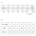
- FIG. 3 shows a design example of the reflector 10 of the first embodiment.
- FIG. 3A shows the arrangement of conductor patterns 131a to 131g forming the conductive layer 13.
- FIG. 3B shows the size and phase of each conductor pattern.
- the conductor patterns 131a to 131g are cross patterns with equal vertical and horizontal lengths.
- the size of each conductor pattern 131 is indicated by vertical or horizontal lengths L1 to L7.
- the pitch of the conductor patterns 131a to 131g that is, the center-to-center distance d is set to 1/2 of the working wavelength. Since the wavelength ⁇ of the 28 GHz band is 10.8 mm, the pitch of the conductor patterns 131a-131g is 5.4 mm.
- a reflection angle of 35° is aimed at by arranging the conductor patterns 131a to 131g.
- the angle of reflection in this case is the angle of reflection when radio waves are incident perpendicularly to the reflector 10, that is, the angle of reflection with respect to the normal line.
- the phase difference is 103°.
- the sizes of the conductor patterns 131a to 131g, that is, the lengths of L1 to L7 are determined so as to obtain this phase difference.
- the shape of the conductor pattern 131 is not limited to a cross pattern, and circular, elliptical, polygonal, etc. of different sizes may be provided at a predetermined cycle.
- the size of the conductor pattern 131 is 2 to 5 mm when the 28 GHz band is targeted, but the size of the conductor pattern 131 is appropriately designed according to the frequency band.
- a radio wave with a frequency determined by the size and period of the conductor pattern 131 is selectively reflected.
- the frequency band selected by resonance is narrow, but by setting the dielectric constant of the dielectric layer 11 to 2.0 or less, the frequency band selected as described later is expanded to a bandwidth of 4 GHz or more, more preferably 6 GHz or more.
- the selected frequency bandwidth can vary with the thickness of the dielectric layer 11 of the reflector 10, thus achieving a broadband reflector with a bandwidth per unit thickness (1 mm) of the reflector 10 exceeding 6.5 GHz/mm.
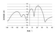
- FIG. 4 shows the reflection characteristics of the reflector 10 with the design of FIG.
- the horizontal axis is the angle
- the vertical axis is the reflection intensity (dB).
- a main peak is observed in the direction of 35°, confirming that the reflector 10 can control the direction of reflection of radio waves almost as designed.
- the bandwidth of the 35° main lobe that is, the frequency range where the peak falls by 3 dB is 4 GHz or more, more preferably 6 GHz or more.
- Oblique reflection characteristics covering a wide frequency band of the reflector 10 are exhibited in a frequency band of 24 GHz to 60 GHz.
- the frequency band of reflection refers to a frequency range in which the peak intensity of the main lobe of the reflected wave toward the target with respect to the incident wave of the working wavelength is attenuated by 3 dB.
- FIG. 5 shows the reflection characteristics of a low-permittivity reflector for incident waves of different frequencies.
- the low dielectric constant reflector is the reflector of the embodiment, and is reflector 10 using dielectric layer 11 having a relative dielectric constant of 2.0 or less.
- a dielectric layer with a dielectric constant ⁇ of 1.88 is used.
- FIG. 6 shows reflection characteristics of a high dielectric constant reflector for incident waves of different frequencies.
- a high-permittivity reflector is a reflector that uses a dielectric layer with a relative permittivity greater than 2.0.
- reflection spectra at 26 GHz, 28 GHz, and 31 GHz are calculated using the dielectric layer 11 with a dielectric constant ⁇ of 1.88.
- Reflection intensity on the vertical axis is indicated by a scattering cross section (RCS: Radar Cross Section), which is an index representing reflectivity.
- RCS Radar Cross Section
- a plane wave in each frequency band of 26 GHz, 28 GHz, and 31 GHz is incident from the normal direction of the reflector, and the scattering cross section is analyzed for each angle with Dassault Systèmes CST Studio Suite, a general-purpose three-dimensional electromagnetic field simulation software.
- the reflection spectrum peak appears in the direction of 35° at any of 26 GHz, 28 GHz, and 31 GHz.
- the peak value is within the range of ⁇ 25 dB ⁇ 2.5 dB, and a stable peak intensity is obtained at a target reflection angle of 35° over at least a 5 GHz band.
- the main lobe with a reflection angle of 35° is clearly distinguished from the other side lobes, and the incident wave is reflected in the target direction of 35° with good controllability.
- another peak appears at 0° and -65°.
- the 0° peak corresponds to loss since it is reflected in the same direction as the incident.
- the -65° peak is a reflection in the opposite direction of the target at 35°, and depending on the environment in which the reflector is used, it may be a loss or it may be an advantage to deliver radio waves in two directions at once.
- the dielectric constant ⁇ is changed to 3.62, and other conditions such as the conductor pattern are kept the same as those of the reflector of FIG.
- Materials with a dielectric constant of 3.62 include polyphenylene ether (PPE) and acrylic resin.
- PPE polyphenylene ether
- acrylic resin acrylic resin.
- FIG. 6 represents the fact that the metasurface using resonance deteriorates the reflection characteristics as the frequency changes.
- the reflection frequency band can be expanded by lowering the dielectric constant of the dielectric layer 11 used in the reflector 10 to some extent.
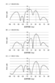
- FIG. 7A shows the reflection range of the low dielectric constant reflector
- FIG. 7B shows the reflection range of the high dielectric constant reflector.
- 7A and 7B the horizontal axis is the reflection direction and the vertical axis is the frequency.
- the model of the reflector used has the same conductor pattern as in FIG. 3A formed on the surface of the dielectric layer.
- the relative dielectric constant ⁇ of the low dielectric constant reflector in FIG. 7A is set to 1.88
- the relative dielectric constant ⁇ of the high dielectric constant reflector in FIG. 7B is set to 3.62.
- a high reflection intensity (more than -30 dB and less than -20 dB) is obtained from 24 GHz to 33 GHz in the 35° direction of the target.
- the reflection intensity is distributed in the range of ⁇ 10° centering on 35°, and in particular, in the range of 23° or more and 35° or less, the reflection intensity exceeds -30 dB and -20 dB or less over the frequency band of 10 GHz or more.
- a wide range of reflected frequency characteristics provides high resistance to environmental changes.
- FIG. 7B when the dielectric constant is 3.62, a high reflection intensity (more than -30 dB and less than -20 dB) is obtained from 21 GHz to 28.5 GHz in the direction of 35° of the target.
- the practical frequency band of the reflector in FIG. 7B is in the range of 24 GHz to 28.5 GHz.
- a reflector having a frequency band of 6 GHz or more in the frequency band of 24 GHz or more and 60 GHz or less is desirable.
- FIG. 8 shows the relationship between thickness and bandwidth for dielectric layers with different dielectric constants.
- FIG. 9 shows the relationship between the thickness of dielectric layers with different dielectric constants and the reflection intensity.
- the thickness of the dielectric layer 11 is changed to 0.30 mm, 0.50 mm and 0.75 mm.
- the conductor pattern 131 formed on the first surface 111 of the dielectric layer 11 is the same as in FIG. 3A.
- the pattern configuration of the conductors is the same, but the dielectric constant ⁇ of the dielectric layer 11 is made different.
- a plane wave of 28 GHz is incident from the normal direction of the reflector and the bandwidth of the reflected wave is analyzed.
- the bandwidth of the reflected wave is the frequency bandwidth attenuated 3 dB from the peak value of the main lobe of the reflection, as described above.
- the thickness of the dielectric layer 11 When the thickness of the dielectric layer 11 is the same, the lower the dielectric constant ⁇ , the wider the reflection bandwidth. Conversely, a material with a low dielectric constant allows the reflector to be made thinner while achieving the same bandwidth.
- a bandwidth of over 6.5 GHz is achieved with a reflector with ⁇ of 1.88, whereas a reflector with ⁇ of 3.62 can only cover a bandwidth of 4.5 GHz.
- the reflection frequency bandwidth exceeds 6 GHz in the frequency band from 24 GHz to 30 GHz.
- a bandwidth of 6 GHz might be achievable by increasing the thickness of the dielectric layer 11 with ⁇ of 3.62 to around 1.2 m.
- the reflector becomes thicker and less flexible, limiting its range of application.
- ⁇ is 1.88
- a bandwidth of 6.5 GHz is realized with a thickness of the dielectric layer 11 of 0.75 mm, and a sheet-like flexible reflector is realized.
- a sheet-like reflector is easy to handle and can be applied to a desired location like wallpaper. It is a great advantage that a thin and flexible dielectric layer 11 can achieve a wide band.
- the peak intensity of the reflected wave is calculated by changing the thickness of the dielectric layer 11 to 0.25 mm, 0.30 mm, 0.50 mm, and 0.80 mm.
- the dielectric constant ⁇ is 1.88
- a peak intensity exceeding ⁇ 24 dB can be obtained by setting the thickness of the dielectric layer 11 to 0.30 mm or more.
- ⁇ is 3.62
- the same level of peak intensity cannot be obtained unless the thickness of the dielectric layer 11 is 0.5 mm.
- the low dielectric constant reflector of the embodiment is also advantageous from the viewpoint of thinning and weight reduction of the device.
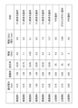
- FIG. 10 shows the configurations and characteristics of an example and a comparative example.
- Structural parameters are the type, thickness, dielectric constant, and porosity of the base material that constitutes the dielectric layer 11 . Vary the values of these parameters.
- the frequency band of the reflected wave and the bandwidth per unit thickness are shown.
- the conductor pattern 131 is the conductor patterns 131a-131g of FIG.
- Incident wave wavelength 10.7 mm (frequency 28 GHz)
- Incident wave frequency change range 20 GHz to 35 GHz
- Incident angle of incident wave with respect to the normal direction of the reflector 0 degrees
- First desired reflection angle ⁇ of the reflection spectrum with respect to the normal direction of the reflector 35 degrees
- Example 1 a fluorine porous substrate is used as the base material of the dielectric layer 11 .
- a fluorine porous substrate is a combination of a fluororesin and an inorganic porous aggregate.
- Polytetrafluoroethylene is used as the fluorinated resin.
- This dielectric substrate has a thickness of 0.75 mm, a porosity of 33.2%, and a dielectric constant of 1.88.
- the frequency band of reflection obtained in Example 1 is 6.6 GHz, and the band per unit thickness (1 mm) is 8.8 GHz/mm.
- Example 2 a fluorine porous substrate is used as the base material of the dielectric layer 11 .
- This dielectric substrate has a thickness of 0.75 mm, a porosity of 67.7%, and a dielectric constant of 1.50.
- the dielectric layer 11 is designed to have a different porosity and relative permittivity by changing the aggregation density of the porous inorganic fine particles used in the fluorine porous substrate.
- the frequency band of reflection obtained in Example 2 is 7.1 GHz, and the band per unit thickness (1 mm) is 9.5 GHz/mm.
- Example 3 a fluorine porous substrate is used as the base material of the dielectric layer 11 .
- This dielectric substrate has a thickness of 0.50 mm, a porosity of 33.0%, and a dielectric constant of 1.88.
- the dielectric layer 11 is designed to have a different porosity and relative permittivity by changing the aggregation density of the porous inorganic fine particles used in the fluorine porous substrate. Also, the dielectric layer 11 is made thinner than in the first and second embodiments.
- the frequency band of reflection obtained in Example 3 is 4.55 GHz, and the band per unit thickness (1 mm) is 9.1 GHz/mm.
- Example 4 a fluorine porous substrate is used as the base material of the dielectric layer 11 .
- This dielectric substrate has a thickness of 1.00 mm, a porosity of 33.0%, and a dielectric constant of 1.88.
- the thickness of the dielectric layer 11 is made thicker than in the first and second embodiments.
- the frequency band of reflection obtained in Example 4 is 6.5 GHz, and the band per unit thickness (1 mm) is 6.5 GHz/mm.
- Example 5 a fluorine porous substrate is used as the base material of the dielectric layer 11 .
- This dielectric substrate has a thickness of 0.75 mm, a porosity of 22.5%, and a dielectric constant of 2.00.
- the frequency band of reflection obtained in Example 5 is 5.5 GHz, and the band per unit thickness (1 mm) is 7.3 GHz/mm.
- Example 6 a fluorine porous substrate is used as the base material of the dielectric layer 11 .
- This dielectric substrate has a thickness of 0.3 mm, a porosity of 33.0%, and a dielectric constant of 1.88.
- the thickness of the dielectric layer 11 is made thinner than that of the fifth embodiment.
- the frequency band of reflection obtained in Example 6 is 4.1 GHz, and the band per unit thickness (1 mm) is 13.7 GHz.
- Comparative Example 1 PPE is used as the base material of the dielectric layer 11 .
- the PPE substrate has a thickness of 0.75 mm, a porosity of 0.0%, and a dielectric constant of 3.62.
- the frequency band of reflection obtained in Comparative Example 1 is 4.5 GHz, and the band per unit thickness (1 mm) is 6.0 GHz/mm.
- the frequency band of reflection is narrower due to the higher dielectric constant.
- Comparative Example 2 a glass epoxy base material is used as the base material of the dielectric layer 11 .
- This dielectric substrate has a thickness of 0.75 mm, a porosity of 0.0%, and a dielectric constant of 5.00.
- the dielectric constant is higher than that of Comparative Example 1.
- the frequency band of reflection obtained in Comparative Example 2 is 3.7 GHz, and the band per unit thickness (1 mm) is 4.9 GHz/mm.
- Comparative Example 3 PPE is used as the base material of the dielectric layer 11 .
- This dielectric substrate has a thickness of 0.50 mm, a porosity of 0.0%, and a dielectric constant of 3.62.
- the frequency band of reflection obtained in Comparative Example 3 is 3.0 GHz, and the band per unit thickness (1 mm) is 6.0 GHz.
- the same PPE base material as in Comparative Example 1 is used, the reduced thickness of the base material further narrows the reflection frequency band.
- broadband reflection characteristics exceeding 6.5 GHz per unit thickness, preferably exceeding 7.0 GHz, and more preferably exceeding 8.0 GHz are obtained when the dielectric constant of the dielectric layer 11 is 2.0 or less.
- the dielectric layer is thin and has a dielectric constant of 1.88 or less, a frequency band of 8.8 GHz or more is realized per unit thickness.
- a dielectric constant of 2.0 or less can be realized with a porosity of about 20% for the dielectric layer 11 .
- the thickness of the dielectric layer 11 can be appropriately designed according to the application.
- dielectric layer 11 may have a thickness of 0.3 mm or more and 1.0 mm or less. By setting the thickness of the dielectric layer 11 to 0.3 mm or more, the reflector 10 with high robustness can be obtained. Further, if the thickness of the dielectric layer 11 is 1.0 mm or less, it is advantageous for weight reduction in the design of a large reflector having a side of about 1 m, and is excellent in workability and construction cost. In addition, when the thickness is 0.3 mm, 1.0 mm, etc., it includes an allowable manufacturing error.
- FIG. 11 is a schematic diagram of the reflector 20 of the second embodiment.
- the main part of the reflector 20 is the same as that of the reflector 10 of the first embodiment, and a dielectric layer 21 having a dielectric constant of 2.0 or less is used.
- a conductive layer 23 including a predetermined conductive pattern 231 is formed on the first surface 211 of the dielectric layer 21 , and the ground layer 22 is provided on the second surface 212 .
- the conductor pattern 231 is designed such that the reflection direction of the main lobe with respect to the incident wave of the 28 GHz band is inclined by a predetermined angle from the normal direction. An example of the pattern is shown in FIG. 3A.
- a protective layer 24 is provided to cover the conductive layer 23 .
- An adhesive layer 26 is provided on the ground layer 22 side.
- the adhesive layer 26 allows the reflector 20 to be attached to a desired position such as a wall surface or a ceiling.
- the protective layer 24 is transparent to incident waves between 24 GHz and 30 GHz. Transparent to an incident wave means having a transmittance of 60% or more, preferably 70% or more, more preferably 80% or more, and even more preferably 90% or more to an incident wave.
- Protective layer 24 may be transparent to visible light.
- the protective layer 24 protects the conductor pattern 231 of the reflector 20 from deterioration and damage due to external factors, and obtains excellent durability.
- the conductor pattern 231 of the reflector 20 is subject to oxidative deterioration over time, such as contact with oxygen and moisture in the atmosphere.
- the protective layer 24 preferably has a thickness of 0.1 mm or more and 1.0 mm or less and a dielectric constant of 2.0 or less.
- simulation was performed under the following conditions, and the reflection angle deviation (%) and the reflection intensity loss (%) of the examples and comparative examples were obtained from the far radiation field, intensity, and angle of the reflection spectrum for the incident wave.
- ⁇ Wavelength of incident wave 10.7 mm (frequency 28 GHz) ⁇ Frequency change range of incident wave: 20GHz-35GHz Incident angle of incident wave with respect to the normal direction of the reflector: 0 degree First desired reflection angle ⁇ of the reflection spectrum with respect to the normal direction of the reflector: -43 degrees
- Five cross patterns of different sizes are used as the shape of the conductor pattern, and the reflection angle and reflection intensity are calculated by changing the thickness and dielectric constant of the protective layer 24 covering the conductor pattern.
- FIG. 12 shows the results of the simulation.
- “Ref” in the leftmost column of FIG. 12 indicates a reference configuration in which the protective layer 24 is not provided.
- the protective layer 24 has a thickness of 0.0 mm and a dielectric constant of 1.0.
- the unit of reflection intensity for the reference configuration is (dB).
- “Reflection angle deviation” indicates the rate of change (%) from the reflection angle of the reference configuration
- “Reflection intensity loss” indicates the rate (%) of decrease from the reflection intensity of the reference configuration.
- Reflection angle shift and reflection intensity loss were evaluated as follows. ⁇ Reflection angle deviation is 10% or less: A ⁇ Reflection angle deviation exceeds 10%: B ⁇ Reflection intensity loss is 5% or less: S ⁇ Reflection intensity loss is 10% or less: A ⁇ Reflection intensity loss exceeds 10%: B ⁇ Comprehensive evaluation Pass: Evaluation of both reflection angle deviation and reflection intensity loss is "A" Failed: Either the reflection angle deviation or reflection intensity loss evaluation is "B"
- Examples 7 to 10 passed. Moreover, in Examples 7 to 9, the reflection intensity loss was small, and more favorable results were obtained.
- the relative dielectric constant Dk is high, the reflection angle shift and reflection intensity loss are large, and the relative dielectric constant Dk is preferably 2.0 or less.
- the dielectric constant is 1.5 or less, the reflection intensity loss is 5% or less, which is more preferable (“S” evaluation in FIG. 12). If the thickness of the protective layer 24 is large, the deviation of the reflection angle and the loss of the reflection intensity are large.
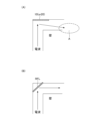
- FIG. 13 shows a usage example of the reflector 20 of the embodiment in comparison with usage of a normal reflector.
- (A) of FIG. 13 shows a mode of use of the reflector 10 or 20 of the embodiment.
- the thin and flexible embodiment reflectors 10 or 20 can be installed along L-shaped corridors, streets, corridors, and the like.
- the reflector of the embodiment has a metasurface including a periodic array of a plurality of conductor patterns 131, and reflects incident waves in directions other than specular reflection. As shown in FIG. 12, when radio waves are vertically incident on the reflector 10 or 20 installed on the wall surface of the corner, the incident radio waves are reflected at oblique angles other than the vertical and horizontal directions of the reflector. As a result, radio waves can be sent to smartphones, electronic devices, lighting devices, and the like located in area A.
- a normal reflector RFL with a specular reflection surface reflects vertically incident radio waves in the direction of incidence. Therefore, the reflector RFL must be installed at an oblique angle with respect to the incident radio wave. When placed in a corner as shown in FIG. 13B, the space cannot be effectively utilized. On the other hand, the reflector 10 or 20 of the embodiment can reduce the dead zone of radio waves without taking up space and spoiling the appearance.
- the reflector of the embodiment can extend the frequency band of reflection and improve resistance to the environment by using a dielectric layer with a low dielectric constant.
- the thickness of the reflector can be reduced, and the range of application can be expanded.
- the surface of the adhesive layer 26 may be protected with a protective film, and the protective film may be peeled off at the time of use and applied to a desired location.
- the reflectors of the embodiments may be used in combination with small cells or repeaters. In this case, the dead zone can be further reduced without increasing the number of devices such as small cells and repeaters and without taking up space for installing reflectors.
- (Section 1) a dielectric layer; a conductive layer provided on the first surface of the dielectric layer and comprising a periodic array of a plurality of conductive patterns; a ground layer provided on a second surface opposite to the first surface; has the conductive layer reflects an incident wave at an angle different in magnitude from the angle of incidence;
- the dielectric layer has a dielectric constant of 2.0 or less.
- reflector. the conductive layer forms a reflective surface of the reflector; Item 2.
- the reflector according to Item 1 wherein an adhesive layer is provided on the side opposite to the reflecting surface.
- the reflector according to Item 1 or 2 having: (Section 4) a protective layer covering the conductive layer; 4.
- the protective layer has a thickness of 0.1 mm or more and 1.0 mm or less and a dielectric constant of 2.0 or less.
- the reflector according to Item 4 (Item 6)
- the dielectric layer has a thickness of 0.3 mm or more and 1.0 m or less.
- Item 6. A reflector according to any one of Items 1 to 5.
- (Section 7) The size of the conductor pattern is 2 mm or more and 5 mm or less.
- Item 7. A reflector according to any one of Items 1 to 6.
- the bandwidth of reflected frequencies per unit thickness of the reflector is greater than 6.5 GHz/mm;
- Item 8 A reflector according to any one of Items 1 to 7.
- the dielectric layer is formed of a combination of a fluorinated resin and an inorganic porous aggregate, and the porosity of the dielectric layer is 20% or more.
- Item 9 A reflector according to any one of Items 1 to 8.
Landscapes
- Physics & Mathematics (AREA)
- Electromagnetism (AREA)
- General Physics & Mathematics (AREA)
- Optics & Photonics (AREA)
- Aerials With Secondary Devices (AREA)
Priority Applications (5)
| Application Number | Priority Date | Filing Date | Title |
|---|---|---|---|
| CN202380022310.0A CN118715673A (zh) | 2022-01-19 | 2023-01-13 | 反射器 |
| JP2023575231A JP7745656B2 (ja) | 2022-01-19 | 2023-01-13 | リフレクタ |
| US18/730,130 US20250110265A1 (en) | 2022-01-19 | 2023-01-13 | Reflector |
| KR1020247027031A KR20240136381A (ko) | 2022-01-19 | 2023-01-13 | 리플렉터 |
| EP23743187.9A EP4468521A4 (en) | 2022-01-19 | 2023-01-13 | REFLECTOR |
Applications Claiming Priority (2)
| Application Number | Priority Date | Filing Date | Title |
|---|---|---|---|
| JP2022006361 | 2022-01-19 | ||
| JP2022-006361 | 2022-01-19 |
Publications (1)
| Publication Number | Publication Date |
|---|---|
| WO2023140193A1 true WO2023140193A1 (ja) | 2023-07-27 |
Family
ID=87348758
Family Applications (1)
| Application Number | Title | Priority Date | Filing Date |
|---|---|---|---|
| PCT/JP2023/000797 Ceased WO2023140193A1 (ja) | 2022-01-19 | 2023-01-13 | リフレクタ |
Country Status (7)
| Country | Link |
|---|---|
| US (1) | US20250110265A1 (https=) |
| EP (1) | EP4468521A4 (https=) |
| JP (1) | JP7745656B2 (https=) |
| KR (1) | KR20240136381A (https=) |
| CN (1) | CN118715673A (https=) |
| TW (1) | TW202345464A (https=) |
| WO (1) | WO2023140193A1 (https=) |
Cited By (3)
| Publication number | Priority date | Publication date | Assignee | Title |
|---|---|---|---|---|
| JP7501749B1 (ja) | 2023-08-01 | 2024-06-18 | Toppanホールディングス株式会社 | 機能層付きリフレクトアレイ |
| WO2025027966A1 (ja) * | 2023-08-01 | 2025-02-06 | Toppanホールディングス株式会社 | 電磁波反射板および電磁波反射装置 |
| WO2025094949A1 (ja) * | 2023-10-31 | 2025-05-08 | 積水化学工業株式会社 | ノイズ除去体 |
Citations (8)
| Publication number | Priority date | Publication date | Assignee | Title |
|---|---|---|---|---|
| US4897151A (en) * | 1988-07-27 | 1990-01-30 | General Dynamics Corp., Pomona Division | Method for fabricating a dichroic parabolic lens reflector |
| US6067050A (en) * | 1997-05-22 | 2000-05-23 | Her Majesty The Queen In Right Of Canada, As Represented By The Minister Of Industry Through The Communications Research Centre | Techniques for the cancellation of beam squint in planar printed reflectors |
| JP2012060530A (ja) * | 2010-09-10 | 2012-03-22 | Yagi Antenna Co Ltd | 平面状反射板 |
| JP5177708B2 (ja) | 2010-08-27 | 2013-04-10 | 株式会社エヌ・ティ・ティ・ドコモ | リフレクトアレイ |
| WO2014020969A1 (ja) * | 2012-07-31 | 2014-02-06 | 株式会社 エヌ・ティ・ティ・ドコモ | リフレクトアレー |
| JP2017171898A (ja) | 2016-03-18 | 2017-09-28 | 日東電工株式会社 | 絶縁樹脂材料、それを用いた金属層付絶縁樹脂材料および配線基板 |
| JP2021175054A (ja) * | 2020-04-22 | 2021-11-01 | Kddi株式会社 | メタサーフェス反射板アレイ |
| JP2022006361A (ja) | 2020-06-24 | 2022-01-13 | 医療法人すぎやま内科 | 経皮吸収用組成物 |
Family Cites Families (5)
| Publication number | Priority date | Publication date | Assignee | Title |
|---|---|---|---|---|
| JPS5419605Y2 (https=) | 1974-12-13 | 1979-07-19 | ||
| ES2153323B1 (es) * | 1999-06-07 | 2001-07-16 | Univ Madrid Politecnica | Reflectores planos en tecnologia impresa multicapa y su procedimiento de diseño. |
| JP5371633B2 (ja) | 2008-09-30 | 2013-12-18 | 株式会社エヌ・ティ・ティ・ドコモ | リフレクトアレイ |
| JP6037761B2 (ja) | 2012-10-18 | 2016-12-07 | 三菱電機株式会社 | アンテナ装置 |
| JP7500172B2 (ja) * | 2019-09-18 | 2024-06-17 | 電気興業株式会社 | メタサーフェス反射板および該メタサーフェスを備えた信号機 |
-
2023
- 2023-01-13 US US18/730,130 patent/US20250110265A1/en active Pending
- 2023-01-13 JP JP2023575231A patent/JP7745656B2/ja active Active
- 2023-01-13 KR KR1020247027031A patent/KR20240136381A/ko active Pending
- 2023-01-13 CN CN202380022310.0A patent/CN118715673A/zh active Pending
- 2023-01-13 WO PCT/JP2023/000797 patent/WO2023140193A1/ja not_active Ceased
- 2023-01-13 EP EP23743187.9A patent/EP4468521A4/en active Pending
- 2023-01-17 TW TW112101989A patent/TW202345464A/zh unknown
Patent Citations (8)
| Publication number | Priority date | Publication date | Assignee | Title |
|---|---|---|---|---|
| US4897151A (en) * | 1988-07-27 | 1990-01-30 | General Dynamics Corp., Pomona Division | Method for fabricating a dichroic parabolic lens reflector |
| US6067050A (en) * | 1997-05-22 | 2000-05-23 | Her Majesty The Queen In Right Of Canada, As Represented By The Minister Of Industry Through The Communications Research Centre | Techniques for the cancellation of beam squint in planar printed reflectors |
| JP5177708B2 (ja) | 2010-08-27 | 2013-04-10 | 株式会社エヌ・ティ・ティ・ドコモ | リフレクトアレイ |
| JP2012060530A (ja) * | 2010-09-10 | 2012-03-22 | Yagi Antenna Co Ltd | 平面状反射板 |
| WO2014020969A1 (ja) * | 2012-07-31 | 2014-02-06 | 株式会社 エヌ・ティ・ティ・ドコモ | リフレクトアレー |
| JP2017171898A (ja) | 2016-03-18 | 2017-09-28 | 日東電工株式会社 | 絶縁樹脂材料、それを用いた金属層付絶縁樹脂材料および配線基板 |
| JP2021175054A (ja) * | 2020-04-22 | 2021-11-01 | Kddi株式会社 | メタサーフェス反射板アレイ |
| JP2022006361A (ja) | 2020-06-24 | 2022-01-13 | 医療法人すぎやま内科 | 経皮吸収用組成物 |
Non-Patent Citations (1)
| Title |
|---|
| See also references of EP4468521A4 |
Cited By (4)
| Publication number | Priority date | Publication date | Assignee | Title |
|---|---|---|---|---|
| JP7501749B1 (ja) | 2023-08-01 | 2024-06-18 | Toppanホールディングス株式会社 | 機能層付きリフレクトアレイ |
| WO2025027966A1 (ja) * | 2023-08-01 | 2025-02-06 | Toppanホールディングス株式会社 | 電磁波反射板および電磁波反射装置 |
| JP7639978B2 (ja) | 2023-08-01 | 2025-03-05 | Toppanホールディングス株式会社 | 機能層付きリフレクトアレイ |
| WO2025094949A1 (ja) * | 2023-10-31 | 2025-05-08 | 積水化学工業株式会社 | ノイズ除去体 |
Also Published As
| Publication number | Publication date |
|---|---|
| TW202345464A (zh) | 2023-11-16 |
| EP4468521A1 (en) | 2024-11-27 |
| CN118715673A (zh) | 2024-09-27 |
| US20250110265A1 (en) | 2025-04-03 |
| KR20240136381A (ko) | 2024-09-13 |
| JP7745656B2 (ja) | 2025-09-29 |
| EP4468521A4 (en) | 2026-01-07 |
| JPWO2023140193A1 (https=) | 2023-07-27 |
Similar Documents
| Publication | Publication Date | Title |
|---|---|---|
| JP7745656B2 (ja) | リフレクタ | |
| Kakhki et al. | Millimeter-wave beam-tilting Vivaldi antenna with gain enhancement using multilayer FSS | |
| KR100976858B1 (ko) | 저 레이더 반사면적의 평면 패치 안테나와 평면 패치어레이 안테나 | |
| KR101756816B1 (ko) | 소형화된 단위구조의 반복 배열을 가지는 대역 저지 동작 주파수 선택 표면구조 | |
| Kossifos et al. | A NRI-TL metamaterial leaky-wave antenna radiating at broadside with zero beam-squinting | |
| JPWO2023140193A5 (https=) | ||
| Panda et al. | Wideband and high gain tuning fork shaped monopole antenna using high impedance surface | |
| Ren et al. | Wideband RCS reduction for circular-polarized slot array antennas based on composite metasurface | |
| Danesh et al. | Wide-incidence angle and polarisation insensitive transparent metasurface for 5g outdoor to indoor coverage enhancement | |
| WO2024204610A9 (ja) | リフレクタ | |
| KR20250153234A (ko) | 리플렉터 | |
| Yan et al. | A single layer ultra-miniaturized FSS operating in VHF | |
| Patel et al. | Wideband RCS reduction of microstrip antenna using artificial magnetic conductor metasurface | |
| Oraizi et al. | Design of metamaterial multilayer structures as frequency selective surfaces | |
| Nguyen et al. | Dual band and dual polarized reflectarray using cross dipole and patch elements | |
| TW202501888A (zh) | 反射器、輥體、輥體之製造方法 | |
| CN121216133B (zh) | 一种面向微波辐射计干扰的双极化多功能有源反射透射器 | |
| Yao et al. | High efficiency and high gain indium tin oxide optical transparent antenna based on Fabry–Perot cavity | |
| Hou et al. | A dielectric-loaded FSS-based radome design with an adjustable RCS reduction band | |
| Roehrner et al. | A broadband inhomogeneous frequency selective surface on quartz glass substrate | |
| Abhijay et al. | A Circularly Polarized MIMO Antenna with FSS-Based Decoupling for V2X Applications | |
| CN119093002A (zh) | 双层结构透明天线 | |
| Chen et al. | Broadband reflectarray antenna using a novel multifrequency phase synthesis method | |
| Murakami et al. | Scattering Characteristics of Metamaterial-based Electromagnetic Scattering Sheet with a Protective Layer | |
| CN120222001A (zh) | 一种低损耗可移植的天线罩结构 |
Legal Events
| Date | Code | Title | Description |
|---|---|---|---|
| 121 | Ep: the epo has been informed by wipo that ep was designated in this application |
Ref document number: 23743187 Country of ref document: EP Kind code of ref document: A1 |
|
| ENP | Entry into the national phase |
Ref document number: 2023575231 Country of ref document: JP Kind code of ref document: A |
|
| WWE | Wipo information: entry into national phase |
Ref document number: 18730130 Country of ref document: US |
|
| ENP | Entry into the national phase |
Ref document number: 20247027031 Country of ref document: KR Kind code of ref document: A |
|
| WWE | Wipo information: entry into national phase |
Ref document number: 202380022310.0 Country of ref document: CN |
|
| WWE | Wipo information: entry into national phase |
Ref document number: 2023743187 Country of ref document: EP |
|
| NENP | Non-entry into the national phase |
Ref country code: DE |
|
| ENP | Entry into the national phase |
Ref document number: 2023743187 Country of ref document: EP Effective date: 20240819 |
|
| WWP | Wipo information: published in national office |
Ref document number: 18730130 Country of ref document: US |