WO2023140166A1 - 超音波プローブおよび超音波プローブの製造方法 - Google Patents
超音波プローブおよび超音波プローブの製造方法 Download PDFInfo
- Publication number
- WO2023140166A1 WO2023140166A1 PCT/JP2023/000563 JP2023000563W WO2023140166A1 WO 2023140166 A1 WO2023140166 A1 WO 2023140166A1 JP 2023000563 W JP2023000563 W JP 2023000563W WO 2023140166 A1 WO2023140166 A1 WO 2023140166A1
- Authority
- WO
- WIPO (PCT)
- Prior art keywords
- ultrasonic probe
- piezoelectric body
- piezoelectric
- electrode
- piezoelectric element
- Prior art date
- Legal status (The legal status is an assumption and is not a legal conclusion. Google has not performed a legal analysis and makes no representation as to the accuracy of the status listed.)
- Ceased
Links
Images


Classifications
-
- H—ELECTRICITY
- H10—SEMICONDUCTOR DEVICES; ELECTRIC SOLID-STATE DEVICES NOT OTHERWISE PROVIDED FOR
- H10N—ELECTRIC SOLID-STATE DEVICES NOT OTHERWISE PROVIDED FOR
- H10N30/00—Piezoelectric or electrostrictive devices
- H10N30/80—Constructional details
- H10N30/87—Electrodes or interconnections, e.g. leads or terminals
- H10N30/877—Conductive materials
- H10N30/878—Conductive materials the principal material being non-metallic, e.g. oxide or carbon based
-
- A—HUMAN NECESSITIES
- A61—MEDICAL OR VETERINARY SCIENCE; HYGIENE
- A61B—DIAGNOSIS; SURGERY; IDENTIFICATION
- A61B8/00—Diagnosis using ultrasonic, sonic or infrasonic waves
- A61B8/42—Details of probe positioning or probe attachment to the patient
- A61B8/4272—Details of probe positioning or probe attachment to the patient involving the acoustic interface between the transducer and the tissue
- A61B8/4281—Details of probe positioning or probe attachment to the patient involving the acoustic interface between the transducer and the tissue characterised by sound-transmitting media or devices for coupling the transducer to the tissue
-
- A—HUMAN NECESSITIES
- A61—MEDICAL OR VETERINARY SCIENCE; HYGIENE
- A61B—DIAGNOSIS; SURGERY; IDENTIFICATION
- A61B8/00—Diagnosis using ultrasonic, sonic or infrasonic waves
- A61B8/44—Constructional features of the ultrasonic, sonic or infrasonic diagnostic device
- A61B8/4483—Constructional features of the ultrasonic, sonic or infrasonic diagnostic device characterised by features of the ultrasound transducer
-
- B—PERFORMING OPERATIONS; TRANSPORTING
- B06—GENERATING OR TRANSMITTING MECHANICAL VIBRATIONS IN GENERAL
- B06B—METHODS OR APPARATUS FOR GENERATING OR TRANSMITTING MECHANICAL VIBRATIONS OF INFRASONIC, SONIC, OR ULTRASONIC FREQUENCY, e.g. FOR PERFORMING MECHANICAL WORK IN GENERAL
- B06B1/00—Methods or apparatus for generating mechanical vibrations of infrasonic, sonic, or ultrasonic frequency
- B06B1/02—Methods or apparatus for generating mechanical vibrations of infrasonic, sonic, or ultrasonic frequency making use of electrical energy
- B06B1/06—Methods or apparatus for generating mechanical vibrations of infrasonic, sonic, or ultrasonic frequency making use of electrical energy operating with piezoelectric effect or with electrostriction
- B06B1/0607—Methods or apparatus for generating mechanical vibrations of infrasonic, sonic, or ultrasonic frequency making use of electrical energy operating with piezoelectric effect or with electrostriction using multiple elements
- B06B1/0622—Methods or apparatus for generating mechanical vibrations of infrasonic, sonic, or ultrasonic frequency making use of electrical energy operating with piezoelectric effect or with electrostriction using multiple elements on one surface
-
- B—PERFORMING OPERATIONS; TRANSPORTING
- B06—GENERATING OR TRANSMITTING MECHANICAL VIBRATIONS IN GENERAL
- B06B—METHODS OR APPARATUS FOR GENERATING OR TRANSMITTING MECHANICAL VIBRATIONS OF INFRASONIC, SONIC, OR ULTRASONIC FREQUENCY, e.g. FOR PERFORMING MECHANICAL WORK IN GENERAL
- B06B1/00—Methods or apparatus for generating mechanical vibrations of infrasonic, sonic, or ultrasonic frequency
- B06B1/02—Methods or apparatus for generating mechanical vibrations of infrasonic, sonic, or ultrasonic frequency making use of electrical energy
- B06B1/06—Methods or apparatus for generating mechanical vibrations of infrasonic, sonic, or ultrasonic frequency making use of electrical energy operating with piezoelectric effect or with electrostriction
- B06B1/0644—Methods or apparatus for generating mechanical vibrations of infrasonic, sonic, or ultrasonic frequency making use of electrical energy operating with piezoelectric effect or with electrostriction using a single piezoelectric element
- B06B1/0662—Methods or apparatus for generating mechanical vibrations of infrasonic, sonic, or ultrasonic frequency making use of electrical energy operating with piezoelectric effect or with electrostriction using a single piezoelectric element with an electrode on the sensitive surface
-
- G—PHYSICS
- G01—MEASURING; TESTING
- G01N—INVESTIGATING OR ANALYSING MATERIALS BY DETERMINING THEIR CHEMICAL OR PHYSICAL PROPERTIES
- G01N29/00—Investigating or analysing materials by the use of ultrasonic, sonic or infrasonic waves; Visualisation of the interior of objects by transmitting ultrasonic or sonic waves through the object
- G01N29/04—Analysing solids
-
- G—PHYSICS
- G01—MEASURING; TESTING
- G01N—INVESTIGATING OR ANALYSING MATERIALS BY DETERMINING THEIR CHEMICAL OR PHYSICAL PROPERTIES
- G01N29/00—Investigating or analysing materials by the use of ultrasonic, sonic or infrasonic waves; Visualisation of the interior of objects by transmitting ultrasonic or sonic waves through the object
- G01N29/22—Details, e.g. general constructional or apparatus details
- G01N29/228—Details, e.g. general constructional or apparatus details related to high temperature conditions
-
- G—PHYSICS
- G01—MEASURING; TESTING
- G01N—INVESTIGATING OR ANALYSING MATERIALS BY DETERMINING THEIR CHEMICAL OR PHYSICAL PROPERTIES
- G01N29/00—Investigating or analysing materials by the use of ultrasonic, sonic or infrasonic waves; Visualisation of the interior of objects by transmitting ultrasonic or sonic waves through the object
- G01N29/22—Details, e.g. general constructional or apparatus details
- G01N29/24—Probes
- G01N29/2437—Piezoelectric probes
- G01N29/245—Ceramic probes, e.g. lead zirconate titanate [PZT] probes
-
- H—ELECTRICITY
- H10—SEMICONDUCTOR DEVICES; ELECTRIC SOLID-STATE DEVICES NOT OTHERWISE PROVIDED FOR
- H10N—ELECTRIC SOLID-STATE DEVICES NOT OTHERWISE PROVIDED FOR
- H10N30/00—Piezoelectric or electrostrictive devices
- H10N30/01—Manufacture or treatment
- H10N30/06—Forming electrodes or interconnections, e.g. leads or terminals
-
- H—ELECTRICITY
- H10—SEMICONDUCTOR DEVICES; ELECTRIC SOLID-STATE DEVICES NOT OTHERWISE PROVIDED FOR
- H10N—ELECTRIC SOLID-STATE DEVICES NOT OTHERWISE PROVIDED FOR
- H10N30/00—Piezoelectric or electrostrictive devices
- H10N30/01—Manufacture or treatment
- H10N30/07—Forming of piezoelectric or electrostrictive parts or bodies on an electrical element or another base
- H10N30/074—Forming of piezoelectric or electrostrictive parts or bodies on an electrical element or another base by depositing piezoelectric or electrostrictive layers, e.g. aerosol or screen printing
- H10N30/077—Forming of piezoelectric or electrostrictive parts or bodies on an electrical element or another base by depositing piezoelectric or electrostrictive layers, e.g. aerosol or screen printing by liquid phase deposition
- H10N30/078—Forming of piezoelectric or electrostrictive parts or bodies on an electrical element or another base by depositing piezoelectric or electrostrictive layers, e.g. aerosol or screen printing by liquid phase deposition by sol-gel deposition
-
- H—ELECTRICITY
- H10—SEMICONDUCTOR DEVICES; ELECTRIC SOLID-STATE DEVICES NOT OTHERWISE PROVIDED FOR
- H10N—ELECTRIC SOLID-STATE DEVICES NOT OTHERWISE PROVIDED FOR
- H10N30/00—Piezoelectric or electrostrictive devices
- H10N30/80—Constructional details
- H10N30/87—Electrodes or interconnections, e.g. leads or terminals
-
- H—ELECTRICITY
- H10—SEMICONDUCTOR DEVICES; ELECTRIC SOLID-STATE DEVICES NOT OTHERWISE PROVIDED FOR
- H10N—ELECTRIC SOLID-STATE DEVICES NOT OTHERWISE PROVIDED FOR
- H10N30/00—Piezoelectric or electrostrictive devices
- H10N30/80—Constructional details
- H10N30/88—Mounts; Supports; Enclosures; Casings
-
- B—PERFORMING OPERATIONS; TRANSPORTING
- B06—GENERATING OR TRANSMITTING MECHANICAL VIBRATIONS IN GENERAL
- B06B—METHODS OR APPARATUS FOR GENERATING OR TRANSMITTING MECHANICAL VIBRATIONS OF INFRASONIC, SONIC, OR ULTRASONIC FREQUENCY, e.g. FOR PERFORMING MECHANICAL WORK IN GENERAL
- B06B1/00—Methods or apparatus for generating mechanical vibrations of infrasonic, sonic, or ultrasonic frequency
- B06B1/02—Methods or apparatus for generating mechanical vibrations of infrasonic, sonic, or ultrasonic frequency making use of electrical energy
- B06B1/06—Methods or apparatus for generating mechanical vibrations of infrasonic, sonic, or ultrasonic frequency making use of electrical energy operating with piezoelectric effect or with electrostriction
- B06B1/0644—Methods or apparatus for generating mechanical vibrations of infrasonic, sonic, or ultrasonic frequency making use of electrical energy operating with piezoelectric effect or with electrostriction using a single piezoelectric element
- B06B1/0662—Methods or apparatus for generating mechanical vibrations of infrasonic, sonic, or ultrasonic frequency making use of electrical energy operating with piezoelectric effect or with electrostriction using a single piezoelectric element with an electrode on the sensitive surface
- B06B1/0674—Methods or apparatus for generating mechanical vibrations of infrasonic, sonic, or ultrasonic frequency making use of electrical energy operating with piezoelectric effect or with electrostriction using a single piezoelectric element with an electrode on the sensitive surface and a low impedance backing, e.g. air
Definitions
- the present disclosure relates to an ultrasonic probe and a method for manufacturing the ultrasonic probe.
- Ultrasonic measurement using an ultrasonic probe is used as a method for non-invasive and non-destructive inspection of internal structures in the medical diagnosis of living organisms and non-destructive inspection of structures.
- a typical ultrasonic probe has a piezoelectric element that interconverts an electric signal due to a voltage change and mechanical vibration of ultrasonic waves.
- a general piezoelectric element has a piezoelectric body, an upper electrode arranged on the upper surface of the piezoelectric body, and a lower electrode arranged on the lower surface of the piezoelectric body.
- Such ultrasonic probes are desired to have flexibility so that they can measure curved structures with high accuracy. Therefore, it is desired that the piezoelectric element of the ultrasonic probe has flexibility.
- the piezoelectric body of the piezoelectric element described in Patent Document 1 is formed by a sol-gel method so as to ensure the flexibility of the ultrasonic probe. Also, the upper electrode of the piezoelectric element is formed by a conductive paste or metal vapor deposition method.
- the piezoelectric body formed by the sol-gel method is porous, the surface of the piezoelectric body has large unevenness. Therefore, when a metal film electrode is formed on a piezoelectric body by vapor deposition, it is difficult to form the electrode sufficiently thick, and the surface of the piezoelectric body cannot be sufficiently covered. As a result, the conductivity of the electrode deteriorates and the operation of the ultrasonic probe becomes unstable.
- an ultrasonic probe includes a piezoelectric element that transmits and receives ultrasonic waves, and the piezoelectric element includes a piezoelectric body formed by a sol-gel method, and an electrode that is in contact with the piezoelectric body and contains a conductive elastomer.
- a method for manufacturing an ultrasonic probe is a method for manufacturing an ultrasonic probe including a piezoelectric element that transmits and receives ultrasonic waves, and manufacturing the piezoelectric element includes forming a piezoelectric body by a sol-gel method and forming an electrode by coating and curing a conductive elastomer on the piezoelectric body.
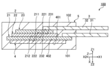
- FIG. 1 is a plan view showing an ultrasonic probe according to a first embodiment
- FIG. 2 is a cross-sectional view of the ultrasonic probe shown in FIG. 1
- FIG. It is a figure which shows the flow of the manufacturing method of the ultrasonic probe of 1st Embodiment.
- FIG. 5 is a plan view showing an ultrasonic probe of a second embodiment
- FIG. 5 is a diagram of the ultrasonic probe of FIG. 4 viewed in the X2 direction
- FIG. 5 is a diagram of the ultrasonic probe of FIG. 4 viewed in the Y1 direction;
- FIG. 1 is a plan view showing the ultrasonic probe 100 of the first embodiment.
- FIG. 2 is a cross-sectional view of the ultrasonic probe 100 shown in FIG. Note that the dimensions and scale of each part of the ultrasonic probe 100 shown in FIG. 2 are appropriately different from the actual ones, and are schematically shown for easy understanding. The thickness of the ultrasound probe 100 is actually much thinner than shown in FIG. Also, FIG. 2 corresponds to the AA line cross section in FIG.
- the X-axis, Y-axis and Z-axis that are orthogonal to each other will be used as appropriate.
- one direction along the X-axis will be referred to as the X1 direction, and the direction opposite to the X1 direction will be referred to as the X2 direction.
- one direction along the Y axis is denoted as Y1 direction, and the opposite direction to Y1 direction is denoted as Y2 direction.
- One direction along the Z-axis is referred to as the Z1 direction, and the direction opposite to the Z1 direction is referred to as the Z2 direction.
- viewing in the Z1 direction or the Z2 direction is referred to as “planar view”.
- the Z1 direction is defined as upward
- the Z2 direction is defined as downward.
- the ultrasonic probe 100 shown in FIGS. 1 and 2 is used for ultrasonic measurement such as medical diagnosis of a living body and non-destructive inspection of structures.
- Ultrasonic measurement is a method of measuring the presence or absence or position of an object by transmitting an ultrasonic signal from the ultrasonic probe 100 toward the object and receiving the ultrasonic signal reflected by the object with the ultrasonic probe 100.
- Ultrasonic waves have the property of being reflected at interfaces between different objects. The greater the difference in acoustic impedance between objects, the greater the reflectance of ultrasonic waves.
- the presence or location of an object is measured based on the reflectance. According to such ultrasonic measurement, the internal structure can be inspected noninvasively and nondestructively.
- the ultrasonic probe 100 has flexibility. This flexible ultrasonic probe 100 has excellent adhesion to curved surfaces such as the neck, chest, abdomen, arms and fingers. Therefore, the ultrasonic probe 100 has excellent adhesion not only to the flat surface of the object but also to the curved surface. By using such an ultrasonic probe 100, the measurable range of an object can be expanded.
- the ultrasonic probe 100 has a piezoelectric element 2 , a flexible wiring board 3 , a backing material 4 and a housing 5 . As shown in FIG. 2, the ultrasonic probe 100 has a lower surface 101 and an upper surface 102 . The top surface 102 is the surface that contacts the object. The ultrasonic probe 100 transmits and receives ultrasonic waves from an upper surface 102 .
- Piezoelectric element 2 The piezoelectric element 2 shown in FIGS. 1 and 2 transmits and receives ultrasonic waves.
- the piezoelectric element 2 has a function of interconverting an electrical signal due to a voltage change and a mechanical vibration of an ultrasonic wave.
- the piezoelectric element 2 has a lower electrode 21 , a piezoelectric body 22 and an upper electrode 23 .
- a piezoelectric body 22 is positioned between and contacts the lower electrode 21 and the upper electrode 23 .
- the lower electrode 21 is located farther from the object than the upper electrode 23 is.
- the lower electrode 21 is another electrode that contacts the surface of the piezoelectric body 22 opposite to the upper electrode 23 .
- the shape of the lower electrode 21 in plan view is a quadrangle.
- the lower electrode 21 has flexibility.
- the material of the lower electrode 21 is, for example, metal such as stainless steel. Since the material of the lower electrode 21 is metal, the lower electrode 21 is thinner than, for example, an elastomer, and the minimum practical hardness of the ultrasonic probe 100 can be ensured.
- the material of the lower electrode 21 may be a metal other than stainless steel, or may be a nonmetallic material such as carbon.
- the lower electrode 21 has a lower surface 211 and an upper surface 212 .
- the piezoelectric body 22 is in contact with the upper surface 212 .
- the thickness of the lower electrode 21 is, for example, preferably 10 ⁇ m or more and 200 ⁇ m or less, and more preferably 50 ⁇ m or more and 100 ⁇ m or less. When the thickness is within the above range, loss of flexibility of the ultrasonic probe 100 is suppressed while ensuring the minimum practical hardness of the ultrasonic probe 100 compared to when the thickness is out of the range.
- the shape of the piezoelectric body 22 in plan view is substantially circular.
- the shape may be a shape other than a circle, for example, a polygon such as a quadrangle.
- the plane area of the piezoelectric body 22 is smaller than the plane area of the lower electrode 21 .
- the piezoelectric body 22 overlaps the lower electrode 21 in plan view.
- the piezoelectric body 22 is a sol-gel film formed by a sol-gel method. Such a piezoelectric body 22 is porous. By forming the piezoelectric body 22 by the sol-gel method, the piezoelectric body 22 having excellent flexibility can be obtained. Examples of the material of the piezoelectric body 22 include piezoelectric ceramics such as lead zirconate titanate (PZT).
- PZT lead zirconate titanate
- the piezoelectric body 22 has a lower surface 221 and an upper surface 222.
- the bottom surface 221 contacts the bottom electrode 21 and the top surface 222 contacts the top electrode 23 .
- the thickness of the piezoelectric body 22 is preferably, for example, 10 ⁇ m or more and 200 ⁇ m or less, and more preferably 50 ⁇ m or more and 100 ⁇ m or less. When the thickness is within the above range, it is easier to deform the piezoelectric body 22 and to form the piezoelectric body 22 by a sol-gel method than when the thickness is outside the range.
- the shape of the upper electrode 23 in plan view is substantially circular.
- the shape may be a shape other than a circle, for example, a polygon such as a quadrangle.
- the plane area of the upper electrode 23 is smaller than the plane area of the lower electrode 21 and the plane area of the piezoelectric body 22 .
- the upper electrode 23 overlaps the lower electrode 21 and the piezoelectric body 22 in plan view.
- the upper electrode 23 is an electrode containing a conductive elastomer.
- the conductive elastomer preferably contains a binder and a conductive filler. Binders include rubbers such as silicone rubbers and urethane rubbers, or thermoplastic elastomers. Examples of conductive fillers include metal particles such as silver powder, conductive carbon, and plated fillers such as silver-plated fillers. The conductive filler may be powdery, particulate, or fibrous.
- the upper electrode 23 contains a conductive elastomer, the upper electrode 23 is a thin film and has excellent flexibility. Therefore, the ability of the upper electrode 23 to follow the deformation of the piezoelectric body 22 can be enhanced. Moreover, by using a conductive elastomer, the upper electrode 23 having a sufficient thickness can be formed on the upper surface 222 of the piezoelectric body 22 . Therefore, it is possible to provide the flexible ultrasonic probe 100 with good conductivity.
- the upper electrode 23 is excellent in flexibility, even if the upper electrode 23 is bent, a decrease in conductivity of the upper electrode 23 is suppressed. If the upper electrode 23 is a metal film, the flexibility of the material itself is low, so if the curvature of the upper electrode 23 is reduced or if the upper electrode 23 is repeatedly bent, the upper electrode 23 may be damaged. However, since the upper electrode 23 in this embodiment is not a metal film and is excellent in flexibility, even when the curvature of the upper electrode 23 is reduced or when the upper electrode 23 is repeatedly bent, the risk of damage such as cracks occurring in the upper electrode 23 can be reduced. Therefore, the decrease in conductivity due to the occurrence of minute cracks in the upper electrode 23 is suppressed. Therefore, the durability of the ultrasonic probe 100 can be improved by including the conductive elastomer in the upper electrode 23 .
- the conductive elastomer preferably contains silicone rubber. Silicone rubber has a low attenuation of ultrasonic waves. For this reason, by using silicone rubber for the upper electrode 23, it is possible to provide the ultrasonic probe 100 with higher precision than when using urethane rubber, for example.
- silver fillers are particularly preferable as the conductive filler.
- a silica core using silica as a core material is exemplified as a silver-plated filler.
- Silver has excellent electrical conductivity. Therefore, by using the silver filler as the conductive filler, it is possible to provide the upper electrode 23 with excellent conductivity.
- the conductive filler may contain, for example, two or more fillers having different average particle diameters. In particular, the performance of the upper electrode 23 can be improved by including two or more kinds of silver fillers having different average particle diameters in the upper electrode 23 .
- the compounding ratio of the conductive filler to 100 phr of the binder is not particularly limited, but is preferably 50 phr or more and 600 phr or less, more preferably 100 phr or more and 400 phr or less. When the compounding ratio is within the above range, it is easier to form the upper electrode 23 that has excellent conductivity and is less likely to be damaged than when it is outside the range.
- the average diameter of the two conductive fillers is not particularly limited, but one is preferably 4 ⁇ m or more and 8 ⁇ m or less, and the other is preferably 5 ⁇ m or more and 15 ⁇ m or less.
- the average diameter is equal to or greater than the above lower limit, the conductive filler is less likely to agglomerate than when it is less than the lower limit.
- the average diameter is equal to or less than the upper limit, the upper electrode 23 is less likely to be damaged by bending with a small curvature, compared to the case where the upper limit is exceeded.
- the conductive elastomer may contain a curing agent and a dispersant in addition to the binder and conductive filler described above. In addition, other materials than those described above may be included to the extent that the characteristics of the upper electrode 23 are not significantly changed.
- the compounding ratio of the curing agent to 100 phr of the binder is, for example, 10 phr or less.
- the compounding ratio of the dispersant to 100 phr of the binder is, for example, 20 phr or less.
- each of the curing agent and the dispersing agent may be used in combination of two or more.
- the upper electrode 23 has a lower surface 231 and an upper surface 232 .
- the lower surface 231 is in contact with the piezoelectric body 22 .
- the upper surface 232 is in contact with the housing 5 .
- the thickness of the upper electrode 23 is, for example, preferably 5 ⁇ m or more and 200 ⁇ m or less, and more preferably 10 ⁇ m or more and 100 ⁇ m or less. When the thickness is within the above range, the upper electrode 23 can be easily deformed, the attenuation of ultrasonic waves can be suppressed, and the thickness of the upper electrode 23 can be easily made uniform, compared to when the thickness is outside the range.
- the piezoelectric element 2 has a flexible lower electrode 21, a piezoelectric body 22 formed by the sol-gel method, and an upper electrode 23 containing a conductive elastomer. Therefore, the piezoelectric element 2 has flexibility. Since the piezoelectric element 2 has flexibility, the flexibility of the ultrasonic probe 100 can be ensured. Therefore, the ultrasonic probe 100 can be applied not only to flat surfaces of objects but also to curved surfaces. Therefore, the applicable range of the ultrasonic probe 100 can be expanded. Furthermore, since the piezoelectric element 2 is excellent in flexibility, damage such as cracks is less likely to occur, so the durability of the ultrasonic probe 100 can be improved.
- Flexible wiring board 3 A flexible wiring board 3 is connected to the piezoelectric element 2 .
- the flexible wiring board 3 has a film-like insulating substrate, wiring 31 arranged in the insulating substrate, and wiring 32 arranged in the insulating substrate. Note that the wirings 31 and 32 are schematically shown in FIG. Also, the insulating substrate is made of resin such as polyimide, for example.
- the wirings 31 and 32 are made of metal such as copper.
- the wiring 31 is connected to the lower electrode 21 .
- the wiring 32 is connected to the upper electrode 23 .
- the backing material 4 is arranged below the lower electrode 21 . Also, the backing material 4 contacts the lower surface 211 of the lower electrode 21 , which is the surface opposite to the piezoelectric body 22 .
- the backing material 4 has flexibility.
- the backing material 4 attenuates the ultrasonic waves radiated downward from the piezoelectric element 2 and suppresses unnecessary vibrations. Since the presence of the backing material 4 can suppress excessive vibration, the resolution can be improved compared to the case without the backing material 4 . In addition, the presence of the backing material 4 reduces multiple reflections between the lower surface 101 of the ultrasonic probe 100 and the lower surface 211 of the piezoelectric element 2 .
- the shape of the backing material 4 in plan view is quadrangular in the illustrated example.
- the shape of the backing material 4 in plan view may be a shape other than a square, for example, a circle.
- the planar area of the backing material 4 is larger than the planar area of the piezoelectric body 22, and the backing material 4 overlaps the piezoelectric body 22 in plan view. Since the plane area of the backing material 4 is larger than the plane area of the piezoelectric body 22, the function of attenuating the ultrasonic waves emitted downward from the piezoelectric body 22 can be effectively exhibited compared to the case where the plane area of the backing material 4 is smaller.
- the material of the backing material 4 is preferably an elastomer. Since the material is an elastomer, the flexibility of the backing material 4 can be ensured.
- the material of the backing material 4 is preferably butyl rubber. Butyl rubber has a greater attenuation of ultrasonic waves than, for example, silicone rubber. Therefore, since the material of the backing material 4 is butyl rubber, ultrasonic waves can be sufficiently attenuated even if the thickness is small.
- the backing material 4 does not contain inorganic particles. By not containing inorganic particles, the flexibility of the backing material 4 can be increased compared to the case where the backing material 4 contains inorganic particles.
- the backing material 4 has a lower surface 401 and an upper surface 402.
- the bottom surface 401 is in contact with the housing 5 .
- the top surface 402 is in contact with the piezoelectric element 2 .
- the thickness of the backing material 4 is preferably, for example, 0.1 mm or more and 1.0 mm or less, and more preferably 0.2 mm or more and 0.8 mm or less. When the thickness is within the above range, the backing material 4 is particularly excellent in flexibility, and the function of the backing material 4 to attenuate ultrasonic waves is exhibited particularly effectively, compared to the case where the thickness is outside the range.
- housing 5 A housing 5 shown in FIG. 1 covers the piezoelectric element 2 and the backing material 4 . A part of the flexible wiring board 3 is located inside the housing 5 and the remaining part is exposed from the housing 5 . Moreover, the housing 5 has flexibility. The housing 5 has a function of protecting the piezoelectric element 2 and the like.
- the material of the housing 5 is preferably elastomer. Since the material is elastomer, the housing 5 is excellent in flexibility, shock absorption, and waterproofness to protect the piezoelectric element 2 . Moreover, as the material of the housing 5, it is preferable to use an elastomer with low attenuation of ultrasonic waves. Since the housing 5 contains an elastomer with low attenuation of ultrasonic waves, the housing 5 functions as an acoustic matching layer in addition to the function of protecting the piezoelectric element 2 and the like.
- the acoustic matching layer is used to reduce the reflection of ultrasonic waves caused by the difference in acoustic impedance between the piezoelectric element 2 and the object.
- the piezoelectric element 2 and the living body have greatly different acoustic impedances. Therefore, the presence of the housing 5 functioning as an acoustic matching layer can reduce the reflection of ultrasonic waves caused by the difference in acoustic impedance between the piezoelectric element 2 and the living body. Therefore, the housing 5 functions as an acoustic matching layer, thereby improving the matching of acoustic impedance and increasing the transmission amount of ultrasonic waves to the object.
- the material of the housing 5 is specifically silicone rubber. Silicone rubber has a smaller attenuation of ultrasonic waves than urethane rubber or the like. Therefore, by including silicone rubber in the housing 5, the housing 5 can be suitably used as an acoustic matching layer.
- the housing 5 contains silicone rubber, so that the housing 5 can function as an acoustic lens if it has an appropriate shape. Acoustic lenses are used to focus ultrasonic waves and improve resolution. Therefore, the existence of the housing 5 functioning as an acoustic lens can improve the resolution compared to the case where the housing 5 does not exist.
- silicone rubber has excellent biocompatibility and is easily applied to medical diagnosis of a living body.
- the acoustic impedance of silicone rubber is close to that of a living body. Therefore, when the object is a living body, the amount of ultrasonic waves that pass through the object can be increased by using silicone rubber, and the resolution can be improved. Further, when the upper electrode 23 contains silicone rubber, the housing 5 also contains silicone rubber, so that the adhesion therebetween can be enhanced.
- the housing 5 does not contain inorganic particles.
- the flexibility of the housing 5 can be increased compared to the case of including inorganic particles.
- each material of the housing 5 and the above-described backing material 4 is an elastomer that does not contain inorganic particles, the flexibility of the ultrasonic probe 100 is less likely to be impaired. Therefore, the adhesiveness to each part of the living body becomes particularly high, and a wide range of diagnosis of the living body is possible.
- the shape of the housing 5 in plan view is a quadrangle in the illustrated example.
- the shape of the housing 5 in a plan view may be a shape other than a square, for example, a circle.
- the plane area of the housing 5, that is, the plane area of the ultrasonic probe 100 is not particularly limited, but is, for example, 50 mm 2 or more and 10000 mm 2 or less.
- the lower surface 101 of the ultrasonic probe 100 corresponds to the lower surface of the housing 5, and the upper surface 102 corresponds to the upper surface of the housing 5.
- the thickness of the ultrasonic probe 100 is, for example, preferably 0.1 mm or more and 10 mm or less, and more preferably 0.5 mm or more and 2 mm or less. When the thickness is within the above range, it is possible to provide the ultrasonic probe 100 which is superior in flexibility and easy to handle as compared with the case where the thickness is out of the range.
- FIG. 3 is a diagram showing the flow of a method for manufacturing the ultrasonic probe 100 of the first embodiment.
- the method of manufacturing the ultrasonic probe 100 includes a piezoelectric element forming step S10, a wiring forming step S20, a backing material forming step S30, and a housing forming step S40.
- the piezoelectric element forming step S10 includes a lower electrode preparing step S11, a piezoelectric body forming step S12, and an upper electrode forming step S13.
- the piezoelectric element 2 is formed. Specifically, first, in the lower electrode preparation step S11, the lower electrode 21 is prepared. Specifically, for example, a stainless steel substrate having a thickness of 50 ⁇ m is prepared.
- the piezoelectric body 22 is formed on the lower electrode 21 by a sol-gel method.
- the piezoelectric body 22 is formed by the sol-gel method.
- the flexible and thin piezoelectric body 22 can be easily formed.
- a sol-gel film having a thickness of about 100 ⁇ m is formed on the lower electrode 21 .
- the upper electrode 23 is formed by applying a conductive elastomer onto the piezoelectric body 22 by, for example, a screen method and curing it.
- a conductive elastomer onto the piezoelectric body 22 by, for example, a screen method and curing it.
- the conductive elastomer is applied on the piezoelectric body 22 to a thickness of 50 ⁇ m or more and 100 ⁇ m or less, and cured at 150° C. for 30 minutes. Further, when the conductive elastomer is applied in a substantially circular shape in plan view, the diameter is, for example, about 6 mm or more and 9 mm or less.
- the conductive elastomer By using the conductive elastomer, the conductive elastomer can be applied onto the piezoelectric body 22 without the material of the upper electrode 23 penetrating into the piezoelectric body 22 . Moreover, by using a conductive elastomer, the upper electrode 23 having a sufficient thickness can be formed on the piezoelectric body 22 . Therefore, the ultrasonic probe 100 with good conductivity can be obtained.
- the conductive elastomer contains a binder, which is rubber such as silicone rubber and urethane rubber, or a thermoplastic elastomer, and a conductive filler. Hardening of the binder prevents movement of the conductive filler.
- the piezoelectric element 2 is formed through the above steps. As described above, the piezoelectric element 2 has the piezoelectric body 22 formed by the sol-gel method and the upper electrode 23 formed using a conductive elastomer. Therefore, the piezoelectric element 2 has flexibility. Since the piezoelectric element 2 has flexibility, the flexibility of the ultrasonic probe 100 can be ensured. Therefore, the ultrasonic probe 100 can be applied not only to flat surfaces of objects but also to curved surfaces. Therefore, the applicable range of the ultrasonic probe 100 can be expanded. Furthermore, since the ultrasonic probe 100 is excellent in flexibility, damage such as cracks is less likely to occur, so the durability of the ultrasonic probe 100 can be improved.
- the flexible wiring board 3 connected to the piezoelectric element 2 is formed.
- the flexible wiring board 3 has a portion where a conductive member such as copper is exposed.
- a conductive member such as copper
- an anisotropic conductive film that functions as an adhesive member is temporarily pressure-bonded to the portion. More specifically, for example, an anisotropic conductive film “MF-331” manufactured by Hitachi Chemical Co., Ltd. is temporarily pressure-bonded at 80° C. for 3 seconds to an exposed copper portion of 1.5 mm square.
- the wiring 32 of the flexible wiring board 3 and the upper electrode 23 are thermocompression bonded.
- the upper electrode 23 is made of silicone rubber, it is preferable to irradiate the surface of the upper electrode 23 with ultraviolet rays to modify the surface and then perform thermocompression bonding. Specifically, for example, the surface of the upper electrode 23 is modified by irradiating vacuum ultraviolet light for 30 seconds using an excimer lamp.
- the wiring 32 and the upper electrode 23 are thermocompression bonded at 140° C. for 10 seconds using an FPC alignment thermocompression bonding apparatus.
- the wiring 31 of the flexible wiring board 3 and the lower electrode 21 are thermocompression bonded. Specifically, for example, the wiring 31 and the lower electrode 21 are thermocompression bonded at 140° C. for 10 seconds using an FPC alignment thermocompression bonding apparatus.
- the backing material 4 is formed. Specifically, the backing material 4 is formed on the lower surface 211 by crimping the backing material 4 onto the lower surface 211 of the lower electrode 21 .
- the backing material 4 contains butyl rubber and the housing 5 contains silicone rubber
- the housing 5 is formed.
- the housing 5 is formed by bonding a sheet containing a self-adhesive elastomer to the top surface 232 of the upper electrode 23 and the bottom surface 401 of the backing material 4 using an adhesive.
- a sheet of self-adhesive silicone rubber is adhered to each of the upper surface 232 and the lower surface 401 using an adhesive.
- the thickness of the sheet in contact with the upper surface 232 of the upper electrode 23 is thinner than the thickness of the sheet in contact with the lower surface 401 of the backing material 4 in consideration of the transmission amount of ultrasonic waves to the object.
- a sheet of self-adhesive silicone rubber having a thickness of 0.4 mm is adhered to the upper surface 232 and a sheet of self-adhesive silicone rubber having a thickness of 0.6 mm is adhered to the lower surface 401 .
- the housing 5 when the housing 5 is formed using a sheet containing silicone rubber, it is preferable to bond the sheets after irradiating the surface of the sheet with ultraviolet rays to modify the surface, since the silicone rubber is difficult to adhere.
- the surface of the sheet is modified by irradiating vacuum ultraviolet light for 30 seconds using an excimer lamp.
- the bonding temperature between the sheet on the upper surface 232 and the sheet on the lower surface 401 is room temperature
- the pressure is 1.2 MPa
- the bonding time is 30 minutes.
- pressure may be applied through the foam sheet. Also, for example, after the sheets are adhered together, they are left to stand for about 24 hours so that they have practical strength.
- the ultrasonic probe 100 is manufactured. According to the method described above, the flexible ultrasonic probe 100 with good resolution can be easily manufactured.
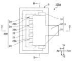
- FIG. 4 is a plan view showing the ultrasonic probe 100A of the second embodiment.
- FIG. 5 is a diagram of the ultrasonic probe 100A of FIG. 4 as viewed in the X2 direction.
- FIG. 6 is a diagram of the ultrasonic probe 100A of FIG. 4 viewed in the Y1 direction. 4, 5 and 6, the dimensions and scale of each part of the ultrasonic probe 100A shown in FIGS. 5 corresponds to the BB line section of FIG.
- FIG. 6 corresponds to the CC line section of FIG.
- the ultrasonic probe 100A of the second embodiment differs from the ultrasonic probe 100 of the first embodiment in having a plurality of piezoelectric elements 2A.
- the ultrasonic probe 100A has a piezoelectric structure 200, a flexible wiring board 3, a backing material 4, and a housing 5.
- the piezoelectric structure 200 includes a plurality of piezoelectric elements 2A.
- the ultrasonic probe 100A has seven piezoelectric elements 2A, but the number of piezoelectric elements 2A is not limited to this, and may be two or more and six or less, or eight or more.
- the ultrasonic probe 100A has a large number of piezoelectric elements 2A, such as 128.
- the piezoelectric structure 200 has a lower electrode 21, a piezoelectric body 22 and a plurality of upper electrodes 23A.
- the lower electrode 21 is integrally provided in common with the plurality of piezoelectric elements 2A.
- the piezoelectric body 22 is integrally provided in common with the plurality of piezoelectric elements 2A.
- the plurality of upper electrodes 23A correspond to "plurality of electrodes".
- the plurality of upper electrodes 23A are provided in one-to-one correspondence with the plurality of piezoelectric elements 2A.
- the shape of each upper electrode 23A in a plan view is a quadrangular shape. Note that the shape may be a polygon other than a quadrangle, or a circle.
- the plurality of upper electrodes 23A are spaced apart from each other and arranged in a row along the Y-axis in plan view.
- the center-to-center distance of the plurality of upper electrodes 23A, that is, the pitch is not particularly limited, but is, for example, about 0.5 mm.
- the plurality of upper electrodes 23A may not be arranged in a line as shown in FIG. 4, but may be arranged in a plurality of rows, or may be randomly arranged.
- the wiring 31 is connected to the lower electrode 21 and the wiring 32 is connected to the plurality of upper electrodes 23 .
- this embodiment has a plurality of piezoelectric elements 2A.
- a plurality of upper electrodes 23A are provided in one-to-one correspondence with the plurality of piezoelectric elements 2A, and the piezoelectric body 22 is integrally provided in common with the plurality of piezoelectric elements 2A. Therefore, only the portion of the piezoelectric body 22 to which the voltage is applied can be vibrated.
- the piezoelectric body 22 is formed by a sol-gel method and is porous and thin.
- the piezoelectric body 22 is flexible because it is formed by the sol-gel method, and is integrally provided in common with the plurality of piezoelectric elements 2A. For this reason, it is excellent in the ability to follow the bending of a curved object.
- a plurality of piezoelectric elements 2A are required to display an image of the ultrasonic probe 100 for medical use.
- having a plurality of piezoelectric elements 2A allows the ultrasonic probe 100 to be used as a phased array probe.
- the method for manufacturing the ultrasonic probe 100A includes steps shown in FIG.
- the lower electrode 21 is prepared. Specifically, for example, a stainless steel substrate having a plane area of 25 mm ⁇ 84 mm and a thickness of 50 ⁇ m is prepared.
- the piezoelectric body 22 is formed on the lower electrode 21 by a sol-gel method. Specifically, for example, a sol-gel film having a plane area of 15 mm ⁇ 80 mm and a thickness of about 100 ⁇ m is formed on the lower electrode 21 .
- the sol-gel film is the piezoelectric body 22 .
- the upper electrode 23 is formed by applying a conductive elastomer onto the piezoelectric body 22 by, for example, a screen method and curing it.
- a conductive elastomer is applied on the piezoelectric body 22 and cured at 150° C. for 30 minutes.
- the conductive elastomer is applied in a rectangular pattern having a plane area of 4.5 mm ⁇ 0.25 mm and a thickness of about 50 ⁇ m.
- 128 rectangular patterns are formed. 128 rectangular patterns are formed at a pitch of 0.5 mm, for example.
- the flexible ultrasonic probe 100A with good resolution can be easily manufactured.
- the ultrasonic probe 100 may be an array probe.
Landscapes
- Health & Medical Sciences (AREA)
- Engineering & Computer Science (AREA)
- Life Sciences & Earth Sciences (AREA)
- Physics & Mathematics (AREA)
- Chemical & Material Sciences (AREA)
- General Health & Medical Sciences (AREA)
- Pathology (AREA)
- Manufacturing & Machinery (AREA)
- Mechanical Engineering (AREA)
- General Physics & Mathematics (AREA)
- Biochemistry (AREA)
- Immunology (AREA)
- Analytical Chemistry (AREA)
- Dispersion Chemistry (AREA)
- Heart & Thoracic Surgery (AREA)
- Veterinary Medicine (AREA)
- Molecular Biology (AREA)
- Surgery (AREA)
- Animal Behavior & Ethology (AREA)
- Biomedical Technology (AREA)
- Public Health (AREA)
- Medical Informatics (AREA)
- Acoustics & Sound (AREA)
- Radiology & Medical Imaging (AREA)
- Nuclear Medicine, Radiotherapy & Molecular Imaging (AREA)
- Biophysics (AREA)
- Gynecology & Obstetrics (AREA)
- Ceramic Engineering (AREA)
- Transducers For Ultrasonic Waves (AREA)
Priority Applications (4)
| Application Number | Priority Date | Filing Date | Title |
|---|---|---|---|
| EP23743161.4A EP4468743A4 (en) | 2022-01-19 | 2023-01-12 | ULTRASONIC PROBE AND METHOD FOR MANUFACTURING ULTRASONIC PROBE |
| CN202380016896.XA CN118661431A (zh) | 2022-01-19 | 2023-01-12 | 超声波探头和用于制造超声波探头的方法 |
| US18/728,973 US20250169367A1 (en) | 2022-01-19 | 2023-01-12 | Ultrasonic probe and method for manufacturing ultrasonic probe |
| JP2023575215A JPWO2023140166A1 (https=) | 2022-01-19 | 2023-01-12 |
Applications Claiming Priority (4)
| Application Number | Priority Date | Filing Date | Title |
|---|---|---|---|
| JP2022-006067 | 2022-01-19 | ||
| JP2022006067 | 2022-01-19 | ||
| JP2022151759 | 2022-09-22 | ||
| JP2022-151759 | 2022-09-22 |
Publications (1)
| Publication Number | Publication Date |
|---|---|
| WO2023140166A1 true WO2023140166A1 (ja) | 2023-07-27 |
Family
ID=87348787
Family Applications (1)
| Application Number | Title | Priority Date | Filing Date |
|---|---|---|---|
| PCT/JP2023/000563 Ceased WO2023140166A1 (ja) | 2022-01-19 | 2023-01-12 | 超音波プローブおよび超音波プローブの製造方法 |
Country Status (4)
| Country | Link |
|---|---|
| US (1) | US20250169367A1 (https=) |
| EP (1) | EP4468743A4 (https=) |
| JP (1) | JPWO2023140166A1 (https=) |
| WO (1) | WO2023140166A1 (https=) |
Citations (10)
| Publication number | Priority date | Publication date | Assignee | Title |
|---|---|---|---|---|
| JP2009210440A (ja) * | 2008-03-04 | 2009-09-17 | Toin Gakuen | 筒型キャビテーションセンサ及びその製造方法 |
| JP2010136807A (ja) * | 2008-12-10 | 2010-06-24 | Konica Minolta Medical & Graphic Inc | 超音波探触子及び超音波探触子の作製方法 |
| JP2011067485A (ja) * | 2009-09-28 | 2011-04-07 | Fujifilm Corp | 超音波トランスデューサ及び超音波プローブ |
| WO2011105269A1 (ja) * | 2010-02-26 | 2011-09-01 | 株式会社 日立メディコ | 超音波探触子とそれを用いた超音波撮像装置 |
| WO2013058237A1 (ja) * | 2011-10-17 | 2013-04-25 | 東海ゴム工業株式会社 | 誘電膜およびそれを用いたトランスデューサ |
| WO2013063676A1 (en) | 2010-11-05 | 2013-05-10 | National Research Council Of Canada | Ultrasonic transducer assembly and system for monitoring structural integrity |
| WO2013150667A1 (ja) * | 2012-04-05 | 2013-10-10 | Necトーキン株式会社 | 圧電素子、圧電振動モジュールおよびそれらの製造方法 |
| WO2014119166A1 (ja) * | 2013-01-30 | 2014-08-07 | 東海ゴム工業株式会社 | 柔軟なトランスデューサ |
| WO2018225415A1 (ja) * | 2017-06-09 | 2018-12-13 | 国立大学法人熊本大学 | 基板及び膜基板生産方法 |
| JP2022076783A (ja) * | 2020-11-10 | 2022-05-20 | 天草池田電機株式会社 | 超音波トランスデューサーアレイ、超音波トランスデューサーアレイの製造方法、超音波トランスデューサーアレイを用いたパラメトリックスピーカー及び超音波トランスデューサーアレイを用いたパラメトリックスピーカーの使用方法 |
Family Cites Families (10)
| Publication number | Priority date | Publication date | Assignee | Title |
|---|---|---|---|---|
| JPH02196600A (ja) * | 1989-01-26 | 1990-08-03 | Ngk Spark Plug Co Ltd | 超音波探触子における分割電極の作成方法 |
| JPH067678Y2 (ja) * | 1989-02-03 | 1994-02-23 | 日本特殊陶業株式会社 | ピエゾゴム超音波探触子 |
| JP3560998B2 (ja) * | 1993-01-27 | 2004-09-02 | 株式会社東芝 | 圧電材料および超音波プローブ |
| JPH08126090A (ja) * | 1994-10-27 | 1996-05-17 | Kanebo Ltd | 水中超音波受信素子製造に係る防水保護膜形成法 |
| JP5905192B2 (ja) * | 2010-07-30 | 2016-04-20 | コニカミノルタ株式会社 | 超音波探触子の製造方法 |
| JP5802448B2 (ja) * | 2011-06-21 | 2015-10-28 | オリンパス株式会社 | 超音波ユニット、超音波内視鏡および超音波ユニットの製造方法 |
| JP6122066B2 (ja) * | 2015-06-24 | 2017-04-26 | 国立大学法人 熊本大学 | 高周波超音波圧電素子、その製造方法、及びそれを含む高周波超音波プローブ |
| CN107924986B (zh) * | 2015-07-16 | 2021-02-23 | 住友理工株式会社 | 压电传感器 |
| JP2018159708A (ja) * | 2017-03-23 | 2018-10-11 | 積水化学工業株式会社 | 荷重検出装置 |
| JPWO2020075212A1 (ja) * | 2018-10-08 | 2021-10-21 | 住友理工株式会社 | 胸骨圧迫訓練用人形 |
-
2023
- 2023-01-12 US US18/728,973 patent/US20250169367A1/en active Pending
- 2023-01-12 EP EP23743161.4A patent/EP4468743A4/en active Pending
- 2023-01-12 WO PCT/JP2023/000563 patent/WO2023140166A1/ja not_active Ceased
- 2023-01-12 JP JP2023575215A patent/JPWO2023140166A1/ja active Pending
Patent Citations (10)
| Publication number | Priority date | Publication date | Assignee | Title |
|---|---|---|---|---|
| JP2009210440A (ja) * | 2008-03-04 | 2009-09-17 | Toin Gakuen | 筒型キャビテーションセンサ及びその製造方法 |
| JP2010136807A (ja) * | 2008-12-10 | 2010-06-24 | Konica Minolta Medical & Graphic Inc | 超音波探触子及び超音波探触子の作製方法 |
| JP2011067485A (ja) * | 2009-09-28 | 2011-04-07 | Fujifilm Corp | 超音波トランスデューサ及び超音波プローブ |
| WO2011105269A1 (ja) * | 2010-02-26 | 2011-09-01 | 株式会社 日立メディコ | 超音波探触子とそれを用いた超音波撮像装置 |
| WO2013063676A1 (en) | 2010-11-05 | 2013-05-10 | National Research Council Of Canada | Ultrasonic transducer assembly and system for monitoring structural integrity |
| WO2013058237A1 (ja) * | 2011-10-17 | 2013-04-25 | 東海ゴム工業株式会社 | 誘電膜およびそれを用いたトランスデューサ |
| WO2013150667A1 (ja) * | 2012-04-05 | 2013-10-10 | Necトーキン株式会社 | 圧電素子、圧電振動モジュールおよびそれらの製造方法 |
| WO2014119166A1 (ja) * | 2013-01-30 | 2014-08-07 | 東海ゴム工業株式会社 | 柔軟なトランスデューサ |
| WO2018225415A1 (ja) * | 2017-06-09 | 2018-12-13 | 国立大学法人熊本大学 | 基板及び膜基板生産方法 |
| JP2022076783A (ja) * | 2020-11-10 | 2022-05-20 | 天草池田電機株式会社 | 超音波トランスデューサーアレイ、超音波トランスデューサーアレイの製造方法、超音波トランスデューサーアレイを用いたパラメトリックスピーカー及び超音波トランスデューサーアレイを用いたパラメトリックスピーカーの使用方法 |
Non-Patent Citations (1)
| Title |
|---|
| See also references of EP4468743A4 |
Also Published As
| Publication number | Publication date |
|---|---|
| EP4468743A4 (en) | 2026-01-07 |
| US20250169367A1 (en) | 2025-05-22 |
| EP4468743A1 (en) | 2024-11-27 |
| JPWO2023140166A1 (https=) | 2023-07-27 |
Similar Documents
| Publication | Publication Date | Title |
|---|---|---|
| US8408063B2 (en) | Ultrasonic probe, and ultrasonic diagnostic apparatus using the same | |
| EP2014236A1 (en) | Ultrasonic probe | |
| US20130085396A1 (en) | Ultrasonic probe and ultrasonic display device | |
| JP2012135622A (ja) | 超音波探触子及びこれを用いた超音波診断装置 | |
| JP2014146885A (ja) | 超音波デバイス、超音波プローブ、電子機器および超音波画像装置 | |
| JPWO2004091255A1 (ja) | 超音波振動子及びその製造方法 | |
| JP5406374B2 (ja) | 超音波探触子およびそれを用いた超音波診断装置 | |
| CN104545993A (zh) | 超声波器件、超声波探头、超声波探测器及电子设备 | |
| CN109387562B (zh) | 超声波装置 | |
| US10429497B2 (en) | Ultrasonic device, ultrasonic probe, electronic apparatus, and ultrasonic imaging apparatus | |
| CN111558514B (zh) | 一种超声换能器 | |
| JP2005177479A (ja) | 小型素子超音波トランスデューサ・アレイ用の音響裏当て材 | |
| WO2023140166A1 (ja) | 超音波プローブおよび超音波プローブの製造方法 | |
| CN102105784A (zh) | 检测设备 | |
| JP6277899B2 (ja) | 超音波振動子、超音波探触子および超音波撮像装置 | |
| CN116197102B (zh) | 一种超声换能器 | |
| CN118661431A (zh) | 超声波探头和用于制造超声波探头的方法 | |
| US7898154B2 (en) | Ultrasound probe and method for manufacturing the same | |
| JP2012257058A (ja) | 超音波振動子及び超音波診断装置 | |
| CN108209964A (zh) | 超声波探头 | |
| CN118594896A (zh) | 行列寻址的柔性面阵超声换能器阵列及其制备方法 | |
| JP2012244273A (ja) | 超音波探触子 | |
| WO2020203317A1 (ja) | 超音波放射器具及び超音波装置 | |
| JP2010258602A (ja) | 超音波探触子およびその製造方法 | |
| CN113588795A (zh) | 柔性超声面阵的制作方法、柔性超声面阵及超声成像方法 |
Legal Events
| Date | Code | Title | Description |
|---|---|---|---|
| 121 | Ep: the epo has been informed by wipo that ep was designated in this application |
Ref document number: 23743161 Country of ref document: EP Kind code of ref document: A1 |
|
| WWE | Wipo information: entry into national phase |
Ref document number: 202380016896.X Country of ref document: CN |
|
| WWE | Wipo information: entry into national phase |
Ref document number: 18728973 Country of ref document: US |
|
| ENP | Entry into the national phase |
Ref document number: 2023575215 Country of ref document: JP Kind code of ref document: A |
|
| WWE | Wipo information: entry into national phase |
Ref document number: 2023743161 Country of ref document: EP |
|
| NENP | Non-entry into the national phase |
Ref country code: DE |
|
| ENP | Entry into the national phase |
Ref document number: 2023743161 Country of ref document: EP Effective date: 20240819 |
|
| WWP | Wipo information: published in national office |
Ref document number: 18728973 Country of ref document: US |