WO2023136183A1 - 反射型マスクブランク、反射型マスク、反射型マスクの製造方法 - Google Patents
反射型マスクブランク、反射型マスク、反射型マスクの製造方法 Download PDFInfo
- Publication number
- WO2023136183A1 WO2023136183A1 PCT/JP2022/048684 JP2022048684W WO2023136183A1 WO 2023136183 A1 WO2023136183 A1 WO 2023136183A1 JP 2022048684 W JP2022048684 W JP 2022048684W WO 2023136183 A1 WO2023136183 A1 WO 2023136183A1
- Authority
- WO
- WIPO (PCT)
- Prior art keywords
- film
- reflective mask
- absorber
- mask blank
- reflective
- Prior art date
- Legal status (The legal status is an assumption and is not a legal conclusion. Google has not performed a legal analysis and makes no representation as to the accuracy of the status listed.)
- Ceased
Links
Images




Classifications
-
- G—PHYSICS
- G03—PHOTOGRAPHY; CINEMATOGRAPHY; ANALOGOUS TECHNIQUES USING WAVES OTHER THAN OPTICAL WAVES; ELECTROGRAPHY; HOLOGRAPHY
- G03F—PHOTOMECHANICAL PRODUCTION OF TEXTURED OR PATTERNED SURFACES, e.g. FOR PRINTING, FOR PROCESSING OF SEMICONDUCTOR DEVICES; MATERIALS THEREFOR; ORIGINALS THEREFOR; APPARATUS SPECIALLY ADAPTED THEREFOR
- G03F1/00—Originals for photomechanical production of textured or patterned surfaces, e.g., masks, photo-masks, reticles; Mask blanks or pellicles therefor; Containers specially adapted therefor; Preparation thereof
- G03F1/22—Masks or mask blanks for imaging by radiation of 100nm or shorter wavelength, e.g. X-ray masks, extreme ultraviolet [EUV] masks; Preparation thereof
- G03F1/24—Reflection masks; Preparation thereof
Definitions
- the present invention relates to a reflective mask used for EUV (Etreme Ultra Violet: Extreme Ultra Violet) exposure used in the exposure process of semiconductor manufacturing, a manufacturing method thereof, and a reflective mask blank that is the original plate of the reflective mask.
- EUV EUV
- the reflective mask has a multilayer reflective film that reflects EUV light formed on a substrate, and an absorber film that absorbs EUV light is patterned on the multilayer reflective film.
- a protective film is often formed between the multilayer reflective film and the absorber film to protect the multilayer reflective film from etching during mask pattern formation (Patent Document 1).
- the EUV light incident on the reflective mask from the illumination optical system of the exposure apparatus is reflected at portions (openings) without the absorber film and absorbed at portions (non-openings) with the absorber film.
- the mask pattern is transferred as a resist pattern onto the wafer through the reduction projection optical system of the exposure apparatus, and subsequent processing is performed.
- the electromagnetic waves emitted from the EUV light source may include ultraviolet light other than EUV light.
- Light in the ultraviolet wavelength range other than the EUV light is called OOB (Out of Band) light.
- Resists used for forming resist patterns often have photosensitivity not only to EUV light but also to OOB light, and in particular, ultraviolet light with a wavelength of 150 to 300 nm (hereinafter also referred to as "resist photosensitive ultraviolet light").
- resist photosensitive ultraviolet light ultraviolet light with a wavelength of 150 to 300 nm
- a multilayer reflective film having a Ru protective film has a reflectance of about 65% for EUV light with a wavelength of about 13.5 nm, and also has a high reflectance for ultraviolet light with a wavelength of 150 nm or more in addition to EUV light.
- the resist-sensitive ultraviolet light When the resist-sensitive ultraviolet light is reflected by the multilayer reflective film in the opening as described above, the resist-sensitive ultraviolet light does not form an image on the wafer during EUV light projection exposure, but exposes the entire resist. It can deteriorate the shape of the resist pattern. Therefore, it has been desired to develop a reflective mask that suppresses the reflection of resist-sensitive ultraviolet light in the opening, ie, the region where the absorber film does not exist. In addition, the reflective mask is required to have high EUV light reflectance.
- Patent Document 1 discloses a reflective mask blank in which a thermal diffusion suppression film is provided between a protective film and a multilayer reflective film.
- the thickness of the thermal diffusion suppressing film is considered to be 0.5 to 2.5 nm, and the reflective mask formed using the mask blank is sufficient to suppress the reflection of resist-sensitive ultraviolet light. I didn't.
- an object of the present invention is to provide a reflective mask blank that suppresses reflection of EUV light and suppresses reflection of resist-sensitive ultraviolet light when the reflective mask is manufactured. do.
- Another object of the present invention is to provide a method of manufacturing a reflective mask using the reflective mask blank, and a reflective mask.
- the present inventors have found that a silicon nitride film, a silicon oxide film, and a silicon oxynitride film having a film thickness of 7 to 11 nm are provided between the multilayer reflective film and the protective film.
- the inventors have found that the above object can be achieved by providing one type of intermediate film selected from the group, and have completed the present invention.
- a reflective mask blank having, on a substrate, a multilayer reflective film that reflects EUV light, an intermediate film, a protective film, and an absorber film in this order,
- the intermediate film is one selected from the group consisting of a silicon nitride film, a silicon oxide film, and a silicon oxynitride film,
- the material constituting the hard mask film is either chromium or silicon, or a material containing chromium and one or more elements selected from the group consisting of oxygen, nitrogen, carbon and hydrogen.
- the reflective mask blank of [1] which is a material containing silicon and one or more elements selected from the group consisting of oxygen, nitrogen, carbon and hydrogen.
- the absorber film is a simple substance of ruthenium metal; One or more elements selected from the group consisting of ruthenium, tantalum, and tin, and the group consisting of chromium, gold, platinum, rhenium, hafnium, titanium, silicon, niobium, oxygen, nitrogen, boron, and hydrogen and one or more selected elements.
- a reflective mask having an absorber film pattern formed by patterning the absorber film of the reflective mask blank according to any one of [1] to [4].
- a method for manufacturing a reflective mask comprising patterning the absorber film of the reflective mask blank according to any one of [1] to [4].
- the present invention it is possible to provide a reflective mask blank that suppresses reflection of EUV light and suppresses reflection of resist-sensitive ultraviolet light when the reflective mask is manufactured. Further, according to the present invention, it is possible to provide a method of manufacturing a reflective mask using a reflective mask blank, and a reflective mask.
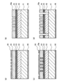
- FIG. 1 is a schematic diagram showing an example of the aspect of the reflective mask blank of this embodiment.
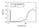
- FIG. 2 is a graph showing the reflectance of a multilayer reflective film quoted from Non-Patent Document 1 at wavelengths of 10 to 400 nm.
- FIG. 3 is a schematic diagram showing an example of the aspect of the reflective mask blank of this embodiment.
- FIGS. 4A and 4B are schematic diagrams showing an example of a manufacturing process of a reflective mask using the reflective mask blank of this embodiment.
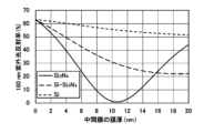
- FIG. 5 is a graph obtained by simulating the reflectance of a laminate having a Ru protective film, an intermediate film and a multilayer reflective film to 180 nm ultraviolet rays.
- FIG. 1 is a schematic diagram showing an example of the aspect of the reflective mask blank of this embodiment.
- FIG. 2 is a graph showing the reflectance of a multilayer reflective film quoted from Non-Patent Document 1 at wavelengths of 10 to 400 nm.
- FIG. 3 is a schematic diagram showing an example of the aspect of
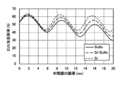
- FIG. 6 is a graph obtained by simulating the EUV light reflectance of a laminate having a Ru protective film, an intermediate film, and a multilayer reflective film.
- FIG. 7 is a graph obtained by simulating the reflectance of a laminate having an Rh protective film, an intermediate film, and a multilayer reflective film to 180 nm ultraviolet rays.
- FIG. 8 is a graph obtained by simulating the EUV light reflectance of a laminate having an Rh protective film, an intermediate film, and a multilayer reflective film.
- a numerical range represented by "to” means a range including the numerical values before and after “to” as lower and upper limits.
- elements such as hydrogen, boron, carbon, nitrogen, oxygen, fluorine, silicon, chlorine, titanium, chromium, niobium, ruthenium, rhodium, tin, hafnium, tantalum, platinum, gold, etc. have corresponding element symbols (H, B, C, N, O, F, Si, Cl, Ti, Cr, Nb, Ru, Rh, Sn, Hf, Ta, Pt, Au, etc.).
- the reflective mask blank of this embodiment has, on a substrate, a multilayer reflective film that reflects EUV light, an intermediate film, a protective film, and an absorber film in this order.
- the intermediate film is one selected from the group consisting of a silicon nitride film, a silicon oxide film, and a silicon oxynitride film, and the thickness of the intermediate film is 7 to 11 nm.
- FIG. 1 is a cross-sectional view showing an example of the aspect of the reflective mask blank of this embodiment.
- the reflective mask blank 10 shown in FIG. 1 has a substrate 11 , a multilayer reflective film 12 , an intermediate film 13 , a protective film 14 , and an absorber film 15 in this order. It has a back conductive film 16 on the side surface.
- the reflective mask blank 10 shown in FIG. 1 has a rear conductive film 16, it may have no rear conductive film 16.
- the reflective mask blank 10a of this embodiment comprises a substrate 11, a multilayer reflective film 12, an intermediate film 13, a protective film 14, an absorber film 15, and a hard mask film 17 in this order. and a rear conductive film 16 on the surface of the substrate 11 opposite to the multilayer reflective film 12 .
- the reflective mask blank 10a shown in FIG. 3 has the back conductive film 16, the back conductive film 16 may not be provided.
- resist photosensitive ultraviolet light (with a wavelength of 150 to 300 nm) is applied. UV light) can be reflected. It is considered that the reflected light of the resist photosensitive ultraviolet light from the reflective mask is generated at the exposed surface of the protective film 14 and the multilayer reflective film 12 (mainly at the interface with the intermediate film 13).
- the intermediate film 13 has the above aspect, since the intermediate film is transparent to the resist-sensitive ultraviolet light, the reflected light beams of the resist-sensitive ultraviolet light produced above interfere with each other, and the reflection is suppressed. At the same time, when the intermediate film 13 has the above aspect, the EUV light reflectance of the multilayer reflective film 12 can be maintained.
- the configuration of the reflective mask blank of this embodiment will be described below.
- a reflective mask when a reflective mask is manufactured, suppression of reduction in reflection of EUV light in a region where there is no absorber film (region where the protective film is exposed) is referred to as “excellent EUV light reflectance. ” is also called.
- excellent EUV light reflectance when a reflective mask is manufactured, the fact that the reflection of the resist photosensitive ultraviolet light is suppressed in the region where the absorber film is not present (the region where the protective film is exposed) is referred to as the “low reflectivity of the resist photosensitive ultraviolet light”. It is also said to be superior to
- the substrate included in the reflective mask blank of this embodiment preferably has a small coefficient of thermal expansion.
- the coefficient of thermal expansion of the substrate is preferably 0 ⁇ 1.0 ⁇ 10 -7 /°C, more preferably 0 ⁇ 0.3 ⁇ 10 -7 /°C at 20°C.
- Materials with a small thermal expansion coefficient include, but are not limited to, SiO 2 —TiO 2 -based glasses, and substrates such as crystallized glass in which a ⁇ -quartz solid solution is precipitated, quartz glass, metallic silicon, and metals. can also be used.
- the SiO 2 —TiO 2 -based glass it is preferable to use quartz glass containing 90 to 95% by mass of SiO 2 and 5 to 10% by mass of TiO 2 .
- the content of TiO 2 is 5 to 10% by mass, the coefficient of linear expansion near room temperature is approximately zero, and dimensional change hardly occurs near room temperature.
- the SiO 2 —TiO 2 -based glass may contain trace components other than SiO 2 and TiO 2 .
- the surface of the substrate on which the multilayer reflective film is laminated (hereinafter also referred to as "first main surface") preferably has high surface smoothness.
- the surface smoothness of the first main surface can be evaluated by surface roughness.
- the surface roughness of the first main surface is preferably 0.15 nm or less in terms of root-mean-square roughness Rq.
- the surface roughness can be measured with an atomic force microscope, and the surface roughness is described as the root-mean-square roughness Rq based on JIS B0601:2013.
- the first main surface is preferably surface-processed so as to have a predetermined flatness in order to improve the pattern transfer accuracy and positional accuracy of the reflective mask obtained using the reflective mask blank.
- the substrate preferably has a flatness of 100 nm or less, more preferably 50 nm or less, and even more preferably 30 nm or less in a predetermined area (for example, a 132 mm ⁇ 132 mm area) of the first main surface.
- the flatness can be measured by, for example, a plane measuring interferometer manufactured by Fujifilm Corporation.
- the size, thickness and the like of the substrate are appropriately determined according to the design values of the mask and the like.
- the outer shape may be 6 inches (152 mm) square and the thickness may be 0.25 inches (6.3 mm).
- the substrate preferably has high rigidity in order to prevent deformation due to film stress of films (multilayer reflective film, absorber film, etc.) formed on the substrate.
- the Young's modulus of the substrate is preferably 65 GPa or more.
- the multilayer reflective film that the reflective mask blank of this embodiment has is not particularly limited as long as it has the desired properties as the reflective layer of the EUV mask blank.
- the multilayer reflective film preferably has a high reflectance with respect to EUV light. is preferably 60% or more, more preferably 65% or more.
- the maximum reflectance for EUV light near a wavelength of 13.5 nm is preferably 60% or more, more preferably 65% or more. .
- the multilayer reflective film can achieve a high EUV light reflectance, it usually includes a high refractive index layer that exhibits a high refractive index for EUV light and a low refractive index layer that exhibits a low refractive index for EUV light.
- a multi-layer reflective film is used which is alternately laminated a plurality of times.
- the multilayer reflective film may be laminated for a plurality of periods with a laminated structure in which a high refractive index layer and a low refractive index layer are laminated in this order from the substrate side as one period.
- a lamination structure in which layers are laminated in order may be regarded as one period, and a plurality of periods may be laminated.
- a layer containing Si can be used as the high refractive index layer.
- a Si compound containing Si and at least one selected from the group consisting of B, C, N, and O can be used.
- a reflective mask having excellent EUV light reflectance can be obtained.
- a layer containing a metal selected from the group consisting of Mo, Ru, Rh, and Pt, or an alloy thereof can be used as the low refractive index layer.
- Si is widely used for the high refractive index layer
- Mo is widely used for the low refractive index layer. That is, Mo/Si multilayer reflective films are the most common.
- the multilayer reflective film is not limited thereto, and Ru/Si multilayer reflective film, Mo/Be multilayer reflective film, Mo compound/Si compound multilayer reflective film, Si/Mo/Ru multilayer reflective film, Si/Mo/Ru/ A Mo multilayer reflective film and a Si/Ru/Mo/Ru multilayer reflective film can also be used.
- each layer constituting the multilayer reflective film and the number of layer repeating units can be appropriately selected according to the film material used and the EUV light reflectance required for the reflective layer.
- a Mo/Si multilayer reflective film as an example, a Mo film with a thickness of 2.3 ⁇ 0.1 nm and a film thickness of 4 A Si film having a thickness of 0.5 ⁇ 0.1 nm may be laminated so that the number of repeating units is 30 to 60.
- Each layer constituting the multilayer reflective film can be formed to a desired thickness using a known film forming method such as magnetron sputtering or ion beam sputtering.
- a known film forming method such as magnetron sputtering or ion beam sputtering.
- ion beam sputtering is used to produce a multilayer reflective film
- ion particles are supplied from an ion source to a high refractive index material target and a low refractive index material target.
- the multilayer reflective film is a Mo/Si multilayer reflective film
- an Si layer having a predetermined thickness is formed on the substrate by ion beam sputtering, for example, using a Si target. After that, using a Mo target, a Mo layer having a predetermined film thickness is formed.
- a Mo/Si multilayer reflective film is formed by stacking 30 to 60 cycles of the Si layer and the Mo layer as one cycle.
- the layer in contact with the intermediate film of the multilayer reflective film is preferably made of a material that is difficult to oxidize.
- a layer made of a material that is resistant to oxidation functions as a cap layer for the multilayer reflective film.
- a layer made of a material that is difficult to oxidize includes a Si layer.
- the intermediate film included in the reflective mask blank of the present embodiment is one selected from the group consisting of a silicon nitride film, a silicon oxide film, and a silicon oxynitride film, and the thickness of the intermediate film is 7 to 11 nm. is.
- the intermediate film is a silicon nitride film
- the intermediate film is a film containing Si and N
- a film containing Si and N is preferable.
- the molar ratio of Si 3 N 4 to Si in the Si—Si 3 N 4 film is preferably 0.25-4.00, more preferably 0.43-1.50.
- x in the SiN x film is preferably 0.1 to 1.0, more preferably 0.2 to 0.5.
- the silicon nitride film may contain elements other than Si and N, excluding O.
- the intermediate film is a silicon oxide film
- the intermediate film is a film containing Si and O, and a film containing Si and O is preferable.
- the molar ratio of SiO 2 to Si in the Si—SiO 2 film is preferably 0.67-9.00, more preferably 1.50-4.00.
- the x in the SiO x film is preferably 0.4 to 1.6, more preferably 0.7 to 1.3.
- the silicon oxide film may contain elements other than Si and O, excluding N.
- the intermediate film is a silicon oxynitride film
- the intermediate film is a film containing Si, O and N, and a film containing Si, O and N is preferable.
- the molar ratio of Si 2 N 2 O to Si in the Si—Si 2 N 2 O film is preferably 0.25 to 4.00, more preferably 0.43 to 2.33.
- x in the SiO x N y film is preferably 0.05 to 0.3, more preferably 0.1 to 0.2.
- y in the SiO x N y film is preferably 0.1 to 0.6, more preferably 0.2 to 0.5.
- the silicon oxynitride film may contain elements other than Si, O and N.
- the film thickness of the intermediate film is 7 to 11 nm.
- the film thickness of the intermediate film is preferably 7.5 to 10.5 nm, more preferably 8 to 10 nm.
- the film thickness of the intermediate film can be obtained by preparing a cross section of a reflective mask blank and analyzing the cross section by a scanning transmission electron microscope-energy dispersive X-ray spectroscopy (STEM-EDS) method.
- the intermediate film is preferably transparent to the resist-sensitive ultraviolet light from the viewpoint of excellent low reflectivity of the resist-sensitive ultraviolet light.
- the intermediate film is transparent to the resist-sensitive ultraviolet light, the resist-sensitive ultraviolet light from the multilayer reflective film and the protective film can interfere with each other, and the low reflectivity of the resist-sensitive ultraviolet light is excellent.
- transparent to resist-sensitive ultraviolet light means that the transmittance of the resist-sensitive ultraviolet light is 30% or more, and the transmittance is preferably 50% or more, and 70% or more. is more preferred.
- the intermediate film preferably does not reduce the high EUV light reflectance exhibited by the multilayer reflective film. In this respect, the intermediate film preferably has high EUV light transmittance.
- the intermediate film is preferably a silicon nitride film or a silicon oxynitride film, more preferably a silicon nitride film, because of its high EUV light transmittance.
- the crystalline state of the intermediate film may be either crystalline or non-crystalline, preferably non-crystalline.
- the intermediate film can be formed to a desired thickness using known film forming methods such as magnetron sputtering and ion beam sputtering.
- film forming methods such as magnetron sputtering and ion beam sputtering.
- ion particles are supplied from an ion source to a Si target, and nitrogen gas is contained in the film forming atmosphere.
- An intermediate film of a silicon oxide film or a silicon oxynitride film can be formed by changing the type of gas contained in the film forming atmosphere. Further, by changing the amount and ratio of gases contained in the film-forming atmosphere, the ratio of each element contained in the intermediate film can be adjusted.
- the protective film of the reflective mask blank of the present embodiment is a multilayer reflective film that prevents the multilayer reflective film from being damaged by the etching process when patterning the absorber film by an etching process (usually a dry etching process). provided for the purpose of protecting
- the protective film preferably contains at least one element selected from the group consisting of Ru and Rh. More specifically, as the material, Ru metal simple substance, Ru alloy containing one or more metals selected from the group consisting of Ru and Si, Ti, Nb, Rh, Ta, and Zr, Ru Ru-based materials such as Ru-containing nitrides containing alloys and nitrogen, and one or more metals selected from the group consisting of simple Rh metal, Rh, and Si, Ti, Nb, Rh, Ta, and Zr Rh-based materials such as Rh alloys containing and Rh-containing nitrides containing the above Rh alloys and nitrogen.
- Examples of materials that can achieve the above object include Cr, Al, Ta, nitrides containing these metals and nitrogen, and Al 2 O 3 .
- Ru-based materials or Rh-based materials are preferable as materials capable of achieving the above object, and Ru metal simple substance, Ru alloy, Rh metal simple substance, or Rh alloy are more preferable.
- Ru alloys are preferably Ru—Si alloys, and Rh alloys are preferably Rh—Si alloys.
- the Ru content in the Ru alloy is preferably 30 at % or more and less than 100 at %.
- the protective film is made of a Rh alloy, the Rh content in the Rh alloy is preferably 30 at % or more and less than 100 at %. If the Ru content or Rh content is within the above range, the protective film can function as an etching stopper when the absorber film is etched, while sufficiently ensuring the reflectance of EUV light. Furthermore, it is possible to impart washing resistance to the reflective mask and prevent deterioration over time of the multilayer reflective film.
- the film thickness of the protective film is not particularly limited as long as it can function as a protective film. From the viewpoint of maintaining the reflectance of EUV light reflected by the multilayer reflective film, the film thickness of the protective film is preferably 1 to 10 nm, more preferably 1.5 to 6 nm, and even more preferably 2 to 5 nm. It is also preferable that the material of the protective film is Ru metal simple substance, Ru alloy, Rh metal simple substance, or Rh alloy, and that the film thickness of the protective film is the preferable film thickness described above.
- the film thickness of the protective film can be obtained by preparing a cross section of a reflective mask blank and analyzing the cross section by a scanning transmission electron microscope-energy dispersive X-ray spectroscopy (STEM-EDS) method.
- STEM-EDS scanning transmission electron microscope-energy dispersive X-ray spectroscopy
- the protective film can be deposited using a well-known deposition method such as magnetron sputtering or ion beam sputtering.
- a well-known deposition method such as magnetron sputtering or ion beam sputtering.
- magnetron sputtering it is preferable to use a Ru target as the target and Ar gas as the sputtering gas.
- the absorber film included in the reflective mask blank of the present embodiment is required to have a high contrast between the EUV light reflected by the multilayer reflective film and the EUV light by the absorber film when the absorber film is patterned. be done.
- a patterned absorber film may absorb EUV light and function as a binary mask, reflecting the EUV light and interfering with the EUV light from the multilayer reflective film to produce contrast. It may also function as a phase shift mask for increasing the thickness.
- the absorber film is made of Ru metal alone, or one or more elements selected from the group consisting of Ru, Ta, and Sn, and Cr, Au, Pt, Re, and one or more elements selected from the group consisting of Hf, Ti, Si, Nb, O, N, B, and H.
- the above embodiment can use an absorber film pattern, which will be described later, as a binary mask or a phase shift mask.
- the absorber film When the absorber film pattern is used as a binary mask, the absorber film needs to absorb EUV light and have a low EUV light reflectance. Specifically, when the surface of the absorber film is irradiated with EUV light, the maximum value of the reflectance of EUV light around a wavelength of 13.5 nm is desirably 2% or less.
- the absorber film contains at least one element selected from the group consisting of Ta, Ti, Sn and Cr and at least one element selected from the group consisting of O, N, B, Hf and H. may contain Among these, N or B is preferably included. By containing N or B, the crystalline state of the absorber film can be changed to an amorphous or microcrystalline structure.
- the crystalline state of the absorber film is preferably amorphous. This can improve the smoothness and flatness of the absorber film. Further, when the smoothness and flatness of the absorber film are increased, the edge roughness of the absorber film pattern is reduced, and the dimensional accuracy of the absorber film pattern can be increased.
- the EUV light reflectance of the absorber film is preferably 2% or more.
- the absorber film preferably has a reflectance of 9 to 15%. Using an absorber film as a phase shift mask improves the contrast of the optical image on the wafer and increases the exposure margin.
- Materials for forming the phase shift mask include, for example, Ru metal element, Ru alloy containing Ru and one or more metals selected from the group consisting of Cr, Au, Pt, Re, Hf, Ti and Si, Ta and Nb, oxides containing Ru alloys or TaNb alloys and oxygen, nitrides containing Ru alloys or TaNb alloys and nitrogen, oxynitrides containing Ru alloys or TaNb alloys, oxygen and nitrogen, etc. be done.
- the material for forming the phase shift mask is selected to be different from the material for forming the protective film.
- the absorber film may be a single layer film or a multilayer film consisting of a plurality of films.
- the absorber film is a single-layer film, the number of steps in manufacturing the mask blank can be reduced, and production efficiency can be improved.
- the absorber film is a multilayer film, the layer arranged on the side opposite to the protective film side of the absorber film has a reflection during the absorber film pattern inspection using inspection light (for example, a wavelength of 193 to 248 nm). It may be a protective film.
- the absorber film can be formed using a known film formation method such as magnetron sputtering or ion beam sputtering.
- a Ru oxide film is formed as the absorber film by magnetron sputtering
- the absorber film can be formed by sputtering using a Ru target and supplying gas containing Ar gas and oxygen gas.
- the reflective mask blank of this embodiment may have a back conductive film on the surface (second main surface) opposite to the first main surface of the substrate.
- the back conductive film preferably has a low sheet resistance value.
- the sheet resistance value of the back conductive film is, for example, preferably 200 ⁇ / ⁇ or less, more preferably 100 ⁇ / ⁇ or less.
- the constituent material of the back conductive film can be widely selected from those described in known literatures. For example, a high dielectric constant coating described in Japanese Patent Publication No. 2003-501823, specifically a coating made of Si, Mo, Cr, CrON, or TaSi can be applied.
- the constituent material of the back conductive film is a Cr compound containing Cr and one or more selected from the group consisting of B, N, O, and C, or Ta and B, N, O, and C It may be a Ta compound containing one or more selected from the group consisting of
- the thickness of the back conductive film is preferably 10 to 1000 nm, more preferably 10 to 400 nm.
- the back conductive film may have a function of adjusting the stress on the second main surface side of the reflective mask blank. In other words, the back conductive film can be adjusted to flatten the reflective mask blank by balancing the stress from various films formed on the first main surface side.
- the back surface conductive film can be formed using a known film forming method, for example, a sputtering method such as a magnetron sputtering method or an ion beam sputtering method, a CVD method, a vacuum deposition method, or an electrolytic plating method.
- a sputtering method such as a magnetron sputtering method or an ion beam sputtering method
- CVD method a vacuum deposition method
- electrolytic plating method electrolytic plating method
- the reflective mask blank of this embodiment may have other films.
- Other films include hard mask films.
- the hard mask film is preferably arranged on the side of the absorber film opposite to the protective film side.
- a material having high resistance to dry etching such as a Cr-based film and a Si-based film, is preferably used.
- Specific examples of materials for the hard mask film include any one of chromium (Cr) and silicon (Si), Cr, and one or more elements selected from the group consisting of O, N, C, and H. or a material containing Si and one or more elements selected from the group consisting of O, N, C, and H.
- a reflective mask is obtained by patterning an absorber film of a reflective mask blank. That is, the reflective mask blank of this embodiment has an absorber film pattern formed by patterning the absorber film of the reflective mask blank of this embodiment.
- FIG. 4A An example of a method of manufacturing a reflective mask will be described with reference to FIGS. 4(a) to 4(b).
- a resist pattern 18 is formed on a reflective mask blank having a back conductive film 16, a substrate 11, a multilayer reflective film 12, an intermediate film 13, a protective film 14, and an absorber film 15 in this order. It shows the formed state.
- a known method can be used to form the resist pattern 18. For example, a resist is applied onto the absorber film 15 of the reflective mask blank, and the resist pattern 18 is formed by exposure and development. The resist pattern 18 corresponds to a pattern formed on the wafer using a reflective mask. Thereafter, using the resist pattern 18 of FIG.
- the absorber film 15 is etched and patterned, and the resist pattern 18 is removed to form the absorber film pattern 15a shown in FIG. 4(b).
- a laminate is obtained.
- a resist pattern 19 corresponding to the frame of the exposure region is formed on the laminate in FIG. 4(b), and the resist pattern 19 in FIG. 4(c) is used as a mask. Dry etching is performed as Dry etching is performed until the substrate 11 is reached. After dry etching, the resist pattern 19 is removed to obtain the reflective mask shown in FIG. 4(d).
- Dry etching for forming the absorber film pattern 15a includes, for example, dry etching using a Cl-based gas and dry etching using an F-based gas.
- the removal of the resist pattern 18 or 19 may be performed by a known method, such as removal with a cleaning liquid.
- the cleaning liquid include sulfuric acid-hydrogen peroxide aqueous solution (SPM), sulfuric acid, ammonia water, ammonia-hydrogen peroxide aqueous solution (APM), OH radical cleaning water, and ozone water.
- the reflective mask obtained by patterning the absorber film of the reflective mask blank of the present embodiment can be suitably applied as a reflective mask used for exposure with EUV light.
- the reflective mask of the present embodiment suppresses reflection of resist photosensitive ultraviolet light from the openings of the absorber film pattern (regions where the absorber film does not exist) and has a high EUV light reflectance.
- a resist pattern can be formed on a wafer without deteriorating the shape of the resist pattern provided on the wafer.
- a reflective mask blank having, on a substrate, a multilayer reflective film that reflects EUV light, an intermediate film, a protective film, and an absorber film in this order,
- the intermediate film is one selected from the group consisting of a silicon nitride film, a silicon oxide film, and a silicon oxynitride film,
- ⁇ 2> having a hard mask film on the side opposite to the protective film side of the absorber film;
- the material constituting the hard mask film is either chromium or silicon, or a material containing chromium and one or more elements selected from the group consisting of oxygen, nitrogen, carbon and hydrogen.
- the reflective mask blank according to ⁇ 1> which is a material containing silicon and one or more elements selected from the group consisting of oxygen, nitrogen, carbon and hydrogen.
- the absorber film is a simple substance of ruthenium metal, One or more elements selected from the group consisting of ruthenium, tantalum, and tin, and the group consisting of chromium, gold, platinum, rhenium, hafnium, titanium, silicon, niobium, oxygen, nitrogen, boron, and hydrogen
- ⁇ 4> The reflective mask blank according to any one of ⁇ 1> to ⁇ 3>, wherein the protective film contains at least one element selected from the group consisting of ruthenium and rhodium.
- ⁇ 6> A method for manufacturing a reflective mask, comprising patterning the absorber film of the reflective mask blank according to any one of ⁇ 1> to ⁇ 4>.
- Examplementation of simulation> A simulation was performed under the conditions shown below.
- the complex refractive index in the EUV light region is quoted from the database (https://henke.lbl.gov/optical_constants) provided by CXRO (The Center for X-Ray Optics).
- the complex refractive index in the ultraviolet region is obtained from a database provided by Angstrom Sun Technologies (http://www.angstec.com/database) and RefractiveIndex. Quoted from the INFO database (https://refractiveindex.info/).
- the material of the protective film is Ru metal alone, the film thickness of the protective film is 2.4 nm, and the intermediate film is Si film, Si 3 N 4 film, and Si—Si 3 N 4 film (Si and Si 3 N 4 film).
- FIG. 5 shows the dependence of reflectance of ultraviolet light with a wavelength of 180 nm on the film thickness of the intermediate film when the mixture film and the molar ratio of Si 3 N 4 to Si is 1.00).
- Example 1 is a Si film
- Example 2 is a Si 3 N 4 film
- Example 3 is a Si—Si 3 N 4 film.
- Example 1 is a comparative example, and Examples 2 and 3 are examples.
- FIG. 6 shows the dependence of the reflectance of EUV light with a wavelength of 13.5 nm on the film thickness of the intermediate film. The UV light with a wavelength of 180 nm is included in the resist photosensitive UV light.
- the reflective mask blank of the present embodiment suppresses the reduction of reflection of EUV light and achieves suppression of reflection of resist-sensitive ultraviolet light when a reflective mask is manufactured. It can be said.
- FIG. 7 shows the dependence of the reflectance of the intermediate film on the film thickness of the intermediate film of a Si film, a Si 3 N 4 film, and a Si—Si 3 N 4 film, for ultraviolet light having a wavelength of 180 nm.
- Example 4 is a Si film
- Example 5 is a Si 3 N 4 film
- Example 6 is a Si—Si 3 N 4 film.
- Example 4 is a comparative example, and Examples 5 and 6 are examples.
- FIG. 8 shows the dependence of the reflectance of EUV light with a wavelength of 13.5 nm on the film thickness of the intermediate film.
- the reflective mask blank of the present embodiment suppresses the reduction of reflection of EUV light and achieves suppression of reflection of resist-sensitive ultraviolet light when a reflective mask is manufactured. It can be said.
- Reference Signs List 10 10a reflective mask blank 11 substrate 12 multilayer reflective film 13 intermediate film 14 protective film 15 absorber film 15a absorber film pattern 16 rear conductive film 17 hard mask film 18, 19 resist pattern
Landscapes
- Physics & Mathematics (AREA)
- General Physics & Mathematics (AREA)
- Preparing Plates And Mask In Photomechanical Process (AREA)
- Laminated Bodies (AREA)
Abstract
本発明は、基板上に、EUV光を反射する多層反射膜と、中間膜と、保護膜と、吸収体膜とをこの順に有する反射型マスクブランクであって、中間膜が、シリコン窒化膜、シリコン酸化膜、および、シリコン酸窒化膜からなる群から選択される1種であり、中間膜の膜厚が、7~11nmである、反射型マスクブランクに関する。
Description
本発明は、半導体製造の露光プロセスで使用されるEUV(Etreme Ultra Violet:極端紫外)露光に用いられる反射型マスクおよびその製造方法、ならびに、反射型マスクの原板である反射型マスクブランクに関する。
近年、半導体デバイスの更なる微細化のために、光源として中心波長13.5nm付近のEUV光を使用したEUVリソグラフィが検討されている。
EUV露光では、EUV光の特性から、反射光学系ならびに反射型マスクが用いられる。反射型マスクは、基板上にEUV光を反射する多層反射膜が形成され、多層反射膜上にEUV光を吸収する吸収体膜がパターニングされている。多層反射膜と吸収体膜の間には、マスクパターンを形成する際のエッチングから多層反射膜を保護するための保護膜が形成されることも多い(特許文献1)。
露光装置の照明光学系より反射型マスクに入射したEUV光は、吸収体膜の無い部分(開口部)では反射され、吸収体膜の有る部分(非開口部)では吸収される。結果として、マスクパターンが露光装置の縮小投影光学系を通してウエハ上にレジストパターンとして転写され、その後の処理が実施される。
一方、EUV光の光源から発せられる電磁波には、EUV光以外の紫外光も含まれ得る。上記EUV光以外の紫外光波長域の光は、OOB(Out of Band)光と呼ばれている。レジストパターンの形成に用いるレジストは、EUV光だけでなく上記OOB光にも感光性を有することが多く、特に、波長150~300nmの紫外光(以下、「レジスト感光性紫外光」ともいう。)に対する感光性が高い。
非開口部におけるレジスト感光性紫外光の反射率は、上記吸収体膜上に低反射膜を設けることで低下させることができるが、開口部においては、多層反射膜によってレジスト感光性紫外光の反射が発生し得る。図2に、非特許文献1より引用した、Ru保護膜を有する多層反射膜の波長10~400nmにおける反射率を示す。Ru保護膜を有する多層反射膜は波長13.5nm付近のEUV光で65%程度の反射率を持つ一方、EUV光以外に波長150nm以上の紫外光でも反射率が大きい。
非開口部におけるレジスト感光性紫外光の反射率は、上記吸収体膜上に低反射膜を設けることで低下させることができるが、開口部においては、多層反射膜によってレジスト感光性紫外光の反射が発生し得る。図2に、非特許文献1より引用した、Ru保護膜を有する多層反射膜の波長10~400nmにおける反射率を示す。Ru保護膜を有する多層反射膜は波長13.5nm付近のEUV光で65%程度の反射率を持つ一方、EUV光以外に波長150nm以上の紫外光でも反射率が大きい。
S.A.George他、Proc.SPIE 巻7636、763626(2010)
上記のような開口部における、多層反射膜によるレジスト感光性紫外光の反射が発生すると、レジスト感光性紫外光は、EUV光の投影露光時にウエハ上で結像しないものの、レジスト全体を露光してレジストパターンの形状を悪化させ得る。
したがって、開口部、すなわち吸収体膜が存在しない領域における、レジスト感光性紫外光の反射が抑制された反射型マスクの開発が望まれていた。
また、反射型マスクは、EUV光の反射率が高いことが求められる。
したがって、開口部、すなわち吸収体膜が存在しない領域における、レジスト感光性紫外光の反射が抑制された反射型マスクの開発が望まれていた。
また、反射型マスクは、EUV光の反射率が高いことが求められる。
特許文献1では、保護膜と多層反射膜との間に熱拡散抑制膜を設けた反射型マスクブランクが開示されている。上記熱拡散抑制膜の膜厚は、0.5~2.5nmが適当とされており、上記マスクブランクを用いて形成された反射型マスクでは、レジスト感光性紫外光の反射の抑制が十分でなかった。
そこで、本発明は、反射型マスクを作製した際に、EUV光の反射の低減が抑制され、かつ、レジスト感光性紫外光の反射の抑制が達成される、反射型マスクブランクの提供を課題とする。
また、本発明は、上記反射型マスクブランクを用いた反射型マスクの製造方法、および、反射型マスクの提供も課題とする。
また、本発明は、上記反射型マスクブランクを用いた反射型マスクの製造方法、および、反射型マスクの提供も課題とする。
本発明者らは、上記課題について鋭意検討した結果、多層反射膜と保護膜との間に、膜厚が7~11nmである、シリコン窒化膜、シリコン酸化膜、および、シリコン酸窒化膜からなる群から選択される1種の中間膜を設けることにより、上記課題が達成されることを見出し、本発明を完成させるに至った。
すなわち、発明者らは、以下の構成により上記課題が解決できることを見出した。
〔1〕 基板上に、EUV光を反射する多層反射膜と、中間膜と、保護膜と、吸収体膜とをこの順に有する反射型マスクブランクであって、
上記中間膜が、シリコン窒化膜、シリコン酸化膜、および、シリコン酸窒化膜からなる群から選択される1種であり、
上記中間膜の膜厚が、7~11nmである、反射型マスクブランク。
〔2〕 上記吸収体膜の上記保護膜側とは反対側にハードマスク膜を有し、
上記ハードマスク膜を構成する材料が、クロムおよびシリコンのいずれかの材料であるか、クロムと、酸素、窒素、炭素および水素からなる群から選択される1種以上の元素とを含む材料であるか、シリコンと、酸素、窒素、炭素および水素からなる群から選択される1種以上の元素とを含む材料である、〔1〕に記載の反射型マスクブランク。
〔3〕 上記吸収体膜が、ルテニウム金属単体であるか、
ルテニウム、タンタル、および、スズからなる群から選択される1種以上の元素と、クロム、金、白金、レニウム、ハフニウム、チタン、シリコン、ニオブ、酸素、窒素、ホウ素、および、水素からなる群から選択される1種以上の元素とを含む、〔1〕に記載の反射型マスクブランク。
〔4〕 上記保護膜が、ルテニウム、および、ロジウムからなる群から選択される少なくとも1つの元素を含む、〔1〕に記載の反射型マスクブランク。
〔5〕 〔1〕~〔4〕のいずれか1つに記載の反射型マスクブランクの上記吸収体膜をパターニングして形成される吸収体膜パターンを有する反射型マスク。
〔6〕 〔1〕~〔4〕のいずれか1つに記載の反射型マスクブランクの上記吸収体膜をパターニングする工程を含む、反射型マスクの製造方法。
〔1〕 基板上に、EUV光を反射する多層反射膜と、中間膜と、保護膜と、吸収体膜とをこの順に有する反射型マスクブランクであって、
上記中間膜が、シリコン窒化膜、シリコン酸化膜、および、シリコン酸窒化膜からなる群から選択される1種であり、
上記中間膜の膜厚が、7~11nmである、反射型マスクブランク。
〔2〕 上記吸収体膜の上記保護膜側とは反対側にハードマスク膜を有し、
上記ハードマスク膜を構成する材料が、クロムおよびシリコンのいずれかの材料であるか、クロムと、酸素、窒素、炭素および水素からなる群から選択される1種以上の元素とを含む材料であるか、シリコンと、酸素、窒素、炭素および水素からなる群から選択される1種以上の元素とを含む材料である、〔1〕に記載の反射型マスクブランク。
〔3〕 上記吸収体膜が、ルテニウム金属単体であるか、
ルテニウム、タンタル、および、スズからなる群から選択される1種以上の元素と、クロム、金、白金、レニウム、ハフニウム、チタン、シリコン、ニオブ、酸素、窒素、ホウ素、および、水素からなる群から選択される1種以上の元素とを含む、〔1〕に記載の反射型マスクブランク。
〔4〕 上記保護膜が、ルテニウム、および、ロジウムからなる群から選択される少なくとも1つの元素を含む、〔1〕に記載の反射型マスクブランク。
〔5〕 〔1〕~〔4〕のいずれか1つに記載の反射型マスクブランクの上記吸収体膜をパターニングして形成される吸収体膜パターンを有する反射型マスク。
〔6〕 〔1〕~〔4〕のいずれか1つに記載の反射型マスクブランクの上記吸収体膜をパターニングする工程を含む、反射型マスクの製造方法。
本発明によれば、反射型マスクを作製した際に、EUV光の反射の低減が抑制され、かつ、レジスト感光性紫外光の反射の抑制が達成される、反射型マスクブランクを提供できる。
また、本発明によれば、反射型マスクブランクを用いた反射型マスクの製造方法、および、反射型マスクも提供できる。
また、本発明によれば、反射型マスクブランクを用いた反射型マスクの製造方法、および、反射型マスクも提供できる。
以下、本発明について詳細に説明する。
以下に記載する構成要件の説明は、本発明の代表的な実施態様に基づいてなされる場合があるが、本発明はそのような実施態様に制限されない。
本明細書における各記載の意味を示す。
本明細書において、「~」を用いて表される数値範囲は、「~」の前後に記載される数値を下限値および上限値として含む範囲を意味する。
本明細書において、水素、ホウ素、炭素、窒素、酸素、フッ素、シリコン、塩素、チタン、クロム、ニオブ、ルテニウム、ロジウム、スズ、ハフニウム、タンタル、白金、金等の元素は、それぞれ対応する元素記号(H、B、C、N、O、F、Si、Cl、Ti、Cr、Nb、Ru、Rh、Sn、Hf、Ta、Ptおよび、Au等)で表す場合がある。
以下に記載する構成要件の説明は、本発明の代表的な実施態様に基づいてなされる場合があるが、本発明はそのような実施態様に制限されない。
本明細書における各記載の意味を示す。
本明細書において、「~」を用いて表される数値範囲は、「~」の前後に記載される数値を下限値および上限値として含む範囲を意味する。
本明細書において、水素、ホウ素、炭素、窒素、酸素、フッ素、シリコン、塩素、チタン、クロム、ニオブ、ルテニウム、ロジウム、スズ、ハフニウム、タンタル、白金、金等の元素は、それぞれ対応する元素記号(H、B、C、N、O、F、Si、Cl、Ti、Cr、Nb、Ru、Rh、Sn、Hf、Ta、Ptおよび、Au等)で表す場合がある。
<反射型マスクブランク>
本実施形態の反射型マスクブランクは、基板上に、EUV光を反射する多層反射膜と、中間膜と、保護膜と、吸収体膜とをこの順に有する。また、中間膜が、シリコン窒化膜、シリコン酸化膜、および、シリコン酸窒化膜からなる群から選択される1種であり、中間膜の膜厚が、7~11nmである。
本実施形態の反射型マスクブランクについて、図面を参照しながら説明する。
本実施形態の反射型マスクブランクは、基板上に、EUV光を反射する多層反射膜と、中間膜と、保護膜と、吸収体膜とをこの順に有する。また、中間膜が、シリコン窒化膜、シリコン酸化膜、および、シリコン酸窒化膜からなる群から選択される1種であり、中間膜の膜厚が、7~11nmである。
本実施形態の反射型マスクブランクについて、図面を参照しながら説明する。
図1は、本実施形態の反射型マスクブランクの態様の一例を示す断面図である。図1に示す反射型マスクブランク10は、基板11、多層反射膜12、中間膜13、保護膜14、および、吸収体膜15をこの順に有し、基板11の多層反射膜12側とは反対側の面に、裏面導電膜16を有する。
図1に示す反射型マスクブランク10は、裏面導電膜16を有する態様だが、裏面導電膜16を有さない態様であってもよい。
また、本実施形態の反射型マスクブランク10aは、図3に示すように、基板11、多層反射膜12、中間膜13、保護膜14、吸収体膜15、および、ハードマスク膜17をこの順に有し、基板11の多層反射膜12とは反対側の面に、裏面導電膜16を有する態様であってもよい。なお、図3に示す反射型マスクブランク10aは、裏面導電膜16を有する態様だが、裏面導電膜16を有さない態様であってもよい。
図1に示す反射型マスクブランク10は、裏面導電膜16を有する態様だが、裏面導電膜16を有さない態様であってもよい。
また、本実施形態の反射型マスクブランク10aは、図3に示すように、基板11、多層反射膜12、中間膜13、保護膜14、吸収体膜15、および、ハードマスク膜17をこの順に有し、基板11の多層反射膜12とは反対側の面に、裏面導電膜16を有する態様であってもよい。なお、図3に示す反射型マスクブランク10aは、裏面導電膜16を有する態様だが、裏面導電膜16を有さない態様であってもよい。
ここで、上記反射型マスクブランク10を用いて吸収体膜15をパターニングして反射型マスクを作製した際に、保護膜14が露出した領域においては、レジスト感光性紫外光(波長150~300nmの紫外光)が反射し得る。
反射型マスクからのレジスト感光性紫外光の反射光は、露出した保護膜14の表面と、多層反射膜12(主に中間膜13との界面)とで生じると考えられる。中間膜13が上記態様である場合、中間膜はレジスト感光性紫外光に対して透明であるため、上記生じたレジスト感光性紫外光の反射光同士が干渉し、反射が抑制される。また、同時に、中間膜13が上記態様である場合、多層反射膜12が有するEUV光の反射率を維持できる。
反射型マスクからのレジスト感光性紫外光の反射光は、露出した保護膜14の表面と、多層反射膜12(主に中間膜13との界面)とで生じると考えられる。中間膜13が上記態様である場合、中間膜はレジスト感光性紫外光に対して透明であるため、上記生じたレジスト感光性紫外光の反射光同士が干渉し、反射が抑制される。また、同時に、中間膜13が上記態様である場合、多層反射膜12が有するEUV光の反射率を維持できる。
以下、本実施形態の反射型マスクブランクが有する構成について説明する。
なお、以下、反射型マスクを作製した際に、吸収体膜がない領域(保護膜が露出した領域)において、EUV光の反射の低減が抑制されることを、「EUV光の反射率に優れる」ともいう。また、反射型マスクを作製した際に、吸収体膜がない領域(保護膜が露出した領域)においてレジスト感光性紫外光の反射が抑制されることを、「レジスト感光性紫外光の低反射性に優れる」ともいう。
なお、以下、反射型マスクを作製した際に、吸収体膜がない領域(保護膜が露出した領域)において、EUV光の反射の低減が抑制されることを、「EUV光の反射率に優れる」ともいう。また、反射型マスクを作製した際に、吸収体膜がない領域(保護膜が露出した領域)においてレジスト感光性紫外光の反射が抑制されることを、「レジスト感光性紫外光の低反射性に優れる」ともいう。
(基板)
本実施形態の反射型マスクブランクが有する基板は、熱膨張係数が小さいことが好ましい。基板の熱膨張係数が小さい方が、EUV光による露光時の熱により、吸収体膜パターンに歪みが生じることを抑制できる。
基板の熱膨張係数は、20℃において、0±1.0×10⁻⁷/℃が好ましく、0±0.3×10-7/℃がより好ましい。
熱膨張係数が小さい材料としては、SiO2-TiO2系ガラス等が挙げられるが、これに限定されず、β石英固溶体を析出した結晶化ガラス、石英ガラス、金属シリコン、および、金属等の基板も使用できる。
SiO2-TiO2系ガラスは、SiO2を90~95質量%、TiO2を5~10質量%含む石英ガラスを用いることが好ましい。TiO2の含有量が5~10質量%であると、室温付近での線膨張係数が略ゼロであり、室温付近での寸法変化がほとんど生じない。なお、SiO2-TiO2系ガラスは、SiO2およびTiO2以外の微量成分を含んでもよい。
本実施形態の反射型マスクブランクが有する基板は、熱膨張係数が小さいことが好ましい。基板の熱膨張係数が小さい方が、EUV光による露光時の熱により、吸収体膜パターンに歪みが生じることを抑制できる。
基板の熱膨張係数は、20℃において、0±1.0×10⁻⁷/℃が好ましく、0±0.3×10-7/℃がより好ましい。
熱膨張係数が小さい材料としては、SiO2-TiO2系ガラス等が挙げられるが、これに限定されず、β石英固溶体を析出した結晶化ガラス、石英ガラス、金属シリコン、および、金属等の基板も使用できる。
SiO2-TiO2系ガラスは、SiO2を90~95質量%、TiO2を5~10質量%含む石英ガラスを用いることが好ましい。TiO2の含有量が5~10質量%であると、室温付近での線膨張係数が略ゼロであり、室温付近での寸法変化がほとんど生じない。なお、SiO2-TiO2系ガラスは、SiO2およびTiO2以外の微量成分を含んでもよい。
基板の多層反射膜が積層される側の面(以下、「第1主面」ともいう。)は、高い表面平滑性を有することが好ましい。第1主面の表面平滑性は、表面粗さで評価できる。第1主面の表面粗さは、二乗平均平方根粗さRqで、0.15nm以下が好ましい。なお、表面粗さは、原子間力顕微鏡で測定でき、表面粗さは、JIS B0601:2013に基づく二乗平均平方根粗さRqとして説明する。
第1主面は、反射型マスクブランクを用いて得られる反射型マスクのパターン転写精度および位置精度を高められる点で、所定の平坦度となるように表面加工されることが好ましい。基板は、第1主面の所定の領域(例えば、132mm×132mmの領域)において、平坦度は、100nm以下が好ましく、50nm以下がより好ましく、30nm以下がさらに好ましい。平坦度は、例えば、富士フイルム社製の平面測定用干渉計によって測定できる。
基板の大きさおよび厚さ等は、マスクの設計値等により適宜決定される。例えば、外形は6インチ(152mm)角、および、厚さは0.25インチ(6.3mm)等が挙げられる。
基板の大きさおよび厚さ等は、マスクの設計値等により適宜決定される。例えば、外形は6インチ(152mm)角、および、厚さは0.25インチ(6.3mm)等が挙げられる。
さらに、基板は、基板上に形成される膜(多層反射膜、吸収体膜等)の膜応力による変形を防止する点で、高い剛性を有することが好ましい。例えば、基板のヤング率は、65GPa以上が好ましい。
(多層反射膜)
本実施形態の反射型マスクブランクが有する多層反射膜は、EUVマスクブランクの反射層として所望の特性を有する限り特に限定されない。多層反射膜は、EUV光に対して高い反射率を有することが好ましく、具体的には、EUV光が入射角6°で多層反射膜の表面に入射した際、波長13.5nm付近のEUV光の反射率の最大値は、60%以上が好ましく、65%以上がより好ましい。また、多層反射膜の上に、保護膜が積層されている場合でも、同様に、波長13.5nm付近のEUV光の反射率の最大値は、60%以上が好ましく、65%以上がより好ましい。
本実施形態の反射型マスクブランクが有する多層反射膜は、EUVマスクブランクの反射層として所望の特性を有する限り特に限定されない。多層反射膜は、EUV光に対して高い反射率を有することが好ましく、具体的には、EUV光が入射角6°で多層反射膜の表面に入射した際、波長13.5nm付近のEUV光の反射率の最大値は、60%以上が好ましく、65%以上がより好ましい。また、多層反射膜の上に、保護膜が積層されている場合でも、同様に、波長13.5nm付近のEUV光の反射率の最大値は、60%以上が好ましく、65%以上がより好ましい。
多層反射膜は、高いEUV光の反射率を達成できることから、通常はEUV光に対して高い屈折率を示す高屈折率層と、EUV光に対して低い屈折率を示す低屈折率層とを交互に複数回積層させた多層反射膜が用いられる。
多層反射膜は、高屈折率層と低屈折率層とを基板側からこの順に積層した積層構造を1周期として複数周期積層してもよいし、低屈折率層と高屈折率層とをこの順に積層した積層構造を1周期として複数周期積層してもよい。
多層反射膜は、高屈折率層と低屈折率層とを基板側からこの順に積層した積層構造を1周期として複数周期積層してもよいし、低屈折率層と高屈折率層とをこの順に積層した積層構造を1周期として複数周期積層してもよい。
高屈折率層としては、Siを含む層を用いることができる。Siを含む材料としては、Si単体の他に、Siに、B、C、N、およびOからなる群から選択される1種以上を含むSi化合物を用いることができる。Siを含む高屈折率層を用いることによって、EUV光の反射率に優れた反射型マスクが得られる。
低屈折率層としては、Mo、Ru、Rh、およびPtからなる群から選択される金属、またはこれらの合金を含む層を用いることができる。
上記高屈折率層には、Siが広く使用され、低屈折率層にはMoが広く使用される。すなわち、Mo/Si多層反射膜が最も一般的である。但し、多層反射膜はこれに限定されず、Ru/Si多層反射膜、Mo/Be多層反射膜、Mo化合物/Si化合物多層反射膜、Si/Mo/Ru多層反射膜、Si/Mo/Ru/Mo多層反射膜、Si/Ru/Mo/Ru多層反射膜も使用できる。
低屈折率層としては、Mo、Ru、Rh、およびPtからなる群から選択される金属、またはこれらの合金を含む層を用いることができる。
上記高屈折率層には、Siが広く使用され、低屈折率層にはMoが広く使用される。すなわち、Mo/Si多層反射膜が最も一般的である。但し、多層反射膜はこれに限定されず、Ru/Si多層反射膜、Mo/Be多層反射膜、Mo化合物/Si化合物多層反射膜、Si/Mo/Ru多層反射膜、Si/Mo/Ru/Mo多層反射膜、Si/Ru/Mo/Ru多層反射膜も使用できる。
多層反射膜を構成する各層の膜厚および層の繰り返し単位の数は、使用する膜材料および反射層に要求されるEUV光の反射率に応じて適宜選択できる。Mo/Si多層反射膜を例にとると、EUV光の反射率の最大値が60%以上の多層反射膜とするには、膜厚2.3±0.1nmのMo膜と、膜厚4.5±0.1nmのSi膜とを繰り返し単位数が30~60になるように積層させればよい。
なお、多層反射膜を構成する各層は、マグネトロンスパッタリング法、イオンビームスパッタリング法等、公知の成膜方法を用いて所望の厚さになるように成膜できる。例えば、イオンビームスパッタリング法を用いて多層反射膜を作製する場合、高屈折率材料のターゲットおよび低屈折率材料のターゲットに対して、イオン源からイオン粒子を供給して行う。多層反射膜がMo/Si多層反射膜である場合、イオンビームスパッタリング法により、例えば、まずSiターゲットを用いて、所定の膜厚のSi層を基板上に成膜する。その後、Moターゲットを用いて、所定の膜厚のMo層を成膜する。このSi層およびMo層を1周期として、30~60周期積層させることにより、Mo/Si多層反射膜が成膜される。
多層反射膜の中間膜と接する層は、酸化されにくい材料からなる層が好ましい。酸化されにくい材料からなる層は、多層反射膜のキャップ層として機能する。酸化されにくい材料からなる層としては、Si層が挙げられる。多層反射膜がSi/Mo多層反射膜である場合、中間膜と接する層をSi層とすると、中間膜と接する層がキャップ層として機能する。その場合キャップ層の膜厚は、11±2nmが好ましい。
(中間膜)
本実施形態の反射型マスクブランクが有する中間膜は、シリコン窒化膜、シリコン酸化膜、および、シリコン酸窒化膜からなる群から選択される1種であり、中間膜の膜厚は、7~11nmである。
本実施形態の反射型マスクブランクが有する中間膜は、シリコン窒化膜、シリコン酸化膜、および、シリコン酸窒化膜からなる群から選択される1種であり、中間膜の膜厚は、7~11nmである。
中間膜がシリコン窒化膜である場合、中間膜は、SiとNとを含む膜であることを意味し、SiとNとからなる膜が好ましい。シリコン窒化膜としては、Si3N4膜、Si-Si3N4膜(SiとSi3N4との混合物膜)、および、SiNx膜(SiNx組成の均一膜、x=0.1~1.3)が挙げられる。
Si-Si3N4膜におけるSiに対するSi3N4のモル比は、0.25~4.00が好ましく、0.43~1.50がより好ましい。
SiNx膜におけるxは、0.1~1.0が好ましく、0.2~0.5がより好ましい。
なお、シリコン窒化膜は、Oを除く、SiおよびN以外の元素を含んでいてもよい。
Si-Si3N4膜におけるSiに対するSi3N4のモル比は、0.25~4.00が好ましく、0.43~1.50がより好ましい。
SiNx膜におけるxは、0.1~1.0が好ましく、0.2~0.5がより好ましい。
なお、シリコン窒化膜は、Oを除く、SiおよびN以外の元素を含んでいてもよい。
中間膜がシリコン酸化膜である場合、中間膜は、SiとOとを含む膜であることを意味し、SiとOとからなる膜が好ましい。シリコン酸化膜としては、SiO2膜、SiO膜、Si-SiO2膜(SiとSiO2との混合物膜)、Si-SiO膜(SiとSiOとの混合物膜)、および、SiOx膜(SiOx組成の均一膜、x=0.1~1.9)が挙げられる。
Si-SiO2膜におけるSiに対するSiO2のモル比は、0.67~9.00が好ましく、1.50~4.00がより好ましい。
SiOx膜におけるxは、0.4~1.6が好ましく、0.7~1.3がより好ましい。
なお、シリコン酸化膜は、Nを除く、SiおよびO以外の元素を含んでいてもよい。
Si-SiO2膜におけるSiに対するSiO2のモル比は、0.67~9.00が好ましく、1.50~4.00がより好ましい。
SiOx膜におけるxは、0.4~1.6が好ましく、0.7~1.3がより好ましい。
なお、シリコン酸化膜は、Nを除く、SiおよびO以外の元素を含んでいてもよい。
中間膜がシリコン酸窒化膜である場合、中間膜は、SiとOとNとを含む膜であることを意味し、SiとOとNとからなる膜が好ましい。シリコン酸窒化膜としては、Si2N2O膜、Si-Si2N2O膜(SiとSi2N2Oとの混合物膜)、および、SiOxNy膜(SiOxNy組成の均一膜、x=0.1~1.9、y=0.1~1.3)が挙げられる。
Si-Si2N2O膜におけるSiに対するSi2N2Oのモル比は、0.25~4.00が好ましく、0.43~2.33がより好ましい。
SiOxNy膜におけるxは、0.05~0.3が好ましく、0.1~0.2がより好ましい。SiOxNy膜におけるyは、0.1~0.6が好ましく、0.2~0.5がより好ましい。
なお、シリコン酸窒化膜は、Si、OおよびN以外の元素を含んでいてもよい。
Si-Si2N2O膜におけるSiに対するSi2N2Oのモル比は、0.25~4.00が好ましく、0.43~2.33がより好ましい。
SiOxNy膜におけるxは、0.05~0.3が好ましく、0.1~0.2がより好ましい。SiOxNy膜におけるyは、0.1~0.6が好ましく、0.2~0.5がより好ましい。
なお、シリコン酸窒化膜は、Si、OおよびN以外の元素を含んでいてもよい。
また、中間膜の膜厚は、7~11nmである。中間膜の膜厚が7~11nmであることで、EUV光の反射の低減を抑制しつつ、かつ、レジスト感光性紫外光の反射を抑制できる。中間膜の膜厚は、7.5~10.5nmが好ましく、8~10nmがより好ましい。
中間膜の膜厚は、反射型マスクブランクの断面を作製し、その断面を走査型透過電子顕微鏡-エネルギー分散型X線分光(STEM-EDS)法によって分析して求めることができる。
中間膜の膜厚は、反射型マスクブランクの断面を作製し、その断面を走査型透過電子顕微鏡-エネルギー分散型X線分光(STEM-EDS)法によって分析して求めることができる。
中間膜は、レジスト感光性紫外光の低反射性に優れる点で、レジスト感光性紫外光に対して透明であることが好ましい。中間膜がレジスト感光性紫外光に対して透明である場合、多層反射膜および保護膜からのそれぞれのレジスト感光性紫外光を干渉させることができ、レジスト感光性紫外光の低反射性に優れる。なお、上記「レジスト感光性紫外光に対して透明である」とは、レジスト感光性紫外光の透過率が30%以上であることをいい、透過率は、50%以上が好ましく、70%以上がより好ましい。
また、中間膜は、多層反射膜が示す高いEUV光の反射率の低下させないことが好ましい。この点で、中間膜は、EUV光の透過率が高いことが好ましい。EUV光の透過率が高い点で、中間膜としては、シリコン窒化膜またはシリコン酸窒化膜が好ましく、シリコン窒化膜がより好ましい。
また、中間膜は、多層反射膜が示す高いEUV光の反射率の低下させないことが好ましい。この点で、中間膜は、EUV光の透過率が高いことが好ましい。EUV光の透過率が高い点で、中間膜としては、シリコン窒化膜またはシリコン酸窒化膜が好ましく、シリコン窒化膜がより好ましい。
中間膜の結晶状態は、結晶性であっても、非結晶性であってもよく、非結晶性が好ましい。
中間膜は、マグネトロンスパッタリング法、イオンビームスパッタリング法等、公知の成膜方法を用いて所望の厚さになるように成膜できる。例えば、イオンビームスパッタリング法を用いてシリコン窒化膜の中間膜を作製する場合、Siのターゲットに対して、イオン源からイオン粒子を供給し、製膜雰囲気中に窒素ガスを含有させて行う。上記製膜雰囲気に含むガスの種類を変更すると、シリコン酸化膜またはシリコン酸窒化膜の中間膜を製膜できる。また、上記製膜雰囲気に含むガスの量および比を変更すると、中間膜に含まれる各元素の比率を調整できる。
(保護膜)
本実施形態の反射型マスクブランクが有する保護膜は、エッチングプロセス(通常はドライエッチングプロセス)により吸収体膜にパターン形成する際に、多層反射膜がエッチングプロセスによるダメージを受けないよう、多層反射膜を保護する目的で設けられる。
本実施形態の反射型マスクブランクが有する保護膜は、エッチングプロセス(通常はドライエッチングプロセス)により吸収体膜にパターン形成する際に、多層反射膜がエッチングプロセスによるダメージを受けないよう、多層反射膜を保護する目的で設けられる。
上記目的を達成できる材料としては、Ru、および、Rhからなる群から選択される少なくとも1つの元素を含む材料が挙げられる。すなわち、保護膜は、Ru、および、Rhからなる群から選択される少なくとも1つの元素を含むことが好ましい。
より具体的には、上記材料として、Ru金属単体、Ruと、Si、Ti、Nb、Rh、Ta、および、Zrからなる群から選択される1種以上の金属とを含むRu合金、上記Ru合金と窒素とを含むRu含有窒化物等のRu系材料、ならびに、Rh金属単体、Rhと、Si、Ti、Nb、Rh、Ta、および、Zrからなる群から選択される1種以上の金属とを含むRh合金、上記Rh合金と窒素とを含むRh含有窒化物等のRh系材料が挙げられる。
また、上記目的を達成できる材料として、Cr、Al、Taおよびこれらの金属と窒素とを含む窒化物、ならびに、Al2O3等も例示される。
なかでも、上記目的を達成できる材料としては、Ru系材料またはRh系材料が好ましく、Ru金属単体、Ru合金、Rh金属単体、または、Rh合金がより好ましい。Ru合金としては、Ru-Si合金が好ましく、Rh合金としては、Rh-Si合金が好ましい。
より具体的には、上記材料として、Ru金属単体、Ruと、Si、Ti、Nb、Rh、Ta、および、Zrからなる群から選択される1種以上の金属とを含むRu合金、上記Ru合金と窒素とを含むRu含有窒化物等のRu系材料、ならびに、Rh金属単体、Rhと、Si、Ti、Nb、Rh、Ta、および、Zrからなる群から選択される1種以上の金属とを含むRh合金、上記Rh合金と窒素とを含むRh含有窒化物等のRh系材料が挙げられる。
また、上記目的を達成できる材料として、Cr、Al、Taおよびこれらの金属と窒素とを含む窒化物、ならびに、Al2O3等も例示される。
なかでも、上記目的を達成できる材料としては、Ru系材料またはRh系材料が好ましく、Ru金属単体、Ru合金、Rh金属単体、または、Rh合金がより好ましい。Ru合金としては、Ru-Si合金が好ましく、Rh合金としては、Rh-Si合金が好ましい。
保護膜がRu合金で形成される場合、Ru合金中のRu含有量は、30at%以上100at%未満が好ましい。
保護膜がRh合金で形成される場合、Rh合金中のRh含有量は、30at%以上100at%未満が好ましい。
Ru含有量またはRh含有量が上記範囲内であれば、保護膜は、EUV光の反射率を十分確保しながら、吸収体膜をエッチング加工した際のエッチングストッパとして機能し得る。さらに、反射型マスクに洗浄耐性を付与するとともに、多層反射膜の経時的劣化を防止できる。
保護膜がRh合金で形成される場合、Rh合金中のRh含有量は、30at%以上100at%未満が好ましい。
Ru含有量またはRh含有量が上記範囲内であれば、保護膜は、EUV光の反射率を十分確保しながら、吸収体膜をエッチング加工した際のエッチングストッパとして機能し得る。さらに、反射型マスクに洗浄耐性を付与するとともに、多層反射膜の経時的劣化を防止できる。
保護膜の膜厚は、保護膜としての機能を果たすことができる限り特に制限されない。多層反射膜で反射されたEUV光の反射率を保つ点から、保護膜の膜厚は、1~10nmが好ましく、1.5~6nmがより好ましく、2~5nmがさらに好ましい。
保護膜の材料が、Ru金属単体、Ru合金、Rh金属単体、または、Rh合金であって、保護膜の膜厚が上記好ましい膜厚であることも好ましい。
保護膜の膜厚は、反射型マスクブランクの断面を作製し、その断面を走査型透過電子顕微鏡-エネルギー分散型X線分光(STEM-EDS)法によって分析して求めることができる。
保護膜の材料が、Ru金属単体、Ru合金、Rh金属単体、または、Rh合金であって、保護膜の膜厚が上記好ましい膜厚であることも好ましい。
保護膜の膜厚は、反射型マスクブランクの断面を作製し、その断面を走査型透過電子顕微鏡-エネルギー分散型X線分光(STEM-EDS)法によって分析して求めることができる。
保護膜は、マグネトロンスパッタリング法、イオンビームスパッタリング法等の周知の成膜方法を用いて成膜できる。マグネトロンスパッタリング法によりRu膜を成膜する場合、ターゲットとしてRuターゲットを用い、スパッタガスとしてArガスを使用して成膜することが好ましい。
(吸収体膜)
本実施形態の反射型マスクブランクが有する吸収体膜は、吸収体膜をパターン化した際に、多層反射膜で反射されるEUV光と、吸収体膜でEUV光とのコントラストが高いことが求められる。
パターン化された吸収体膜(吸収体膜パターン)は、EUV光を吸収してバイナリマスクとして機能してもよく、EUV光を反射しつつ多層反射膜からのEUV光と干渉してコントラストを生じせしめる位相シフトマスクとして機能してもよい。
本実施形態の反射型マスクブランクが有する吸収体膜は、吸収体膜をパターン化した際に、多層反射膜で反射されるEUV光と、吸収体膜でEUV光とのコントラストが高いことが求められる。
パターン化された吸収体膜(吸収体膜パターン)は、EUV光を吸収してバイナリマスクとして機能してもよく、EUV光を反射しつつ多層反射膜からのEUV光と干渉してコントラストを生じせしめる位相シフトマスクとして機能してもよい。
吸収体膜の態様としては、例えば、吸収体膜がRu金属単体であるか、Ru、Ta、および、Snからなる群から選択される1種以上の元素と、Cr、Au、Pt、Re、Hf、Ti、Si、Nb、O、N、B、および、Hからなる群から選択される1種以上の元素とを含む態様が挙げられる。上記態様は後述する吸収体膜パターンをバイナリマスクあるいは位相シフトマスクとして用いることができる。
吸収体膜パターンをバイナリマスクとして用いる場合には、吸収体膜がEUV光を吸収し、EUV光の反射率が低い必要がある。具体的には、EUV光が吸収体膜の表面に照射された際の、波長13.5nm付近のEUV光の反射率の最大値は、2%以下が望ましい。
吸収体膜は、Ta、Ti、SnおよびCrからなる群から選択される1種以上の元素と、O、N、B、Hf、および、Hからなる群から選択される1種以上の元素とを含んでいてもよい。これらの中でも、NまたはBを含むことが好ましい。NまたはBを含むことで、吸収体膜の結晶状態をアモルファスまたは微結晶の構造にできる。
吸収体膜の結晶状態は、アモルファスが好ましい。これにより、吸収体膜の平滑性および平坦度を高められる。また、吸収体膜の平滑性および平坦度が高くなると、吸収体膜パターンのエッジラフネスが小さくなり、吸収体膜パターンの寸法精度を高くできる。
吸収体膜は、Ta、Ti、SnおよびCrからなる群から選択される1種以上の元素と、O、N、B、Hf、および、Hからなる群から選択される1種以上の元素とを含んでいてもよい。これらの中でも、NまたはBを含むことが好ましい。NまたはBを含むことで、吸収体膜の結晶状態をアモルファスまたは微結晶の構造にできる。
吸収体膜の結晶状態は、アモルファスが好ましい。これにより、吸収体膜の平滑性および平坦度を高められる。また、吸収体膜の平滑性および平坦度が高くなると、吸収体膜パターンのエッジラフネスが小さくなり、吸収体膜パターンの寸法精度を高くできる。
吸収体膜パターンを位相シフトマスクとして用いる場合には、吸収体膜のEUV光の反射率は2%以上が好ましい。位相シフト効果を十分に得るためには、吸収体膜の反射率は9~15%が好ましい。位相シフトマスクとして吸収体膜を用いると、ウエハ上の光学像のコントラストが向上し、露光マージンが増加する。
位相シフトマスクを形成する材料としては、例えば、Ru金属単体、RuとCr、Au、Pt、Re、Hf、TiおよびSiからなる群から選択される1種以上の金属とを含むRu合金、TaとNbとの合金、Ru合金またはTaNb合金と酸素とを含む酸化物、Ru合金またはTaNb合金と窒素とを含む窒化物、Ru合金またはTaNb合金と酸素と窒素とを含む酸窒化物等が例示される。
ただし、位相シフトマスクを形成する材料は、上記保護膜を形成する材料とは異なる材料を選択する。
位相シフトマスクを形成する材料としては、例えば、Ru金属単体、RuとCr、Au、Pt、Re、Hf、TiおよびSiからなる群から選択される1種以上の金属とを含むRu合金、TaとNbとの合金、Ru合金またはTaNb合金と酸素とを含む酸化物、Ru合金またはTaNb合金と窒素とを含む窒化物、Ru合金またはTaNb合金と酸素と窒素とを含む酸窒化物等が例示される。
ただし、位相シフトマスクを形成する材料は、上記保護膜を形成する材料とは異なる材料を選択する。
吸収体膜は、単層の膜でもよいし、複数の膜からなる多層膜でもよい。吸収体膜が単層膜である場合は、マスクブランク製造時の工程数を削減できて生産効率を向上できる。吸収体膜が多層膜である場合、吸収体膜の保護膜側とは反対側に配置される層は、検査光(例えば、波長193~248nm)を用いて吸収体膜パターン検査する際の反射防止膜であってもよい。
吸収体膜は、マグネトロンスパッタリング法やイオンビームスパッタリング法等の公知の成膜方法を用いて形成できる。例えば、吸収体膜として、マグネトロンスパッタリング法を用いて酸化Ru膜を形成する場合、Ruターゲットを用い、Arガスおよび酸素ガスを含むガスを供給してスパッタリングを行い、吸収体膜を成膜できる。
(裏面導電膜)
本実施形態の反射型マスクブランクは、基板の上記第1主面とは反対側の面(第2主面)に、裏面導電膜を有していてもよい。裏面導電膜を備えることにより、反射型マスクブランクは、静電チャックによる取り扱いが可能となる。
裏面導電膜は、シート抵抗値が低いことが好ましい。裏面導電膜のシート抵抗値は、例えば、200Ω/□以下が好ましく、100Ω/□以下がより好ましい。
裏面導電膜の構成材料としては、公知の文献に記載されているものから広く選択できる。例えば、日本国特表2003-501823号公報に記載の高誘電率のコーティング、具体的には、Si、Mo、Cr、CrON、または、TaSiからなるコーティングを適用できる。また、裏面導電膜の構成材料は、Crと、B、N、O、およびCからなる群から選択される1種以上とを含むCr化合物、または、Taと、B、N、O、およびCからなる群から選択される1種以上をと含むTa化合物であってもよい。
裏面導電膜の厚さは、10~1000nmが好ましく、10~400nmがより好ましい。
また、裏面導電膜は、反射型マスクブランクの第2主面側の応力調整の機能を備えていてもよい。すなわち、裏面導電膜は、第1主面側に形成された各種膜からの応力とバランスをとって、反射型マスクブランクを平坦にするように調整できる。
裏面導電膜は、公知の成膜方法、例えば、マグネトロンスパッタリング法、イオンビームスパッタリング法といったスパッタリング法、CVD法、真空蒸着法、電解メッキ法を用いて形成できる。
本実施形態の反射型マスクブランクは、基板の上記第1主面とは反対側の面(第2主面)に、裏面導電膜を有していてもよい。裏面導電膜を備えることにより、反射型マスクブランクは、静電チャックによる取り扱いが可能となる。
裏面導電膜は、シート抵抗値が低いことが好ましい。裏面導電膜のシート抵抗値は、例えば、200Ω/□以下が好ましく、100Ω/□以下がより好ましい。
裏面導電膜の構成材料としては、公知の文献に記載されているものから広く選択できる。例えば、日本国特表2003-501823号公報に記載の高誘電率のコーティング、具体的には、Si、Mo、Cr、CrON、または、TaSiからなるコーティングを適用できる。また、裏面導電膜の構成材料は、Crと、B、N、O、およびCからなる群から選択される1種以上とを含むCr化合物、または、Taと、B、N、O、およびCからなる群から選択される1種以上をと含むTa化合物であってもよい。
裏面導電膜の厚さは、10~1000nmが好ましく、10~400nmがより好ましい。
また、裏面導電膜は、反射型マスクブランクの第2主面側の応力調整の機能を備えていてもよい。すなわち、裏面導電膜は、第1主面側に形成された各種膜からの応力とバランスをとって、反射型マスクブランクを平坦にするように調整できる。
裏面導電膜は、公知の成膜方法、例えば、マグネトロンスパッタリング法、イオンビームスパッタリング法といったスパッタリング法、CVD法、真空蒸着法、電解メッキ法を用いて形成できる。
(その他の膜)
本実施形態の反射型マスクブランクは、その他の膜を有していてもよい。その他の膜としては、ハードマスク膜が挙げられる。ハードマスク膜は、吸収体膜の保護膜側とは反対側に配置されることが好ましい。
ハードマスク膜としては、Cr系膜およびSi系膜等、ドライエッチングに対して耐性の高い材料が用いられることが好ましい。ハードマスク膜の材料として、具体的には、クロム(Cr)およびシリコン(Si)のいずれかの材料、Crと、O、N、CおよびHからなる群から選択される1種以上の元素とを含む材料、または、Siと、O、N、C、およびHからなる群から選択される1種以上の元素とを含む材料等が挙げられる。より具体的には、CrO、CrN、SiO2、SiON、SiN、SiO、Si、SiC、SiCO、SiCN、およびSiCON等が挙げられる。
吸収体膜上にハードマスク膜を形成すると、吸収体膜パターンの最小線幅が小さくなっても、ドライエッチングを実施できる。そのため、吸収体膜パターンの微細化に対して有効である。
本実施形態の反射型マスクブランクは、その他の膜を有していてもよい。その他の膜としては、ハードマスク膜が挙げられる。ハードマスク膜は、吸収体膜の保護膜側とは反対側に配置されることが好ましい。
ハードマスク膜としては、Cr系膜およびSi系膜等、ドライエッチングに対して耐性の高い材料が用いられることが好ましい。ハードマスク膜の材料として、具体的には、クロム(Cr)およびシリコン(Si)のいずれかの材料、Crと、O、N、CおよびHからなる群から選択される1種以上の元素とを含む材料、または、Siと、O、N、C、およびHからなる群から選択される1種以上の元素とを含む材料等が挙げられる。より具体的には、CrO、CrN、SiO2、SiON、SiN、SiO、Si、SiC、SiCO、SiCN、およびSiCON等が挙げられる。
吸収体膜上にハードマスク膜を形成すると、吸収体膜パターンの最小線幅が小さくなっても、ドライエッチングを実施できる。そのため、吸収体膜パターンの微細化に対して有効である。
<反射型マスクの製造方法および反射型マスク>
反射型マスクは、反射型マスクブランクが有する吸収体膜をパターニングして得られる。すなわち、本実施形態の反射型マスクブランクは、本実施形態の反射型マスクブランクの吸収体膜をパターニングして形成される吸収体膜パターンを有する。
反射型マスクは、反射型マスクブランクが有する吸収体膜をパターニングして得られる。すなわち、本実施形態の反射型マスクブランクは、本実施形態の反射型マスクブランクの吸収体膜をパターニングして形成される吸収体膜パターンを有する。
反射型マスクの製造方法の一例を、図4の(a)~図4の(b)を参照しながら説明する。
図4の(a)は、裏面導電膜16、基板11、多層反射膜12、中間膜13、保護膜14、および、吸収体膜15をこの順に有する反射型マスクブランク上に、レジストパターン18を形成した状態を示す。レジストパターン18の形成方法は公知の方法を用いることができ、例えば、反射型マスクブランクの吸収体膜15上にレジストを塗布し、露光および現像を行ってレジストパターン18を形成する。なお、レジストパターン18は、反射型マスクを用いてウエハ上に形成するパターンに対応する。
その後、図4の(a)のレジストパターン18をマスクとして、吸収体膜15をエッチングしてパターニングし、レジストパターン18を除去して、図4の(b)に示す吸収体膜パターン15aを有する積層体を得る。
次いで、図4の(c)に示すように、図4の(b)の積層体上に露光領域の枠に対応するレジストパターン19を形成し、図4の(c)のレジストパターン19をマスクとしてドライエッチングを行う。ドライエッチングは、基板11に到達するまで実施する。ドライエッチング後、レジストパターン19を除去し、図4の(d)に示す反射型マスクを得る。
図4の(a)は、裏面導電膜16、基板11、多層反射膜12、中間膜13、保護膜14、および、吸収体膜15をこの順に有する反射型マスクブランク上に、レジストパターン18を形成した状態を示す。レジストパターン18の形成方法は公知の方法を用いることができ、例えば、反射型マスクブランクの吸収体膜15上にレジストを塗布し、露光および現像を行ってレジストパターン18を形成する。なお、レジストパターン18は、反射型マスクを用いてウエハ上に形成するパターンに対応する。
その後、図4の(a)のレジストパターン18をマスクとして、吸収体膜15をエッチングしてパターニングし、レジストパターン18を除去して、図4の(b)に示す吸収体膜パターン15aを有する積層体を得る。
次いで、図4の(c)に示すように、図4の(b)の積層体上に露光領域の枠に対応するレジストパターン19を形成し、図4の(c)のレジストパターン19をマスクとしてドライエッチングを行う。ドライエッチングは、基板11に到達するまで実施する。ドライエッチング後、レジストパターン19を除去し、図4の(d)に示す反射型マスクを得る。
吸収体膜パターン15aを形成する際のドライエッチングは、例えば、Cl系ガスを用いたドライエッチング、および、F系ガスを用いたドライエッチングが挙げられる。
レジストパターン18または19の除去は、公知の方法で行えばよく、洗浄液による除去が挙げられる。洗浄液としては、硫酸-過酸化水素水溶液(SPM)、硫酸、アンモニア水、アンモニア-過酸化水素水溶液(APM)、OHラジカル洗浄水、および、オゾン水等が挙げられる。
レジストパターン18または19の除去は、公知の方法で行えばよく、洗浄液による除去が挙げられる。洗浄液としては、硫酸-過酸化水素水溶液(SPM)、硫酸、アンモニア水、アンモニア-過酸化水素水溶液(APM)、OHラジカル洗浄水、および、オゾン水等が挙げられる。
本実施形態の反射型マスクブランクの吸収体膜をパターニングして得られる反射型マスクは、EUV光による露光に用いられる反射型マスクとして好適に適用できる。本実施形態の反射型マスクは、吸収体膜パターンの開口部(吸収体膜が存在しない領域)からのレジスト感光性紫外光の反射が抑制され、かつ、高いEUV光の反射率を有するため、ウエハ上に設けられるレジストパターンの形状を悪化させることなくウエハ上にレジストパターンを形成できる。
以上説明したように、本明細書には以下の構成が開示されている。
<1> 基板上に、EUV光を反射する多層反射膜と、中間膜と、保護膜と、吸収体膜とをこの順に有する反射型マスクブランクであって、
上記中間膜が、シリコン窒化膜、シリコン酸化膜、および、シリコン酸窒化膜からなる群から選択される1種であり、
上記中間膜の膜厚が、7~11nmである、反射型マスクブランク。
<2> 上記吸収体膜の上記保護膜側とは反対側にハードマスク膜を有し、
上記ハードマスク膜を構成する材料が、クロムおよびシリコンのいずれかの材料であるか、クロムと、酸素、窒素、炭素および水素からなる群から選択される1種以上の元素とを含む材料であるか、シリコンと、酸素、窒素、炭素および水素からなる群から選択される1種以上の元素とを含む材料である、<1>に記載の反射型マスクブランク。
<3> 上記吸収体膜が、ルテニウム金属単体であるか、
ルテニウム、タンタル、および、スズからなる群から選択される1種以上の元素と、クロム、金、白金、レニウム、ハフニウム、チタン、シリコン、ニオブ、酸素、窒素、ホウ素、および、水素からなる群から選択される1種以上の元素とを含む、<1>または<2>に記載の反射型マスクブランク。
<4> 上記保護膜が、ルテニウム、および、ロジウムからなる群から選択される少なくとも1つの元素を含む、<1>~<3>のいずれか1つに記載の反射型マスクブランク。
<5> <1>~<4>のいずれか1つに記載の反射型マスクブランクの上記吸収体膜をパターニングして形成される吸収体膜パターンを有する反射型マスク。
<6> <1>~<4>のいずれか1つに記載の反射型マスクブランクの上記吸収体膜をパターニングする工程を含む、反射型マスクの製造方法。
<1> 基板上に、EUV光を反射する多層反射膜と、中間膜と、保護膜と、吸収体膜とをこの順に有する反射型マスクブランクであって、
上記中間膜が、シリコン窒化膜、シリコン酸化膜、および、シリコン酸窒化膜からなる群から選択される1種であり、
上記中間膜の膜厚が、7~11nmである、反射型マスクブランク。
<2> 上記吸収体膜の上記保護膜側とは反対側にハードマスク膜を有し、
上記ハードマスク膜を構成する材料が、クロムおよびシリコンのいずれかの材料であるか、クロムと、酸素、窒素、炭素および水素からなる群から選択される1種以上の元素とを含む材料であるか、シリコンと、酸素、窒素、炭素および水素からなる群から選択される1種以上の元素とを含む材料である、<1>に記載の反射型マスクブランク。
<3> 上記吸収体膜が、ルテニウム金属単体であるか、
ルテニウム、タンタル、および、スズからなる群から選択される1種以上の元素と、クロム、金、白金、レニウム、ハフニウム、チタン、シリコン、ニオブ、酸素、窒素、ホウ素、および、水素からなる群から選択される1種以上の元素とを含む、<1>または<2>に記載の反射型マスクブランク。
<4> 上記保護膜が、ルテニウム、および、ロジウムからなる群から選択される少なくとも1つの元素を含む、<1>~<3>のいずれか1つに記載の反射型マスクブランク。
<5> <1>~<4>のいずれか1つに記載の反射型マスクブランクの上記吸収体膜をパターニングして形成される吸収体膜パターンを有する反射型マスク。
<6> <1>~<4>のいずれか1つに記載の反射型マスクブランクの上記吸収体膜をパターニングする工程を含む、反射型マスクの製造方法。
以下に実施例に基づいて本発明をさらに詳細に説明する。
以下の実施例に示す材料、使用量、および、割合等は、本発明の趣旨を逸脱しない限り適宜変更できる。したがって、本発明の範囲は以下に示す実施例により限定的に解釈されるべきではない。
以下の実施例に示す材料、使用量、および、割合等は、本発明の趣旨を逸脱しない限り適宜変更できる。したがって、本発明の範囲は以下に示す実施例により限定的に解釈されるべきではない。
<シミュレーションの実施>
下記に示す条件でシミュレーションを実施した。
なお、EUV光領域の複素屈折率は、CXRO(The Center for X-Ray Optics)提供のデータベース(https://henke.lbl.gov/optical_constants)から引用した。紫外光領域の複素屈折率は、Angstrom Sun Technologies社提供のデータベース(http://www.angstec.com/database)、および、RefractiveIndex.INFOのデータベース(https://refractiveindex.info/)から引用した。
下記に示す条件でシミュレーションを実施した。
なお、EUV光領域の複素屈折率は、CXRO(The Center for X-Ray Optics)提供のデータベース(https://henke.lbl.gov/optical_constants)から引用した。紫外光領域の複素屈折率は、Angstrom Sun Technologies社提供のデータベース(http://www.angstec.com/database)、および、RefractiveIndex.INFOのデータベース(https://refractiveindex.info/)から引用した。
(Ru保護膜)
多層反射膜として3.09nmのMo層と、3.95nmのSi層とを交互に40層ずつ積層した多層反射膜を設定した。多層反射膜上に、中間膜を設け、中間膜上に保護膜をさらに設けた系を設定した。多層反射膜、中間膜、および、保護膜を有する系は、反射型マスクにおける吸収体膜パターンの開口部(吸収体膜が存在しない領域)に相当する。なお、多層反射膜の終端、すなわち、多層反射膜の中間膜に接する層は、Mo層とした。
保護膜の材料をRu金属単体、保護膜の膜厚を2.4nmとし、中間膜をSi膜、Si3N4膜、および、Si-Si3N4膜(SiとSi3N4との混合物膜、Siに対するSi3N4のモル比は1.00)とした場合の、中間膜の膜厚に対する波長180nmの紫外光の反射率依存性を図5に示す。中間膜がSi膜の場合が例1、Si3N4膜の場合が例2、Si-Si3N4膜の場合が例3であり、例1が比較例、例2および例3が実施例である。
また、中間膜の膜厚に対する波長13.5nmのEUV光の反射率依存性を図6に示す。なお、波長180nmの紫外光は、レジスト感光性紫外光に含まれる。
多層反射膜として3.09nmのMo層と、3.95nmのSi層とを交互に40層ずつ積層した多層反射膜を設定した。多層反射膜上に、中間膜を設け、中間膜上に保護膜をさらに設けた系を設定した。多層反射膜、中間膜、および、保護膜を有する系は、反射型マスクにおける吸収体膜パターンの開口部(吸収体膜が存在しない領域)に相当する。なお、多層反射膜の終端、すなわち、多層反射膜の中間膜に接する層は、Mo層とした。
保護膜の材料をRu金属単体、保護膜の膜厚を2.4nmとし、中間膜をSi膜、Si3N4膜、および、Si-Si3N4膜(SiとSi3N4との混合物膜、Siに対するSi3N4のモル比は1.00)とした場合の、中間膜の膜厚に対する波長180nmの紫外光の反射率依存性を図5に示す。中間膜がSi膜の場合が例1、Si3N4膜の場合が例2、Si-Si3N4膜の場合が例3であり、例1が比較例、例2および例3が実施例である。
また、中間膜の膜厚に対する波長13.5nmのEUV光の反射率依存性を図6に示す。なお、波長180nmの紫外光は、レジスト感光性紫外光に含まれる。
図5から、中間膜の膜厚を7~11nmとし、中間膜がSi3N4膜、および、Si-Si3N4膜の場合には、波長180nmの紫外光の反射が抑制されることがわかる。また、中間膜がSi3N4膜の場合、波長180nmの紫外光の反射がより抑制されることがわかる。一方、中間膜がSi膜の場合、波長180nmの紫外光の反射を抑制できない。
図6から、EUV光の反射率は、中間膜の種類によらず、中間膜の膜厚が7~11nmの領域(好ましくは8~10nmの領域)において極大値を取ることがわかる。中間膜がSi-Si3N4膜の場合、EUV光の反射率がより高くなることがわかる。
したがって、図5および6から、本実施形態の反射型マスクブランクは、反射型マスクを作製した際に、EUV光の反射の低減が抑制され、レジスト感光性紫外光の反射の抑制が達成されるといえる。
図6から、EUV光の反射率は、中間膜の種類によらず、中間膜の膜厚が7~11nmの領域(好ましくは8~10nmの領域)において極大値を取ることがわかる。中間膜がSi-Si3N4膜の場合、EUV光の反射率がより高くなることがわかる。
したがって、図5および6から、本実施形態の反射型マスクブランクは、反射型マスクを作製した際に、EUV光の反射の低減が抑制され、レジスト感光性紫外光の反射の抑制が達成されるといえる。
(Rh保護膜)
上記Ru保護膜の場合の系において、保護膜の材料をRh金属単体、保護膜の膜厚を2.5nmとして、上記と同様のシミュレーションを行った。
中間膜をSi膜、Si3N4膜、および、Si-Si3N4膜とした場合の、中間膜の膜厚に対する波長180nmの紫外光の反射率依存性を図7に示す。中間膜がSi膜の場合が例4、Si3N4膜の場合が例5、Si-Si3N4膜の場合が例6であり、例4が比較例、例5および例6が実施例である。
また、中間膜の膜厚に対する波長13.5nmのEUV光の反射率依存性を図8に示す。
上記Ru保護膜の場合の系において、保護膜の材料をRh金属単体、保護膜の膜厚を2.5nmとして、上記と同様のシミュレーションを行った。
中間膜をSi膜、Si3N4膜、および、Si-Si3N4膜とした場合の、中間膜の膜厚に対する波長180nmの紫外光の反射率依存性を図7に示す。中間膜がSi膜の場合が例4、Si3N4膜の場合が例5、Si-Si3N4膜の場合が例6であり、例4が比較例、例5および例6が実施例である。
また、中間膜の膜厚に対する波長13.5nmのEUV光の反射率依存性を図8に示す。
図7から、中間膜の膜厚を7~11nmとし、中間膜がSi3N4膜、および、Si-Si3N4膜の場合には、波長180nmの紫外光の反射が抑制されることがわかる。また、中間膜がSi3N4膜の場合、波長180nmの紫外光の反射がより抑制されることがわかる。一方、中間膜がSi膜の場合、波長180nmの紫外光の反射を抑制できない。
図8から、EUV光の反射率は、中間膜の種類によらず、中間膜の膜厚が7~11nmの領域(好ましくは8~10nmの領域)において極大値を取ることがわかる。また、中間膜がSi-Si3N4膜の場合、EUV光の反射率がより高くなることがわかる。
したがって、図7および8から、本実施形態の反射型マスクブランクは、反射型マスクを作製した際に、EUV光の反射の低減が抑制され、レジスト感光性紫外光の反射の抑制が達成されるといえる。
図8から、EUV光の反射率は、中間膜の種類によらず、中間膜の膜厚が7~11nmの領域(好ましくは8~10nmの領域)において極大値を取ることがわかる。また、中間膜がSi-Si3N4膜の場合、EUV光の反射率がより高くなることがわかる。
したがって、図7および8から、本実施形態の反射型マスクブランクは、反射型マスクを作製した際に、EUV光の反射の低減が抑制され、レジスト感光性紫外光の反射の抑制が達成されるといえる。
以上、図面を参照しながら各種の実施の形態について説明したが本発明の精神と範囲を逸脱することなく様々な変更や修正を加えることができることは当業者にとって明らかである。なお、本出願は、2022年1月13日出願の日本特許出願(特願2022-003847)に基づくものであり、その内容は本出願の中に参照として援用される。
10,10a 反射型マスクブランク
11 基板
12 多層反射膜
13 中間膜
14 保護膜
15 吸収体膜
15a 吸収体膜パターン
16 裏面導電膜
17 ハードマスク膜
18,19 レジストパターン
11 基板
12 多層反射膜
13 中間膜
14 保護膜
15 吸収体膜
15a 吸収体膜パターン
16 裏面導電膜
17 ハードマスク膜
18,19 レジストパターン
Claims (6)
- 基板上に、EUV光を反射する多層反射膜と、中間膜と、保護膜と、吸収体膜とをこの順に有する反射型マスクブランクであって、
前記中間膜が、シリコン窒化膜、シリコン酸化膜、および、シリコン酸窒化膜からなる群から選択される1種であり、
前記中間膜の膜厚が、7~11nmである、反射型マスクブランク。 - 前記吸収体膜の前記保護膜側とは反対側にハードマスク膜を有し、
前記ハードマスク膜を構成する材料が、クロムおよびシリコンのいずれかの材料であるか、クロムと、酸素、窒素、炭素および水素からなる群から選択される1種以上の元素とを含む材料であるか、シリコンと、酸素、窒素、炭素および水素からなる群から選択される1種以上の元素とを含む材料である、請求項1に記載の反射型マスクブランク。 - 前記吸収体膜が、ルテニウム金属単体であるか、
ルテニウム、タンタル、および、スズからなる群から選択される1種以上の元素と、クロム、金、白金、レニウム、ハフニウム、チタン、シリコン、ニオブ、酸素、窒素、ホウ素、および、水素からなる群から選択される1種以上の元素とを含む、請求項1に記載の反射型マスクブランク。 - 前記保護膜が、ルテニウム、および、ロジウムからなる群から選択される少なくとも1つの元素を含む、請求項1に記載の反射型マスクブランク。
- 請求項1~4のいずれか1項に記載の反射型マスクブランクの前記吸収体膜をパターニングして形成される吸収体膜パターンを有する反射型マスク。
- 請求項1~4のいずれか1項に記載の反射型マスクブランクの前記吸収体膜をパターニングする工程を含む、反射型マスクの製造方法。
Priority Applications (1)
| Application Number | Priority Date | Filing Date | Title |
|---|---|---|---|
| JP2023573998A JP7480927B2 (ja) | 2022-01-13 | 2022-12-28 | 反射型マスクブランク、反射型マスク、反射型マスクの製造方法 |
Applications Claiming Priority (2)
| Application Number | Priority Date | Filing Date | Title |
|---|---|---|---|
| JP2022-003847 | 2022-01-13 | ||
| JP2022003847 | 2022-01-13 |
Publications (1)
| Publication Number | Publication Date |
|---|---|
| WO2023136183A1 true WO2023136183A1 (ja) | 2023-07-20 |
Family
ID=87279029
Family Applications (1)
| Application Number | Title | Priority Date | Filing Date |
|---|---|---|---|
| PCT/JP2022/048684 Ceased WO2023136183A1 (ja) | 2022-01-13 | 2022-12-28 | 反射型マスクブランク、反射型マスク、反射型マスクの製造方法 |
Country Status (3)
| Country | Link |
|---|---|
| JP (1) | JP7480927B2 (ja) |
| TW (1) | TW202331406A (ja) |
| WO (1) | WO2023136183A1 (ja) |
Cited By (1)
| Publication number | Priority date | Publication date | Assignee | Title |
|---|---|---|---|---|
| WO2025159053A1 (ja) * | 2024-01-24 | 2025-07-31 | Agc株式会社 | 反射型マスクブランク、反射型マスクブランクの製造方法、反射型マスクおよび反射型マスクの製造方法 |
Citations (4)
| Publication number | Priority date | Publication date | Assignee | Title |
|---|---|---|---|---|
| JP2001291661A (ja) * | 2000-04-07 | 2001-10-19 | Fujitsu Ltd | 反射型マスク製造方法 |
| JP2004006799A (ja) * | 2002-04-15 | 2004-01-08 | Hoya Corp | 反射型マスクブランク及び反射型マスク並びに半導体の製造方法 |
| JP2004246366A (ja) * | 2003-02-13 | 2004-09-02 | Carl-Zeiss-Stiftung | フォトマスク・ブランク、フォトマスク、フォトマスク・ブランクを製造するための方法と装置 |
| US20210397075A1 (en) * | 2020-06-18 | 2021-12-23 | Taiwan Semiconductor Manufacturing Co., Ltd. | Euv photo masks and manufacturing method thereof |
-
2022
- 2022-12-28 WO PCT/JP2022/048684 patent/WO2023136183A1/ja not_active Ceased
- 2022-12-28 JP JP2023573998A patent/JP7480927B2/ja active Active
-
2023
- 2023-01-11 TW TW112101202A patent/TW202331406A/zh unknown
Patent Citations (4)
| Publication number | Priority date | Publication date | Assignee | Title |
|---|---|---|---|---|
| JP2001291661A (ja) * | 2000-04-07 | 2001-10-19 | Fujitsu Ltd | 反射型マスク製造方法 |
| JP2004006799A (ja) * | 2002-04-15 | 2004-01-08 | Hoya Corp | 反射型マスクブランク及び反射型マスク並びに半導体の製造方法 |
| JP2004246366A (ja) * | 2003-02-13 | 2004-09-02 | Carl-Zeiss-Stiftung | フォトマスク・ブランク、フォトマスク、フォトマスク・ブランクを製造するための方法と装置 |
| US20210397075A1 (en) * | 2020-06-18 | 2021-12-23 | Taiwan Semiconductor Manufacturing Co., Ltd. | Euv photo masks and manufacturing method thereof |
Cited By (1)
| Publication number | Priority date | Publication date | Assignee | Title |
|---|---|---|---|---|
| WO2025159053A1 (ja) * | 2024-01-24 | 2025-07-31 | Agc株式会社 | 反射型マスクブランク、反射型マスクブランクの製造方法、反射型マスクおよび反射型マスクの製造方法 |
Also Published As
| Publication number | Publication date |
|---|---|
| JP7480927B2 (ja) | 2024-05-10 |
| TW202331406A (zh) | 2023-08-01 |
| JPWO2023136183A1 (ja) | 2023-07-20 |
Similar Documents
| Publication | Publication Date | Title |
|---|---|---|
| JP7193344B2 (ja) | 反射型マスクブランク、反射型マスクの製造方法、及び半導体装置の製造方法 | |
| JP6789972B2 (ja) | マスクブランク用基板、多層反射膜付き基板、反射型マスクブランク及び反射型マスク、並びに半導体装置の製造方法 | |
| TWI881058B (zh) | 反射型光罩基底及反射型光罩、與半導體裝置之製造方法 | |
| JP2025113408A (ja) | 反射型マスクブランク、反射型マスク及びその製造方法、並びに半導体装置の製造方法 | |
| JP2024153940A (ja) | 反射型マスクブランク、反射型マスク、並びに反射型マスク及び半導体装置の製造方法 | |
| US8986910B2 (en) | Optical member for EUV lithography | |
| JPWO2018135468A1 (ja) | 導電膜付き基板、多層反射膜付き基板、反射型マスクブランク、反射型マスク及び半導体装置の製造方法 | |
| WO2018159785A1 (ja) | 反射型マスクブランク、反射型マスク及びその製造方法、並びに半導体装置の製造方法 | |
| JP6475400B2 (ja) | 反射型マスクブランク、反射型マスク及びその製造方法、並びに半導体装置の製造方法 | |
| WO2020184473A1 (ja) | 反射型マスクブランク、反射型マスク及びその製造方法、並びに半導体装置の製造方法 | |
| WO2010090132A1 (ja) | 反射型マスクブランク及び反射型マスクの製造方法 | |
| JP5372455B2 (ja) | 反射型マスクブランク及び反射型マスク、並びにこれらの製造方法 | |
| WO2020175354A1 (ja) | 反射型マスクブランク、反射型マスク及びその製造方法、並びに半導体装置の製造方法 | |
| WO2019230313A1 (ja) | マスクブランク、位相シフトマスクおよび半導体デバイスの製造方法 | |
| JP2021174003A (ja) | Euvリソグラフィ用反射型マスクブランク | |
| WO2019230312A1 (ja) | マスクブランク、位相シフトマスクおよび半導体デバイスの製造方法 | |
| JP2010109336A (ja) | 反射型マスクの製造方法 | |
| JP2026034634A (ja) | 多層反射膜付き基板、反射型マスクブランク、反射型マスクの製造方法、及び半導体装置の製造方法 | |
| JP5333016B2 (ja) | Euvリソグラフィ用反射型マスクブランク | |
| TWI909059B (zh) | 遮罩基底、反射型遮罩及半導體元件之製造方法 | |
| TWI901850B (zh) | 光罩基底、反射型光罩、及半導體裝置之製造方法 | |
| JP2021039335A (ja) | 反射膜付基板、マスクブランク、反射型マスク、及び半導体デバイスの製造方法 | |
| JP7480927B2 (ja) | 反射型マスクブランク、反射型マスク、反射型マスクの製造方法 | |
| JP2005037798A (ja) | 反射型マスクブランクス及びその製造方法、反射型マスク、並びに反射多層膜付き基板及びその製造方法 | |
| WO2022249863A1 (ja) | マスクブランク、反射型マスク及び半導体デバイスの製造方法 |
Legal Events
| Date | Code | Title | Description |
|---|---|---|---|
| 121 | Ep: the epo has been informed by wipo that ep was designated in this application |
Ref document number: 22920698 Country of ref document: EP Kind code of ref document: A1 |
|
| WWE | Wipo information: entry into national phase |
Ref document number: 2023573998 Country of ref document: JP |
|
| NENP | Non-entry into the national phase |
Ref country code: DE |
|
| 122 | Ep: pct application non-entry in european phase |
Ref document number: 22920698 Country of ref document: EP Kind code of ref document: A1 |