WO2023132320A1 - 非接触通信媒体 - Google Patents
非接触通信媒体 Download PDFInfo
- Publication number
- WO2023132320A1 WO2023132320A1 PCT/JP2022/048556 JP2022048556W WO2023132320A1 WO 2023132320 A1 WO2023132320 A1 WO 2023132320A1 JP 2022048556 W JP2022048556 W JP 2022048556W WO 2023132320 A1 WO2023132320 A1 WO 2023132320A1
- Authority
- WO
- WIPO (PCT)
- Prior art keywords
- metal plate
- metal
- communication medium
- hole
- module
- Prior art date
- Legal status (The legal status is an assumption and is not a legal conclusion. Google has not performed a legal analysis and makes no representation as to the accuracy of the status listed.)
- Ceased
Links
Images


Classifications
-
- G—PHYSICS
- G06—COMPUTING OR CALCULATING; COUNTING
- G06K—GRAPHICAL DATA READING; PRESENTATION OF DATA; RECORD CARRIERS; HANDLING RECORD CARRIERS
- G06K19/00—Record carriers for use with machines and with at least a part designed to carry digital markings
- G06K19/06—Record carriers for use with machines and with at least a part designed to carry digital markings characterised by the kind of the digital marking, e.g. shape, nature, code
- G06K19/067—Record carriers with conductive marks, printed circuits or semiconductor circuit elements, e.g. credit or identity cards also with resonating or responding marks without active components
- G06K19/07—Record carriers with conductive marks, printed circuits or semiconductor circuit elements, e.g. credit or identity cards also with resonating or responding marks without active components with integrated circuit chips
- G06K19/077—Constructional details, e.g. mounting of circuits in the carrier
- G06K19/0772—Physical layout of the record carrier
- G06K19/07722—Physical layout of the record carrier the record carrier being multilayered, e.g. laminated sheets
-
- G—PHYSICS
- G06—COMPUTING OR CALCULATING; COUNTING
- G06K—GRAPHICAL DATA READING; PRESENTATION OF DATA; RECORD CARRIERS; HANDLING RECORD CARRIERS
- G06K19/00—Record carriers for use with machines and with at least a part designed to carry digital markings
- G06K19/06—Record carriers for use with machines and with at least a part designed to carry digital markings characterised by the kind of the digital marking, e.g. shape, nature, code
- G06K19/067—Record carriers with conductive marks, printed circuits or semiconductor circuit elements, e.g. credit or identity cards also with resonating or responding marks without active components
- G06K19/07—Record carriers with conductive marks, printed circuits or semiconductor circuit elements, e.g. credit or identity cards also with resonating or responding marks without active components with integrated circuit chips
- G06K19/077—Constructional details, e.g. mounting of circuits in the carrier
- G06K19/07749—Constructional details, e.g. mounting of circuits in the carrier the record carrier being capable of non-contact communication, e.g. constructional details of the antenna of a non-contact smart card
- G06K19/07773—Antenna details
- G06K19/07786—Antenna details the antenna being of the HF type, such as a dipole
-
- G—PHYSICS
- G06—COMPUTING OR CALCULATING; COUNTING
- G06K—GRAPHICAL DATA READING; PRESENTATION OF DATA; RECORD CARRIERS; HANDLING RECORD CARRIERS
- G06K19/00—Record carriers for use with machines and with at least a part designed to carry digital markings
- G06K19/06—Record carriers for use with machines and with at least a part designed to carry digital markings characterised by the kind of the digital marking, e.g. shape, nature, code
- G06K19/067—Record carriers with conductive marks, printed circuits or semiconductor circuit elements, e.g. credit or identity cards also with resonating or responding marks without active components
- G06K19/07—Record carriers with conductive marks, printed circuits or semiconductor circuit elements, e.g. credit or identity cards also with resonating or responding marks without active components with integrated circuit chips
- G06K19/077—Constructional details, e.g. mounting of circuits in the carrier
- G06K19/07749—Constructional details, e.g. mounting of circuits in the carrier the record carrier being capable of non-contact communication, e.g. constructional details of the antenna of a non-contact smart card
- G06K19/07773—Antenna details
- G06K19/07794—Antenna details the record carrier comprising a booster or auxiliary antenna in addition to the antenna connected directly to the integrated circuit
-
- H—ELECTRICITY
- H01—ELECTRIC ELEMENTS
- H01Q—ANTENNAS, i.e. RADIO AERIALS
- H01Q1/00—Details of, or arrangements associated with, antennas
- H01Q1/12—Supports; Mounting means
- H01Q1/22—Supports; Mounting means by structural association with other equipment or articles
- H01Q1/2283—Supports; Mounting means by structural association with other equipment or articles mounted in or on the surface of a semiconductor substrate as a chip-type antenna or integrated with other components into an IC package
-
- H—ELECTRICITY
- H01—ELECTRIC ELEMENTS
- H01Q—ANTENNAS, i.e. RADIO AERIALS
- H01Q1/00—Details of, or arrangements associated with, antennas
- H01Q1/36—Structural form of radiating elements, e.g. cone, spiral, umbrella; Particular materials used therewith
- H01Q1/38—Structural form of radiating elements, e.g. cone, spiral, umbrella; Particular materials used therewith formed by a conductive layer on an insulating support
-
- H—ELECTRICITY
- H01—ELECTRIC ELEMENTS
- H01Q—ANTENNAS, i.e. RADIO AERIALS
- H01Q1/00—Details of, or arrangements associated with, antennas
- H01Q1/50—Structural association of antennas with earthing switches, lead-in devices or lightning protectors
-
- H—ELECTRICITY
- H01—ELECTRIC ELEMENTS
- H01Q—ANTENNAS, i.e. RADIO AERIALS
- H01Q7/00—Loop antennas with a substantially uniform current distribution around the loop and having a directional radiation pattern in a plane perpendicular to the plane of the loop
Definitions
- the present invention relates to contactless communication media.
- This application has priority based on Japanese Patent Application No. 2022-001769 filed in Japan on January 7, 2022 and Japanese Patent Application No. 2022-001774 filed in Japan on January 7, 2022. and its contents are hereby incorporated by reference.
- the non-contact communication medium is a card-sized metal plate provided with a through hole for attaching an IC module having a contact communication terminal, a coil antenna for coupling, and an IC chip for communication.
- a communication antenna is mainly made of a metal plate obtained by providing a slit extending toward the periphery, and a part of the through hole and the slit overlaps a part of the coupling coil antenna provided on the IC module.
- the IC module is attached to the through-hole portion of the metal plate.
- the communication characteristics are improved by adding capacitance between the slits.
- coupling coil antennas provided in IC modules are electrically connected to each other by electromagnetic coupling through metal plates and through-holes.
- the self-resonant frequency of the metal plate having an antenna function becomes considerably higher than the communication frequency (13.56 MHz), and behaves as a non-resonant type communication medium.
- a non-resonant type communication medium can achieve impedance matching regardless of the resonance frequency, but has the disadvantage of a short communicable distance with a reader/writer.
- the method of adding capacitance between slits shown in Patent Document 1 has the effect of lowering the self-resonant frequency of the metal plate having the antenna function to near the communication frequency of the non-contact communication medium and improving communication performance. can be expected.
- a capacitance element such as a chip capacitor between the slits, which is not preferable when considering the mass production efficiency of cards. There was room for improvement.
- the present invention has been made in view of the problems described above, and an object of the present invention is to provide a non-contact communication medium capable of increasing the capacitance with a simple structure.
- a first aspect of the present invention is a non-contact communication medium comprising an IC module having a planar coil antenna and an IC chip, and a plurality of metal plates whose ends of the metal plates function as antennas, wherein the plurality of metal plates each metal plate has a through hole that fits or overlaps with the IC module and a slit that extends from the through hole toward the edge of the metal plate in a plan view orthogonal to the plate surface of each metal plate. wherein the plurality of metal plates are laminated via an insulating layer, and the plurality of metal plates surround at least one of the through holes and the slits and at least the planar coil antenna of the IC module.
- a first metal plate that partially overlaps or functions as an antenna and a second metal plate that is laminated adjacent to the first metal plate, wherein the second metal plate is the second metal plate;
- Add capacitance as two plate capacitors connected in series across the slits of the first metal plate and between the slits of the first metal plate in plan view from the side of the first metal plate; It is a contactless communication medium.
- the direction in which the slit of one of the plurality of metal plates extends from the through hole is the direction in which the slit of another metal plate extends from the through hole.
- the one metal plate and the other metal plate are arranged so that the slits do not overlap each other in a plan view and are positioned on the same line, and the one metal plate and the another metal plate
- the straight line formed by each of the metal plates and the slits is provided at a position that bisects the area of the one metal plate and the other metal plate. .
- the direction in which the slit of one of the plurality of metal plates extends from the through hole is the direction in which the slit of another metal plate extends from the through hole.
- the one metal plate and the other metal plate are arranged so that the slits do not overlap each other in a plan view and are positioned on the same line, and the one metal plate and the another metal plate and the straight lines formed by the slits in each of the metal plates of and the areas of the one metal plate and the other metal plate such that the area ratio of one region to the other region is greater than 0.24
- the contactless communication medium according to the first aspect which is provided at a position that bisects the two.
- At least a portion of a metal surface surrounding the through hole in plan view of at least one metal plate among the plurality of metal plates corresponds to the planar coil antenna of the IC module.
- the contactless communication medium according to any one of the first aspect to the third aspect, overlapping with an insulator or a gap interposed therebetween.
- the metal plates are at least two metal plates, and the IC module is fitted into the through hole of one of the two metal plates, and the other metal plate is fitted with the IC module.
- the plurality of metal plates are three metal plates, and when an intermediate metal plate among the three metal plates is viewed as the antenna, upper and lower antennas sandwiching the intermediate metal plate are provided.
- the metal plate is the contactless communication medium according to any one of the first to fifth modes, wherein the metal plate loads a plate series capacity as two plate capacitors connected in series between the slits of the intermediate metal plate. .
- a seventh aspect of the present invention is the non-contact device according to any one of the first to sixth aspects, wherein the insulating layer is interposed between the plurality of metal plates and has a thickness of 100 ⁇ m or less. communication medium.
- An eighth aspect of the present invention is the contactless communication medium according to the seventh aspect, wherein the dielectric constant of the insulating layer is 1.5 or more.
- a ninth aspect of the present invention is the seventh aspect or the eighth aspect, wherein the insulating layer is formed by laminating and pressing a sheet-like insulating sheet having an adhesive function on the plurality of metal plates. is a contactless communication medium.
- a tenth aspect of the present invention is the non-contact device according to the seventh aspect or the eighth aspect, wherein the insulating layer is formed by applying a resin having an adhesive function to the plurality of metal plates and pressing the metal plates. communication medium.
- An eleventh aspect of the present invention is the contactless communication medium according to the tenth aspect, wherein the resin is applied to the metal plate by screen printing.
- the plurality of metal plates are formed in the same shape as the IC card, which is the contactless communication medium, and the second metal plate functioning as the plate capacitor is the same shape as the first metal plate.
- the contactless communication medium according to any one of the first to eleventh aspects, wherein an effective capacitance formed across the slit is lnF or more and 20 nF or less.
- the plurality of metal plates are formed in the same shape as the IC card, which is the contactless communication medium, and the first metal plate and the second metal plate are laminated in a state in which the IC module is removed.
- the non-contact communication medium according to any one of the first to twelfth aspects, wherein the resonance frequency of the two metal plates is higher than 13.56 MHz and not higher than 25 MHz.
- the absolute value of the imaginary part impedance at the communication frequency or the continuous wave (13.56 MHz) frequency of the IC chip of the IC module is the module in the planar coil antenna of the IC module.
- the contactless communication medium according to any one of the first to thirteenth modes, wherein the absolute value of the imaginary part impedance when measured by itself is larger.
- the absolute value of the imaginary part impedance at the communication frequency or the continuous wave frequency of the IC chip of the IC module is obtained by passing the planar coil antenna of the IC module through the first metal plate.
- a sixteenth aspect of the present invention is the first aspect to the sixteenth aspect, wherein some of the plurality of laminated metal plates are metal plates having metal foil on one side or both sides of a resin film base material.
- a seventeenth aspect of the present invention is the contactless communication medium according to the sixteenth aspect, wherein another metal layer is laminated via the insulating layer on the film substrate having the metal foil.
- the metal foil is formed such that the outer dimensions of the metal foil pattern are smaller than the outer dimensions of the film substrate, and are contained inside the film substrate in plan view.
- the metal foil is formed such that the size of the through holes in the metal foil pattern is larger than the size of the through holes in the film substrate, and the film is The contactless communication medium according to the 16th or 17th aspect, wherein the non-contact communication medium is laminated while being contained inside the through hole of the base material.
- the film substrate has through holes of the same shape as or smaller than the through holes in portions corresponding to the through holes in the metal foil pattern of the metal foil.
- the non-contact communication medium according to any one of the 16th to 19th aspects.
- a twenty-first aspect of the present invention is the sixteenth to twentieth aspects, wherein the metal foil is made of copper or aluminum, and the thickness dimension of the metal foil is greater than the skin depth at the frequency of the continuous wave during communication.
- At least part of the planar coil antenna of the IC module is directly above the through-hole of the metal plate formed by forming the metal foil on the film base via the insulating layer.
- the contactless communication medium according to any one of the 16th to 21st aspects, arranged.
- a twenty-third aspect of the present invention is the contactless communication medium according to any one of the sixteenth to twenty-second aspects, wherein the insulating layer includes the film base material.
- a twenty-fourth aspect of the present invention is a non-contact communication medium comprising an IC module having a planar coil antenna and an IC chip, and a plurality of metal plates whose ends of the metal plates function as antennas, wherein the plurality of metal plates each metal plate has a through hole that fits or overlaps with the IC module and a slit that extends from the through hole toward the edge of the metal plate in a plan view orthogonal to the plate surface of each metal plate. wherein the plurality of metal plates are laminated via an insulating layer, and the plurality of metal plates surround at least one of the through holes and the slits and at least one of the planar coil antenna of the IC module.
- first metal plate functioning as an antenna
- second metal plate laminated adjacent to the first metal plate, wherein the first metal plate and the second metal plate
- the plate is physically connected at at least one point, or electrically connected with a low impedance of 30 ⁇ or less at a communication frequency
- the second metal plate is the A non-contact communication medium straddling the slits of the first metal plate and adding capacitance between the slits of the first metal plate.
- the direction in which the slit of one of the plurality of metal plates extends from the through hole is the direction in which the slit of another metal plate extends from the through hole.
- the one metal plate and the another metal plate are arranged so that the slits do not overlap each other in most of the plane view, and the one metal plate and the another metal plate are arranged so that the slits and the through hole, and the undivided second region, wherein the first metal in either one of the first region and the second region.
- a region where the first metal plate and the second metal plate are physically or electrically connected has an area of the first region and the second region in plan view is a small area.
- a twenty-seventh aspect of the present invention is the contactless communication medium according to the twenty-sixth aspect, wherein the area ratio of the first region to the second region is at least less than 0.25.
- the IC module is provided in the through hole of one metal plate among the plurality of metal plates, and at least part of the periphery of the through hole is provided in another metal plate. overlaps the planar coil antenna of the IC module via an insulator or a gap, and the through hole of the one metal plate has the same dimension as the IC module or a dimension larger than the IC module, when viewed from above.
- the non-contact communication medium according to any one of the twenty-fourth to twenty-seventh aspects, wherein the IC module can be fitted to the contactless communication medium.
- the IC module is fitted into the through-hole of one metal plate among the plurality of metal plates, and at least one of the metal plates around the through-hole portion overlaps the planar coil antenna of the IC module, and the through hole of the another metal plate overlaps at least a portion of the planar coil antenna in plan view. Any one contactless communication medium.
- a thirtieth aspect of the present invention is the contactless communication medium according to any one of the twenty-fourth to twenty-ninth aspects, wherein the insulating layer interposed between the plurality of metal plates has a thickness of 100 ⁇ m or less.
- a thirty-first aspect of the present invention is the contactless communication medium according to the thirtieth aspect, wherein the dielectric constant of the insulating layer is 1.5 or more.
- a thirty-second aspect of the present invention is the thirtieth aspect or the above, wherein the insulating layer is formed by pressing a sheet-like insulating sheet having an adhesive function on the plurality of metal plates in a laminated state. It is the contactless communication medium of the 31st aspect.
- a thirty-third aspect of the present invention is the non-contact according to the thirtieth aspect or the thirty-first aspect, wherein the insulating layer is formed by applying a resin having an adhesive function to the plurality of metal plates and pressing the metal plates. contact communication medium.
- a thirty-fourth aspect of the present invention is the contactless communication medium according to the thirty-third aspect, wherein the resin is applied to the plurality of metal plates by screen printing.
- a thirty-fifth aspect of the present invention is the contactless communication medium according to any one of the twenty-fourth to thirty-fourth aspects, wherein a part of the insulating layer is made of a conductive member.
- the conductive member is a conductive resin, an anisotropic conductive resin, metal flakes, solder, a resin ball having a metal layer formed on its surface, or a metal layer formed on its surface.
- the non-contact communication medium according to the thirty-fifth aspect which is a spring with a spring.
- the metal plate is formed in the same shape as an IC card forming the contactless communication medium, and the second metal plate is formed across the slit of the first metal plate.
- the contactless communication medium according to any one of the 24th to 36th aspects, wherein an effective capacitance is lnF or more and 20 nF or less.
- the portion where the first metal plate and the second metal plate are electrically connected with a low impedance of 30 ⁇ or less at a communication frequency includes the first metal plate and the planar coil antenna.
- the portion where the first metal plate and the second metal plate are electrically connected with a low impedance of 30 ⁇ or less at a communication frequency is a through-hole provided in the first metal plate.
- the first metal plate and the second metal plate are electrically or physically connected in the through hole by a connection method such as application of a conductive material, welding, plating, crimping, screwing, or soldering.
- the non-contact communication medium according to any one of the 36th to 38th aspects, which is connected.
- the plurality of metal plates are three metal plates, and when an intermediate metal plate among the three metal plates is viewed as an antenna, upper and lower metal plates among the three metal plates the plate functions to form a plate capacitance between the slits of the intermediate metal plate, one of the upper and lower metal plates is partially physically connected to the intermediate metal plate;
- the contactless communication medium according to any one of the 24th to 39th modes, which is electrically connected with a low impedance of 30 ⁇ or less at a communication frequency and forms a plate capacitance between the slits of the intermediate metal plate. is.
- the intermediate metal plate overlaps with the planar coil antenna via an insulator or a gap in at least a part of the peripheral portion of the through hole, and among the upper and lower metal plates,
- One metal plate functions as two plate capacitors connected in series between the slits in the intermediate metal plate to form a plate series capacitance, and the other metal plate is partly with the intermediate metal plate.
- the plurality of metal plates are formed in the same shape as the IC card, which is the contactless communication medium, and the first metal plate and the second metal plate are laminated in a state in which the IC module is removed.
- the contactless communication medium according to any one of the 24th to 41st aspects, wherein the resonance frequency of the two metal plates is higher than 13.56 MHz and not higher than 25 MHz.
- the absolute value of the imaginary part impedance at the communication frequency or the continuous wave (13.56 MHz) frequency of the IC chip of the IC module is obtained by the module alone in the planar coil antenna of the IC module.
- the absolute value of the imaginary part impedance at the communication frequency or the continuous wave frequency of the IC chip of the IC module is determined by passing the planar coil antenna of the IC module through the first metal plate.
- the non-contact communication medium according to any one of the 24th to 43rd modes, wherein the absolute value of the imaginary part impedance is larger than the absolute value of the imaginary part impedance in a state where the non-contact communication medium is attached around the hole and in a state where the second metal plate is absent.
- the forty-fifth aspect of the present invention is any one of the twenty-fourth to the forty-fourth aspects, wherein some of the plurality of metal plates are metal plates having metal foil on one side or both sides of a resin film substrate. or one contactless communication medium.
- a forty-sixth aspect of the present invention is the non-contact communication medium according to the forty-fifth aspect, wherein another metal layer is laminated via the insulating layer on the film substrate having the metal foil.
- the metal foil is formed such that the outer dimensions of the metal foil pattern are smaller than the outer dimensions of the film substrate, and are contained inside the film substrate in plan view.
- the metal foil is formed such that the size of the through holes in the metal foil pattern is larger than the size of the through holes in the film substrate, and the film is The contactless communication medium according to the forty-fifth aspect or the forty-sixth aspect, wherein the contactless communication medium is laminated while being contained inside the through hole of the base material.
- through holes having the same shape as the through holes or smaller than the through holes are provided in portions corresponding to the through holes of the metal foil pattern of the metal foil.
- the contactless communication medium according to any one of the forty-fifth to forty-eighth aspects.
- a fiftieth aspect of the present invention is the forty-fifth aspect to the forty-ninth aspect, wherein the metal foil is made of copper or aluminum, and the thickness dimension of the metal foil is greater than the skin depth at the frequency of a continuous wave during communication.
- At least a part of the planar coil antenna of the IC module is directly connected to the through hole of the metal plate through the insulating layer and the metal foil is formed on the film base.
- a fifty-second aspect of the present invention is the contactless communication medium according to any one of the forty-fifth to fifty-first aspects, wherein the insulating layer includes the film base material.
- the metal foils formed on both the front and back sides of the film substrate are bonded by crimping, pressing, or welding.
- the contactless communication medium according to any one of the forty-fifth to fifty-second aspects, which is electrically connected.
- the metal plate that overlaps the crimped portion of the metal plate having the metal foil on the film substrate has a recess portion that avoids the crimped portion.
- the capacitance can be increased with a simple structure.
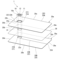
- FIG. 1 is a perspective view of an IC card according to a first embodiment of the present invention, viewed obliquely from the surface side;
- FIG. FIG. 2 is an exploded perspective view of the IC card shown in FIG. 1;
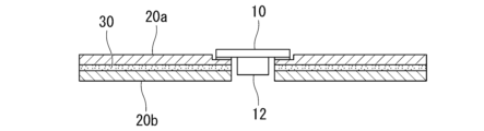
- FIG. 2 is a cross-sectional view taken along the line AA shown in FIG. 1, showing a cross section passing through a slit portion;
- FIG. 2 is a cross-sectional view taken along the line BB shown in FIG. 1, showing a cross section passing through the through-hole portion;
- 2 is an equivalent circuit diagram of the IC card of the first embodiment;
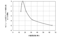
- FIG. FIG. 4 is a diagram showing the relationship between resonance frequency and inter-slit capacitance;
- FIG. 4 is a diagram showing the relationship between the resonance frequency and the module-equipped antenna gain;
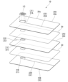
- FIG. 4 is a diagram showing the relationship between the resonance frequency and the imaginary part impedance of the module coil; It is the perspective view which looked at the IC card by 2nd Embodiment from the diagonal surface side.
- FIG. 9 is an exploded perspective view of the IC card shown in FIG. 8;
- FIG. 11 is a perspective view of the IC card according to the third embodiment, viewed obliquely from the surface side;
- FIG. 11 is a perspective view of an IC card according to a fourth embodiment, viewed obliquely from the surface side;
- FIG. 12 is an exploded perspective view of the IC card shown in FIG. 11;
- FIG. 12 is a cross-sectional view taken along line CC shown in FIG. 11, showing a cross section passing through the slit portion;
- FIG. 12 is a cross-sectional view taken along line DD shown in FIG. 11, showing a cross-section passing through the through-hole portion;
- FIG. 11 is an equivalent circuit diagram of an IC card according to a fourth embodiment;
- FIG. 12 is a perspective view of the IC card according to the fifth embodiment, viewed obliquely from the surface side;
- 17 is an exploded perspective view of the IC card shown in FIG. 16;
- FIG. 18 is an exploded perspective view of the middle metal plate of FIG. 17;
- FIG. FIG. 21 is a perspective view of an IC card according to a sixth embodiment, viewed obliquely from the surface side;
- FIG. 11 is a perspective view of an IC card according to a seventh embodiment of the present invention, viewed obliquely from the front side;
- 21 is an exploded perspective view of the IC card shown in FIG. 20;
- FIG. 21 is a cross-sectional view taken along the line EE shown in FIG. 20, showing a cross section passing through the slit portion;
- FIG. 21 is a cross-sectional view taken along line FF shown in FIG. 20, showing a cross-section passing through the through-hole portion;
- FIG. 14 is an equivalent circuit diagram of an IC card of a seventh embodiment;
- FIG. 4 is a diagram showing the relationship between resonance frequency and inter-slit capacitance;
- FIG. 4 is a diagram showing the relationship between the resonance frequency and the module-equipped antenna gain;
- FIG. 4 is a diagram showing the relationship between the resonance frequency and the imaginary part impedance of the module coil;
- FIG. 21 is a perspective view of an IC card according to an eighth embodiment, viewed obliquely from the surface side; 28 is an exploded perspective view of the IC card shown in FIG. 27;
- FIG. FIG. 21 is a perspective view of an IC card according to a ninth embodiment, viewed obliquely from the surface side;
- FIG. 30 is an exploded perspective view of the IC card shown in FIG. 29;
- 3 is an enlarged view of an IC module;
- FIG. FIG. 20 is a perspective view of the IC card according to the tenth embodiment as seen obliquely from the surface side; 33 is an exploded perspective view of the IC card shown in FIG.
- FIG. 20 is an equivalent circuit diagram of the IC card of the tenth embodiment;
- FIG. 20 is an exploded perspective view of an IC card according to an eleventh embodiment;
- 38 is an exploded perspective view of the middle metal plate of FIG. 37;
- an IC card (non-contact communication medium) 1 accommodates an IC module 10 having a planar coil antenna 11 and an IC chip 12, and an IC module 10. It has a metal plate 20 (coupling frame (CF)) whose 20a (metal plate end) functions as an antenna.
- the IC card 1 will be described below with the surface in which the IC module 10 is accommodated as the main surface and the surface opposite to the main surface as the back surface.
- all the metal plates are collectively denoted by reference numeral 20, the metal plate functioning as an antenna is denoted by reference numeral 20A, and the first metal plate is denoted by reference numeral 20A.
- a second metal plate, which is different from the first metal plate 20A and functions as a parallel plate capacitor to be described later, will be referred to as the second metal plate and denoted by reference numeral 20B.
- the metal plate 20 (20A, 20B) has a through hole 21 that fits or overlaps with the IC module 10 and extends from the through hole 21 toward the outer peripheral edge portion 20a in a plan view viewed from the antenna surface of the IC module 10. and a slit 22 .
- At least two or more (in this embodiment, two layers) metal plates 20 are laminated via an insulating layer 30 made of an adhesive layer, and the periphery of the through hole 21 and at least part of the flat coil antenna 11 of the IC module 10 are laminated. are overlapping or close to each other and functioning as antennas. That is, the contactless communication medium 1 of the present embodiment has the first metal plate 20A, the adhesive layer 11, and the second metal plate 20B laminated in that order.
- the second metal plate 20B laminated adjacent to the first metal plate 20A straddles the slits 22 of the first metal plate 20A in a plan view and functions as two plate capacitors connected in series between the slits 22. Add capacitance.
- the metal plate 20 becomes a coil antenna forming a loop circuit by making one turn along the outer peripheral edge portion 20a.
- the coil antenna of this metal plate 20 and the flat plate coil antenna 11 of the IC module 10 are electromagnetically connected.
- the metal plate 20 has a rectangular shape elongated in one direction in plan view.
- the through-hole 21 provided in the metal plate 20 has a substantially rectangular shape and is located at the center of the metal plate 20 in the width direction and near one end in the length direction.
- the metal plate 20 is made of a conductive metallic material such as stainless steel, titanium alloy, or the like.
- the plate thickness of the metal plate 20 is, for example, 100 ⁇ m to 900 ⁇ m.
- the ends along the long axis direction are long sides 20b and 20c, and the ends along the short axis are short sides 20d and 20e.
- the end of the short side on the side closer to the IC module 10 is referred to as the first short side 20d, and the end located on the side opposite to the first short side 20d in the long axis direction is referred to as the second short side.
- Section 20e describes the following contents.
- the first metal plate 20A is electrically connected to the IC module 10 and functions as an antenna by planarly overlapping at least a portion (connection terminal) of the coil antenna 11 of the IC module 10 around the through hole 21. .
- the through hole 21 has a rectangular shape in plan view.
- the shape of the through hole 21 includes round, square, oval, rectangular, and the like.
- the shape of the through hole 21 is not particularly limited as long as it has an opening area that allows electrical connection with the IC module 10 .
- the through hole 21 is formed by, for example, laser processing, cutting, or punching.
- the first through hole 21A provided in the first metal plate 20A is set to have an outer shape smaller than the outer shape of the IC module 10 so that the outer peripheral edge 10a of the IC module 10 overlaps with it in plan view. That is, at least a portion of the metal surface of the first metal plate 20A surrounding the first through hole 21 in plan view overlaps the planar coil antenna 11 of the IC module 10 via an insulating layer or a gap.
- the second through hole 21B of the second metal plate 20B overlaps the first through hole 21A provided in the first metal plate 20A via the insulating layer 30 in plan view.
- a first slit 22A formed in the first metal plate 20A extends from the through hole 21 to the first short side portion 20d along the longitudinal direction.
- One end 22a of the first slit 22A on the side of the first through hole 21A is connected to a corner portion of the first through hole 21A near the first short side portion 20d, and the other end 22b opens to the outer peripheral edge portion 20a. It is connected to the outer peripheral edge portion 20a in this state.
- the direction in which the first slit 22A extends from the first through hole 21A is different from the direction in which the second slit 22B of another metal plate (here, the second metal plate 20B) extends from the second through hole 21B. in a different direction.
- a slit width of the first slit 22A is set to, for example, about 50 ⁇ m to 0.5 mm.
- a second slit 22B formed in the second metal plate 20B extends from the through hole 21 to the second short side portion 20e along the longitudinal direction.
- a state in which one end 22c of the second slit 22B on the side of the second through hole 21B is connected to a corner near the second short side 20e of the second through hole 21B, and the other end 22d opens to the outer peripheral edge 20a. is connected to the outer peripheral edge portion 20a.
- the extending direction of the second slit 22B from the second through hole 21B is different from the extending direction of the first slit 22A of the first metal plate 20A from the first through hole 21A.
- the slit width of the second slit 22B is set to, for example, about 50 ⁇ m to 0.5 mm.
- the two slits 22 (22A, 22B) of the two metal plates 20 (20A, 20B) adjacent to each other in the stacking direction are arranged so as not to overlap with each other for the most part when viewed in plan view, and are arranged on the same line. ing.
- a straight line (line segment) on which these two slits 22 (22A, 22B) are positioned is denoted by K.
- a straight line (line segment) K formed by the slits 22 (22A, 22B) of the two metal plates 20 (20A, 20B) is arranged at a position that bisects the first metal plate 20A into the same area.
- the insulating layer 30 that constitutes the insulator is preferably set to have a thickness of 50 ⁇ m or less, and is interposed between the first metal plate 20A and the second metal plate 20B.
- the dielectric constant of the insulating layer 30 is 1.5 or more.
- the insulating layer 30 can be formed by stacking and pressing a sheet-shaped insulating sheet having an adhesive function on the first metal plate 20A and the second metal plate 20B.
- the insulating layer 30 can be formed by applying a resin having an adhesive function to the surfaces of the first metal plate 20A and the second metal plate 20B and pressing.
- the insulating layer 30 may be formed by applying a resin having an adhesive function to the first metal plate 20A and the second metal plate 20B by screen printing.
- FIG. 4 is an equivalent circuit diagram for explaining the principle of the contactless communication medium 1 of the first embodiment.
- a high-frequency magnetic field is induced in the planar coil antenna 11 of the IC module 10 by a high-frequency signal (not shown) generated by a transmission/reception circuit of a reader/writer (non-contact type external device) (not shown). This high-frequency magnetic field is radiated into space as magnetic energy.
- the contactless communication medium 1 when the contactless communication medium 1 is positioned in this high-frequency magnetic field, the high-frequency magnetic field causes a current to flow through the parallel resonance circuit formed by the antenna of the first metal plate 20A.
- a signal received by this resonance circuit is transmitted to the IC chip 12 by electromagnetic coupling between the antenna coil and the planar coil antenna 11 of the IC module 10 .
- the absolute value of the imaginary part impedance at the communication frequency of the IC chip 12 of the IC module 10 or the frequency of the continuous wave (13.56 MHz) is the imaginary part impedance of the planar coil antenna 11 of the IC module 10 measured by the module alone. It is set to be greater than the absolute value.
- the absolute value of the imaginary part impedance at the communication frequency of the IC chip 12 of the IC module 10 or the frequency of the continuous wave is It is larger than the absolute value of the imaginary part impedance in the attached state and in the state without the second metal plate 20B.
- metal plates 20 (20A, 20B) are designed to have the same outer shape as the IC card 1. As shown in FIG. That is, the outer shape of the metal plate 20 (20A, 20B) is formed like a card.
- FIG. 5 shows the relationship between the resonance frequency (MHz) and the inter-slit capacitance (nF).
- the effective capacitance that the second metal plate 20B forms between the first slits 22A of the first metal plate 20A is lnF or more and 20 nF or less.
- FIG. 6 shows the relationship between the resonance frequency (MHz) and the relative gain (dB) of the metal plate 20 (first metal plate 20A) provided with the IC module 10.
- FIG. 7 shows the correlation between the resonance frequency (MHz) in the first metal plate 20A and the imaginary part impedance of the module coil (after attachment to the first metal plate 20A).
- the IC card 1 is set so that the resonance frequency of the stacked metal plates 20A and 20B with the IC module 10 removed is greater than 13.56 MHz and less than or equal to 25 MHz. Further, as shown in FIG. 7, the imaginary part impedance of the module coil (after attachment to the first metal plate 20A) increases as the resonance frequency approaches 13.56 MHz from a region higher than 13.56 MHz.
- an IC card (non-contact communication medium) 1 has an IC module 10 having a planar coil antenna and an IC chip 12, and a plurality of metal plates 20 whose outer peripheral edges 20a function as antennas.
- the metal plate 20 has a through hole 21 that fits or overlaps with the IC module 10 in plan view, and a slit 22 that extends from the through hole 21 toward the outer peripheral edge portion 20a. At least two metal plates 20 are laminated with the insulating layer 30 interposed therebetween.
- the metal plate 20 has a first metal plate 20A whose periphery of at least one of the through hole 21 and the slit 22 overlaps or is adjacent to at least a part of the planar coil antenna 11 of the IC module 10 and functions as an antenna.
- the second metal plate 20B is two flat plates that straddle the slits 22A of the first metal plate 20A and are connected in series between the slits 22A of the first metal plate 20A in a plan view viewed from the side of the first metal plate 20A.
- Add capacitance as a capacitor Accordingly, the capacitance can be added by a simple method that does not interfere with the card manufacturing process without processing such as connecting a capacitor element between the slits 22A of the first metal plate 20A.
- the self-resonant frequency of the first metal plate 20A can be lowered, and adjustment can be made to improve communication performance at a desired communication frequency.
- the direction in which the slit 22A of at least one of the stacked metal plates 20 (here, the first metal plate 20A) extends from the through hole 21A is
- the direction in which the slit 22B of the other metal plate 20 (here, the second metal plate 20B) extends from the through hole 21B is different.
- the one metal plate 20A and the other metal plate 20B are arranged so that the slits 22A and 22B do not overlap each other and are positioned on the same line in plan view.
- a straight line formed by the slits 22A and 22B of the one metal plate 20A and the other metal plate 20B is provided at a position that divides the area of the metal plate 20 into two.
- At least a part of the metal surface around the through-hole 21 in plan view of at least one metal plate 20 among the plurality of stacked metal plates 20 serves as the planar coil of the IC module 10 . Overlaps the antenna with an insulator or air gap. Thereby, the metal plate 20 and the IC module 10 are electrically connected, and the communication performance of the non-contact communication medium can be improved.
- the thickness of the insulating layer interposed between the laminated metal plates 20 is 100 ⁇ m or less.
- the capacitance formed between the slits 22 of the metal plates 20 can be set to a size that significantly changes the self-resonant frequency of the laminated metal plates 20. becomes.
- the dielectric constant of the insulating layer 30 is 1.5 or higher.
- the capacitance formed between the slits 22 of the metal plates 20 is set more efficiently so that the magnitude thereof is large enough to significantly change the self-resonant frequency of the laminated metal plates 20. can do.
- the insulating layer 30 when the insulating layer 30 is formed by laminating a sheet-like insulating sheet having an adhesive function on a metal plate and pressing it, it can be easily formed using a general card manufacturing process. It becomes possible to card the laminated metal plates 20 .
- the insulating layer 30 when the insulating layer 30 is formed by applying a resin having an adhesive function to the metal plate 20 and pressing the metal plate 20, it can be easily laminated using a general card manufacturing process. It becomes possible to card the metal plate 20 .
- the resin may be applied to the metal plate 20 by screen printing. According to this configuration, not only can the laminated metal plates 20 be easily formed into a card by using a general card manufacturing process, but also the thickness of the insulating layer 30 can be reduced to about several ⁇ m. , more capacitance can be formed between the slits 22 with a smaller number of laminated metal plates 20 .
- the metal plate 20 is formed to have the same shape as the IC card 1, and the second metal plate 20B functioning as a parallel plate capacitor forms an effective capacitance across the slit 22A of the first metal plate 20A. is lnF or more and 20 nF or less, the capacitance formed between the slits 22A of the first metal plate 20A can significantly change the self-resonant frequency of the stacked metal plates 20.
- the metal plate 20 is formed in the same shape as the IC card 1, and when the resonance frequency of the metal plate 20 stacked with the IC module 10 removed is higher than 13.56 MHz and lower than or equal to 25 MHz, The self-resonant frequency of the laminated metal plate 20 itself can significantly change the complex impedance (communication frequency or CW (13.56 MHz) frequency) of both ends (connection terminals) of the coil antenna 11 of the IC module 10. .
- the absolute value of the imaginary part impedance at the communication frequency of the IC chip 12 of the IC module 10 or the frequency of the continuous wave (13.56 MHz) is calculated as the single module in the planar coil antenna 11 of the IC module 10. It can be made larger than the absolute value of the imaginary part impedance at the time of measurement. Further, in this embodiment, the absolute value of the imaginary impedance at the communication frequency or continuous wave frequency of the IC chip 12 of the IC module 10 is measured by can be made larger than the absolute value of the imaginary part impedance in a state in which the second metal plate 20B that forms the plate capacitance is not present.
- the complex impedance (communication frequency or CW (13.56 MHz) frequency) of both ends (IC connection part) of the coil antenna 11 of the IC module 10 can be a complex conjugate with the complex impedance of the input terminal of IC chip 12 .
- the communication performance of the IC card 1 can be improved.
- an IC card (non-contact communication medium) 1B according to the second embodiment will be described with reference to the drawings.
- at least one metal plate 20 (here, the first metal plate 20A) among the plurality of laminated metal plates 20 is The direction in which the slit 22A extends from the through hole 21A is different from the direction in which the slit 22B of the other metal plate 20 (here, the second metal plate 20B) extends from the through hole 21B.
- the one metal plate 20A and the other metal plate 20B are arranged so that the slits 22A and 22B do not overlap each other in plan view.
- a straight line K (see FIG. 8) formed by the slits 22A and 22B of one metal plate 20A and the other metal plate 20B is provided at a position that bisects the metal plate 20 so that the area ratio is less than 1:4. ing. That is, in FIG. 8, the area ratio between the first region D1 and the second region D2 of the metal plate 20 defined by the straight line K is smaller than 1:4. In other words, the area ratio of the first region D1 to the second region D2 is greater than 0.25 (1/4).
- the second embodiment it is possible to prevent the magnitude of the capacitance formed between the slits 22 of the metal plate 20 from becoming too small. Furthermore, by laminating a plurality of metal plates 20 having slits 22 in different positions and directions, the mechanical strength of the IC card 1B against stress due to torsion and bending can be improved.
- an IC card (non-contact communication medium) 1C includes at least one metal plate 20 (here, a second metal plate 20B) among a plurality of stacked metal plates 20. , at least a portion of the metal surface 20f around the through hole 21B in plan view overlaps the planar coil antenna 11 of the IC module 10 via an insulator or an air gap (here, the insulating layer 30). That is, of the metal plates 20 (20A, 20B) overlapping the planar coil antenna 11, the IC module 10 is fitted in the through hole 21A of one metal plate 20A, and the IC module 10 is fitted around the through hole 21B of the other metal plate 20B. The IC modules 10 overlap.
- the other metal plate 20B and the IC module 10 are electrically connected to improve the communication performance of the non-contact communication medium. Also, it is possible to maximize the magnitude of the capacitance formed between the slits 22 of the metal plate 20 . In addition, by laminating a plurality of metal plates 20 having slits 22 in different positions and directions, the mechanical strength of the IC card 1C against stress due to torsion and bending can be improved. Furthermore, by matching the height of the surface of the metal plate 20A laminated on the metal plate 20B and the height of the contact terminal surface of the IC module 10, the surface of the IC card 1C can be decorated with a metal tone.
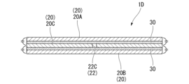
- an IC card (non-contact communication medium) 1D As shown in FIGS. 11 to 14, an IC card (non-contact communication medium) 1D according to the fourth embodiment has three metal plates 20 (20A, 20B, 20C) stacked with insulating layers 30 interposed therebetween. .
- the middle metal plate 20C of the three metal plates 20 (20A, 20B, 20C) is viewed as an antenna, the upper and lower metal plates 20 (20A, 20B) sandwiching the middle metal plate 20C are connected to the middle metal plate 20C.
- a plate series capacitor is loaded that functions as a series connection of two plate capacitors (see FIG. 15).
- the capacitance formed between the slits 22C of the intermediate metal plate 20C can be formed on the front and back sides of the intermediate metal plate 20C, forming a larger capacitance. becomes possible.
- this embodiment by laminating a plurality of metal plates 20 having different positions and directions of the slits 22C, the mechanical strength of the IC card 1D against stress due to torsion and bending can be improved.
- each metal plate 20 functions as an antenna, and the other metal plates 20 (20A, 20B) adjacent to the intermediate metal plate 20C function as flat plate capacitance forming electrodes. .
- the metal plates 20F may be separately formed on both sides of the film substrate 23), the metal foil 24 made of copper or aluminum is formed on one side or both sides 23a and 23b of the resin film substrate 23. It is a thing. That is, the film base material 23 and the metal foil 24 are laminated to each other on the metal plate 20F in which the metal foil 24 is formed on the film base material 23 (see FIG. 18). Thereby, the number of laminated metal plates 20 can be easily increased. Also, the stacked metal plates 20 can be easily carded using a general card manufacturing process.
- an insulating thermoplastic resin is used as the material for forming the film base material 23 .
- the material for forming the film substrate 23 may be a transparent resin or an opaque resin as long as it has insulating properties and thermoplasticity.
- polyester resins such as PEN (polyethylene naphthalate) and PET (polyethylene terephthalate), polycarbonate, polyethylene, polypropylene, polystyrene, and the like can be used.
- the two metal foils 24 independently provided on the front and back surfaces 23a and 23b of the film substrate 23 may be electrically connected by crimping, press-fitting, or welding.
- the two metal foils 24 provided on the front and back sides of the film base 23 are set so that the outer dimensions of the metal foil pattern are smaller than the outer dimensions of the film base 23, and are similar to the outer dimensions of the film base 23 in plan view. are stacked in a state contained inside the
- the inner side of the outer shape of the film substrate 23 means the side on which the film substrate 23 exists.
- the side surface of the film substrate 23 is exposed to the side surface of the IC card 1E. This prevents the adjacent metal foils 24 or the adjacent metal plates 20A and 20B from short-circuiting due to factors such as deformation of the side surface of the IC card 1E, and changes in the communication performance of the stacked metal plates 20.
- the thickness dimension of the metal foil 24 is set to be larger than the skin thickness at the frequency of the continuous wave during communication. This makes it possible to reduce the loss of the current flowing through the metal foil 24 functioning as a part of the metal plate 20 formed on the film substrate 23, and the laminated metal plate 20 including the film substrate 23 can be used. It becomes possible to improve the communication performance of the IC card 1E.
- the through holes 24A of the metal foil patterns of the two metal foils 24 provided on the front and back sides of the film base 23 are set to be larger than the through holes 23A of the film base 23 . That is, in a state where the metal foil 24 is laminated on the film substrate 23, the outer shape of the through hole 23A of the film substrate 23 is included inside the through hole 24A of the metal foil 24 in plan view. Also in this case, only the side surface of the film substrate 23 is exposed to the side surface of the IC card 1E. This prevents the adjacent metal foils 24 or the adjacent metal plates 20A and 20B from short-circuiting due to factors such as deformation of the IC card 1E, and changes in the communication performance of the stacked metal plates 20.
- a through-hole 25 having the same shape as the through-hole 24A or smaller than the through-hole 24A is provided in a portion of the film substrate 23 that corresponds to the through-hole 24A of the metal foil 24 in plan view.
- the metal plates 20A and 20B having the through-holes 21 provided in advance and the metal plate 20F having the metal foil 24 having the through-holes 24A connected to the film substrate 23 can be combined into a common metal plate. It can be easily laminated into a card using card manufacturing processes.
- the above-described film substrate 23 also provides insulation. layer. That is, in the intermediate metal plate 20F, the film substrate 23 between the metal foils 24 becomes an insulating layer.
- the metal foil 24 is made of copper or aluminum, and the thickness dimension of the metal foil 24 is greater than the skin depth at the frequency of the continuous wave during communication. As a result, loss of current flowing through the metal foil 24 functioning as a part of the metal plate 20 formed on the film substrate 23 can be reduced, and the intermediate metal plate 20F composed of the film substrate 23 and the metal foil 24 can be reduced. It is possible to improve the communication performance of the IC card 1E using a plurality of (here, three) metal plates 20 that are stacked.
- an IC card (non-contact communication medium) 1F according to the sixth embodiment is obtained by partially changing the IC card 1E (see FIG. 17, etc.) of the above fifth embodiment. That is, in the intermediate metal plate 20F in the IC card 1F of the sixth embodiment, the size of the through holes 24A in the metal foil pattern of the metal foil 24 is larger than the size of the through holes 23A in the film substrate 23.
- the metal foil 24 is large and is laminated on the film substrate 23 in a state in which it is contained inside the outer shape of the film substrate 23 when viewed from above. That is, the outer shape of the metal foil 24 is smaller than the outer shape of the film substrate 23 .
- the IC card 1F according to the sixth embodiment, only the side surface of the film substrate 23 is exposed to the side surface of the IC card 1F. This makes it possible to prevent the adjacent metal foils 24 or the adjacent metal plates 20 from being short-circuited due to factors such as deformation of the IC card 1F, and the communication performance of the stacked metal plates 20 from changing.
- portions of the film substrate 23 corresponding to the through holes 24A of the metal foil pattern of the metal foil 24 have the same shape as the through holes 24A or are smaller than the through holes 24A.
- a through hole 23A is provided.
- the metal plate 20 provided with the through holes 21 in advance and the film with metal foil having the through holes 24A in the film substrate 23 can be easily laminated using a general card manufacturing process to form a card. becomes possible.
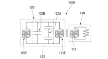
- An IC card (non-contact communication medium) 101 accommodates an IC module 110 having a planar coil antenna 111 and an IC chip 112, and an IC module 110, as shown in FIGS. 20 to 22B. and a metal plate 120 whose 120a (metal plate end) functions as an antenna.
- the metal plate 120 is a coupling frame (CF) that functions as an antenna.
- the IC card 101 will be described below with the surface in which the IC module 110 is accommodated as the main surface and the surface opposite to the main surface as the back surface.
- reference numeral 120 all metal plates are collectively referred to as reference numeral 120, and a metal plate functioning as an antenna as needed is designated as a first metal plate, and reference numeral 120A is attached to the first metal plate.
- a metal plate different from the plate 120A and functioning as a parallel plate capacitor to be described later is defined as a second metal plate, denoted by reference numeral 120B, and will be described below.
- the metal plate 120 has a through hole 121 that fits or overlaps with the IC module 110 in plan view orthogonal to the antenna surface of the IC module 110, and a slit 122 that extends from the through hole 121 toward the outer peripheral edge portion 120a. have.
- the metal plate 120 serves as a coil antenna forming a loop circuit by making one turn along the outer peripheral edge portion 120a.
- the coil antenna of this metal plate 120 and the planar coil antenna 111 of the IC module 110 are electromagnetically connected.
- the metal plate 120 includes a first metal plate 120A functioning as an antenna in which at least one of the perimeter of the through hole 121 and the slit 122 and at least a portion of the planar coil antenna 111 of the IC module 110 overlap or are adjacent to each other. and at least one second metal plate 120B laminated adjacent to the first metal plate 120A. That is, in the IC card 101 of this embodiment, the first metal plate 120A, the insulating layer 130, and the second metal plate 120B are laminated in that order.
- the first metal plate 120A and the second metal plate 120B are physically connected or electrically connected at a low impedance of 30 ⁇ or less at a communication frequency at at least one point (this embodiment Electrically connected), the second metal plate 120B straddles the slits 122 of the first metal plate 120A in plan view and adds capacitance between the slits 122 of the first metal plate 120A.
- the metal plate 120 has a rectangular shape elongated in one direction in plan view.
- the through-hole 121 provided in the metal plate 120 has a substantially rectangular shape and is positioned at the center of the metal plate 120 in the width direction and near one end in the length direction.
- the metal plate 120 is made of, for example, a conductive metallic material such as stainless steel or titanium alloy.
- the plate thickness of the metal plate 120 is, for example, 100 ⁇ m to 900 ⁇ m.
- side portions along the long axis direction are long side portions 120b and 120c
- side portions along the short axis direction are short side portions 120d and 120e.
- the side on the side closer to the IC module 110 is the first short side 120d
- the side opposite to the first short side 120d in the long axis direction is the second short side.
- the following contents will be described as the side portion 120e.
- the first metal plate 120A is electrically connected to the IC module 110 and functions as an antenna by planarly overlapping at least a portion of the planar coil antenna 111 of the IC module 110 around the first through hole 121A.
- the first through hole 121A has a rectangular shape in plan view.
- the shape of the first through hole 121A includes a circle, a square, an oval, an oblong square, and the like.
- the shape of the first through-hole 121A is not particularly limited as long as it has an opening area that allows electrical connection with the IC module 110 .
- 121 A of 1st through-holes are formed by laser processing, cutting, or punching, for example.
- the size of the second through-hole 121B which will be described later, may differ from that of the first through-hole 121A, the shape of the second through-hole 121B is the same as that of the first through-hole 121A. That is, the IC module 110 is fitted into the first through hole 121A.
- the first through hole 121A provided in the first metal plate 120A has an outer shape smaller than the outer shape of the IC module 110 so that the outer peripheral edge 110a of the IC module 110 overlaps in plan view. there is That is, of the first metal plate 120A, at least a portion of the metal surface around the first through hole 121A in plan view overlaps the planar coil antenna 111 of the IC module 110 via an insulating layer or a gap.
- the second through hole 121B of the second metal plate 120B overlaps the first through hole 121A provided in the first metal plate 120A via the insulating layer 130 in plan view.
- a first slit 122A formed in the first metal plate 120A extends along the longitudinal direction from the first through hole 121A to the first short side portion 120d.
- One end 122a of the first slit 122A on the side of the first through hole 121A is connected to one corner 121a of the first through hole 121A near the first short side 120d, and the other end 122b is connected to the outer peripheral edge 120a. It is connected to the outer peripheral edge portion 120a in a state of opening to the outside.
- the direction in which the first through hole 121A of the first slit 122A extends from one corner 121a is the direction in which the second slit 122B of another metal plate (the second metal plate 120B) extends from the second through hole 121B of the second slit 122B described later. different from the exit direction.
- the slit width of the first slit 122A is set to, for example, 50 ⁇ m to 0.5 mm.
- a second slit 122B formed in the second metal plate 120B extends from the through hole 121 to the first short side portion 120d along the longitudinal direction.
- One end 122c of the second slit 122B on the side of the second through hole 121B is connected to the other corner 121b near the first short side 120d of the second through hole 121B, and the other end 122d is connected to the outer peripheral edge 120a. It is connected to the outer peripheral edge portion 120a in a state of opening to the outside.
- the extending direction of the second slit 122B from the second through hole 121B is different from the extending direction from one corner 121a of the first through hole 121A of the first slit 122A of the first metal plate 120A.
- the slit width of the second slit 122B is set to, for example, 50 ⁇ m to 0.5 mm.
- the first metal plate 20A and the second metal plate 20B are arranged so that the slits 22A and 22B in plan view do not overlap with each other for the most part. As shown in FIG. 20, it has a first area K1 partitioned by a first slit 122A, a second slit 122B, and through holes 121A, 121B, and a second area K2 that is not partitioned.
- the first metal plate 120A and the second metal plate 120B are physically connected in either the first region K1 or the second region K2, or have a low impedance of 30 ⁇ or less at the communication frequency. electrically connected.
- the area where the first metal plate 120A and the second metal plate 120B are physically or electrically connected is the smaller area of the first area K1 and the second area K2 in plan view. be.
- the first region K1 since the area of the first region K1 is smaller than the area of the second region K2, the first region K1 serves as the connecting portion.
- the area ratio between the first area K1 and the second area K2 is at least greater than 1:4. In other words, the area ratio of the first region K1 to the second region K2 is preferably at least less than 0.25 (1/4).
- the insulating layer 130 that constitutes the insulator is preferably set to have a thickness of 100 ⁇ m or less, and is interposed between the first metal plate 120A and the second metal plate 120B.
- the dielectric constant of the insulating layer 130 is 1.5 or more.
- the insulating layer 130 can be formed by pressing a sheet-shaped insulating sheet having an adhesive function while being laminated on the first metal plate 120A and the second metal plate 120B.
- the insulating layer 130 can be formed by applying a resin having an adhesive function to the surfaces of the first metal plate 120A and the second metal plate 120B and pressing them.
- the insulating layer 130 may be formed by applying the resin to the first metal plate 120A and the second metal plate 120B by screen printing.
- a part of the insulating layer 130 is made of a member having conductivity (the conductive member 140).
- the conductive member 140 is a conductive resin, an anisotropic conductive resin, metal flakes, solder, a resin ball having a metal layer formed on its surface, or a spring having a metal layer formed on its surface.
- the conductive member 140 is a part where the first metal plate 120A and the second metal plate 120B are electrically connected with a low impedance of 30 ⁇ or less at the communication frequency.
- the first metal plate 120A and the second metal plate 120B are electrically or physically connected via a conductive member 140 provided by a connection method such as application of a conductive material, welding, plating, pressure contact, screwing, soldering, or the like. properly connected.
- FIG. 23 is an equivalent circuit diagram for explaining the principle of the IC card 101 of the seventh embodiment.
- a high-frequency magnetic field is induced in the planar coil antenna 111 of the IC module 110 by a high-frequency signal (not shown) generated by a transmitting/receiving circuit of a reader/writer (non-contact type external device) (not shown). This high-frequency magnetic field is radiated into space as magnetic energy.
- the high-frequency magnetic field causes a current to flow through the parallel resonance circuit formed by the antenna of the first metal plate 120A.
- a signal received by this resonance circuit is transmitted to the IC chip 112 by electromagnetic coupling between the antenna coil and the planar coil antenna 111 of the IC module 110 .
- the absolute value of the imaginary part impedance at the communication frequency of the IC chip 12 of the IC module 110 or the frequency of the continuous wave (13.56 MHz) is the imaginary part impedance of the planar coil antenna 111 of the IC module 110 measured by the module alone. It is set to be greater than the absolute value.
- the absolute value of the imaginary part impedance at the communication frequency of the IC chip 112 of the IC module 110 or the frequency of the continuous wave is It is larger than the absolute value of the imaginary part impedance in the attached state and in the state without the second metal plate 120B.
- the IC card 101 of this embodiment is set such that the metal plates 120 (120A, 120B) have the same shape as the IC card 101.
- the outer shape of the metal plate 120 (120A, 120B) is formed like a card.
- FIG. 24 shows the relationship between the resonance frequency (MHz) and the inter-slit capacitance (nF).
- the effective capacitance formed by the second metal plate 120B across the first slits 122A of the first metal plate 120A is lnF or more and 20 nF or less.
- FIG. 25 shows the relationship between the resonance frequency (MHz) and the relative gain (dB) of the metal plate 120 (first metal plate 120A) provided with the IC module 110.
- FIG. FIG. 26 shows the correlation between the resonance frequency (MHz) in the first metal plate 120A and the imaginary part impedance of the module coil (after attachment to the first metal plate 120A).
- the IC card 101 is set so that the resonance frequency of the stacked metal plates 120A and 120B with the IC module 110 removed is greater than 13.56 MHz and less than or equal to 25 MHz. Also, as shown in FIG. 26, the imaginary impedance of the module coil (after attachment to the first metal plate 120A) increases as the resonance frequency approaches 13.56 MHz from a region higher than 13.56 MHz.
- the complex impedance (communication frequency or CW (13.56 MHz) frequency) at both ends (IC connection part) of the planar coil antenna 111 of the IC module 110 is It can be a complex conjugate with the complex impedance of the input terminal. This makes it possible to improve the communication performance of the IC card 101 .
- the first metal plate 120A functioning as an antenna and at least one second metal plate 120B laminated adjacent to the first metal plate 120A are physically connected at at least one point
- the second metal plate 120B is electrically connected with a low impedance of 30 ⁇ or less at the communication frequency, and the second metal plate 120B straddles the slits 122 of the first metal plate 120A in plan view and adds capacitance between the slits 122. do.
- the capacitance can be added by a simple method that does not interfere with the card manufacturing process without processing such as connecting a capacitor element between the slits 122 of the first metal plate 120A that functions as an antenna. .
- the capacitance between the slits 122 it is possible to lower the self-resonant frequency of the metal plate 120, and it is possible to adjust so as to improve communication performance at a desired communication frequency.
- the direction in which the slit 122 of at least one of the stacked metal plates 120 extends from the through hole 121 is the same as the direction in which the slits 122 of the other metal plates 120 extend. are different positions, and are arranged so that the slits 122 of two metal plates 120 adjacent in the stacking direction do not overlap each other in a plan view.
- the first metal plate 120A and the second metal plate 120B are physically connected or electrically connected with a low impedance of 30 ⁇ or less at the communication frequency.
- the first metal plate 120A and the second metal plate 120B are physically connected or communicated in the smaller area of the first area K1 and the second area K2 in plan view. They are electrically connected with a low impedance of 30 ⁇ or less at the frequency. This makes it possible to maximize the magnitude of the capacitance formed between the slits 122 of the metal plate 120 . Moreover, by laminating a plurality of metal plates 120 having slits 122 in different positions and directions, the mechanical strength of the IC card 101 against stress due to torsion and bending can be improved.
- the area ratio of the first area K1 and the second area K2 is at least greater than 1:4. In other words, the area ratio of the first region K1 to the second region K2 is at least less than 0.25 (1/4). This makes it possible to maximize the magnitude of the capacitance formed between the slits 122 of the metal plate 120 . Moreover, by laminating a plurality of metal plates 120 having slits 122 in different positions and directions, the mechanical strength of the IC card 101 against stress due to torsion and bending can be improved.
- the IC module 110 is provided in the through hole 121 of one of the stacked metal plates 120, and the planar coil antenna 111 of the IC module 110 has a Then, at least a portion of the peripheral portion of the through hole 121 overlaps, and at least a portion of the planar coil antenna 111 of the IC module 110 overlaps with the through hole 121 of the other metal plate 120 in plan view. Thereby, the metal plate 120 and the IC module 110 are electrically connected, and the communication performance of the IC card 101 can be improved. Also, by matching the height of the surface of the metal plate 120 laminated on the metal plate 120 and the height of the contact terminal surface of the IC module 110, the surface of the IC card 101 can be decorated with a metallic tone.
- the thickness of the insulating layer 130 interposed between the first metal plate 120A and the second metal plate 120B is 100 ⁇ m or less, and preferably the dielectric constant of the insulating layer 130 is 1.5. That's it.
- the capacitance formed between the slits 122 of the metal plates 120 can be set to a size that significantly changes the self-resonant frequency of the stacked metal plates 120. becomes.
- the insulating layer 130 is formed by laminating a sheet-shaped insulating sheet having an adhesive function on the metal plate and pressing. This makes it possible to easily form the stacked metal plates 120 into a card using a general card manufacturing process.
- the insulating layer 130 is formed by applying a resin having an adhesive function to the metal plate 120 and pressing. This makes it possible to easily form the stacked metal plates 120 into a card using a general card manufacturing process.
- the insulating layer 130 is formed by applying the resin to the metal plate 120 by screen printing. This makes it possible to easily form the stacked metal plates 120 into a card using a general card manufacturing process. Furthermore, the thickness of the insulating layer 130 can be set to about several ⁇ m. As a result, a larger amount of capacitance can be formed between the slits 122 with a smaller number of laminated metal plates 120 .
- the insulating layer 130 between the laminated metal plates 120 is made of the conductive member 140 .
- the electrostatic capacitance between the slits 122 of the metal plate 120 on the side that functions as an antenna is eliminated without conduction. It becomes possible to make it larger than the case, and it becomes easy to significantly change the self-resonant frequency of the laminated metal plates 120 .
- the conductive member 140 is made of a conductive resin, an anisotropic conductive resin, metal flakes, solder, a resin ball having a metal layer formed on its surface, or a spring having a metal layer formed on its surface. is.
- the metal plate 120 has the same shape as the IC card 101, and the second metal plate 120 (120B) is formed between the slits 122 of the first metal plate 120 (120A). Effective capacitance is greater than or equal to lnF and less than or equal to 20nF. Thereby, the capacitance formed between the slits 122 of the metal plates 120 can significantly change the self-resonant frequency of the stacked metal plates 120 .
- the first metal plate 120 can be provided with a through hole instead of the conductive member 140 described above. are electrically or physically connected by applying a conductive material, welding, plating, crimping, screwing, soldering, or the like. As a result, it is possible to expand the range of utilization of the technique of electrically connecting a part of the laminated metal plates 120 with low impedance at the communication frequency. Furthermore, since the connection portion (through hole) is covered with the module when viewed from the surface of the IC card 101, the external appearance of the IC card 101 is not spoiled.
- the outer shape of the metal plate 120 is the same as that of the IC card 101, and when the IC module 110 is removed, the resonance frequency of the stacked metal plates 120 is higher than 13.56 MHz. 25 MHz or less.
- the self-resonant frequency of the laminated metal plates 120 themselves changes to the complex impedance (communication frequency or CW (13.56 MHz) frequency ) can be significantly changed.
- an IC module 110 is provided in a through hole 121 of one metal plate 120A of stacked metal plates 120A and 120B. At least part of the peripheral portion 121c of the through hole 121 in the other metal plate 120B overlaps the planar coil antenna 111 of the IC module 110 with the insulating layer 130 interposed therebetween. Note that at least a portion of the peripheral portion 121c of the through hole 121 in the other metal plate 120B is not limited to overlapping the planar coil antenna 111 of the IC module 110 with the insulation of the insulating layer 130 interposed therebetween. may overlap the planar coil antenna 111 of the IC module 110 .
- a conductive member 140 is provided in a portion of the insulating layer 130 between the laminated metal plates 120A and 120B, as in the seventh embodiment described above.
- a through-hole 121A of one metal plate 120A has the same dimensions as the IC module 110 or a dimension larger than the IC module 110, and is set so that the IC module 110 can be fitted in a plan view.
- the through hole 121B of the other metal plate 120B is set to be smaller than the outer shape of the IC module 110, as in the seventh embodiment described above.
- the metal plate 120 and the IC module 110 are electrically connected, and the communication performance of the IC card 101B can be improved.
- the surface of the first metal plate 120A laminated on the second metal plate 120B is aligned with the height of the contact terminal surface of the IC module 110, so that the surface of the IC card 101B is decorated with a metal tone. It is also possible to
- the first metal plate 120A and the second metal plate 120B are electrically connected with a low impedance of 30 ⁇ or less at the communication frequency.
- Through hole 141 is provided in a region where first metal plate 120A and planar coil antenna 111 of IC module 110 overlap. This conductive through-hole 141 penetrates not only the first metal plate 120A but also the insulating layer 130 .
- the conductive through-hole 141 of the ninth embodiment has a diameter dimension smaller than that of the conductive member 140 of the above-described seventh and eighth embodiments. Through this conductive through-hole 141, the first metal plate 120A and the second metal plate 120B are electrically connected.
- the conductive through-holes 141 serving as the connecting portions are covered with the IC module 110 in a plan view seen from the surface of the IC card 101C. This can prevent the appearance of the IC card 101C from being spoiled.
- the intermediate metal plate 120E overlaps the planar coil antenna 111 via an insulator or a gap (corresponding to the insulating layer 130 in this embodiment) in at least a portion of the peripheral portion 120f (see FIG. 35) of the through hole 121E. ing.
- One metal plate 120A functions as a plate series capacitor in which two plate capacitors are connected in series between the slits 122E of the middle metal plate 120E.
- the other metal plate 120B is partially physically connected to the intermediate metal plate 120E, or electrically connected so as to have a low impedance of 30 ⁇ or less at the communication frequency. , between the slits 122E, it functions to form a plate capacitance.
- the capacitance formed between the slits 122E of the intermediate metal plate 120E can be formed on the front and back sides of the metal plate 120E, resulting in a larger static capacitance. It becomes possible to form a capacitance. Furthermore, by stacking the metal plates 120A and 120B above and below the intermediate metal plate 120E, each of the metal plates 120A and 120B functions as an antenna, and the metal plates 120A and 120B adjacent to the intermediate metal plate 120E are flat plates. It functions as a capacitance forming electrode. This makes it possible to adjust the self-resonant frequency of the stacked metal plates 120 to a lower level.
- the IC card 101E according to the eleventh embodiment shown in FIGS.
- the metal plate 120 of (which may be formed separately) is formed by forming a metal foil 124 made of copper or aluminum on one side or both sides 123a, 123b of a resin film substrate 123.
- the metal plate 120 ⁇ /b>F in which the metal foil 124 is formed on the film base 123 the film base 123 and the metal foil 124 are laminated with the insulating layer 130 interposed therebetween. Therefore, when the film substrate 123 has the metal foils 124 on both sides, there are substantially four metal layers (see FIG. 37). Thereby, the number of laminated metal plates 120 can be easily increased. Also, the stacked metal plates 120 can be easily carded using a general card manufacturing process.
- the material forming the film substrate 123 is, for example, an insulating thermoplastic resin.
- the material forming the film substrate 123 may be a transparent resin or an opaque resin as long as it has insulating properties and thermoplasticity.
- polyester resins such as PEN (polyethylene naphthalate) and PET (polyethylene terephthalate), polycarbonate, polyethylene, polypropylene, polystyrene, and the like can be used.
- the metal foils 124 provided on the front and back surfaces 123a and 123b of the film base 123 may be electrically connected by crimping, pressure contact, or welding.
- the two metal foils 124 provided on the front and back surfaces 123a and 123b of the film base 123 are set so that the outer dimensions of the metal foil pattern are smaller than the outer dimensions of the film base 123, and are the same as the film base when viewed from above.
- 123 are stacked while being contained inside the outer shape of 123 .
- the inner side of the outer shape of the film substrate 123 means the side where the film substrate 123 exists.
- only the side surface of the film substrate 123 is exposed to the side surface of the IC card 101E. This prevents the adjacent metal foils 124 or the adjacent metal plates 120A and 120B from short-circuiting due to factors such as deformation of the IC card 101E, and changes in the communication performance of the stacked metal plates 120.
- the thickness dimension of the metal foil 124 is set to be larger than the skin thickness at the frequency of the continuous wave during communication. As a result, loss of current flowing through the metal foil 124 functioning as a part of the metal plate 120 formed on the film substrate 123 can be reduced, and the laminated metal plate 120 including the film substrate 123 can be used. It is possible to improve the communication performance of the IC card 101E.
- the through holes 124A of the metal foil pattern in the metal foil 124 are set to be larger in size than the through holes 123A of the film substrate 123.
- the outer shape of the through hole 123A of the film substrate 123 is included inside the through hole 124A of the metal foil 124 in plan view.
- only the side surface of the film substrate 123 is exposed to the side surface (through hole side) of the IC card 101E. This prevents the adjacent metal foils 124 or the adjacent metal plates 120A and 120B from short-circuiting due to factors such as deformation of the IC card 101E, and changes in the communication performance of the stacked metal plates 120.
- the planar coil antenna 111 of the IC module 110 accommodated in the through hole 121A of the metal plate 120A is directly connected to the intermediate metal plate via the insulating layer 130. It is arranged on the through hole 121F of 120F.
- a material such as aluminum or copper can be used rather than a metal plate, which is often made of SUS metal. More current flows through the metal foil 124 on the film substrate 123 with high electrical conductivity used. This makes it possible to improve the communication performance of the IC card 101E using a plurality of (here, three) laminated metal plates 120 including the intermediate metal plate 120F composed of the film substrate 123 and the metal foil 124. .
- the film substrate 123 described above is also used. It becomes an insulating layer. That is, in the intermediate metal plate 120F, the film substrate 123 between the metal foils 124 becomes an insulating layer.
- a crimped portion 125 is formed between the slits 122F of the intermediate metal plate 120F.
- the crimped portion 125 is crimped, for example, so as to protrude toward the upper side or the lower side of the surface of the IC card 101E, that is, toward the metal plate 120A or 120B.
- the metal plates 120A and 120B overlapping the crimped portion 125 of the intermediate metal plate 120F have recesses to avoid the crimped portion 125.
- the recessed portion 126 forms a physical unevenness that electrically connects the metal patterns on the front and back sides of the metal plates 120A and 120B stacked above and below the metal plate 120F including the film substrate 123.
- This recessed portion 126 can prevent a change in the electrical performance of the antenna due to contact with other metal plates 10 when a plurality of metal plates 120 are laminated to form the IC card 101E.
- the recessed portion 126 may be a through hole.
- the capacitance can be increased with a simple structure.
- IC card (non-contact communication medium) REFERENCE SIGNS LIST 10 IC module 11 planar coil antenna 12 IC chip 20 metal plate 20a outer peripheral edge (metal plate end) 20A first metal plate 20B second metal plate 20C intermediate metal plate 21 through hole 22 slit 23 film substrate 24 metal foil 25 through hole 30 insulating layer 101, 101B to 101E IC card (non-contact communication medium) 110 IC module 111 planar coil antenna 112 IC chip 120 metal plate 120A first metal plate 120B second metal plate 121 through hole 122 slit 125 caulked portion 126 recessed portion 130 insulating layer 140 conductive member 141 conductive through hole
Landscapes
- Engineering & Computer Science (AREA)
- Microelectronics & Electronic Packaging (AREA)
- Computer Hardware Design (AREA)
- Physics & Mathematics (AREA)
- General Physics & Mathematics (AREA)
- Theoretical Computer Science (AREA)
- Computer Networks & Wireless Communication (AREA)
- Credit Cards Or The Like (AREA)
Priority Applications (4)
| Application Number | Priority Date | Filing Date | Title |
|---|---|---|---|
| EP22918903.0A EP4462598A4 (en) | 2022-01-07 | 2022-12-28 | CONTACTLESS COMMUNICATION MEDIUM |
| CN202280086098.XA CN118451607A (zh) | 2022-01-07 | 2022-12-28 | 非接触通信介质 |
| JP2023572467A JPWO2023132320A1 (https=) | 2022-01-07 | 2022-12-28 | |
| US18/765,187 US12333368B2 (en) | 2022-01-07 | 2024-07-05 | Contactless communication medium |
Applications Claiming Priority (4)
| Application Number | Priority Date | Filing Date | Title |
|---|---|---|---|
| JP2022001774 | 2022-01-07 | ||
| JP2022-001774 | 2022-01-07 | ||
| JP2022001769 | 2022-01-07 | ||
| JP2022-001769 | 2022-01-07 |
Related Child Applications (1)
| Application Number | Title | Priority Date | Filing Date |
|---|---|---|---|
| US18/765,187 Continuation US12333368B2 (en) | 2022-01-07 | 2024-07-05 | Contactless communication medium |
Publications (1)
| Publication Number | Publication Date |
|---|---|
| WO2023132320A1 true WO2023132320A1 (ja) | 2023-07-13 |
Family
ID=87073693
Family Applications (1)
| Application Number | Title | Priority Date | Filing Date |
|---|---|---|---|
| PCT/JP2022/048556 Ceased WO2023132320A1 (ja) | 2022-01-07 | 2022-12-28 | 非接触通信媒体 |
Country Status (4)
| Country | Link |
|---|---|
| US (1) | US12333368B2 (https=) |
| EP (1) | EP4462598A4 (https=) |
| JP (1) | JPWO2023132320A1 (https=) |
| WO (1) | WO2023132320A1 (https=) |
Families Citing this family (2)
| Publication number | Priority date | Publication date | Assignee | Title |
|---|---|---|---|---|
| DE102021005960A1 (de) * | 2021-12-02 | 2023-06-07 | Giesecke+Devrient Mobile Security Gmbh | Kartenförmiger Datenträger mit einer Hinterspritzungsschicht und Verfahren zum Herstellen eines kartenförmigen Datenträgers |
| JPWO2023132320A1 (https=) * | 2022-01-07 | 2023-07-13 |
Citations (4)
| Publication number | Priority date | Publication date | Assignee | Title |
|---|---|---|---|---|
| JP2014075775A (ja) * | 2012-05-21 | 2014-04-24 | Murata Mfg Co Ltd | アンテナ装置および無線通信装置 |
| US20180123221A1 (en) * | 2014-08-10 | 2018-05-03 | David Finn | Smartcards, rfid devices, wearables and methods |
| JP2022001774A (ja) | 2020-06-19 | 2022-01-06 | 古河電気工業株式会社 | 被装着部材の固定構造、装着部品、及び、装着部品の固定方法 |
| JP2022001769A (ja) | 2020-06-19 | 2022-01-06 | 川崎重工業株式会社 | 液圧駆動システム |
Family Cites Families (12)
| Publication number | Priority date | Publication date | Assignee | Title |
|---|---|---|---|---|
| US20090145971A1 (en) * | 2007-12-07 | 2009-06-11 | Wen Cheng Yin | Printed wireless rf identification label structure |
| MX2010008213A (es) * | 2008-02-22 | 2010-09-30 | Toppan Printing Co Ltd | Transpondedor y cuaderno. |
| EP2889811B1 (en) * | 2009-04-28 | 2020-04-15 | Toppan Printing Co., Ltd. | Antenna sheet, data carrier with non-contact IC, and method for manufacturing antenna sheet |
| US9275322B2 (en) * | 2013-11-25 | 2016-03-01 | VivaLnk Limited (Cayman Islands) | Stretchable multi-layer wearable tag capable of wireless communications |
| KR101754985B1 (ko) * | 2016-04-21 | 2017-07-19 | 주식회사 아이씨케이 | 비접촉식 카드 기능을 갖는 메탈 카드 및 그 제조 방법 |
| KR102798748B1 (ko) | 2017-02-15 | 2025-04-22 | 에스케이하이닉스 주식회사 | 하이브리드 메모리 시스템 및 그 제어 방법 |
| JP6597921B2 (ja) * | 2017-10-20 | 2019-10-30 | 株式会社村田製作所 | カード型無線通信デバイス |
| US12277462B2 (en) * | 2019-08-14 | 2025-04-15 | Federal Card Services, LLC | Metal-containing dual interface smartcards |
| US20240249104A1 (en) * | 2021-06-14 | 2024-07-25 | Metaland Llc | Rfid enabled metal transaction cards |
| US12159180B1 (en) * | 2021-11-29 | 2024-12-03 | Metaland Llc | RFID enabled metal transaction cards with coupler coil couplings and related methods |
| DE102021005960A1 (de) * | 2021-12-02 | 2023-06-07 | Giesecke+Devrient Mobile Security Gmbh | Kartenförmiger Datenträger mit einer Hinterspritzungsschicht und Verfahren zum Herstellen eines kartenförmigen Datenträgers |
| JPWO2023132320A1 (https=) * | 2022-01-07 | 2023-07-13 |
-
2022
- 2022-12-28 JP JP2023572467A patent/JPWO2023132320A1/ja active Pending
- 2022-12-28 WO PCT/JP2022/048556 patent/WO2023132320A1/ja not_active Ceased
- 2022-12-28 EP EP22918903.0A patent/EP4462598A4/en active Pending
-
2024
- 2024-07-05 US US18/765,187 patent/US12333368B2/en active Active
Patent Citations (4)
| Publication number | Priority date | Publication date | Assignee | Title |
|---|---|---|---|---|
| JP2014075775A (ja) * | 2012-05-21 | 2014-04-24 | Murata Mfg Co Ltd | アンテナ装置および無線通信装置 |
| US20180123221A1 (en) * | 2014-08-10 | 2018-05-03 | David Finn | Smartcards, rfid devices, wearables and methods |
| JP2022001774A (ja) | 2020-06-19 | 2022-01-06 | 古河電気工業株式会社 | 被装着部材の固定構造、装着部品、及び、装着部品の固定方法 |
| JP2022001769A (ja) | 2020-06-19 | 2022-01-06 | 川崎重工業株式会社 | 液圧駆動システム |
Non-Patent Citations (1)
| Title |
|---|
| See also references of EP4462598A4 |
Also Published As
| Publication number | Publication date |
|---|---|
| EP4462598A1 (en) | 2024-11-13 |
| JPWO2023132320A1 (https=) | 2023-07-13 |
| US12333368B2 (en) | 2025-06-17 |
| EP4462598A4 (en) | 2025-04-09 |
| US20240362450A1 (en) | 2024-10-31 |
Similar Documents
| Publication | Publication Date | Title |
|---|---|---|
| US7775446B2 (en) | Card type information device and method for manufacturing same | |
| US8544759B2 (en) | Wireless IC device, wireless IC module and method of manufacturing wireless IC module | |
| US8847844B2 (en) | Antenna and antenna module | |
| US7408512B1 (en) | Antenna with distributed strip and integrated electronic components | |
| US7990326B2 (en) | Antenna apparatus and adjusting method thereof | |
| EP1073009B1 (en) | IC card | |
| US10396429B2 (en) | Wireless communication device | |
| CN106030618B (zh) | 无线通信装置及其制造方法、以及带rfic元件贴片及其制作方法 | |
| US12333368B2 (en) | Contactless communication medium | |
| EP1814191A2 (en) | Antenna apparatus | |
| JP4605318B2 (ja) | アンテナ及び無線icデバイス | |
| EP0790665A1 (en) | Chip antenna | |
| KR20080064863A (ko) | 안테나 내장 모듈과 카드형 정보 장치 및 그들의 제조 방법 | |
| US20030016506A1 (en) | Non-contact type IC card and flat coil used for the same | |
| US10122065B2 (en) | Antenna device, card information medium, electronic apparatus, and method for manufacturing antenna device | |
| JPWO2023132320A5 (https=) | ||
| JP5187083B2 (ja) | Rfidタグ、rfidシステム及びrfidタグ製造方法 | |
| JP2012094948A (ja) | 非接触通信記録媒体用インレット及びその製造方法及び非接触通信記録媒体 | |
| JP3421334B2 (ja) | Icタグ | |
| JP2019128706A (ja) | Rfidタグ | |
| JP6048740B2 (ja) | 非接触式icカード用又は非接触式icタグ用の回路基板及び非接触式icカード又は非接触式icタグ | |
| CN219418172U (zh) | 抗金属电子标签 | |
| JPH0415990A (ja) | 高周波回路モジュールの接続方法 | |
| CN118451607A (zh) | 非接触通信介质 | |
| JP2002049902A (ja) | Icタグ |
Legal Events
| Date | Code | Title | Description |
|---|---|---|---|
| 121 | Ep: the epo has been informed by wipo that ep was designated in this application |
Ref document number: 22918903 Country of ref document: EP Kind code of ref document: A1 |
|
| WWE | Wipo information: entry into national phase |
Ref document number: 202280086098.X Country of ref document: CN |
|
| ENP | Entry into the national phase |
Ref document number: 2023572467 Country of ref document: JP Kind code of ref document: A |
|
| WWE | Wipo information: entry into national phase |
Ref document number: 2022918903 Country of ref document: EP |
|
| NENP | Non-entry into the national phase |
Ref country code: DE |
|
| ENP | Entry into the national phase |
Ref document number: 2022918903 Country of ref document: EP Effective date: 20240807 |