WO2023120574A1 - エナジーハーベスタ、及び充電装置 - Google Patents
エナジーハーベスタ、及び充電装置 Download PDFInfo
- Publication number
- WO2023120574A1 WO2023120574A1 PCT/JP2022/047109 JP2022047109W WO2023120574A1 WO 2023120574 A1 WO2023120574 A1 WO 2023120574A1 JP 2022047109 W JP2022047109 W JP 2022047109W WO 2023120574 A1 WO2023120574 A1 WO 2023120574A1
- Authority
- WO
- WIPO (PCT)
- Prior art keywords
- coil
- section
- energy harvester
- circuit
- antenna
- Prior art date
- Legal status (The legal status is an assumption and is not a legal conclusion. Google has not performed a legal analysis and makes no representation as to the accuracy of the status listed.)
- Ceased
Links
Images


Classifications
-
- H—ELECTRICITY
- H02—GENERATION; CONVERSION OR DISTRIBUTION OF ELECTRIC POWER
- H02J—ELECTRIC POWER NETWORKS; CIRCUIT ARRANGEMENTS OR SYSTEMS FOR SUPPLYING OR DISTRIBUTING ELECTRIC POWER; SYSTEMS FOR STORING ELECTRIC ENERGY
- H02J50/00—Circuit arrangements or systems for wireless supply or distribution of electric power
- H02J50/10—Circuit arrangements or systems for wireless supply or distribution of electric power using inductive coupling
- H02J50/12—Circuit arrangements or systems for wireless supply or distribution of electric power using inductive coupling of the resonant type
-
- H—ELECTRICITY
- H01—ELECTRIC ELEMENTS
- H01M—PROCESSES OR MEANS, e.g. BATTERIES, FOR THE DIRECT CONVERSION OF CHEMICAL ENERGY INTO ELECTRICAL ENERGY
- H01M10/00—Secondary cells; Manufacture thereof
- H01M10/42—Methods or arrangements for servicing or maintenance of secondary cells or secondary half-cells
- H01M10/44—Methods for charging or discharging
-
- H—ELECTRICITY
- H01—ELECTRIC ELEMENTS
- H01M—PROCESSES OR MEANS, e.g. BATTERIES, FOR THE DIRECT CONVERSION OF CHEMICAL ENERGY INTO ELECTRICAL ENERGY
- H01M10/00—Secondary cells; Manufacture thereof
- H01M10/42—Methods or arrangements for servicing or maintenance of secondary cells or secondary half-cells
- H01M10/46—Accumulators structurally combined with charging apparatus
-
- H—ELECTRICITY
- H02—GENERATION; CONVERSION OR DISTRIBUTION OF ELECTRIC POWER
- H02J—ELECTRIC POWER NETWORKS; CIRCUIT ARRANGEMENTS OR SYSTEMS FOR SUPPLYING OR DISTRIBUTING ELECTRIC POWER; SYSTEMS FOR STORING ELECTRIC ENERGY
- H02J50/00—Circuit arrangements or systems for wireless supply or distribution of electric power
- H02J50/001—Energy harvesting or scavenging
-
- H—ELECTRICITY
- H02—GENERATION; CONVERSION OR DISTRIBUTION OF ELECTRIC POWER
- H02J—ELECTRIC POWER NETWORKS; CIRCUIT ARRANGEMENTS OR SYSTEMS FOR SUPPLYING OR DISTRIBUTING ELECTRIC POWER; SYSTEMS FOR STORING ELECTRIC ENERGY
- H02J50/00—Circuit arrangements or systems for wireless supply or distribution of electric power
- H02J50/005—Mechanical details of housing or structure aiming to accommodate the power transfer means, e.g. mechanical integration of coils, antennas or transducers into emitting or receiving devices
-
- H—ELECTRICITY
- H02—GENERATION; CONVERSION OR DISTRIBUTION OF ELECTRIC POWER
- H02J—ELECTRIC POWER NETWORKS; CIRCUIT ARRANGEMENTS OR SYSTEMS FOR SUPPLYING OR DISTRIBUTING ELECTRIC POWER; SYSTEMS FOR STORING ELECTRIC ENERGY
- H02J50/00—Circuit arrangements or systems for wireless supply or distribution of electric power
- H02J50/10—Circuit arrangements or systems for wireless supply or distribution of electric power using inductive coupling
-
- H—ELECTRICITY
- H02—GENERATION; CONVERSION OR DISTRIBUTION OF ELECTRIC POWER
- H02J—ELECTRIC POWER NETWORKS; CIRCUIT ARRANGEMENTS OR SYSTEMS FOR SUPPLYING OR DISTRIBUTING ELECTRIC POWER; SYSTEMS FOR STORING ELECTRIC ENERGY
- H02J50/00—Circuit arrangements or systems for wireless supply or distribution of electric power
- H02J50/20—Circuit arrangements or systems for wireless supply or distribution of electric power using microwaves or radio frequency waves
- H02J50/27—Circuit arrangements or systems for wireless supply or distribution of electric power using microwaves or radio frequency waves characterised by the type of receiving antennas, e.g. rectennas
-
- H—ELECTRICITY
- H02—GENERATION; CONVERSION OR DISTRIBUTION OF ELECTRIC POWER
- H02J—ELECTRIC POWER NETWORKS; CIRCUIT ARRANGEMENTS OR SYSTEMS FOR SUPPLYING OR DISTRIBUTING ELECTRIC POWER; SYSTEMS FOR STORING ELECTRIC ENERGY
- H02J50/00—Circuit arrangements or systems for wireless supply or distribution of electric power
- H02J50/40—Circuit arrangements or systems for wireless supply or distribution of electric power using two or more transmitting or receiving devices
- H02J50/402—Circuit arrangements or systems for wireless supply or distribution of electric power using two or more transmitting or receiving devices the two or more transmitting or the two or more receiving devices being integrated in the same unit, e.g. power mats with several coils or antennas with several sub-antennas
-
- H—ELECTRICITY
- H02—GENERATION; CONVERSION OR DISTRIBUTION OF ELECTRIC POWER
- H02J—ELECTRIC POWER NETWORKS; CIRCUIT ARRANGEMENTS OR SYSTEMS FOR SUPPLYING OR DISTRIBUTING ELECTRIC POWER; SYSTEMS FOR STORING ELECTRIC ENERGY
- H02J7/00—Circuit arrangements for charging or discharging batteries or for supplying loads from batteries
-
- H—ELECTRICITY
- H02—GENERATION; CONVERSION OR DISTRIBUTION OF ELECTRIC POWER
- H02N—ELECTRIC MACHINES NOT OTHERWISE PROVIDED FOR
- H02N11/00—Generators or motors not provided for elsewhere; Alleged perpetua mobilia obtained by electric or magnetic means
Definitions
- This technology relates to energy harvesters and charging devices capable of energy harvesting.
- Patent Literature 1 describes a contactless power transmission system that electromagnetically couples two coils and transmits power by magnetic field energy.
- the system is provided with a resonant circuit including a power transmitting coil and a resonant circuit including a power receiving coil, and power is transmitted between the resonating devices.
- a resonant circuit including a power transmitting coil and a resonant circuit including a power receiving coil, and power is transmitted between the resonating devices.
- magnetic field energy may be generated from an object that is not configured as a coil.
- a magnetic field corresponding to the current is generated around the object.
- energy harvesting which takes in energy from the surrounding environment, has attracted attention, and a technology for efficiently taking in the magnetic field energy generated in such a surrounding environment is required.
- the purpose of this technology is to provide an energy harvester and a charging device that can efficiently capture the magnetic field energy generated in the surrounding environment.
- an energy harvester includes a coil section, a holding section, and a rectifying section.
- the coil portion has a core made of a magnetic material and a wire wound around the core.
- the holding part holds the coil part on the surface of the object such that the axis of the coil part intersects the surface of the object including a metal object or a human body.
- the rectifying section rectifies the output of the coil section.
- the coil section is held with its axis intersecting with respect to the surface of an object including a metal object or a human body. Also, the output of the coil section is rectified and used as electric power.
- the core of this coil portion is made of a magnetic material. Therefore, it is possible to collect the magnetic flux generated around the object. This makes it possible to efficiently take in the magnetic field energy generated in the surrounding environment.
- the magnetic material forming the core may be soft ferrite.
- the core may have an axial core portion around which the wire rod is wound, and a pair of flange portions provided at both ends of the axial core portion.
- the holding portion may hold the coil portion such that one of the pair of flange portions faces the target object.
- the core includes a shaft core portion around which the wire rod is wound, a flange portion provided at one end of the shaft core portion, and a flange portion connected to the flange portion and separated from the shaft core portion at least on the shaft core portion. and a sidewall portion surrounding the portion.
- the holding section may hold the coil section such that the other end of the axial core section faces the target object.
- the holding section may be a housing that accommodates the coil section and is attached to the surface of the target.
- the housing may have a mounting surface facing the surface of the target object, and hold the coil section so that the axis of the coil section and the mounting surface are perpendicular to each other.
- the core may have a first end face facing the object and a second end face opposite to the first end face.
- the housing may hold the coil portion such that the first end surface of the core and the mounting surface are aligned in the axial direction of the coil portion.
- the energy harvester further includes a non-magnetic body arranged at a predetermined distance from the coil section, and a rectifying section arranged on the opposite side of the coil section across the non-magnetic body and a circuit portion.
- the non-magnetic material may be a plate member with a thickness of 0.3 mm or more.
- the circuit section may have a flat circuit board arranged along the non-magnetic body.
- the non-magnetic material may be configured to cover the surface of the circuit board facing the coil section.
- the non-magnetic body may be arranged parallel to the axis of the coil portion, or may be arranged perpendicular to the axis of the coil portion.
- the energy harvester further includes a first antenna conductor electrically coupled to the target, and a second antenna conductor that is separate from the first antenna conductor and not connected to the target. You may comprise the antenna part of a dipole structure. In this case, the rectifying section may rectify the output of the antenna section.
- the rectifying section may include a coil rectifying circuit for rectifying the output of the coil section and an antenna rectifying circuit for rectifying the output of the antenna section.
- the rectifying section may have a shared rectifying circuit that rectifies the output of the coil section and the output of the antenna section.
- the first antenna conductor may be arranged on the surface of the object outside a region facing the coil portion.
- the second antenna conductor may be arranged parallel to the axis of the coil section.
- the core may have a first end face facing the object and a second end face opposite to the first end face.
- the first antenna conductor may be arranged to face the first end face.
- the second antenna conductor may be arranged to face the second end surface.
- the energy harvester may further include an electricity storage unit that charges an electricity storage element with the power output from the rectification unit.
- An energy harvester includes a coil section, a holding section, a rectifying section, and a power storage section.
- the coil portion has a core made of a magnetic material and a wire wound around the core.
- the holding part holds the coil part on the surface of the object such that the axis of the coil part intersects the surface of the object including a metal object or a human body.
- the rectifying section rectifies the output of the coil section.
- the electricity storage unit charges an electricity storage element with the power output from the rectification unit.
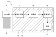
- FIG. 1 is a schematic diagram showing a configuration example of an energy harvester according to a first embodiment of the present technology
- FIG. 3 is a block diagram showing a functional configuration example of an energy harvester
- FIG. 4 is a schematic diagram for explaining a magnetic field generated in a target object
- It is a schematic diagram which shows the structural example of a coil part.
- FIG. 3 is a schematic diagram showing a configuration example of a core of a coil section; Data mapping the magnetic field passing through the drum-shaped core. It is a graph which shows the relationship between the position of a metal, and the Q value of a coil part.
- It is a circuit diagram which shows an example of a rectifier circuit.
- FIG. 4 is a table showing forward voltages and reverse currents of rectifying diodes;
- Figure 10 is a graph of IV measurements for the rectifying diode shown in Figure 9;
- It is a schematic diagram which shows the usage example of an energy harvester. It is a figure which shows an example of the concrete structure and characteristic of a coil part.
- 5 is a graph showing Vf-If characteristics of a backflow prevention diode;
- FIG. 11 is a perspective view showing a configuration example of a core of a coil portion according to a second embodiment;
- FIG. 15 is a schematic diagram showing a configuration example of an energy harvester equipped with the core shown in FIG. 14;
- FIG. 11 is a schematic diagram showing a configuration example of an energy harvester according to a third embodiment
- 3 is a block diagram showing a functional configuration example of an energy harvester
- FIG. It is a schematic diagram for demonstrating operation
- FIG. 4 is a schematic diagram showing a configuration example of a second antenna conductor formed on a circuit board;
- FIG. 11 is a schematic diagram showing a configuration example of an energy harvester according to a fourth embodiment;
- FIG. 11 is a block diagram showing a functional configuration example of an energy harvester according to a fifth embodiment; 4 is a circuit diagram showing an example of connection of a coil section and an antenna section to a rectifying circuit;
- FIG. 3 is a circuit diagram showing a configuration example of an energy harvester having a separation section
- FIG. 4 is a circuit diagram showing another configuration example of an energy harvester having a separation section
- 4 is a circuit diagram showing a configuration example of a filter section
- FIG. 3 is a schematic diagram showing an example of a device equipped with an energy harvester having a separation unit
- FIG. 3 is a schematic diagram showing an example of a device equipped with an energy harvester having a separation unit
- FIG. 3 is a schematic diagram showing an example of a device equipped with an energy harvester having a separation unit
- FIG. 2 is a circuit diagram showing an example of a grounding circuit of a device equipped with an energy harvester
- FIG. 2 is a circuit diagram showing an example of a grounding circuit of a device equipped with an energy harvester;
- FIG. 2 is a circuit diagram showing an example of a grounding circuit of a device equipped with an energy harvester;
- FIG. 3 is a circuit diagram showing a configuration example of an earth leakage countermeasure circuit;
- 1 is a circuit diagram showing a configuration example of an energy harvester compatible with high voltage;
- FIG. 3 is a circuit diagram showing a configuration example of an ideal diode;
- FIG. FIG. 4 is a circuit diagram showing another configuration example of the energy harvester;
- FIG. 4 is a circuit diagram showing another configuration example of the rectifier circuit;
- FIG. 1 is a schematic diagram showing a configuration example of an energy harvester according to a first embodiment of the present technology.
- FIG. 2 is a block diagram showing a functional configuration example of the energy harvester 100.
- the energy harvester 100 is a device that extracts magnetic field energy generated around a metal body, a human body, or the like and harvests it as electric power. That is, it can be said that the energy harvester 100 is a device that performs environmental power generation using magnetic field energy in the surrounding environment.
- an object 1 a metal object or a human body from which magnetic field energy is extracted by the energy harvester 100 is referred to as an object 1 .
- the energy harvester 100 has a coil section 10, a housing 11, a non-magnetic material 12, and a circuit section 13. Further, as shown in FIG. 2 , circuit section 13 includes rectifier circuit 14 , power storage section 15 , power storage element 16 , and load 17 . At least the rectifier circuit 14 is provided in the circuit section 13 . Also, the power storage unit 15, the power storage element 16, and the load 17 may be provided separately from the circuit unit 13, for example, and may be connected as appropriate.
- the coil unit 10 is a coil that takes in magnetic field energy and outputs it as electric power.
- the coil portion 10 has a core 20 made of a magnetic material and a wire rod 21 wound around the core 20 .
- An axis O is set in the coil portion 10 .
- This axis O is the coil axis passing through the center of the loop formed by the wire rod 21 wound around the core 20 .
- the housing 11 is a case that accommodates the coil section 10 .
- the housing 11 functions as a member that holds the coil section 10 with respect to the target object 1 .
- the housing 11 holds the coil section 10 on the surface of the subject 1 such that the axis O of the coil section 10 intersects the surface of the subject 1 including a metal body or a human body.
- the magnetic field generated across the surface of the object 1 passes through the loop formed by the wire rod 21 of the coil section 10, and changes in the magnetic field can be reliably detected.
- the housing 11 corresponds to the holding section. The coil section 10 and the housing 11 will be described later in detail.
- the non-magnetic body 12 is a member made of a non-magnetic material, typically made of a non-magnetic metal.
- the non-magnetic body 12 is arranged at a predetermined distance from the coil section 10 .
- a plate-shaped member is used as the non-magnetic body 12 .
- the distance between the non-magnetic material 12 and the coil portion 10 is set, for example, within a range in which the coil portion 10 can exhibit the required characteristics. The relationship between the non-magnetic material 12 and the coil portion 10 will be described later in detail.
- the circuit unit 13 includes the rectifier circuit 14, the power storage unit 15, the power storage element 16, and the load 17 as described above. Also, the circuit section 13 is arranged on the opposite side of the coil section 10 with the non-magnetic material 12 interposed therebetween. As shown in FIG. 1, the circuit section 13 has a circuit board 40 on which a plurality of circuits such as the rectifier circuit 14 are formed. A non-magnetic material 12 is arranged between the circuit board 40 and the coil section 10 . More specifically, the circuit board 40 is connected to the surface of the non-magnetic body 12 opposite to the coil portion 10 . Note that in FIG. 2 , the non-magnetic material 12 is schematically illustrated as a hatched area surrounding each part of the circuit part 13 .
- the rectifier circuit 14 is a circuit that rectifies the output of the coil section 10 .
- the coil unit 10 outputs AC power in accordance with changes in magnetic flux.
- the rectifier circuit 14 rectifies AC power and converts it into DC power.
- the rectifier circuit 14 corresponds to a rectifier.
- the coil unit 10 and the rectifier circuit 14 constitute a power receiver that receives magnetic field energy generated around the object 1 as power.
- the power storage unit 15 is a circuit that charges the power storage element 16 .
- the power storage unit 15 charges the power storage element 16 with the power output from the rectifier circuit 14 .
- the power storage unit 15 outputs electric power necessary for charging, for example, according to the state of charge of the power storage element 16 .
- the electric power charged in the storage element 16 may be, for example, the output of the rectifier circuit 14 itself, or may be electric power stored in a capacitor or the like.
- the power storage element 16 is an element that stores power rectified by the rectifier circuit (power received by the coil section 10), and supplies the power to the load 17 as needed.
- a capacitor, a secondary battery, or the like, for example, is used as the storage element 16 .
- the energy harvester 100 functions as a charging device that charges the storage element 16 with the output of the coil section 10 via the rectifier circuit 14 and the storage section 15 .
- the load 17 is a circuit or element driven by the electric power of the storage element 16 .
- a control unit such as a microcomputer, a communication unit, various sensors, and the like are used as the load 17 .
- FIG. 3 is a schematic diagram for explaining the magnetic field generated in the object 1.
- the electric current 2 flowing through the object 1 is schematically illustrated by dotted arrows.
- the direction of the dotted arrow indicates the direction of the current.
- a magnetic field 3 generated by the current 2 is schematically illustrated by solid arrows.
- the direction of the solid arrow indicates the direction of the magnetic field 3 (magnetic flux).
- a magnetic field 3 corresponding to the current 2 is generated around the object 1 through which the current 2 flows.
- the direction of the magnetic field 3 is also reversed.
- a potential difference is basically generated with respect to the potential of the earth unless it is forcibly grounded to the earth GND (earth ground 4).
- most home electric appliances convert alternating current power into direct current power for use. For example, when converting power from alternating current to direct current, pulse signals with positive (+) and negative (-) potentials may be generated.
- home appliances use various clock frequencies for power conversion and the like, and the GND itself provided in the circuit of the home appliance may fluctuate. As a result, a potential difference is generated between the home appliance and the earth ground 4, and AC currents of various frequencies flow through the home appliance.
- the object 1 is floating from the earth ground 4 and an alternating current 2 is flowing.
- This can also be said to be a state in which a virtual AC power supply 5 is connected between the object 1 and the earth ground 4, as shown in FIG.
- a current 2 flowing through the object 1 is a current whose direction changes alternately.
- This current 2 is, for example, a product obtained by superimposing alternating currents of various frequencies.
- an upward magnetic field 3 is generated in the drawing.
- a downward magnetic field 3 is generated in the drawing.
- the direction of the current 2 changes again, and when the current 2 flows from the left side to the right side in the drawing as in #3, an upward magnetic field 3 is generated in the same manner as in the case of #1.
- an alternating magnetic field 3 is generated in a direction penetrating the surface of the object 1 due to the alternating current 2 flowing through the object 1 .
- the magnetic field 3 generated by the current 2 exhibits, for example, an annular distribution rotating around the current 2 . Therefore, depending on where the magnetic field 3 is generated, the relationship between the direction of the current 2 and the direction of the magnetic field 3 shown in FIG. 3 may be reversed.
- an alternating current 2 is induced in the object 1 and a magnetic field 3 is generated around the object 1 .
- the electric field acting on the object 1 includes electric fields of various frequencies, such as radio waves propagating around the object 1 and quasi-electrostatic fields generated around the object 1 . These electric fields can induce alternating currents 2 even in objects 1 that are not connected to an alternating current source, such as a human body or a metal shelf. In this case, a magnetic field 3 is generated around the object 1 according to the current 2 induced by the electric field.
- the object 1 may be, for example, an object in which an alternating current 2 is induced and a magnetic field 3 is generated.
- the object 1 includes a metal object or a human body.
- Metal objects are industrial products (cars, vending machines, refrigerators, microwave ovens, metal racks, guardrails, mailboxes, traffic lights, etc.) and objects made of metal. It is in a state of floating from the earth ground 4.
- the metal body may be made of any metal such as iron, aluminum, copper, metal alloy, etc., and the material is not limited as long as it is metal.
- the energy harvester 100 is configured for such magnetic field energy. The configuration of each part of the energy harvester 100 will be specifically described below.
- FIG. 4 is a schematic diagram showing a configuration example of the coil section 10. As shown in FIG. The coil portion 10 is configured by winding a wire rod 21 around a core 20 . Wire 21 may be directly wound around core 20 , or another member may be provided between core 20 and wire 21 . For example, when forming the housing 11 made of resin using a technique such as molding, it is possible to cover the entire core 20 with resin. In this case, wire rod 21 is wound around core 20 coated with resin.
- the core 20 of the coil section 10 is configured using a magnetic material.
- the core 20 with high magnetic permeability is arranged inside the coil, and the Q value of the coil is improved.
- the Q value of the coil is an index showing the relationship between energy retention and loss in the coil. For example, the higher the Q value, the smaller the energy loss. Therefore, by increasing the Q value of the coil section 10, it is possible to efficiently take in the magnetic field energy.
- the magnetic material forming core 20 is soft ferrite.
- Soft ferrite is an insulating ceramic with soft magnetic properties.
- Soft ferrite is characterized by a small coercive force that retains magnetic force and a high magnetic permeability. Therefore, when the external magnetic field disappears, the magnetic force disappears, but while the external magnetic field is acting, the magnetic flux density increases and it is strongly magnetized.
- Soft ferrite can also be magnetized in response to magnetic fields over a wide frequency range. Therefore, by using the core 20 made of soft ferrite, it is possible to efficiently capture magnetic field energy in a wide frequency range. This greatly improves the efficiency of capturing the magnetic field energy.
- the soft ferrite constituting the core 20 is made of a material having a high magnetic permeability at the frequency of the magnetic field to be taken in, for example. Therefore, the type of soft ferrite is selected according to the frequency of noise (AC current) to be received.
- AC current the frequency of noise
- Mn—Zn based soft ferrite is used for frequencies in the range of 50 Hz to several MHz.
- Ni—Zn soft ferrite is used.
- Mn--Zn soft ferrite having high magnetic permeability is used.
- Ni--Zn-based soft ferrite is used for the object 1 in which an alternating current of several MHz or more is induced.
- the wire material 21 of the coil part 10 is, for example, a litz wire that is formed into one electric wire by twisting a plurality of thin wires each of which is insulated.
- a specific configuration of the wire rod 21 is not limited, and for example, a single wire rod 21 may be used.
- the wire rod 21 is wound a predetermined number of turns around the core 20 (an axial core portion 23 to be described later).
- the winding method of the wire rod 21 is alpha winding. That is, the wire rod 21 becomes an alpha winding.
- Alpha winding is a winding method in which the wire rod 21 at the winding start and the winding end is wound around the outer circumference of the coil.
- an alpha winding is configured by winding both ends of the wire rod 21 outward at the same time. This prevents one end of the wire 21 from being left inside the winding, improves the space factor of the wire 21, and improves the coil performance such as the Q value.
- the method of winding the wire 21 is not limited to alpha winding, and other winding methods may be used.
- the core 20 is formed using a magnetic material (here, soft ferrite), and the litz wire is wound around the core 20 (axial core portion 23) by alpha winding to improve the Q value. ing. Both ends of the wire 21 are hereinafter referred to as a first coil terminal 21a and a second coil terminal 21b, respectively.
- FIG. 5 is a schematic diagram showing a configuration example of the core 20 of the coil section 10.
- the core 20 has a shaft portion 23 and a pair of flange portions 24 .
- the core portion 23 is a portion around which the wire rod 21 is wound, and is a solid member that fills the inside of the loop formed by the wire rod 21 .
- the axial core portion 23 has a columnar shape extending along the axis O of the coil portion 10, and the wire rod 21 is wound along the side surface thereof.
- a cylindrical shape, a polygonal prism shape such as a square prism shape, an elliptical shape, or the like is used.
- the pair of flange portions 24 are provided at both ends of the shaft core portion 23 and form flanges projecting outward from the side surfaces of the shaft core portion 23 . Therefore, the core 20 has a drum-shaped (H-shaped) shape in which the shaft core portion 23 is sandwiched between the pair of flange portions 24 .
- the planar shape of each flange portion 24 is, for example, a circular shape, a polygonal shape such as a quadrangle, an elliptical shape, or the like.
- the planar shape of the flange portion 24 may be a shape obtained by enlarging the cross-sectional shape of the axial core portion 23 or a shape matching the shape of the housing 11 or the like. Note that the flange portion 24 does not necessarily have to be provided, and for example, the core 20 may have a structure without the flange portion 24 .
- the housing 11 holds the coil part 10 so that one of the pair of flange parts 24 faces the target object 1 .
- the flange portion 24 directed toward the target object 1 is referred to as a first flange portion 24a
- the portion 24 is described as a second flange portion 24b.
- the lower flange portion 24 and the upper flange portion 24 in the drawing are referred to as a first flange portion 24a and a second flange portion 24b, respectively.
- the core 20 of the coil portion 10 also has a first end face 25a facing the target object 1 and a second end face 25b opposite to the first end face 25a.
- the surface of the first flange portion 24a opposite to the side connected to the axial core portion 23 serves as the first end surface 25a.
- the surface of the second flange portion 24b opposite to the side connected to the shaft core portion 23 serves as a second end surface 25b.
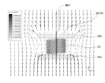
- FIG. 6 is data mapping the magnetic field passing through the drum-shaped core 20 .
- Arrows representing magnetic flux are mapped on a plane passing through the axis O of the coil section 10 .
- the direction of each arrow represents the direction of the magnetic field at each point, and the color of each arrow represents the strength (A/m) of the magnetic field at each point.
- a wire rod 21 is wound around the core 20 to form the coil portion 10 . It is also assumed that the axis O of the coil portion 10 is oriented in the vertical direction (Z direction) in the drawing, and that an external magnetic field is generated in the upward direction in the drawing. Therefore, the magnetic flux entering the core 20 from the lower first flange portion 24 a of the core 20 escapes from the upper second flange portion 24 b of the core 20 .
- the direction of the magnetic flux is bent so as to concentrate on the first flange portion 24a projecting outward from the axial core portion 23.
- the direction of the magnetic flux is bent so as to spread from the second flange portion 24b projecting outward from the axial core portion 23.
- the direction of the magnetic flux is bent so that the magnetic flux concentrates on the axial core portion 23 .
- the housing 11 has a first end 26a, a second end 26b and a side 27.
- the first end portion 26a and the second end portion 26b are plate-shaped members arranged perpendicular to the axis O of the coil portion 10 and facing each other.
- the side portion 27 is a plate-like member extending along the axis O of the coil portion 10 and connects the first end portion 26a and the second end portion 26b.
- a U-shaped housing 11 is configured in which a first end portion 26a and a second end portion 26b protrude in the same direction from both ends of a plate-shaped side portion 27. be.
- the housing 11 accommodates the coil section 10 .
- the housing 11 is configured such that at least part of the coil section 10 is accommodated inside the housing 11 or in the space formed by the housing 11 .
- the first flange portion 24a is embedded inside the first end portion 26a
- the second flange portion 24b is embedded inside the second end portion 26b.
- the axial core portion 23 around which the wire rod 21 is wound is arranged in the space sandwiched between the first end portion 26a and the second end portion 26b.
- the coil section 10 is accommodated in the gap formed in the U-shaped housing 11 .
- the housing 11 is made of, for example, a resin material such as plastic, and is formed using a technique such as molding. In this case, the housing 11 is formed by filling the resin material with the core 20 placed in the mold. Alternatively, the configuration may be such that the core 20 is fitted after the housing 11 is formed. Further, the configuration of the housing 11 is not limited to the example shown in FIG. For example, the housing 11 may be constructed so as to cover the entire core 20 including the axial core portion 23 . In this case, the wire rod 21 is wound around the resin material covering the shaft core portion 23 . Moreover, the housing 11 may be configured such that the core 20 around which the wire rod 21 is wound is covered with a resin material.
- the housing 11 is attached to the surface of the target object 1 . That is, the housing 11 is configured to be fixed in contact with or in close proximity to the surface of the target object 1 .
- a mounting surface 28 is the surface that contacts or approaches the surface of the target object 1 .
- the mounting surface 28 is the surface facing the outside of the plate-like first end portion 26 a (the side opposite to the second end portion 26 b ).
- the mounting surface 28 is basically a flat surface, but may have a curved shape such as a concave surface or a convex surface according to the shape of the surface of the object 1, for example.
- the housing 11 is provided with a mounting mechanism (not shown) for mounting on the surface of the target object 1 .
- a mounting mechanism (not shown) for mounting on the surface of the target object 1 .
- Bands, adhesive tapes, screwing mechanisms, magnets, clips, fitting grooves, suction cups, adhesives, etc. are used as mounting mechanisms.
- any fixture that can attach the housing 11 to the surface of the target object 1 may be used.
- the housing 11 is fixed with the mounting surface 28 in contact with the exterior of the home appliance or the like.
- the housing 11 is formed in a size that can be worn by a human body, and is fixed with the mounting surface 28 in contact with the skin of the human body or the surface of clothing.
- the housing 11 holds the coil section 10 so that the axis O of the coil section 10 and the mounting surface 28 are perpendicular to each other.
- the coil section 10 can be arranged with the axis O of the coil section 10 orthogonal to the surface of the target object 1 .
- the magnetic field created by the current flowing through the object 1 is orthogonal to the direction of current flow. Therefore, in the vicinity of the surface of the target object 1, a magnetic field is mainly generated in a direction orthogonal to the surface of the target object 1.
- FIG. Therefore, the direction in which the magnetic field changes is the direction perpendicular to the surface of the object 1 (normal direction to the surface of the object 1).
- the axis O of the coil section 10 is orthogonal to the surface of the target object 1, and the direction in which the magnetic field changes and the axis O of the coil section 10 are aligned. will match. This makes it possible to take in the magnetic field energy without waste.
- the housing 11 includes the coil section 10 so that the end surface (first end surface 25a) of the core 20 directed toward the target object 1 and the mounting surface 28 are aligned in the direction of the axis O of the coil section 10. may be retained. Therefore, the housing 11 may be configured such that the first end surface 25a of the first flange portion 24a is exposed and functions as the mounting surface 28 . Alternatively, a configuration may be adopted in which the first end surface 25a protrudes from the housing 11 toward the target object 1 side. As a result, the distance between the surface of the object 1 and the core 20 is close, and the magnetic field can be collected at a position where the magnetic field is strong (the magnetic flux density is large), and the magnetic field energy can be efficiently captured.
- the non-magnetic body 12 is a plate-like or sheet-like member arranged at a certain distance from the coil portion 10 . As shown in FIG. 1 , a side portion 27 of the housing 11 has a side surface 29 opposite to the coil portion 10 . The non-magnetic body 12 is fixed to the side surface 29 of this housing 11 .
- the method for fixing the non-magnetic body 12 to the side surface 29 is not limited, and methods such as adhesion, screwing, and fitting may be used. In this configuration, the distance between the side surface 29 of the housing 11 and the coil portion 10 (for example, the distance from the axis O of the coil portion 10 to the side surface 29) is the distance between the coil portion 10 and the non-magnetic material 12.
- the non-magnetic material 12 is capable of causing a magnetic field (magnetic flux) to flow at a position separated from the coil section 10 by a certain distance. As a result, the magnetic field around the coil section 10 is prevented from being absorbed by other metals included in the circuit section 13, and the effect of keeping the flow of the magnetic field properly is exhibited. In addition, since the non-magnetic material 12 has less loss of magnetic field energy due to eddy currents than ferromagnetic metal, it is possible to sufficiently suppress deterioration of the Q value. By covering the coil section 10 with the non-magnetic material 12 at a certain distance from the coil section 10 in this manner, the influence of the circuit section 13 can be reduced.
- the non-magnetic material 12 is configured so as to be able to cover the surface of the circuit board 40 to be described later facing the coil section 10 . Therefore, from the circuit board 40 side, the coil section 10 is completely blocked by the non-magnetic material 12 and cannot be seen.
- the non-magnetic body 12 is configured to have the same shape and size as the circuit board 40 .
- the non-magnetic body 12 may be configured to have a planar shape larger than that of the circuit board 40 . This makes it possible to sufficiently reduce the influence of the metal contained in the circuit board 40 (circuit section 13 ) on the coil section 10 .
- the non-magnetic body 12 is arranged parallel to the axis O of the coil portion 10 .
- the side surface 29 of the housing 11 is configured as a surface parallel to the axis O of the coil section 10
- the non-magnetic material 12 is arranged along the side surface 29 .
- the side surface 29 is inclined with respect to the axis O of the coil unit 10
- the magnetic field distributed along the axis O of the coil portion 10 can flow without significantly changing the direction of the magnetic field. It becomes possible to sufficiently suppress deterioration of the Q value of 10. Further, by setting the non-magnetic body 12 in a posture parallel to the axis O of the coil section 10, even if the non-magnetic body 12 is brought close to the coil section 10, the Q value and the like are hardly affected. This makes it possible to make the device size compact.
- Aluminum is typically used as the non-magnetic material 12 . This makes it possible to reduce the weight of the device. Copper may also be used as the non-magnetic material 12 . In addition, any non-magnetic metal may be used. Further, in this embodiment, a plate member having a thickness of 0.3 mm or more, for example, is used as the non-magnetic body 12 . A thickness of about 0.3 mm can sufficiently suppress deterioration of the Q value of the coil portion 10 . Of course, a non-magnetic material 12 with a thickness of 0.5 mm or 1 mm may be used. Also, a non-magnetic material 12 having a thickness of less than 0.3 mm may be used as long as the decrease in the Q value is within an allowable range.
- FIG. 7 is a graph showing the relationship between the distance between the plate (non-magnetic material 12) using a non-magnetic material metal and the coil portion 10 and the Q value.
- the horizontal axis of the graph is the distance between the metal and the side surface of the coil portion 10 .
- the vertical axis of the graph is the Q value of the coil section 10 .
- the data shown in FIG. 7 is obtained by measuring the Q value by changing the positions of the aluminum (Al) plate and the stainless steel (SUS) plate. The thickness of the measured plate was 0.5 mm in all cases, and measurements were made on plates of 7 mm x 20 mm and 90 mm x 30 mm for each material.
- the Q value of the coil portion 10 tends to deteriorate when there is a metal plate nearby, and the Q value deteriorates as the area of the metal plate increases.
- aluminum has less deterioration of the Q value than stainless steel. This is because a single non-magnetic material such as aluminum or copper does not accumulate magnetic lines of force in comparison to stainless steel, which is made mainly of iron, which is a magnetic material, so eddy currents are less likely to flow.
- stainless steel which is made mainly of iron, which is a magnetic material
- the distance between the non-magnetic body 12 and the coil portion 10 is set so that the deterioration of the Q value falls within an allowable range.
- the Q value of the coil section 10 can be measured using, for example, an LCR meter, a Q meter, or the like.
- the arrangement distance between the non-magnetic body 12 and the coil section 10 is, for example, a distance such that the Q value of the coil section 10 is 20% to 30% lower than the Q value when the non-magnetic body 12 is not arranged. is set to As a result, the device size can be made compact while maintaining a sufficient Q value. Further, for example, the distance may be set so that the amount of deterioration from the Q value when the non-magnetic material 12 is not arranged is 10% or less. This makes it possible to sufficiently improve the efficiency of capturing the magnetic field energy.
- the non-magnetic material 12 does not necessarily need to be provided.
- the circuit section 13 is provided separately from the housing 11 that accommodates the coil section 10, and there is no metal that blocks the magnetic field near the coil section 10, the non-magnetic material 12 may not be provided.
- the circuit section 13 has a flat circuit board 40 arranged along the non-magnetic body 12 .
- the circuit board 40 is made of glass epoxy or the like, and is a mounting board on which various circuits are provided. or placed in close proximity.
- the circuit board 40 includes a rectifier circuit 14, a power storage unit 15, and a power storage element 16 for operating the energy harvester 100, various sensors serving as a load 17, and BLE (Bluetooth (registered (trademark) Low Energy) and other communication devices are provided.
- BLE Bluetooth (registered (trademark) Low Energy)
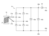
- FIG. 8 is a circuit diagram showing an example of a rectifier circuit.
- the rectifier circuit 14 is configured as a full-wave rectifier circuit.
- the rectifier circuit 14 has four diodes 41a to 41d, two Zener diodes 42a and 42b, an anti-backflow diode 43, and output terminals 45a and 45b.
- the diode 41a and the diode 41b are connected in series with the diode 41a leading in the forward direction.
- a connection point 44a is provided between the diode 41a and the diode 41b.
- the diode 41c and the diode 41d are connected in series with the diode 41c leading in the forward direction.
- a connection point 44b is provided between the diode 41c and the diode 41d.
- a cathode of each of the diode 41 a , the diode 41 c , the Zener diode 42 a and the Zener diode 42 b is connected to the anode of the backflow prevention diode 43 .
- a cathode of the backflow prevention diode 43 is connected to the output terminal 45a.
- Each anode of the diode 41b, the diode 41d, the Zener diode 42a, and the Zener diode 42b is connected to the output terminal 45b.
- a first coil terminal 21a of the coil section 10 is connected to a connection point 44a between the diodes 41a and 41b.
- a second coil terminal 21b of the coil section 10 is connected to a connection point 44b between the diodes 41c and 41d.
- the AC magnetic field detected by the coil section 10 is output from the first and second coil terminals 21a and 21b as AC power.
- This alternating current power is full-wave rectified by four diodes 41a to 41d and output as direct current power from output terminals 45a and 45b.
- the rectifier circuit 14 shown in FIG. 8 is configured using the minimum diodes 41a to 41d required for full-wave rectification. As a result, unnecessary leakage current is suppressed, and the efficiency of capturing magnetic field energy can be sufficiently improved.
- the Zener diode 42a is an element for releasing static electricity or the like applied to, for example, the first and second coil terminals 21a and 21b.
- the Zener diode 42a functions as an electrostatic protection component that releases static electricity.
- the Zener diode 42b is, for example, an element for protecting the subsequent IC circuit (power storage unit 15, etc.) connected to the output terminals 45a and 45b.
- the Zener diode 42b functions as a low resistance conductor. As a result, it becomes possible to avoid a situation in which the subsequent circuit is damaged.
- the backflow prevention diode 43 is a diode that prevents backflow of current. By providing the anti-backflow diode 43, it is possible to suppress the backflow of current when the voltage of the coil section 10 drops, and to stably operate the subsequent circuit.
- the configuration of the rectifier circuit 14 is not limited.
- a voltage doubler rectifier circuit that doubles the voltage using a capacitor, a quadruple voltage rectifier circuit, a rectifier circuit incorporating a Cockcroft-Walton circuit, or the like may be used.
- a half-wave rectifier circuit or the like may be used.
- the rectifier circuit 14 may be appropriately configured according to the power reception characteristics of the coil section 10, the characteristics of the elements and circuits used as the load 17, and the like.
- FIG. 9 is a table showing forward voltage Vf and reverse current Is of a rectifying diode.
- FIG. 10 is a graph of IV measurements for the rectifying diode shown in FIG. Silicon and germanium diodes were measured as a rectifying diode product number 1N60, and another product number ISS108 was evaluated using a germanium diode manufactured by a different manufacturer.
- curve (a) is the characteristic of 1N60 (silicon)
- curve (b) is the characteristic of 1N60 (germanium)
- curve (c) is the characteristic of ISS108 (germanium).
- the current that flows when a voltage is applied in the reverse direction of the diode is the reverse current Is.
- the measurement data in FIG. 9 are data when 10 V is applied in the reverse direction of the diode.
- the forward voltage Vf is the voltage when the forward current (1 mA) begins to flow through the diode.
- the diode 1N60 silicon
- the reverse current Is when the forward voltage Vf of the diode is applied in the reverse direction was evaluated. Considering that the reverse current Is shown in FIG. Yes, 1N60 (germanium) is 0.21 ⁇ A and ISS108 (germanium) is 0.5 ⁇ A.
- 1N60 (silicon) is 1/27778, 1N60 (germanium) is 1/4762, and ISS108 (germanium) is 1/2000. That is, the rectifying diodes (41a to 41d) used in the rectifying circuit 14 need to have a ratio of about 4700 times or more, preferably 10000 or more. As a result, of the three example diodes, 1N60 (silicon) has the most suitable characteristics.
- the reverse current Is when applied in the reverse direction is preferably small.
- 1N60 (germanium) is 1.43 M ⁇ and ISS108 (germanium) is 0.38 M ⁇ .
- the resistance value for preventing the current from flowing in the reverse direction is large. is required, preferably 10 M ⁇ or more.
- 1N60 (silicon) has the most suitable characteristics.
- FIG. 11 is a schematic diagram showing an example of use of the energy harvester.
- an energy harvester 100 is attached to the exterior of a target object 1, which is a refrigerator 1a, which is a home appliance.
- the exterior of the refrigerator 1a is configured using, for example, a metal plate or the like, and the energy harvester 100 is attached using a magnet or the like.
- the refrigerator 1a also includes a portion (for example, an exterior, a frame, etc.) that floats with respect to the ground GND (earth ground 4).
- GND earth ground 4
- an AC current is induced in the refrigerator 1a in accordance with a household AC power supply or the like, and an AC magnetic field is generated on the surface of the refrigerator 1a. This magnetic field is captured as power by the energy harvester 100 .
- the energy harvester 100 is attached to the legs (frames) of the target object 1, which is a steel rack 1b that is a metal object.
- the steel rack 1b is arranged on the carpet 38 and is in a state of floating from the earth ground 4.
- electric fields such as radio waves propagating around the steel rack 1b and power source noise act on the steel rack 1b to induce an alternating current, and an alternating magnetic field is generated on the surface of the steel rack 1b. This magnetic field is captured as power by the energy harvester 100 .
- the human body 1c is used as the target body 1, and the energy harvester 100 is attached to the wrist of the human body 1c using a band or the like.
- the human body 1 a is wearing shoes or the like, and is in a state of floating from the earth ground 4 .
- radio waves propagating around the human body 1a, an electric field generated by walking, and the like act on the human body 1a to induce an alternating current, and an alternating magnetic field is generated on the surface of the human body 1a. This magnetic field is captured as power by the energy harvester 100 .
- FIG. 12 is a diagram showing an example of the specific configuration and characteristics of the coil section.
- a coil portion 10 shown in FIG. 12 is a thin coil using a drum-shaped core 20 having a circular planar shape when viewed in the direction of the coil axis.
- a Mn--Zn based ferrite core is used to receive low frequency power.
- the overall height (outer width) h1 of the core 20 is 3.3 mm
- the thickness w1 of the first flange portion 24a and the thickness W2 of the second flange portion 24b are both 0.3 mm. 6 mm
- the height (inner width) of the core portion 23 around which the wire rod 21 is wound is 2.1 mm.
- the diameter d1 of the core 20 as a whole (the diameter of the first flange portion 24a and the second flange portion 24b) is 25 mm ⁇
- the diameter d2 of the axial core portion 23 is 19 mm ⁇ .
- a litz wire having a wire diameter of 0.65 mm was wound around the axial core portion 23 of the core 20 by alpha winding to form the coil portion 10 .
- the number of windings of the litz wire was 3 stages and 6 layers.
- FIG. 12B shows the characteristics of the coil section 10 shown in FIG. 12A.
- the coil part 10 is measured alone without providing the non-magnetic material 12 .
- An LCR meter was used for this measurement, the measurement frequency was 120 kHz, and the measurement current was 1 mA.
- the inductance Ls of the coil portion 10 was 29.5 ⁇ H and the Q value was 118.8.
- the equivalent series resistance Rs of the coil portion 10 was 0.186 ⁇ , and the DC resistance Rdc was 0.127 ⁇ .
- the inventor mounted the coil portion 10 shown in FIG. 12 on the exterior of the refrigerator 1 and conducted an experiment in which electric power was harvested using the rectifier circuit 14 shown in FIG.
- the secondary battery which is the storage element 16
- the secondary battery was connected between the output terminals 45a and 45b of the rectifier circuit 14, and the secondary battery was directly charged via the backflow prevention diode 43.
- FIG. During charging the voltage V1 between output terminals 45a and 45b was 2.300V.
- the output voltage V2 of the rectifier circuit 14 before passing through the backflow prevention diode 43 here, the voltage between the detection point 46a on the cathode side and the detection point 46b on the anode side of the Zener diode 42b
- the voltage drop due to the backflow prevention diode 43 is about 0.144V.
- FIG. 13 is a graph showing Vf-If characteristics of a backflow prevention diode.
- FIG. 13 shows the relationship between the forward voltage Vf and the forward current If of the backflow prevention diode 43 for each measurement temperature (100° C., 75° C., 50° C., 25° C., 0° C., ⁇ 25° C.). ing.
- the horizontal axis of the graph is the forward voltage Vf applied to the anti-backflow diode 43
- the vertical axis of the graph is the forward current If flowing through the anti-backflow diode 43 .
- the coil portion 10 is held with the axis O intersecting with the surface of the target object 1 including a metal object or a human body. Further, the output of the coil section 10 is rectified and used as electric power. A core 20 of the coil portion 10 is made of a magnetic material. Therefore, the magnetic flux generated around the object 1 can be collected. This makes it possible to efficiently take in the magnetic field energy generated in the surrounding environment.
- FIG. 14 is a perspective view showing a configuration example of the core of the coil portion according to the second embodiment.
- FIG. 15 is a schematic diagram showing a configuration example of an energy harvester on which the core 51 shown in FIG. 14 is mounted.
- the core 51 of the coil portion 50 is configured such that the periphery of the axial core portion 53 is covered with a magnetic material.
- the core 51 has a shaft portion 53 , a flange portion 54 and side wall portions 55 .
- the core 51 is entirely made of a magnetic material (typically soft ferrite).
- the shaft core portion 53 is a portion around which the wire rod 21 is wound, and is a solid member that fills the inside of the loop formed by the wire rod 21 .
- a cylindrical shaft core portion 53 is configured.
- the shape of the shaft core portion 53 is not limited, and any columnar shape may be used.
- the flange portion 54 is a portion that is provided at one end of the shaft core portion 53 and protrudes outward from the side surface of the shaft core portion 53 .
- the flange portion 54 having a square planar shape is formed, and the shaft core portion 53 is connected so that the central axis of the shaft core portion 53 (the axis O of the coil portion 50) passes through the center of the flange portion 54 .
- the planar shape of the flange portion 54 is not limited.
- the side wall portion 55 is a portion that is connected to the flange portion 54 and that surrounds at least a portion of the shaft core portion 53 while being spaced apart from the shaft core portion 53 . That is, the side wall portion 55 protrudes from the surface of the flange portion 54 to which the shaft core portion 53 is connected, and forms a wall surrounding the shaft core portion 53 at a position away from the shaft core portion 53 .
- the flange portion 54 having a square planar shape has side wall portions 55 protruding from three of the four sides forming the outer edge thereof. The distance between the axial core portion 53 and the side wall portion 55 is set so that the wire rod 21 can be wound at least a desired number of turns.
- FIG. 15A and 15B schematically show cross-sectional views of energy harvesters 200a and 200b configured using the core 51 shown in FIG.
- the circuit section 36 formed on the non-magnetic material 35 is directly arranged on the core 51 of the coil section 50.
- the present invention is not limited to this, and the coil section 50 (core 51) may be accommodated in a predetermined housing, and the non-magnetic material 35 and the circuit section 36 may be arranged on the housing.
- the energy harvesters 200a and 200b have the same configuration of the coil section 50 (core 51), but the positions of the non-magnetic material 35 and the circuit section 36 are different.
- the coil portion 50 is arranged such that the other end of the axial core portion 53 (the side opposite to the side where the flange portion 54 is provided) faces the target object 1 .
- the surface of the coil section 50 on the lower side in the drawing faces the target object 1 .
- the coil section 50 is directly held by using a predetermined mounting mechanism as a holding section so that the other end of the axial core section 53 faces the target object 1 .
- the coil portion 50 is accommodated in the housing, the coil portion 50 is held by using the housing as a holding portion so that the other end of the axial core portion 53 faces the target object 1 .
- the surface formed at the other end of the shaft core portion 53 is the first end face 56 a facing the target object 1 , and the side of the flange portion 54 connected to the shaft core portion 53 . is the second end face 56b.
- the shaft core portion 53 surrounded by the side wall portion 55 is exposed, and magnetic flux is easily taken in.
- magnetic flux tends to pass through the interior of magnetic materials. Therefore, by surrounding the axial core portion 53 with the side wall portion 55 and the flange portion 54 made of a magnetic material and directing the first end surface 56a side where the axial core portion 53 is exposed toward the target object 1, The effect of confining the generated magnetic flux is expected.
- This can be said to be a configuration in which the magnetic flux emitted from the target object 1 is limited only to the front side (first end face 56a side) that receives energy.
- the magnetic flux is concentrated on the shaft core portion 53 around which the wire 21 is wound, and the magnetic field energy can be taken in very efficiently.
- the non-magnetic material 35 and the circuit section 36 are arranged in this order on the second end surface 56b of the flange portion 54 opposite to the first end surface 56a. That is, the non-magnetic material 35 and the circuit section 36 are arranged perpendicular to the axis O of the coil section 50 .
- the side wall portion 55 as described above, the magnetic flux is less likely to leak, and even when the circuit portion 36 and the like are arranged on the axis O of the coil portion 50, the Q value is not significantly degraded.
- the non-magnetic material 35 and the circuit portion 36 are arranged in this order on the outer surface 57 of the side wall portion 55 . That is, the non-magnetic material 35 and the circuit section 36 are arranged perpendicular to the axis O of the coil section 50 .
- the non-magnetic material 35 and the circuit portion 36 are provided on the outer surface 57 of the central side wall portion 55 formed in a U shape, but the outer surfaces of the side wall portions 55 formed along the other two sides 57. In this case as well, since the magnetic flux is less likely to leak due to the flange portion 54 and the side wall portion 55, deterioration of the Q value due to the circuit portion 36 can be sufficiently suppressed. Further, in FIG.
- the contact surface that contacts the object 1 may be reversed. That is, the energy harvester 200b may be arranged such that the second end face 56b of the flange portion 54 contacts the surface of the target object 1.
- FIG. in this case, for example, magnetic flux can be collected from a wide range with which the flange portion 54 contacts.
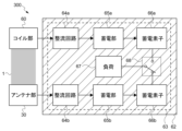
- FIG. 16 is a schematic diagram showing a configuration example of an energy harvester according to the third embodiment.
- FIG. 17 is a block diagram showing a functional configuration example of the energy harvester 300.
- the energy harvester 300 has a configuration in which an antenna section 30 for capturing electric field energy generated in the surrounding environment is provided in addition to the coil section 60 for capturing magnetic field energy.
- the energy harvester 300 has a coil section 60 , a housing 61 , a non-magnetic body 62 , a circuit section 63 and an antenna section 30 .
- the coil section 60, the housing 61, and the non-magnetic body 62 are configured in the same manner as the coil section 10, the housing 11, and the non-magnetic body 12 of the energy harvester 100 shown in FIG. 1, for example. Therefore, the energy harvester 300 shown in FIG. 16 is a device obtained by adding the antenna section 30 to the energy harvester 100 shown in FIG. 1 and changing the circuit configuration.
- the antenna unit 30 functions as a receiving antenna for receiving power through the object 1 including a metal object or a human body.
- the antenna unit 30 receives electric field energy of radio waves and quasi-electrostatic fields in the space around the object 1 as power. Therefore, the energy harvester 300 is a device capable of extracting magnetic field energy using the coil section 60 and extracting electric field energy using the antenna section 30 from the target object 1 such as a metal body or a human body. As a result, since power can be harvested from both the coil section 60 and the antenna section 30, energy can be efficiently harvested.
- the circuit section 63 of the energy harvester 300 has a circuit for the coil section 60 and a circuit for the antenna section 30 .
- a circuit for the coil unit 60 includes a rectifier circuit 64a, a power storage unit 65a, and a power storage element 66a.
- the circuit for the antenna section 30 includes a rectifier circuit 64b, a power storage section 65b, and a power storage element 66b.
- the circuit section 63 further has a switch section 68 and a load 67 .
- the circuitry for coil portion 60 charges the magnetic field energy captured by coil portion 60 .
- the rectifier circuit 64 a rectifies the output of the coil section 60 .
- the coil unit 60 and the rectifier circuit 64a constitute a power receiver that receives the magnetic field energy generated around the object 1 as power.
- the power storage unit 65a charges the power storage element 66a with the power output from the rectifier circuit 64a.
- the power storage element 66a is an element that stores power received by the coil section 60 .
- a charging device for the coil unit 60 is configured to charge the power storage element 66a with the output of the coil unit 60 via the rectifier circuit 64a and the power storage unit 65a.
- a circuit for the antenna section 30 charges the electric field energy captured by the antenna section 30 .
- the rectifier circuit 64 b rectifies the output of the antenna section 30 .
- the antenna unit 30 and the rectifier circuit 64b constitute a power receiver that receives electric field energy generated around the object 1 as power.
- the power storage unit 65b charges the power storage element 66b with the power output from the rectifier circuit 64b.
- the storage element 66b is an element that stores power received by the antenna section 30 .
- a charging device for the antenna section 30 is configured to charge the power storage element 66b with the output of the antenna section 30 via the rectifier circuit 64b and the power storage section 65b.
- the rectifier circuits 64a and 64b are configured similarly to the rectifier circuit 14 described with reference to FIG. 6, for example. 1, and storage elements 66a and 66b are configured, for example, similarly to the storage element 16 in FIG.
- a circuit corresponding to the characteristics of the coil section 60 and the antenna section 30 may be used.
- the rectifier circuit 64a corresponds to a coil rectifier circuit
- the rectifier circuit 64b corresponds to an antenna rectifier circuit.
- a rectifying section is configured by the rectifying circuit 64a and the rectifying circuit 64b.
- the switch unit 68 is a circuit that switches between the power storage element 66 a and the power storage element 66 b to connect to the load 67 .
- the load 67 is a circuit or element such as a sensor driven by the electric power of the storage elements 66a and 66b.
- the switch unit 68 detects, for example, the charging rates of the storage element 66 a and the storage element 66 b and performs control such that the one with the higher charging rate is connected to the load 67 .
- control may be performed to switch the connection of the load to the other storage element.
- the method for switching between the storage element 66a and the storage element 66b is not limited.
- the energy harvested from both the coil section 60 and the antenna section 30 is individually stored in the two storage elements 66a and 66b.
- the stored electric power is switched by the switch unit 68 and supplied to the load 67 .
- the energy harvested by the coil section 60 is magnetic field energy and the energy harvested by the antenna section 30 is electric field energy. Therefore, for example, the current generated in the coil section 60 and the current generated in the antenna section 30 may be out of phase by 90 degrees. Even in such a case, power can be stored without interference in this configuration. As a result, loss during conversion into electric power is reduced, and magnetic field energy and electric field energy can be taken in efficiently.
- FIG. 18 is a schematic diagram for explaining the operation of the antenna section 30.
- the antenna section 30 is provided with a first antenna conductor 31 and a second antenna conductor 32 .
- the first antenna conductor 31 is a conductor electrically coupled to the object 1 including a metal object or a human body.
- the second antenna conductor 32 is a conductor different from the first antenna conductor 31 and is a conductor that is not connected to the object 1 .
- FIG. 18 schematically illustrates how the first antenna conductor 31 is electrically coupled to the surface of the object 1 .
- the first antenna conductor 31 may be in direct contact with the surface of the object 1 or may be capacitively coupled.
- the antenna section 30 is a dipole antenna having a first antenna conductor 31 and a second antenna conductor 32 .
- an antenna with a dipole structure is an antenna that uses two antenna elements (also referred to as antenna elements) to transmit and receive an electric field.
- the target object 1 to which the first antenna conductor 31 is coupled is a metal object or a human body that is insulated (in a floating state) from the ground GND. Therefore, the object 1 functions as a one-sided antenna element via the first antenna conductor 31 . From another point of view, it can be said that the first antenna conductor 31 is an electrode for causing the object 1 to function as an antenna element. Since the second antenna conductor 32 is a conductor different from the first antenna conductor 31 and is not connected to the object 1, it functions as another antenna element.
- the antenna section 30 uses this effect to receive the energy of the electric field.
- various electric field energies exist in the environment in which humans are active. These electric field energies can be divided into low frequency components and high frequency components. For example, electric fields (50 Hz/60 Hz) leaked from AC power supplies in homes, noise near personal computers, and voltages generated when people walk are low-frequency components of electric field energy, and are called quasi-electrostatic fields (near-fields). ).
- radio broadcasting AM/FM
- television broadcasting communication radio waves of mobile phones, etc. are electric field energy of high frequency components, and are called radio waves (far field).
- the antenna unit 30 can take in electric field energy of both a quasi-electrostatic field such as noise, which is leakage current, and radio waves such as broadcast waves, using the target object 1 as an antenna element. Also, the antenna unit 30 receives power in which quasi-electrostatic field energy and radio wave energy are combined.
- FIG. 18 schematically shows the waveform of the power received via the object 1. As shown in FIG. The power waveform is a waveform containing a wide range of frequency components. By making the object 1 function as an antenna element in this way, it is possible to take in electric field energy over a very wide band.
- FIG. 16 The configuration of the antenna section 30 provided in the energy harvester 300 will be described below with reference to FIG. 16 .
- a first antenna conductor 31 electrically coupled to the object 1 and a second antenna conductor 32 provided separately from the first antenna conductor 31 are schematically illustrated as shaded areas. Illustrated.
- an alternating current flows between the first antenna conductor 31 and the second antenna conductor 32 according to the electric field around the object 1 .
- This can also be said to be a state in which a virtual AC power supply 5 is connected between the first antenna conductor 31 and the second antenna conductor 32, as shown in FIG.
- the first antenna conductor 31 is arranged on the surface of the target object 1 outside the area facing the coil portion 60 . That is, the first antenna conductor 31 is arranged to avoid the space between the coil portion 60 and the object 1 .
- a non-magnetic material 62 is arranged in parallel with the axis O of the coil portion 60 with a certain distance from the coil portion 60 .
- the first antenna conductor 31 is arranged along the surface of the object 1 opposite to the coil portion 60 with the non-magnetic body 62 interposed therebetween.
- the first antenna conductor 31 may be configured as a separate member, for example, and may be connected to the main body by wiring, or may be fixed to the housing 61 or the like using a holder such as a hinge.
- the Q value and the like of the coil portion 60 can be reduced. Sufficient suppression is possible.
- the presence of the non-magnetic material 62 between the coil portion 60 and the first antenna conductor 31 makes it possible to sufficiently suppress the influence of the first antenna conductor 31 on the coil portion 60 .
- the coil section 60 can be arranged close to the surface of the target object 1, so that magnetic field energy can be efficiently captured. Become.
- the first antenna conductor 31 a plate member made of a conductor such as gold, silver, aluminum, copper, iron, nickel, or an alloy is used. Also, the first antenna conductor 31 may have a linear shape, a pin shape, a hemispherical shape, or an uneven shape in accordance with the shape of the surface of the object 1 . As a result, the adhesion to the object 1 is improved, and power can be efficiently taken in. Further, the contact surface of the first antenna conductor 31 with the target object 1 may be resin-coated. This makes it possible to suppress corrosion or the like of the first antenna conductor 31 . As the first antenna conductor 31, for example, conductive resin or conductive rubber containing carbon or metal may be used.
- the material of the first antenna conductor 31 is not limited, and the above materials may be used alone, or the electrodes may be formed by combining the materials.
- the second antenna conductor 32 is arranged parallel to the axis O of the coil portion 60 . That is, the second antenna conductor 32 extends along the axis O of the coil portion 60 .
- a side surface 69 parallel to the axis O of the coil section 60 is formed in the housing 61 that houses the coil section 60 .
- a non-magnetic material 62 and a circuit board 70 forming a circuit portion 63 are arranged along the side surface 69 .
- a second antenna conductor 32 is formed on the circuit board 70 .
- the second antenna conductor 32 may be configured as a separate element on the circuit board 70, or may use the GND of the circuit that configures the circuit board 70. FIG. This makes it possible to easily realize the second antenna conductor 32 parallel to the axis O of the coil portion 60 .
- the conductor is arranged along the magnetic flux passing through the coil portion 60, and the coil portion by the second antenna conductor 32 It can be said that this arrangement suppresses the influence on 60 .
- the nonmagnetic material 62 is provided between the circuit board 70 on which the second antenna conductor 32 is provided and the coil section 60, the influence on the coil section 60 can be sufficiently suppressed. As a result, electric field energy can be taken in without lowering the magnetic field energy taking efficiency.
- FIG. 19 is a schematic diagram showing a configuration example of the second antenna conductor 32 formed on the circuit board 70.
- a circuit board 70 is provided with a board ground 71 and a conductor pattern 72 different from the board ground 71 .
- the board ground 71 is a pattern that serves as the ground for the circuit section 63 .
- the conductor pattern 72 is a pattern that becomes the second antenna conductor 32 and becomes an antenna element capacitively coupled with the earth ground 4 .
- the board ground 71 and the conductor pattern 72 are formed so as not to overlap the circuit section 63 .
- the circuit diagram of the rectifier circuit 64b for the antenna section 30 in the circuit section 63 is shown in the area surrounded by the board ground 71 and the conductor pattern 72. As shown in FIG.
- the configuration of the rectifier circuit 64b is similar to that of the rectifier circuit 14 described with reference to FIG.
- other circuits and elements such as the rectifier circuit 64a for the coil section 60 constituting the circuit section 63 shown in FIG. 17 may be provided.
- the first antenna conductor 31 is connected to the connection point 44a of the rectifier circuit 64b.
- the conductor pattern 72 which is the second antenna conductor 32, is connected to the connection point 44b of the rectifier circuit 64b.
- AC power corresponding to the electric field generated around the object 1 is supplied to the rectifier circuit 64b.
- the substrate ground 71 is grounded to the earth ground 4 via an insulated covered cable 75. In the example shown in FIG. This makes it possible to provide a stable ground potential to the circuit section 63 .
- a varistor 76 is inserted as an electrostatic protection component. The varistor 76 may be inserted between the output terminal 45a of the rectifier circuit 64b and the substrate ground 71.
- the conductor pattern 72 shown in FIG. 19 may be grounded to earth ground through an insulated jacketed cable.
- an electrostatic protection component such as a varistor
- grounding the conductor pattern 72 in this way it is possible to improve the efficiency of taking in electric power compared to the case of capacitive coupling with the earth ground 4, for example.
- the substrate ground 71 may be used as the second antenna conductor 32 .
- the substrate ground 71 is connected to the connection point 44b of the rectifier circuit 64b.
- the conductor pattern 72 is not required.
- the substrate ground 71 as the second antenna conductor 32 may be grounded to the earth ground 4 .
- a component having high impedance in the frequency band used may be required, so an inductor or the like may be inserted between the board ground 71 and the earth ground 4, for example.
- a static electricity protection component (varistor, etc.) is inserted between the substrate ground 71 and the first antenna conductor 31 (the connection point 44a of the rectifier circuit 64b).
- the substrate ground 71 may be capacitively coupled to the earth ground 4 without being grounded to the earth ground 4 .
- the second antenna conductor 32 in the circuit board 70 .
- a portion that does not come into contact with the target object 1 is configured using a conductor such as metal.
- a conductor portion of such a housing 61 may be used as the second antenna conductor 32 .
- a conductor portion of the housing 61 and the conductor pattern 72 connected by a cable may be used as the second antenna conductor 32, or a conductor portion of the housing 61 and the board ground 71 are connected by a cable. may be used as the second antenna conductor 32 .
- the non-magnetic material 62 provided in the housing 61 may be used as the second antenna conductor 32 .
- an insulated covered cable or the like is connected to the non-magnetic body 62 made of aluminum or copper by soldering, brazing, caulking, screwing, or the like. This cable is connected to the connection point 44b of the rectifier circuit 64b formed on the circuit board 70. FIG. This makes it possible to provide the second antenna conductor 32 without increasing the number of parts.
- FIG. 20 is a schematic diagram showing a configuration example of an energy harvester according to the fourth embodiment.
- the energy harvester 400 is configured by stacking an antenna section 90, which is an electric field antenna, and a coil section 80, which is a magnetic field antenna. With this configuration, it is possible to downsize the energy harvester 400 as a whole.
- Energy harvester 400 has coil section 80 , housing 81 , nonmagnetic material 82 , circuit section 83 , and antenna section 90 .
- the coil portion 80 and the housing 81 are configured in the same manner as the coil portion 10 and the housing 11 of the energy harvester 100 shown in FIG. 1, for example.
- the functional configuration of the circuit section 83 is similar to that of the circuit section 63 described with reference to FIG. 17, for example.
- the non-magnetic body 82 and the circuit section 83 are provided on the side of the coil section 80 opposite to the object 1 .
- the coil portion 80 is formed with a first end face 85a facing the target object 1 and a second end face 85b on the opposite side.
- the non-magnetic body 82 and the circuit portion 83 are arranged orthogonally to the axis O of the coil portion 80 on the second end surface 85b side. More specifically, the non-magnetic material 82 and the circuit section 83 are laminated in this order on the surface of the housing 81 on the side of the second end face 85a of the coil section 80 .
- the first antenna conductor 91 and the second antenna conductor 92 that constitute the antenna section 90 are arranged so as to sandwich the coil section 80 therebetween. Specifically, the first antenna conductor 91 is arranged to face the first end face 85 a of the coil portion 80 . Also, the second antenna conductor 92 is arranged to face the second end face 85b of the coil portion 80 .
- the first antenna conductor 91 is connected to the surface of the housing 81 on the side of the first end surface 85a of the coil section 80.
- the housing 81 and the coil section 80 are configured on the first antenna conductor 91 that is used in contact with the target object 1 such as a metal object or a human body.
- the device can be made smaller than, for example, the configuration in which the first antenna conductor 91 is arranged to avoid the space between the coil section 80 and the object 1 (see FIG. 16).
- the second antenna conductor 92 is arranged along the surface of the housing 81 on the side of the second end surface 85b of the coil section 80 .
- the second antenna conductor 92 is formed on the circuit portion 83 provided on the second end surface 85b side perpendicular to the axis O of the coil portion 80.
- the conductor pattern or the like described with reference to FIG. 19 is used as the second antenna conductor 92. In this way, by arranging the first antenna conductor 91 and the second antenna conductor 92 facing each other with the coil portion 80 interposed therebetween, it is possible to improve, for example, the amount of current induced in each conductor. .
- the device size can be reduced and the influence of the circuit part 83 and the like on the coil part 80 can be sufficiently reduced. can be suppressed to
- the second antenna conductor 92 may be configured using a conductor plate separate from the circuit section 83, a part of the housing 81, or the like. may Alternatively, the second antenna conductor 92 may be constructed using the non-magnetic material 82 . Also, the non-magnetic body 82 , the circuit portion 83 , and the second antenna conductor 92 may be arranged parallel to the axis O of the coil portion 80 . For example, a configuration is possible in which the non-magnetic material 82 , the circuit section 83 and the second antenna conductor 92 are arranged on the side surface 86 of the housing 81 .
- FIG. 21 is a block diagram showing a functional configuration example of the energy harvester according to the fifth embodiment.
- the energy harvester 500 has a coil section 110 , a housing (not shown), a non-magnetic body 112 , a circuit section 113 and an antenna section 120 .
- the circuit section 113 is formed with a shared circuit for charging the power output from the coil section 110 and the antenna section 120 .
- circuit section 113 includes rectifier circuit 114 , power storage section 115 , power storage element 116 , and load 117 .
- the rectifier circuit 114 is connected to both the coil section 110 and the antenna section 120 and rectifies the output of the coil section 110 and the output of the antenna section 120 .
- the rectifier circuit 114 corresponds to a shared rectifier circuit.
- the rectifier circuit 114 is configured in the same manner as the rectifier circuit 14 described with reference to FIG. 8, for example.
- the output of the coil section 110 and the output of the antenna section 120 rectified by the rectifying circuit 114 are stored in the storage element 116 via the storage section 115 and supplied appropriately to the load 117 in the subsequent stage.
- FIG. 22 is a circuit diagram showing an example of connection of the coil section 110 and the antenna section 120 to the rectifier circuit 114.
- the first coil terminal 21 a of the coil section 110 is connected to the connection point 44 a of the rectifier circuit 114 via the first antenna conductor 121 of the antenna section 120 .
- Second coil terminal 21 b of coil section 110 is connected to connection point 44 b of rectifier circuit 114 via second antenna conductor 122 of antenna section 120 . This makes it possible to supply the outputs of both the coil section 110 and the antenna section 120 to the rectifier circuit 114 .
- the outputs of the coil section 60 which is a magnetic field antenna
- the output of the antenna section 30, which is an antenna for an electric field are separately charged to storage elements such as batteries, and then switched for use. It was something.
- This configuration takes into consideration that the phases of the magnetic field and the electric field are out of phase by 90°. In this case, it is necessary to provide a dedicated circuit for each antenna.
- the outputs of the coil section 110 and the antenna section 120 can be stored using a shared circuit. It is considered that the magnetic field and electric field generated around the object 1 contain various frequency components. Therefore, depending on the environment in which the energy harvester 500 is used, it may receive magnetic field energy and electric field energy of various frequencies. Furthermore, it takes a certain amount of time from when the energy is taken in to when the power is supplied. For example, the time required for power supply may vary from frequency to frequency or antenna to antenna. For these reasons, the power output from the coil section 110 and the power output from the antenna section 120 are not necessarily out of phase by 90°. Therefore, it is possible to connect the outputs from the coil section 110 and the antenna section 120 in series or in parallel as in the present embodiment. This eliminates the need to provide a dedicated circuit for each antenna, making it possible to reduce the cost of the device.
- the core of the coil portion is mainly made of a single magnetic material (soft ferrite).
- the core is not limited to this, and the core may be configured by combining two or more magnetic materials.
- an amorphous alloy with high magnetic permeability may be applied to the two flange portions of a drum-shaped (H-shaped) core.
- Amorphous alloys include, for example, cobalt (Co)-based amorphous alloys such as Mg--Zn alloys.
- Co cobalt
- Mg--Zn alloys cobalt-based amorphous alloys
- the entire core can be made smaller.
- the entire core may be made of an amorphous alloy.
- a core such as the type I used may be used.
- the coil part it is not necessary to arrange the coil part so that the axis of the coil part is orthogonal to the surface of the object.
- the axis of the coil section may be inclined with respect to the surface of the object. Even in this case, it is possible to capture the magnetic flux extending from the surface of the object and take it in as electric power.
- the coil part may be arranged so as to take a posture that can efficiently collect the magnetic flux according to the spatial distribution of the current in the target object (such as the three-dimensional shape of the exterior).
- the coil portion does not necessarily have to be attached to the surface of the object.
- a holding mechanism such as a clamp that is provided outside the object and holds the coil portion may be used. With such an external holding mechanism, electric power can be taken in by placing the coil portion in contact with or in close proximity to a target object such as a home appliance.
- the circuit section need not be provided on the coil section or its housing, and the circuit section and the coil section may be configured separately. Moreover, there may be a form in which a plurality of coil units are connected to one circuit unit. Alternatively, a receiving unit or the like may be configured in which a coil section for capturing magnetic field energy and an antenna section for capturing electric field energy are unitized. In this case, the receiving unit may be connected to the circuit section by predetermined wiring. Also, a plurality of receiving units may be connected to one circuit section.
- FIG. 23 is a circuit diagram showing a configuration example of an energy harvester equipped with a separating section.
- An energy harvester 601 shown in FIG. 23 is mounted inside a device and harvests electric field energy generated from the device as electric power.
- Energy harvester 601 has antenna section 130 , circuit section 140 , and separation section 150 .
- the energy harvester 601 is provided with a coil section together with the antenna section 130 .
- a circuit for charging power from the antenna section 130 and a circuit for charging power from the coil section may be provided independently.
- a shared circuit for charging power from the antenna section 130 and the coil section may be provided. Note that the configuration described below may be applied to an energy harvester provided with only the antenna section 130 as an electric field antenna without providing a coil section as a magnetic field antenna.
- the antenna section 130 has two antenna elements (a first antenna element 131 and a second antenna element 132) for capturing electric field energy.
- Devices on which the energy harvester 601 is mounted include conductors such as GND for various substrates and metal cases. These conductors are used as the first antenna element 131 and the second antenna element 132 . This eliminates the need to newly add a conductor that serves as an antenna element, so the energy harvester 601 can be easily mounted on various devices. Conductors used as the first antenna element 131 and the second antenna element 132 will be described later.
- the circuit unit 140 is a circuit that uses power output from the antenna unit 130 to charge a storage element (not shown).
- FIG. 23 shows a rectifier circuit 141 that rectifies the output from the antenna section 130 in the circuit section 140 .
- the rectifier circuit 141 is configured in the same manner as the rectifier circuit 14 described with reference to FIG. 8, for example.
- the first antenna element 131 is connected to the connection point 44 a of the rectifier circuit 141 and the second antenna element 132 is connected to the connection point 44 b of the rectifier circuit 141 .
- a power storage unit, a power storage element, and the like are provided after the rectifier circuit 141 . Note that the configuration of the rectifier circuit 141 and the like that constitute the circuit unit 140 is not limited.
- the separation section 150 is provided between the first antenna element 131 and the second antenna element 132, and separates the first antenna element 131 and the second antenna element 132 so that electric field energy does not leak. Specifically, the separation unit 150 makes it difficult for an AC component having electric field energy to flow between the first antenna element 131 and the second antenna element 132, that is, suppresses passage of the AC component.
- a separation resistor 151 is provided as the separation section 150 .
- the isolation resistor 151 is an element such as a wire-wound resistor set with a predetermined DC resistance value.
- the energy harvester 601 is mounted on equipment that is not grounded, for example.
- a device that does not need to be grounded is, for example, a device that is used by being connected to an AC power supply but does not need to be grounded. Examples of such devices include products such as televisions, hard disk recorders, game machines, and audio components. Also, for example, drones, automobiles, and the like operate in a state of having a constant resistance with the earth ground. These devices can be said to be devices that are used in a state that they are not grounded to the earth ground, that is, they are used in a state that they are electrically floating from the earth ground.
- a GND (hereinafter referred to as a power GND 135) of a power supply board including a converter circuit, an inverter circuit, etc. that generate a large amount of power, and a power supply GND 135 provided in the device
- a power GND 135 provided in the device
- the conductor portion such as the metal portion (hereinafter referred to as another conductor 136)
- the power supply GND 135 and the other conductor 136 as antenna elements and separating each antenna element, it is possible to efficiently take in the electric field energy generated from the converter circuit, the inverter circuit, and the like.
- the power supply GND 135 of the equipment on which the energy harvester 601 is mounted is used as the first antenna element 131 .
- conductor 136 other than power supply GND 135 is used as second antenna element 132 .
- the other conductor 136 is, for example, a radiator plate provided in the device, a metal case, or the like.
- any conductor provided separately from the power supply GND 135 may be used as the second antenna element 132 without being limited to this.
- a power supply GND 135 that is the first antenna element 131 and another conductor 136 that is the second antenna element 132 are separated by a separation resistor 151 that is used as a separation section 150 .
- the power supply GND 135, which is the first antenna element 131 is not grounded to the earth ground, so it becomes a conductor floating from the earth ground.
- the other conductor 136 which is the second antenna element 132, may not be grounded to the earth, or may be grounded to the earth. That is, the power supply GND 135 and the other conductor 136 are separated by the separation resistor 151, and the power supply GND 135 is floating from the earth ground.
- Other conductors 136 function as separate antenna elements.
- the energy harvester 601 can be applied to equipment in which at least the power supply GND 135 is not connected to the earth ground.
- the isolation resistor 151 By providing the isolation resistor 151, it becomes difficult for AC components to flow between the power supply GND 135, which is the first antenna element 131, and the other conductor 136, which is the second antenna element 132. Therefore, the power GND 135 and the other conductor 136 act as a dipole antenna. As a result, an AC component is induced between the power supply GND 135 and another conductor 136 according to the electric field generated by the inverter circuit or the like provided on the power supply board, and the power can be harvested.
- the inventor conducted an experiment to measure the power output from the antenna section 130 (the first antenna element 131 and the second antenna element 132) by changing the resistance value of the isolation resistor 151.
- FIG. From this experimental result, if the resistance value of the isolation resistor 151 is 10 k ⁇ or more, the first antenna element 131 and the second antenna element 132 are sufficiently isolated, and electric power is generated that can be used for charging. I found out to do. That is, by inserting a separation resistor 151 of 10 k ⁇ or more between the first antenna element 131 and the second antenna element 132, power can be harvested from the energy harvester 601.
- the resistance value of the isolation resistor 151 is preferably 10 k ⁇ or more. Note that the resistance value of the separation resistor 151 is not limited to this, and a separation resistor 151 having a resistance value of 10 k ⁇ or less may be used depending on the application of the energy harvester 601, for example.
- the GND (power GND 135) of the power supply board including the inverter circuit etc. is connected to another metal part (other conductor 136) such as a metal case provided in the device so that the resistance is substantially zero.
- another metal part such as a metal case provided in the device so that the resistance is substantially zero.
- the power supply GND 135 and the other conductor 136 function as one conductor, it becomes difficult to use each as an antenna element.
- the power supply GND 135 and the other conductor 136 are separated by the separation resistor 151, so that the power supply GND 135 functions as the first antenna element 131 and the other conductor 136 functions as the second antenna element. 132.
- the separation resistor 151 By separating the conductors inside the device in advance in this way, it is possible to harvest a larger amount of power than, for example, when an energy harvester is provided outside the device and connected to the device for use.
- FIG. 24 is a circuit diagram showing another configuration example of an energy harvester having a separation section.
- the energy harvester 602 shown in FIG. 24 is provided with a filter section 152 as the separating section 150 . It should be noted that the energy harvester 602 is used by being mounted on a device that is not connected to the earth ground, like the energy harvester 601 shown in FIG.
- the filter unit 152 is configured to connect the first antenna element 131 and the second antenna element 132 with a relatively low DC resistance while suppressing passage of an AC component having a specific frequency.
- the specific frequency is, for example, the frequency of the electric field energy to be harvested by the energy harvester 602 .
- the filter unit 152 for example, an element or circuit is used that has a low DC resistance for a DC component and a high impedance for an AC component having a specific frequency.
- the filter section 152 By using the filter section 152, it becomes difficult for AC components to flow between the power supply GND 135, which is the first antenna element 131, and the other conductor 136, which is the second antenna element 132, and the antenna section 130 has a dipole structure. function as an antenna for Furthermore, by using the filter section 152, the power supply GND 135 and another conductor 136 are connected via a low DC resistance. As a result, the other conductor 136 also functions as part of the power supply GND 135, making it possible to widen the substantial GND area. As a result, the potential of the power supply GND 135 can be sufficiently stabilized.
- FIG. 25 is a circuit diagram showing a configuration example of a filter section.
- a coil 153 is used as the filter section 152 .
- One terminal of the coil 153 is connected to the connection point 44a of the first antenna element 131 and the rectifier circuit 141, and the other terminal of the coil 153 is connected to the connection point 44b of the second antenna element 132 and the rectifier circuit 141.
- the inductance of the coil 153 is set to, for example, 100 mH or more. This makes it possible to separate AC components of relatively high frequencies (eg, 100 MHz or higher) and harvest their power.
- a high-pass filter circuit 154 is used as the filter unit 152 in FIG. 25B.
- the high-pass filter circuit 154 is a circuit configured as a so-called Chebyshev high-pass filter, and has a first coil 155 a , a second coil 155 b and a capacitor 156 .
- One terminal of the first coil 155 a is connected to one end of the first antenna element 131 and the capacitor 156 .
- One terminal of the second coil 155 b is connected to the other end of the capacitor 156 and the connection point 44 a of the rectifier circuit 141 .
- the other terminal of the first coil 155a and the other terminal of the second coil 155b are both connected to the connection point 44b between the second antenna element 132 and the rectifier circuit 141.
- the filter unit 152 when a single coil is used as the filter unit 152, in order to separate a 50 Hz (or 60 Hz) AC signal used as an AC power supply, the coil has a very large inductance (for example, several 100 H or more). As a result, the coil becomes large.
- the high-pass filter circuit 154 even when the inductance of the first coil 155a and the second coil 155b is low, a high impedance (for example, 100 k ⁇ or more) can be obtained for an AC signal of 50 Hz (or 60 Hz). Realization is possible.
- the inductance of the first coil 155a and the second coil 155b is set to 22 mH, and the capacitance of the capacitor 156 is set to 470 ⁇ F. Also, the DC resistance of the first coil 155a and the second coil 155b is about 22 ⁇ .
- a parallel resonant circuit 157 is used as the filter unit 152 in FIG. 25C.
- Parallel resonance circuit 157 is a circuit having high impedance at a predetermined frequency, and has capacitor 158 and coil 159 .
- a capacitor 158 and a coil 159 are connected in parallel between the first antenna element 131 and the second antenna element 132 .
- the first antenna element 131 is connected to the connection point 44 a of the rectifier circuit 141
- the second antenna element 132 is connected to the connection point 44 b of the rectifier circuit 141 .
- the high-pass filter circuit 154 when used as the filter unit 152, even if high impedance can be achieved at 50 Hz (or 60 Hz) due to the frequency characteristics of the capacitor, the impedance may drop at higher frequency bands. .
- the parallel resonant circuit 157 by using the parallel resonant circuit 157, it becomes possible to realize a high impedance at a specific frequency. Therefore, for example, it is possible to check in advance the frequency component of the electric field energy induced in the device and realize a high impedance for that frequency.
- the inductance of the coil 159 is set to 10 mH, and the capacitance of the capacitor 158 is set to 0.5 ⁇ F. At this time, the DC resistance of the coil is about 0.04 ⁇ .
- a transformer 160 is used as the filter unit 152 in FIG. 25D.
- Transformer 160 has primary winding 161 and secondary winding 162 .
- One terminal of primary winding 161 is connected to first antenna element 131 and the other terminal of primary winding 161 is connected to second antenna element 132 .
- One terminal of the secondary winding 162 is connected to the connection point 44 a of the rectifier circuit 141 , and the other terminal of the secondary winding 162 is connected to the connection point 44 b of the rectifier circuit 141 .
- the coil 153, the high-pass filter circuit 154, the parallel resonance circuit 157, the transformer 160, etc., which are tuned to the frequency of the power to be harvested, are connected between the first antenna element 131 and the second antenna element 132.
- FIGS 26, 27, and 28 are schematic diagrams showing an example of a device equipped with an energy harvester having a separation unit.
- a configuration in which the energy harvester 600 having the separation unit 150 is mounted on a device that is not grounded to the earth ground 4 will be described below.
- FIG. 26 is an example in which the energy harvester 600 is applied to the game device 7.
- the game machine 6 has a game machine body 170 , a wireless game controller 171 , and a charging stand 172 for charging the game controller 171 .
- the energy harvester 600 is mounted inside the game machine main body 170 and supplies power for charging the game controller 171 to the charging base 172 .
- the game machine body 170 is connected to an AC power supply, but is used without being grounded to the earth ground 4.
- the game machine body 170 has a power board 133 , a power GND 135 and other conductors 136 .
- the game machine main body 170 is provided with a circuit section 140 that constitutes the energy harvester 600 and a separation section 150 .
- the power supply board 133 is connected to an AC power supply via a two-pole type AC cord 173 .
- the power supply substrate 133 is provided with a converter circuit or the like for converting AC power of 50 Hz (or 60 Hz) into DC power, for example.
- the power supply board 133 becomes a source of relatively large electric field energy in the game machine body 170 due to noise generated in the converter circuit.
- a power supply GND 135 is a ground pattern provided on the power supply board 133 . Note that the power supply GND 135 is not connected to the earth ground 4 and is a conductor floating with respect to the earth ground 4 .
- Another conductor 136 is a conductor such as a metal case or heat sink provided in the game machine main body 170 .
- the antenna section 130 of the energy harvester 600 is configured by the power GND 135 and another conductor 136 . That is, power supply GND 135 is used as first antenna element 131 and another conductor 136 is used as second antenna element 132 .
- Separator 150 is connected between power supply GND 135 , which is first antenna element 131 , and another conductor 136 , which is second antenna element 132 .
- the separation resistor 151 is used as the separation section 150, but any filter section 152 shown in FIGS. 24 and 25 may be used.
- the circuit unit 140 stores power output from the antenna unit 130 and outputs the stored power as needed.
- the circuit unit 140 has a rectifier circuit, a power storage unit, a power storage element, and the like. After the output from the antenna section 130 is rectified by the rectifying circuit, the power storage element is charged through the power storage section.
- the game controller 171 is a wireless controller for user's operation input, and has a battery (not shown) and a charging terminal 174 for charging the battery.
- the charging stand 172 is a base for charging the game controller 171 and has a charging terminal 175 connected to the charging terminal 174 of the game controller 171 . Electric power stored in the circuit unit 140 is supplied to the charging terminal 175 via a cable.
- the electric field energy generated by the converter circuit of the power supply board 133 is harvested using the power supply GND 135 and another conductor 136 as an antenna, and the storage element of the circuit section 140 is charged.
- the game controller 171 is placed on the charging base 172, and the charging terminal 174 of the game controller 171 and the charging terminal 175 of the charging base 172 are connected.
- the circuit unit 140 detects connection between the charging terminals 174 and 175 , the circuit unit 140 supplies power from the storage element to the charging terminal 175 .
- the game controller 171 is charged with the power harvested by the energy harvester 600 .
- the charging base 172 and the game machine main body 170 are configured as separate housings, but it is also possible to provide the charging base 172 on the game machine main body 170 and configure them integrally.
- a connector for outputting power from the circuit section 140 may be provided in the game machine body 170 .
- the cable connected to the charging base 172 is provided with a connector for connecting with the connector of the game machine body 170 .
- the game controller 171 may be directly connected to the connector of the game machine body 170 without using the charging stand 172 . With such a configuration, it is possible to use the power harvested by the energy harvester 600 to charge various types of game controllers 171 .
- all or part of the circuit section 140 provided in the game machine body 170 may be provided in the charging stand 172 or the game controller 171 .
- a LAN cable, an HDMI (registered trademark) cable, or the like may be connected to the game machine body 170 .
- Connectors of these cables are generally provided with a shield portion for shielding wiring.
- the shield portion of the connector is connected to the earth ground 4, the power harvesting efficiency of the energy harvester 600 may decrease.
- the power harvesting efficiency of the energy harvester 600 may decrease.
- Signal transmission in the communication cable described above is basically differential transmission, and is therefore less susceptible to external noise and ground. Therefore, even when the shield portion of the connector and the power supply GND 135 are not connected, proper communication can be performed.
- FIG. 27 is an example in which the energy harvester 600 is applied to the game device 8.
- the energy harvester 600 is mounted inside the game machine main body 170 and supplies power for charging the game controller 171 to the charging base 172 .
- the configuration of the energy harvester 600 inside the game machine 8 is different from the configuration of the game machine 7 shown in FIG.
- the game machine body 170 has a power board 133 , a converter circuit 134 and a power GND 135 provided on the power board 133 , a control board 137 , and a control GND 138 provided on the control board 137 . Also, the game machine body 170 is provided with a circuit section 140 that constitutes the energy harvester 600 and a separation section 150 .
- the power board 133 is connected to an AC power supply and supplies 50 Hz (or 60 Hz) AC power to the converter circuit 134 .
- Converter circuit 134 converts AC power to DC power.
- DC power output from the converter circuit 134 is supplied to the control board 137 .
- a power supply GND 135 is a ground pattern provided on the power supply substrate 133 and is used as a GND for the converter circuit 134 and the like. Note that the power supply GND 135 is not connected to the earth ground 4 .
- the control board 137 is a board on which an arithmetic unit including, for example, a CPU, memory, etc. is mounted, and performs various kinds of arithmetic processing necessary for the operation of the game machine 8.
- a control GND 138 is a ground pattern provided on the control board 137 .
- An electrical communication cable 176 for electrical communication with the outside of the game machine body 170 is connected to the control board 137 .
- the telecommunication cable 176 is, for example, a LAN cable or HDMI (registered trademark) cable, and has a connector 177 for connecting to the game machine body 170 .
- the connector 177 also has a shield portion 178 grounded to the earth ground 4 .
- the shield portion 178 of the connector 177 is connected to the control GND 138 of the control board 137 .
- control GND 138 would be a conductor grounded to earth ground 4 .
- the power GND 135 and the control GND 138 constitute the antenna section 130 of the energy harvester 600 . That is, power supply GND 135 is used as first antenna element 131 and control GND 138 is used as second antenna element 132 .
- the control GND 138 provided on the control board 137 is used as the second antenna element 132, but a ground pattern or the like provided on any board different from the power supply board 133 is used as the second antenna element 132. is also possible.
- the DC power converted by the converter circuit 134 is supplied to the control board 137 through a power line consisting of a set of wiring.
- a power line consisting of a set of wiring.
- One of these wirings is, for example, connected to the power supply GND 135 on the power supply substrate 133 and connected to the control GND 138 on the control substrate 137 . Therefore, in the game machine 8, a common mode choke coil 165 is provided on the power line.
- the common mode choke coil 165 functions as a separation unit 150 that separates the power supply GND 135 that is the first antenna element 131 and the control GND 138 that is the second antenna element 132 .
- the common mode choke coil 165 is an example of the filter section 152 described above.
- the common mode choke coil 165 By providing the common mode choke coil 165, it becomes difficult for an AC component having electric field energy to flow between the power supply GND 135 and the control GND 138. This allows the power GND 135 and the control GND 138 to function as antenna elements separated from each other. It should be noted that the common mode choke coil 165 functions as normal wiring with a sufficiently low DC resistance for the DC component. Therefore, the DC power from the converter circuit 134 is supplied to the control board 137 without loss due to the DC resistance of the common mode choke coil 165 or the like.
- the energy harvester 600 shown in FIG. 27 causes the power supply GND 135 of the power supply board 133 including the converter circuit 134 generating much noise to function as the first antenna element 131, and the control GND 138 of the control board 137 (or GND of other substrates) functions as the second antenna element 132 .
- the control GND 138 of the control board 137 (or GND of other substrates) functions as the second antenna element 132 .
- the control GND 138 is connected to earth ground 4 via telecommunications cable 176 . This substantially increases the antenna length of the second antenna element 132, making it possible to obtain very large power.
- the separation resistor 151 it may be difficult to introduce the separation resistor 151, the filter section 152, etc., depending on the configuration of the device.
- a metal pattern for capacitive coupling is provided on the back surface of the power supply GND 135 , and the energy harvester 600 is configured using the metal pattern as the first antenna element 131 .
- the energy harvester 600 is applied to the game machines 7 and Y has been described, but it can also be applied to products such as televisions, hard disk recorders, and audio components. Also, in the above description, an example in which the output of the energy harvester 600 is applied to charge the wireless game controller 171 (remote controller) has been described. Besides this, the energy harvester 600 can also be applied as an internal battery of the device or as a power source for sensors that measure the temperature inside the device.
- FIG. 28 is an example in which the energy harvester 600 is applied to the drone 9.
- the drone 9 is a device that flies under remote control by a controller on the ground.
- the drone 9 has a main body 180 , a motor 181 , rotary wings 182 and a metal frame 183 .
- the main body 180 is a housing that houses various circuits, drive sources, etc. for operating the drone 9, and is configured using, for example, a metal case.
- the body portion 180 houses a control circuit for controlling the operation of the drone 9, a battery portion as a drive source, a power supply circuit 184 as a noise source for rotating the motor 181 by the power of the battery portion, and the like.
- the body portion 180 is provided with a circuit portion (not shown) of the energy harvester 600 .
- the body portion 180 is provided with a plurality of support shafts extending substantially horizontally, and a motor 181 as a drive source for the rotor blades 182 is attached to the tip surface of each support shaft.
- a rotating blade 182 is attached to the rotating shaft of each motor 181 .
- a metal frame 183 is attached to the lower portion of the body portion 180 .
- an imaging device, a conveying device, and the like (not shown) are fixed to the metal frame 183 .
- the separation part 150 is inserted between the upper structure including the main body 180 , the motor 181 , the rotor blades 182 and the like and the lower structure including the metal frame 183 .
- the separation resistor 151 of 10 k ⁇ or more is used as the separation section 150, but the filter section 152 or the like may be used.
- the drone 9 is separated into an upper configuration and a lower configuration.
- the upper structure functions as a first antenna element 131 capacitively coupled with a power supply circuit 184 that is a noise source.
- the lower structure also functions as a second antenna element 132 separated from the first antenna element 131 .
- the drone 9 flies by operating the motor 181 attached to the main body 180 and rotating the rotor blades 182 . Therefore, the power supply circuit 184 of the drone 9 is equipped with an inverter circuit for controlling the motor, and noise of various frequencies is generated.
- the upper mechanism including the power supply circuit 184, which is a noise source, is separated from the lower mechanism by the separation section 150 (separation resistor 151). Accordingly, by connecting the circuit portion of the energy harvester 600 to the upper mechanism and the lower mechanism, it is possible to take out a large amount of electric power as in the case of the game machine.
- the power harvested by the energy harvester 600 can be used as a power source for driving various sensors such as temperature sensors and humidity sensors.
- the drone 9 is taken as an example of a device that operates while floating above the earth ground 4, but the present technology can also be applied to mobile objects such as automobiles and buses.
- an automobile tire is grounded to the earth ground 4 through a ground resistance of about 10 M ⁇ in order to release static electricity.
- the energy harvester 600 has a resistance of, for example, 10 k ⁇ or more, it will be in a floating state with respect to the earth ground 4 (see FIG. 23, etc.).
- the chassis of the moving body where the engine and power supply are concentrated is used as the first antenna element 131 .
- the chassis of the moving body where the engine and power supply are concentrated is used as the first antenna element 131 .
- the chassis of the moving body where the engine and power supply are concentrated is used as the first antenna element 131 .
- the separating portion 150 By separating a metal body such as a door or a bonnet from the chassis using the separating portion 150, it becomes possible to use it as the second antenna element 132.
- FIG. By connecting a circuit section to the first antenna element 131 and the second antenna element 132 configured in this way, it is possible to extract a large amount of power. Electric power harvested by the energy harvester 600 can be used as a power source for driving various sensors such as a human sensor.
- Figures 29, 30, and 31 are circuit diagrams showing an example of a grounding circuit for a device equipped with an energy harvester.
- an energy harvester is mounted on a device that is used without being grounded to the earth ground 4
- an example of a grounding circuit used when an energy harvester 700 is mounted in a device 18 that needs to be grounded with the earth ground 4 will be described.
- the equipment 18 to which the energy harvester 700 is applied includes equipment that requires D-class grounding work (hereinafter referred to as D-grounding).
- D grounding is grounding work for low-voltage machinery and equipment of 300 V or less, metal outer cases, and metal pipes.
- D-grounding is performed for equipment that requires grounding among devices that are used by being connected to a 100V AC power supply.
- the grounding of devices such as microwave ovens, refrigerators, washing machines, dryers, air conditioners, dehumidifiers, various measuring instruments, factory robots, and server devices conforms to this standard.
- the D ground is the standard.
- the device 18 to which the energy harvester 700 is applied is D-grounded.
- D-grounding a grounding resistance that has a DC resistance of 100 ⁇ or less is required.
- a grounding resistor with a DC resistance of 500 ⁇ or less may
- the grounding resistance can be changed from 100 ⁇ to 500 ⁇ in the D grounding.
- the separation resistor 151 and the like shown in FIG. 23 and the like have a DC resistance value of 10 k ⁇ or more, and are difficult to use for D grounding.
- FIG. 29 is a circuit diagram showing a ground circuit 185a using the high-pass filter circuit 154 described with reference to FIG. 25B.
- An input terminal 186 of the high pass filter circuit 154 is connected to the ground wire of the equipment 18 .
- One terminal of the first coil 155 a is connected to the input terminal 186 and one end of the capacitor 156 .
- One terminal of the second coil 155 b is connected to the other end of the capacitor 156 and the output terminal 187 .
- the other terminal of the first coil 155 a and the other terminal of the second coil 155 b are both connected to the earth ground 4 . Note that the output terminal 187 of the high-pass filter circuit 154 is open.
- a power source GND connected to the ground wire of the device 18 is used as the first antenna element 131, and a conductor different from the first antenna element 131 is used as the second antenna element 131. It is used as the antenna element 132 .
- a first coil 155a is included in the front stage of the high-pass filter circuit 154.
- the DC resistance value of the first coil 155a is set in a manner that satisfies safety standards. This makes it possible to realize a high impedance (100 k ⁇ or more) for an AC signal of 50 Hz (or 60 Hz) while realizing D-grounding.
- FIG. 30 is a circuit diagram showing a ground circuit 185b using the parallel resonant circuit 157 described with reference to FIG. 25C.
- An input terminal 188 of the parallel resonant circuit 157 is connected to the ground wire of the device 18 .
- Capacitor 158 and coil 159 are connected in parallel between input terminal 188 and output terminal 189 .
- Output terminal 189 is connected to earth ground 4 .
- the parallel resonance circuit 157 has a configuration in which the capacitor 158 and the coil 159 are inserted in parallel between the earth wire of the device 18 and the earth ground 4 . This makes it possible to achieve a high impedance at the frequency of the electric field energy induced in the device 18 that is desired to be harvested.
- the direct-current component since the direct-current resistance of the coil 159 is sufficiently low, it is possible to realize D-grounding that satisfies safety standards.
- FIG. 31 is a circuit diagram showing a ground circuit 185c combining two parallel resonant circuits 157a and 157b and a high-pass filter circuit 154.
- FIG. Parallel resonant circuits 157 a and 157 b are connected in series between the ground wire of device 18 and input terminal 186 of high-pass filter circuit 154 .
- An output terminal 187 of the high-pass filter circuit 154 is open.
- the high-pass filter circuit 154 and the parallel resonance circuit 157 (at least one or more), various frequency components induced in the device 18 can be detected while satisfying the safety standard of D-grounding the device 18 with a ground wire. It is possible to take in the electric field energy according to the The high-pass filter circuit 154 and the parallel resonance circuit 157 may be used independently in accordance with the frequency component of the electric field energy generated in the device 18, or in a form that satisfies the resistance value of safety standards in accordance with the frequency to be harvested. A plurality of them may be used in combination as appropriate.
- FIG. 32 is a circuit diagram showing a configuration example of an earth leakage countermeasure circuit.
- a grounding circuit has been described that provides a D-ground while allowing the device 18 to float at the harvesting frequency.
- a leakage countermeasure circuit for preventing current from flowing into the energy harvester 700 when an electrical leakage occurs in the device 18 will be described.
- FIG. 32 shows the energy harvester 700 outside the equipment 18 , the energy harvester 700 may be provided inside or outside the equipment 18 .
- FIG. 32A is a circuit diagram of an earth leakage countermeasure circuit 190a using a high-pass filter.
- the ground wire of the equipment 18 is connected to the earth ground 4 via the coil 191 .
- a connection point between the ground wire and the coil 191 is connected as a first antenna element 131 to the energy harvester 700 via a capacitor 192 .
- the second antenna element 132 is composed of an antenna such as the earth ground 4 or a meander line of copper foil on the substrate.
- the current flowing from the equipment 18 to the earth ground 4 through the ground wire does not flow into the energy harvester 700 .
- FIG. 32B is a circuit diagram of an earth leakage countermeasure circuit 190b using a transformer 193 and a capacitor 194.
- FIG. One terminal of the primary winding 195 of the transformer 193 is connected to the ground wire of the device 18 and the other terminal of the primary winding 195 is connected to the earth ground 4 .
- One terminal of secondary winding 196 is connected to energy harvester 700 via capacitor 194 as first antenna element 131 , and the other terminal of secondary winding 196 is connected to earth ground 4 .
- the earth ground 4 is used as the second antenna element 132 in FIG. 32B.
- the current from the device 18 does not flow into the energy harvester 700 at the time of earth leakage.
- FIG. 32C is a circuit diagram of an earth leakage countermeasure circuit 190c using a transformer 197.
- FIG. One terminal of the primary winding 198 of the transformer 197 is connected to the ground wire of the equipment 18 and the other terminal of the primary winding 198 is connected to the earth ground 4 .
- One terminal of secondary winding 199 is connected to energy harvester 700 as first antenna element 131 , and the other terminal of secondary winding 199 is connected as second antenna element 132 .
- the ground wire and the energy harvester 700 are separated by the transformer 197, so that the current from the device 18 does not flow into the energy harvester 700 at the time of earth leakage.
- FIG. 33 is a circuit diagram showing a configuration example of an energy harvester 800 compatible with high voltage.
- the energy harvester 800 has an antenna section 130 composed of a first antenna element 131 and a second antenna element 132 and a circuit section 210 for charging a battery 217 with the output of the antenna section 130 .
- the voltage (DC voltage) obtained by rectifying the output (AC voltage) of the antenna section 130 is higher than the charging voltage of the battery 217, a configuration capable of properly charging the battery 217 will be described. do.
- the circuit section 210 includes a rectifier circuit 211, a first capacitor 212, a Zener diode 213, an ideal diode 214, a switch element 215, a second capacitor 216, a battery 217, and a first voltage detector 218. and a second voltage detector 219 .
- the circuit section 210 is also provided with a positive voltage line 220a and a negative voltage line 220b.
- the rectifier circuit 211 rectifies the AC voltage output from the antenna section 130 and outputs it as a DC voltage from the output terminals 45a and 45b. Output terminal 45a is connected to positive voltage line 220a and output terminal 45b is connected to negative voltage line 220b.
- the rectifier circuit 211 is, for example, a full-wave rectifier circuit configured using a diode with a withstand voltage of about 50V. Therefore, the rectifier circuit 211 outputs a DC voltage of about 50V at maximum.
- the first capacitor 212 is provided after the rectifier circuit 211 and connected between the positive voltage line 220a and the negative voltage line 220b.
- the withstand voltage of first capacitor 212 is set so as to be able to handle the maximum DC voltage output from rectifier circuit 211 .
- the first capacitor 212 has a withstand voltage of 50 V and a capacitance of 47 ⁇ F.
- the Zener diode 213 is provided after the first capacitor 212 and has a cathode connected to the positive voltage line 220a and an anode connected to the negative voltage line 220b.
- the Zener diode 213 turns ON when a voltage higher than a certain voltage (so-called Zener voltage) is applied, and allows current to escape from the positive voltage line 220a to the negative voltage line 220b. Note that the voltage across the terminals of the Zener diode 213 is maintained at the Zener voltage even if the current value changes.
- a Zener diode 213 with a Zener voltage of 6.5V is used.
- FIG. 34 is a circuit diagram showing a configuration example of the ideal diode 214.
- the ideal diode 214 is a diode element that is switched ON and OFF by a control signal.
- Ideal diode 214 has an input terminal 214a, an output terminal 214b, a control terminal 214c, and a GND terminal 214d.
- the ideal diode 214 has a switch element 221 and a diode 222 .
- the anode of the diode 222 is connected to the input terminal 214a via the switch element 221, and the cathode of the diode 222 is connected to the output terminal 214b.
- the control terminal 214c is a terminal to which a control signal is input.
- GND terminal 214d is connected to negative voltage line 220b.
- the switch element 221 switches between ON and OFF according to the control signal input to the control terminal 214c. Therefore, ideal diode 214 functions as diode 222 when switch element 221 is ON. In this case, for example, reverse current flow from the output terminal 214b to the input terminal 214a can be prevented. When the switch element 221 is OFF, the path connecting the input terminal 214a and the output terminal 214b is cut off. Thus, it can be said that the ideal diode 214 is an element having a switch function and a backflow prevention function.
- the ideal diode 214 is provided on the positive voltage line 220 a after the Zener diode 213 .
- the input terminal 214a and the output terminal 214b are inserted into the positive voltage line 220a so that the input terminal 214a is on the rectifier circuit 211 side.
- illustration of the GND terminal 214d is omitted.
- Control terminal 214 c is also connected to control terminal 218 b of first voltage detector 218 .
- the switch element 215 has an input terminal 215a, an output terminal 215b, and a control terminal 215c, and turns ON the path between the input terminal 215a and the output terminal 215b according to a control signal input to the control terminal 215c. and OFF.
- the switch element 215 is provided on the positive voltage line 220 a after the ideal diode 214 . Specifically, the input terminal 215a and the output terminal 215b are inserted into the positive voltage line 220a so that the input terminal 215a is on the rectifier circuit 211 side. Also, the control terminal 215 c is connected to the control terminal 219 b of the second voltage detector 219 .
- the switch element 215 is configured using an FET or the like, for example.
- the second capacitor 216 is provided after the switch element 215 and connected between the positive voltage line 220a and the negative voltage line 220b.
- the withstand voltage of the second capacitor 216 is set so as to be able to handle a voltage higher than the Zener voltage of the Zener diode 213 .
- the withstand voltage of the second capacitor 216 is 10V and the capacity is 47 ⁇ F.
- a battery 217 is provided after the second capacitor 216 .
- the positive terminal of battery 217 is connected to positive voltage line 220a and the negative terminal is connected to negative voltage line 220b.
- a battery 217 having a charging voltage of about 2.5V and a voltage of 2.7V when fully charged is used.
- the first voltage detector 218 and the second voltage detector 219 each have a detection terminal and a control terminal, and output a control signal from the control terminal according to the voltage detected by the detection terminal. Also, the first voltage detector 218 and the second voltage detector 219 are driven by power supplied from the positive voltage line 220a and the negative voltage line 220b. In FIG. 33, wiring for supplying power to the first voltage detector 218 and the second voltage detector 219 is illustrated by dotted lines.
- a detection terminal 218 a of the first voltage detector 218 is connected to the input side of the ideal diode 214 .
- the voltage of the detection terminal 218a (voltage on the input side of the ideal diode 214) is referred to as a detection voltage Vs1.
- the control terminal 218 b of the first voltage detector 218 is connected to the control terminal 214 c of the ideal diode 214 .
- the first voltage detector 218 turns on the switch element 221 of the ideal diode 214 when the detected voltage Vs1 is 2.4 V or more, and turns off the switch element 221 when the detected voltage Vs1 is less than 2.4 V. do.
- a detection terminal 219 a of the second voltage detector 219 is connected to the positive voltage line 220 a after the battery 217 .
- the voltage of the detection terminal 219a (the voltage of the battery 217) is hereinafter referred to as a detection voltage Vs2.
- the control terminal 219 b of the second voltage detector 219 is connected to the control terminal 215 c of the switch element 215 .
- the second voltage detector 219 turns off the switch element 215 when the detected voltage Vs2 is 2.7V or more, and turns on the switch element 215 when the detected voltage Vs2 is less than 2.7V.
- the detected voltage Vs1 (the voltage of the first capacitor 212) is less than 2.4V and the detected voltage Vs2 (the voltage of the battery 217) is less than 2.7V.
- first capacitor 212 when the voltage on first capacitor 212 is higher than the voltage on battery 217 , current flows through ideal diode 214 and the charge stored on first capacitor 212 is transferred to battery 217 . That is, the battery 217 is charged by the first capacitor 212 . At this time, the second capacitor 216 is also charged together with the battery 217 . In addition, the charge is transferred to the second capacitor 216 and the battery 217, and the voltage of the first capacitor 212 is lowered. Then, the voltage of the first capacitor 212 rises again, and the second capacitor 216 and the battery 217 are charged.
- the first voltage detector 218 switches the ideal diode 214 OFF.
- the ideal diode 214 is turned ON again, and the battery 217 can be charged.
- the operation of transferring the charge accumulated in the first capacitor 212 provided in the front stage to the battery 217 provided in the rear stage is repeated.
- the voltage of the battery 217 (detected voltage Vs2) gradually increases, and the battery 217 is charged.
- the second voltage detector 219 When the detected voltage Vs2 rises to reach the fully charged voltage (2.7 V), the second voltage detector 219 outputs a control signal to turn off the switch element 215 . As a result, the switch element 215 is turned off, and charging of the battery 217 is stopped. This avoids a situation in which the battery 217 is excessively charged. Thus, switch element 215 functions as an overcharge prevention switch that prevents overcharge of battery 217 .
- the DC voltage output from the rectifier circuit 211 may be a voltage (for example, 40 V) sufficiently higher than the charging voltage range (for example, 2.4 V to 2.7 V) for properly charging the battery 217. be. Therefore, the withstand voltage of the first capacitor 212 provided immediately after the rectifier circuit 211 is set to a voltage (here, 50 V) that can correspond to the maximum DC voltage output from the rectifier circuit 211 . Therefore, even if a DC voltage exceeding the range of the charging voltage is applied, the first capacitor 212 will not be damaged and can accumulate electric charge according to the DC voltage.
- a Zener diode 213 is provided in parallel with the first capacitor 212 .
- the voltage of the first capacitor 212 rises to the Zener voltage, current flows from the positive voltage line 220a to the negative voltage line 220b, and the voltage of the first capacitor 212 is limited to the Zener voltage. This makes it possible to protect the ICs forming the first voltage detector 218 and the second voltage detector 219 .
- Zener diode 2113 It is known that in the actual Zener diode 213, a minute protection current flows from the cathode to the anode even at a voltage lower than the Zener voltage.
- the Zener diode 213 shown in FIG. 33 is set to a Zener voltage (6.5 V) that is sufficiently higher than the voltage (2.7 V) when the battery 217 is fully charged. In this case, the voltage at which the current leaks from the Zener diode 213 is about 4 V, and the protection current does not leak below the voltage at which the battery 217 is fully charged. This makes it possible to reliably charge the battery 217 with the power output from the antenna section 130 .
- a second capacitor 216 having a withstand voltage higher than the Zener voltage set in the Zener diode 213 is provided in the preceding stage of the battery 217 .
- the switch element 215 is turned off. Since the first capacitor 212 is charged with the DC voltage even while the switch element 215 is OFF, the voltage rises to the Zener voltage.
- the battery 217 is used, the electric power stored in the second capacitor 216 and the battery 217 is consumed, and the voltages of the second capacitor 216 and the battery 217 decrease. Note that the charge in the second capacitor 216 is discharged first because the charge moves faster in the capacitor than in the battery.
- the switch element 215 when the voltage of the battery 217 (detection voltage Vs2) becomes less than 2.7 V, the switch element 215 is turned ON, and the battery 217 and the second capacitor 216 are reconnected to the first capacitor 212. At this time, the voltage of the first capacitor 212, which is applied to the subsequent stage of the switch element 215, is rapidly lowered by charging the second capacitor 216 from which electric charge is discharged. That is, the second capacitor 216 functions as a buffer that receives the voltage of the first capacitor 212 that has increased to the Zener voltage (6.5V).
- the 6.5V Zener diode 213 is used to sufficiently raise the voltage at which the protection current leaks. As a result, even the battery 217 having a voltage of 2.7V when fully charged can be efficiently charged without generating a protection current.
- a second capacitor 216 having a higher withstand voltage than the Zener voltage is provided in parallel with the battery 217 .
- the second capacitor 216 functions as a buffer and the excessive voltage to the battery 217 is prevented. can be avoided from being directly applied. This makes it possible to increase the durability of the battery 217 .
- an ideal diode 214 After the first capacitor 212 and Zener diode 213, an ideal diode 214, a switch element 215, a first voltage detector 218, and a second voltage detector 219 ensure that the charging voltage applied to the battery 217 is appropriate. voltage range. With such a configuration, even when a voltage of 40 V is induced in the antenna section 130, it is possible to efficiently charge the battery 217 while maintaining its durability.
- FIG. 35 is a circuit diagram showing another configuration example of the energy harvester.
- rectifier circuit 230 is connected to antenna section 130 .
- the rectifier circuit 230 is configured in the same manner as the rectifier circuit 14 described with reference to FIG. 8, for example.
- the energy harvester 900 is provided with a voltmeter 231 that measures the output voltage of the rectifier circuit 230 .
- the voltmeter 231 is, for example, a voltage sensor using a resistive element with high resistance (2 M ⁇ or more, preferably 10 M ⁇ ).
- the rectifier circuit 230 is connected to the battery 232 via the backflow prevention diode 43 , and the battery 232 is charged by the output of the rectifier circuit 230 .
- the output of battery 232 is used as the power source for voltmeter 231 .
- a high resistance resistance element By using a high resistance resistance element, it is possible to measure the voltage induced in the metal. Further, by analyzing the voltage measurement data, for example, it is possible to acquire the operation status of the motor, inverter, or the like of the device from which the energy harvester 900 harvests power. This makes it possible to grasp the state of the device, and for example, to issue an alert before the device fails.
- FIG. 36 is a circuit diagram showing another configuration example of the rectifier circuit.
- a rectifier circuit composed mainly of diodes has been described. It is not limited to this, and a rectifier circuit configured by FETs (Field Effect Transistors) may be used.
- the rectifier circuit 240 has a rectifier circuit consisting of four FETs 93a, 93b, 93c and 93d, a backflow prevention diode 94, and a Zener diode 95 for FET protection.
- FET93a and FET93d are n-type FETs
- FET93b and FET93c are p-type FETs.
- the drains of FET 93a and FET 93c are connected to each other, and the drains of FET 93b and FET 93d are connected to each other.
- a connection point between the gates of the FETs 93 a and 93 c and the drains of the FETs 93 b and 93 d is connected to the first antenna element 131 .
- a connection point between the gates of the FETs 93b and 93d and the drains of the FETs 93a and 93c is connected to the second antenna element 132 .
- the sources of the FETs 93b and 93c are connected to one output terminal 96a through a diode 94 for backflow prevention.
- the sources of FETs 93a and 93d are connected to the other output terminal 96b.
- a Zener diode 95 for FET protection is connected between the output terminal 96a and the output terminal 96b.
- the four FETs 93a, 93b, 93c, and 93d may be discrete or may be dedicated ICs.
- the FETs 93a and 93d may be n-channel MOSFETs
- the FETs 93b and 93c may be p-channel MOSFETs.
- the rectifier circuit 240 according to this modification is provided in the above-described energy harvester, the same effects as those of the above embodiment and its modification can be obtained.
- the harvesting frequency is as low as 50 Hz, the conversion efficiency of the FET is better than that of the diode.
- the energy harvester of this technology can be used in smart factories and smart cities by contacting or connecting to sensors that require battery replacement or power supply, so that energy can be supplied to the sensors. It is possible to make good use of it. Therefore, it can be related to Goal 7 "Affordable and Clean Energy" of SDGs (Sustainable Development Goals) adopted at the United Nations Summit in 2015.
- the present technology can also adopt the following configuration.
- a coil portion having a core made of a magnetic material and a wire wound around the core; a holding section that holds the coil section on the surface of the target body such that the axis of the coil section intersects the surface of the target body including a metal body or a human body; and a rectifying section that rectifies the output of the coil section.
- the energy harvester according to (1) The energy harvester, wherein the magnetic material forming the core is soft ferrite.
- the core has an axial core portion around which the wire is wound, and a pair of flange portions provided at both ends of the axial core portion, The energy harvester, wherein the holding portion holds the coil portion such that one of the pair of flange portions faces the target object.
- the core includes a shaft core portion around which the wire rod is wound, a flange portion provided at one end of the shaft core portion, and a flange portion connected to the flange portion and separated from the shaft core portion at least on the shaft core portion. a sidewall portion surrounding a portion;
- the holding section is an energy harvester that holds the coil section such that the other end of the axial core section faces the target object.
- the housing has a mounting surface facing the surface of the target object, and holds the coil unit such that the axis of the coil unit and the mounting surface are perpendicular to each other.
- the core has a first end face facing the object and a second end face opposite the first end face; The energy harvester, wherein the housing holds the coil portion such that the first end surface of the core and the mounting surface are aligned in the axial direction of the coil portion.
- the energy harvester according to any one of (1) to (7), further comprising: a non-magnetic material arranged at a predetermined distance from the coil; and a circuit section arranged on the opposite side of the coil section with the non-magnetic material interposed therebetween and configured to include the rectifying section.
- the circuit section has a flat circuit board arranged along the non-magnetic body, The energy harvester, wherein the non-magnetic material is configured to be able to cover a surface of the circuit board facing the coil section.
- the first antenna conductor is arranged on the surface of the object outside a region facing the coil portion; The energy harvester, wherein the second antenna conductor is arranged parallel to the axis of the coil section.
- the core has a first end face facing the object and a second end face opposite the first end face;
- the first antenna conductor is arranged to face the first end surface,
- the energy harvester, wherein the second antenna conductor is arranged to face the second end surface.
- An energy harvester comprising an electricity storage unit that charges an electricity storage element with electric power output from the rectification unit.
- a charging device comprising: a power storage unit that charges a power storage element with power output from the rectifying unit.
Landscapes
- Engineering & Computer Science (AREA)
- Power Engineering (AREA)
- Computer Networks & Wireless Communication (AREA)
- Manufacturing & Machinery (AREA)
- Chemical & Material Sciences (AREA)
- Chemical Kinetics & Catalysis (AREA)
- Electrochemistry (AREA)
- General Chemical & Material Sciences (AREA)
- Charge And Discharge Circuits For Batteries Or The Like (AREA)
- Coils Or Transformers For Communication (AREA)
Priority Applications (3)
| Application Number | Priority Date | Filing Date | Title |
|---|---|---|---|
| US18/719,458 US20250253706A1 (en) | 2021-12-22 | 2022-12-21 | Energy harvester and charging apparatus |
| CN202280083342.7A CN118511427A (zh) | 2021-12-22 | 2022-12-21 | 能量收集器和充电装置 |
| JP2023569487A JPWO2023120574A1 (https=) | 2021-12-22 | 2022-12-21 |
Applications Claiming Priority (2)
| Application Number | Priority Date | Filing Date | Title |
|---|---|---|---|
| JP2021207877 | 2021-12-22 | ||
| JP2021-207877 | 2021-12-22 |
Publications (1)
| Publication Number | Publication Date |
|---|---|
| WO2023120574A1 true WO2023120574A1 (ja) | 2023-06-29 |
Family
ID=86902644
Family Applications (1)
| Application Number | Title | Priority Date | Filing Date |
|---|---|---|---|
| PCT/JP2022/047109 Ceased WO2023120574A1 (ja) | 2021-12-22 | 2022-12-21 | エナジーハーベスタ、及び充電装置 |
Country Status (4)
| Country | Link |
|---|---|
| US (1) | US20250253706A1 (https=) |
| JP (1) | JPWO2023120574A1 (https=) |
| CN (1) | CN118511427A (https=) |
| WO (1) | WO2023120574A1 (https=) |
Cited By (1)
| Publication number | Priority date | Publication date | Assignee | Title |
|---|---|---|---|---|
| WO2025225287A1 (ja) * | 2024-04-26 | 2025-10-30 | ソニーセミコンダクタソリューションズ株式会社 | センシング装置 |
Citations (3)
| Publication number | Priority date | Publication date | Assignee | Title |
|---|---|---|---|---|
| WO2013042380A1 (ja) * | 2011-09-22 | 2013-03-28 | パナソニック 株式会社 | 非接触給電装置の駆動方法、非接触給電装置及び非接触給電システム |
| JP2013188019A (ja) * | 2012-03-08 | 2013-09-19 | Ihi Corp | エネルギーハーベスト装置及び環境エネルギー供給方法 |
| WO2020138022A1 (ja) * | 2018-12-25 | 2020-07-02 | 国立大学法人福井大学 | 磁界型フレキシブルエネルギーハーベスタ |
-
2022
- 2022-12-21 JP JP2023569487A patent/JPWO2023120574A1/ja active Pending
- 2022-12-21 WO PCT/JP2022/047109 patent/WO2023120574A1/ja not_active Ceased
- 2022-12-21 US US18/719,458 patent/US20250253706A1/en active Pending
- 2022-12-21 CN CN202280083342.7A patent/CN118511427A/zh active Pending
Patent Citations (3)
| Publication number | Priority date | Publication date | Assignee | Title |
|---|---|---|---|---|
| WO2013042380A1 (ja) * | 2011-09-22 | 2013-03-28 | パナソニック 株式会社 | 非接触給電装置の駆動方法、非接触給電装置及び非接触給電システム |
| JP2013188019A (ja) * | 2012-03-08 | 2013-09-19 | Ihi Corp | エネルギーハーベスト装置及び環境エネルギー供給方法 |
| WO2020138022A1 (ja) * | 2018-12-25 | 2020-07-02 | 国立大学法人福井大学 | 磁界型フレキシブルエネルギーハーベスタ |
Cited By (1)
| Publication number | Priority date | Publication date | Assignee | Title |
|---|---|---|---|---|
| WO2025225287A1 (ja) * | 2024-04-26 | 2025-10-30 | ソニーセミコンダクタソリューションズ株式会社 | センシング装置 |
Also Published As
| Publication number | Publication date |
|---|---|
| CN118511427A (zh) | 2024-08-16 |
| JPWO2023120574A1 (https=) | 2023-06-29 |
| US20250253706A1 (en) | 2025-08-07 |
Similar Documents
| Publication | Publication Date | Title |
|---|---|---|
| US10784059B2 (en) | Control circuits for self-powered switches and related methods of operation | |
| CN103858307B (zh) | 非接触式充电电池、非接触式充电器 | |
| US20120206090A1 (en) | Charging device using magnets | |
| WO2013090623A1 (en) | System and method for low loss wireless power transmission | |
| KR102737081B1 (ko) | 의복을 통해 신체-착용 디바이스들을 무선으로 충전하기 위한 휴대용 배터리 팩 | |
| CN106910953B (zh) | 电池包和无线充电系统 | |
| CN217183038U (zh) | 无线耳塞和无线电力系统 | |
| US20140056462A1 (en) | Electro-acoustic transducer | |
| US20250062697A1 (en) | Rectifier circuit and power generator | |
| US12603527B2 (en) | Energy collection device and rectifier circuit | |
| WO2023120574A1 (ja) | エナジーハーベスタ、及び充電装置 | |
| JP6609232B2 (ja) | 非接触電力伝送装置 | |
| JP2014039437A (ja) | 充放電装置 | |
| CN109412277B (zh) | 线圈单元 | |
| WO2023127966A1 (ja) | アンテナ装置および電子機器 | |
| CN109314403A (zh) | 用于在无线功率接收器中调节响应的系统和方法 | |
| KR101654562B1 (ko) | 원통형 하우징에 장착되는 무선전력 수신기 | |
| KR20150117082A (ko) | 무선 전력 송신 장치 | |
| US20180342895A1 (en) | Wireless power transmission device and wireless power charging system | |
| KR101703271B1 (ko) | 배터리를 포함하는 클립 타입 무선전력 송신장치 | |
| US20180050595A1 (en) | Electromagnetic decoupling of an antenna unit of a motor vehicle from an energy coupling device | |
| CN210517255U (zh) | 户外电子设备的续电装置及户外电子设备 | |
| WO2025174520A1 (en) | Wireless power transfer coil with insulated conductive wires | |
| CN120016707A (zh) | 壳体、电子设备及充电设备 | |
| JP2017005952A (ja) | 非接触電力送電装置、非接触電力受電装置、及び、非接触電力伝送システム |
Legal Events
| Date | Code | Title | Description |
|---|---|---|---|
| 121 | Ep: the epo has been informed by wipo that ep was designated in this application |
Ref document number: 22911276 Country of ref document: EP Kind code of ref document: A1 |
|
| WWE | Wipo information: entry into national phase |
Ref document number: 2023569487 Country of ref document: JP |
|
| WWE | Wipo information: entry into national phase |
Ref document number: 18719458 Country of ref document: US |
|
| WWE | Wipo information: entry into national phase |
Ref document number: 202280083342.7 Country of ref document: CN |
|
| NENP | Non-entry into the national phase |
Ref country code: DE |
|
| 122 | Ep: pct application non-entry in european phase |
Ref document number: 22911276 Country of ref document: EP Kind code of ref document: A1 |
|
| WWP | Wipo information: published in national office |
Ref document number: 18719458 Country of ref document: US |