WO2023085014A1 - センサコントローラ、電子機器、及びセンサコントローラの制御方法 - Google Patents
センサコントローラ、電子機器、及びセンサコントローラの制御方法 Download PDFInfo
- Publication number
- WO2023085014A1 WO2023085014A1 PCT/JP2022/038819 JP2022038819W WO2023085014A1 WO 2023085014 A1 WO2023085014 A1 WO 2023085014A1 JP 2022038819 W JP2022038819 W JP 2022038819W WO 2023085014 A1 WO2023085014 A1 WO 2023085014A1
- Authority
- WO
- WIPO (PCT)
- Prior art keywords
- potential
- circuit
- short
- power supply
- signal
- Prior art date
- Legal status (The legal status is an assumption and is not a legal conclusion. Google has not performed a legal analysis and makes no representation as to the accuracy of the status listed.)
- Ceased
Links
Images






Classifications
-
- G—PHYSICS
- G06—COMPUTING OR CALCULATING; COUNTING
- G06F—ELECTRIC DIGITAL DATA PROCESSING
- G06F3/00—Input arrangements for transferring data to be processed into a form capable of being handled by the computer; Output arrangements for transferring data from processing unit to output unit, e.g. interface arrangements
- G06F3/01—Input arrangements or combined input and output arrangements for interaction between user and computer
- G06F3/03—Arrangements for converting the position or the displacement of a member into a coded form
- G06F3/041—Digitisers, e.g. for touch screens or touch pads, characterised by the transducing means
- G06F3/044—Digitisers, e.g. for touch screens or touch pads, characterised by the transducing means by capacitive means
-
- G—PHYSICS
- G06—COMPUTING OR CALCULATING; COUNTING
- G06F—ELECTRIC DIGITAL DATA PROCESSING
- G06F3/00—Input arrangements for transferring data to be processed into a form capable of being handled by the computer; Output arrangements for transferring data from processing unit to output unit, e.g. interface arrangements
- G06F3/01—Input arrangements or combined input and output arrangements for interaction between user and computer
- G06F3/03—Arrangements for converting the position or the displacement of a member into a coded form
- G06F3/041—Digitisers, e.g. for touch screens or touch pads, characterised by the transducing means
-
- G—PHYSICS
- G06—COMPUTING OR CALCULATING; COUNTING
- G06F—ELECTRIC DIGITAL DATA PROCESSING
- G06F3/00—Input arrangements for transferring data to be processed into a form capable of being handled by the computer; Output arrangements for transferring data from processing unit to output unit, e.g. interface arrangements
- G06F3/01—Input arrangements or combined input and output arrangements for interaction between user and computer
- G06F3/03—Arrangements for converting the position or the displacement of a member into a coded form
- G06F3/041—Digitisers, e.g. for touch screens or touch pads, characterised by the transducing means
- G06F3/0416—Control or interface arrangements specially adapted for digitisers
- G06F3/04164—Connections between sensors and controllers, e.g. routing lines between electrodes and connection pads
-
- G—PHYSICS
- G06—COMPUTING OR CALCULATING; COUNTING
- G06F—ELECTRIC DIGITAL DATA PROCESSING
- G06F3/00—Input arrangements for transferring data to be processed into a form capable of being handled by the computer; Output arrangements for transferring data from processing unit to output unit, e.g. interface arrangements
- G06F3/01—Input arrangements or combined input and output arrangements for interaction between user and computer
- G06F3/03—Arrangements for converting the position or the displacement of a member into a coded form
- G06F3/041—Digitisers, e.g. for touch screens or touch pads, characterised by the transducing means
- G06F3/0416—Control or interface arrangements specially adapted for digitisers
- G06F3/04166—Details of scanning methods, e.g. sampling time, grouping of sub areas or time sharing with display driving
-
- G—PHYSICS
- G06—COMPUTING OR CALCULATING; COUNTING
- G06F—ELECTRIC DIGITAL DATA PROCESSING
- G06F3/00—Input arrangements for transferring data to be processed into a form capable of being handled by the computer; Output arrangements for transferring data from processing unit to output unit, e.g. interface arrangements
- G06F3/01—Input arrangements or combined input and output arrangements for interaction between user and computer
- G06F3/03—Arrangements for converting the position or the displacement of a member into a coded form
- G06F3/041—Digitisers, e.g. for touch screens or touch pads, characterised by the transducing means
- G06F3/044—Digitisers, e.g. for touch screens or touch pads, characterised by the transducing means by capacitive means
- G06F3/0446—Digitisers, e.g. for touch screens or touch pads, characterised by the transducing means by capacitive means using a grid-like structure of electrodes in at least two directions, e.g. using row and column electrodes
Definitions
- the present invention relates to a sensor controller, and more particularly to a sensor controller connected to a touch sensor, an electronic device, and a control method for the sensor controller.
- the output signal lines of the transmission drivers are short-circuited by a control signal for a predetermined period, and an intermediate potential between a high level and a high level and a low level is generated.
- a technique for reducing the power consumption of the circuit (so-called adiabatic dynamic drive technology) are known.
- Japanese Patent Application Laid-Open No. 2019-091442 discloses a plurality of sensor electrodes, an output signal line provided for each sensor electrode and connected to the sensor electrode, and an output signal line provided for each output signal line, one end of which is connected to the output signal line.
- a tablet terminal is disclosed that includes switches each having the other end connected to a shorting line, and control signal lines that control each switch.
- a transmitter electrode is driven from an intermediate potential between a first potential and a second potential to a second potential, and the transmitter electrode is driven to an intermediate potential.
- a processing system includes a driver module having an electronic storage device configured to:
- the tablet terminal short-circuits each output signal line for a certain period at the timing when the potential of each sensor electrode transitions from high level to low level or from low level to high level.
- each switch is controlled so that each output signal line is connected to the electronic storage device, and the output signal line with a high potential is connected to the output signal line with a low potential via a short wire or an electronic storage device.
- the power consumption is reduced by supplying the charge through the
- the present invention has been made in view of such problems, and its object is to reduce power consumption without connecting an element such as a switch to an output signal line, an electronic device, and a control method for the sensor controller. is to provide
- a sensor controller is connected to a touch sensor in which a plurality of detection electrodes are arranged in a plane, has a positive power supply terminal and a negative power supply terminal, and has the negative power supply terminal.
- a sensor controller is connected to a touch sensor in which a plurality of detection electrodes are arranged in a plane, has a positive power supply terminal and a negative power supply terminal, and is supplied to the negative power supply terminal. generating a signal waveform that transitions between a first potential and a second potential supplied to the positive power supply terminal and higher than the first potential, and outputting the signal waveform as a transmission signal to the corresponding detection electrode; A plurality of transmission drivers and an intermediate potential between the first potential and the second potential are generated, and the potential of the signal waveform transitions from the first potential to the second potential or the second potential.
- the intermediate potential is supplied to at least one of the positive power supply terminal and the negative power supply terminal, and the intermediate potential is supplied at the timing when the potential of at least one of the positive power supply terminal and the negative power supply terminal reaches the intermediate potential.
- an electronic device includes a touch sensor having a plurality of detection electrodes arranged in a plane, a negative power supply terminal connected to the touch sensor and supplied with a first potential, and a negative power terminal connected to the touch sensor. It has a positive power supply terminal to which a second potential higher than the first potential is supplied, generates a signal waveform that transitions between the first potential and the second potential, and responds as a transmission signal.
- an electronic device includes a touch sensor having a plurality of detection electrodes arranged in a plane, a negative power supply terminal connected to the touch sensor and supplied with a first potential, and a negative power terminal connected to the touch sensor. It has a positive power supply terminal to which a second potential higher than the first potential is supplied, generates a signal waveform that transitions between the first potential and the second potential, and responds as a transmission signal.
- a plurality of transmission drivers that output to detection electrodes and an intermediate potential between the first potential and the second potential are generated, and the potential of the signal waveform is changed from the first potential to the second potential.
- the intermediate potential is supplied to at least one of the positive power supply terminal and the negative power supply terminal of the above, and the intermediate potential is applied at the timing when the potential of at least one of the positive power supply terminal and the negative power supply terminal reaches the intermediate potential.
- a sensor controller having an intermediate potential supply unit that stops the supply.
- a sensor controller control method is a control method for a sensor controller connected to a touch sensor having a plurality of detection electrodes arranged in a plane, wherein a first potential is supplied to the sensor controller.
- generating a waveform outputting the signal waveform generated by the transmission driver to the corresponding detection electrode as a transmission signal, and changing the potential of the signal waveform from the first potential to the second potential.
- a sensor controller control method is a control method for a sensor controller connected to a touch sensor having a plurality of detection electrodes arranged in a plane, wherein the first potential is supplied to the sensor controller.
- the positive potential of the transmission driver supplying the intermediate potential to at least one of the positive power supply terminal and the negative power supply terminal of at least one of the transmission drivers until the potentials of the power supply terminal and the negative power supply terminal reach the intermediate potential; and stopping the supply of the intermediate potential at the timing when the potential of at least one of the positive power supply terminal and the negative power supply terminal reaches the intermediate potential.
- power consumption can be reduced without connecting an element such as a switch to the output signal line.
- FIG. 3 is a diagram showing part of the circuit configuration of an output circuit and an example of a touch sensor
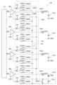
- FIG. 3 is a diagram showing an example of a circuit configuration of an output circuit including an intermediate potential supply section
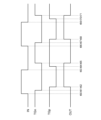
- 4 is a timing chart showing an example of potential transition of each signal in an output circuit
- FIG. 3 is a diagram showing a first example of a circuit configuration of a transmission driver
- FIG. 10 is a diagram showing a second example of the circuit configuration of a transmission driver
- FIG. 11 is a diagram showing a third example of the circuit configuration of a transmission driver
- FIG. 3 is a diagram showing part of the circuit configuration of an output circuit and an example of a touch sensor
- FIG. 3 is a diagram showing an example of a circuit configuration of an output circuit including an intermediate potential supply section
- 4 is a timing chart showing an example of potential transition of each signal in an output circuit
- FIG. 3 is a diagram showing a first example of a circuit configuration of a transmission driver
- FIG. 10 is a diagram showing a
- FIG. 12 is a diagram showing a fourth example of the circuit configuration of the transmission driver; 4 is a timing chart showing an example of potential transition of each signal in a transmission driver;
- FIG. 10 is a diagram showing an example of a circuit configuration of an output circuit including an intermediate potential supply section according to the second embodiment; 9 is a timing chart showing potential transition of each signal in the output circuit according to the second embodiment.
- FIG. 11 is a diagram showing an example of the circuit configuration of an output circuit including an intermediate potential supply section according to the third embodiment; 9 is a timing chart showing an example of potential transition of each signal in the output circuit according to the third embodiment. It is a diagram showing a first example of the circuit configuration of the output control circuit according to the third embodiment.
- FIG. 14 is a diagram showing an example of a circuit configuration of an output circuit including an intermediate potential supply section according to a fourth embodiment;
- FIG. 14 is a timing chart showing an example of potential transition of each signal in the output circuit according to the fourth embodiment;
- FIG. 3 is a diagram showing an example of a circuit configuration of a voltage source in a potential generator;
- FIG. 5 is a flow chart showing an example of a series of processing flows of the output circuit according to the first embodiment and the second embodiment;
- FIG. 11 is a flow chart showing an example of the flow of a series of operations of the output circuit according to the third embodiment and the fourth embodiment;
- this embodiment An embodiment of the present invention (hereinafter referred to as "this embodiment") will be described below with reference to the accompanying drawings.
- the same components and steps are denoted by the same reference numerals as much as possible in each drawing, and overlapping descriptions are omitted.
- FIG. 1 is a diagram showing an example of an electronic device 1 according to the first embodiment.
- the electronic device 1 is a computer owned by a user, and includes, for example, a tablet, a smart phone, a personal computer, and the like.
- a user can write pictures or characters on the electronic device 1 by holding the stylus 2 as a pen-shaped pointing device and moving the stylus 2 while pressing the pen tip against the touch surface of the electronic device 1 .
- the stylus 2 is, for example, an active electrostatic coupling (AES) electronic pen, and is configured to be able to communicate bidirectionally with the electronic device 1 .
- AES active electrostatic coupling
- the electronic device 1 detects the pointing position of the stylus 2 and performs various information processing according to the detection result. Specifically, the electronic device 1 transmits an uplink signal US to the stylus 2, detects the pointing position of the stylus 2 according to the reception result of the downlink signal DS from the stylus 2, and generates digital ink. processing and pointer display processing.
- the electronic device 1 includes a sensor controller 10 and a touch sensor 20 in addition to a host processor, memory, and communication module (none of which are shown).
- the touch sensor 20 is a capacitive sensor in which a plurality of detection electrodes are arranged in a plane.
- the touch sensor 20 includes, for example, a plurality of X-line electrodes (hereinafter referred to as "linear electrodes 21") for detecting the position of the X-axis of the sensor coordinate system, and a plurality of electrodes for detecting the position of the Y-axis.
- Y line electrodes hereinafter referred to as “linear electrodes 22"
- the linear electrodes 21 and 22 may be made of a transparent conductive material containing ITO (Indium Tin Oxide), or may be made of a wire mesh sensor.
- the touch sensor 20 may be a self-capacitance sensor in which block-shaped electrodes are arranged in a two-dimensional lattice instead of the above-described mutual capacitance sensor.
- the sensor controller 10 includes an MCU (Micro Controller Unit) 11, a control circuit 12, a transmission circuit 13, a reception circuit 14, an output circuit 15, a detection circuit 16, and selection circuits 17 and 18. be.
- MCU Micro Controller Unit
- the output circuit 15 selects one of the plurality of linear electrodes 22 or a plurality of electrodes adjacent to each other, and amplifies the input signal transmitted from the control circuit 12 to a predetermined voltage. It is a circuit for outputting the output signal to the linear electrode 22 as an output signal.
- the detection circuit 16 is a circuit that selects one of the plurality of linear electrodes 21 or a plurality of mutually adjacent linear electrodes 21 based on an instruction from the control circuit 12 .
- the selection circuit 17 is, for example, a multiplexer, and is a circuit for switching whether the linear electrodes 22 selected by the output circuit 15 are used for reception or for transmission.
- the selection circuit 17 connects the linear electrode 22 selected by the output circuit 15 to the reception circuit 14 via the selection circuit 18 when the selection signal SELY output from the control circuit 12 is in the low state "0".
- the selection circuit 17 supplies the input signal input from the control circuit 12 via the transmission circuit 13 to the linear electrode 22 selected by the output circuit 15 when the selection signal SELY is in the high state “1”.
- the selection circuit 18 is, for example, a multiplexer, and receives a signal input from the linear electrode 22 selected by the output circuit 15 via the selection circuit 17, or a signal input from the linear electrode 21 selected by the detection circuit 16. and outputs the selected signal to the receiving circuit 14 .
- the selection circuit 18 connects the linear electrode 22 selected by the output circuit 15 to the reception circuit 14 when the selection signal SELX output from the control circuit 12 is in the low state.
- the selection circuit 18 connects the linear electrode 22 selected by the output circuit 15 via the selection circuit 17 to the reception circuit 14 when the selection signal SELX is in a high state.
- the electronic device 1 has the following four types of modes, and the control circuit 12 controls each circuit in the sensor controller 10 while switching these modes in the following order. Each will be described in detail below.
- the first mode is a mode that detects the position of the finger.
- the control circuit 12 sets the selection signal SELY to a high state and the selection signal SELX to a low state. That is, the linear electrode 22 selected by the output circuit 15 is supplied with a transmission signal output from the control circuit 12 via the transmission circuit 13 and the output circuit 15, and the touch sensor 20 transmits a touch detection signal. Also, the linear electrodes 21 selected by the detection circuit 16 are connected to the reception circuit 14 .
- the MCU 11 reads the change in the detection signal due to the contact of the finger on the sensor surface and calculates the coordinate position of the finger.
- the second mode is a mode in which an uplink signal US is transmitted to the stylus 2.
- the control circuit 12 outputs a transmission signal to the linear electrode 22 selected by the output circuit 15 via the transmission circuit 13 and the output circuit 15 by setting the selection signal SELY to a high state. is supplied, and an uplink signal US is transmitted from the touch sensor 20 .
- the output circuit 15 may select an electrode in the vicinity of the linear electrode 22 pointed by the stylus 2 and transmit the uplink signal US, or the output circuit 15 may select all of the linear electrodes 22 . electrodes may be simultaneously selected to transmit the trigger signal US_trg.
- a third mode is a mode in which the position of the stylus 2 is detected by detecting the position signal DS_pos transmitted by the stylus 2 .
- the control circuit 12 sets the selection signal SELY to a low state so that the linear electrodes 22 selected by the output circuit 15 are connected to the reception circuit 14 via the selection circuit 17 .
- the control circuit 12 sets the selection signal SELX to the low state and connects the linear electrode 21 selected by the detection circuit 16 to the reception circuit 14 .
- the detection circuit 16 selects a plurality of linear electrodes 21 centering on the linear electrode 21 closest to the pointing position of the stylus 2, for example, five linear electrodes 21 one by one.
- the MCU 11 reads the data output from the receiving circuit 14 as a signal level value.
- the MCU 11 calculates the X-axis coordinates of the stylus 2 from the signal level distribution for the selected linear electrodes 21 .
- the control circuit 12 sets the selection signal SELX to a high state and connects the linear electrode 22 selected by the output circuit 15 to the reception circuit 14 .
- the linear electrodes 22 selected by the output circuit 15 are sequentially selected one by one from a plurality of linear electrodes 22 centering on the linear electrode 22 closest to the pointing position of the stylus 2, for example five linear electrodes 22.
- the MCU 11 reads the data output from the receiving circuit 14 as a signal level value.
- the MCU 11 calculates the Y-axis coordinates of the stylus 2 from the signal level distribution for the selected linear electrodes 22 .
- a fourth mode is a mode for receiving the data signal DS_res transmitted by the stylus 2 .
- the control circuit 12 connects the linear electrode 21 selected by the detection circuit 16 to the reception circuit 14 by setting the selection signal SELX to a low state. Further, the control circuit 12 is operated so that the detection circuit 16 simultaneously selects a plurality of, for example, three linear electrodes 21 centering on the linear electrode 21 closest to the pointed position of the stylus 2 . In this state, MCU 11 periodically reads the output from receiving circuit 14 .
- the selection signal SELY should be set to the low state and the selection signal SELX should be set to the high state.
- control circuit 12 is configured to transmit and receive signals using the same touch sensor 20 for transmission and reception.
- Other configurations in the electronic device 1 shown in FIG. 1 will be described below.
- the MCU 11 is a microprocessor that has ROM (Read Only Memory) and RAM (Random Access Memory) inside and operates based on a predetermined program, and outputs each signal output from the control circuit 12 as described above. It controls the control circuit 12 as described above, and reads and processes the digital data output from the receiving circuit 14 .
- ROM Read Only Memory
- RAM Random Access Memory
- the control circuit 12 is a logic circuit for accurately outputting each signal at designated timing based on instructions from the MCU 11 .
- FIG. 2 is a diagram showing part of the circuit configuration of the output circuit 15 and an example of the touch sensor 20 according to this embodiment.
- the output circuit 15 includes a driver selection circuit 151, a plurality of transmission drivers 152, and an intermediate potential supply section 153.
- a driver selection circuit 151 selects some of a plurality of transmission drivers 152 that transmit signals to the linear electrodes 22 according to instructions from the control circuit 12, and uses data signals transmitted from the transmission circuit 13 as a plurality of input signals IN. , outputs each input signal IN to the corresponding transmission driver 152 .
- One transmission driver 152 is provided for one linear electrode 22 .
- the transmission driver 152 amplifies the input signal IN input from the driver selection circuit 151 to a potential difference that allows the signal to be transmitted from the linear electrodes 22, and outputs the amplified signal as the transmission signal OUT to the output signal line Wout. to the corresponding linear electrode 22.
- the potential difference with which a signal can be transmitted from the linear electrode 22 is 5 V, which is a potential of, for example, 0 V (first potential) at the low level and a potential of about 9 V (second potential) at a high level of 5 V or higher.
- the potential difference is about 9V.
- the transmission driver 152 also has a positive power supply terminal to which a positive power supply potential (high level) is supplied and a negative power supply terminal to which a negative power supply potential (low level) is supplied.
- the intermediate potential supply section 153 generates an intermediate potential that is a potential between high level and low level.
- the intermediate potential is, for example, a potential obtained by adding the values of the high level and the low level and dividing the result by two.
- the intermediate potential supply unit 153 generates an intermediate potential at the positive power supply terminal of the transmission driver 152 selected by the driver selection circuit 151 at the timing when the potential of the signal waveform generated by the transmission driver 152 transitions from low level to high level. supply.
- the intermediate potential supply unit 153 generates an intermediate potential at the negative power supply terminal of the transmission driver 152 selected by the driver selection circuit 151 at the timing when the potential of the signal waveform generated by the transmission driver 152 transitions from high level to low level. supply.
- the intermediate potential supply unit 153 stops supplying the intermediate potential to the transmission driver 152 at the timing when the potential of the signal waveform generated by the transmission driver 152 to which the intermediate potential is supplied reaches the intermediate potential.
- FIG. 3 is a diagram showing an example of the circuit configuration of the output circuit 15 including the intermediate potential supply section 153A according to this embodiment.
- the output circuit 15A includes a driver selection circuit 151, a plurality of transmission drivers 152A, and an intermediate potential supply section 153A.
- the driver selection circuit 151 selects n+1 transmission drivers 152A.
- n is a positive integer.
- the linear electrode 22 has a capacitive element Cout as a load capacitance.
- the capacitance of the capacitive element Cout is, for example, approximately 1200 pF.
- the driver selection circuit 151 selects n+1 transmission drivers 152A and transmits the input signal IN to the selected transmission drivers 152A.
- the input signal IN0 is input to the 0th transmission driver 152A.
- An input signal IN1 is input to the first transmission driver 152A, an input signal INn-1 is input to the nth transmission driver 152A, and an input signal INn is input to the n+1th transmission driver 152A.
- the transmission driver 152A is a driver with an output control function added to the transmission driver 152 described above.
- the transmission driver 152A sets the mode to the output mode or the stop mode according to the output control signal EN output from the control circuit 12.
- FIG. On the other hand, in the output mode, the transmission driver 152A amplifies the input signal IN to a potential difference that allows the signal to be transmitted from the linear electrode 22, and outputs the amplified signal as the transmission signal OUT through the output signal line Wout. to transmit the transmission signal OUT to the corresponding linear electrode 22 .
- the transmission driver 152A sets the output state to the high impedance state "Hi-Z" and stops the transmission of the transmission signal OUT.
- the intermediate potential supply section 153A includes a potential generation section 154A, a plurality of short circuit control elements SWU, a plurality of short circuit control elements SWD, a short circuit control element SWr, a reset voltage source Vrst, and a short circuit signal line Ws. Configured.
- the potential generator 154A is configured including, for example, a voltage source Vmid and a capacitive element Cext.
- the voltage source Vmid is, for example, a voltage source that generates an intermediate potential.
- the potential generator 154A generates an intermediate potential, for example, 4.5 V, and applies the generated intermediate potential to the short-circuit signal line Ws.
- the capacitive element Cext is, for example, a capacitor with a capacitance of approximately 1 uF, one end of which is connected to the short-circuit signal line Ws, and the other end of which is connected to the reference line GND.
- the capacitive element Cext charges or discharges electric charges according to the potential supplied to the short-circuit signal line Ws, thereby stabilizing the potential of the short-circuit signal line Ws.
- the potential generator 154A includes the voltage source Vmid and the capacitive element Cext, but may be configured with only one of the voltage source Vmid and the capacitive element Cext.
- the reset voltage source Vrst is a voltage source that generates an initial potential (eg, 4.5 V), and supplies the initial potential generated when the short-circuit control element SWr is short-circuited to the short-circuit signal line Ws.
- the reset voltage source Vrst has one end connected to the other end of the short-circuit control element SWr and the other end connected to the reference line GND.
- the short-circuit control elements SWU, SWD, and SWr are, for example, switch elements, transistors, and the like.
- the short-circuit control elements SWU, SWD, and SWr short-circuit or open both ends according to the input signal.
- the short-circuit control elements SWU, SWD, and SWr short-circuit both ends when the state of the input signal is high.
- the short-circuit control elements SWU, SWD, and SWr open both ends when the state of the input signal is low.
- the short circuit control elements SWU and SWD are provided for each transmission driver 152A.
- the short-circuit control element SWr has one end connected to the short-circuit signal line Ws and the other end connected to one end of the reset voltage source Vrst.
- the short-circuit control element SWr short-circuits or opens both ends according to the reset signal RST output from the control circuit 12 .
- the short-circuit control element SWU has one end connected to the corresponding positive power supply terminal of the transmission driver 152A, and the other end connected to the short-circuit signal line Ws.
- the short-circuit control element SWU short-circuits or opens both ends according to a control signal CTU output from the control circuit 12 .
- the short-circuit control element SWD has one end connected to the negative power supply terminal of the corresponding transmission driver 152A, and the other end connected to the short-circuit signal line Ws.
- the short-circuit control element SWD short-circuits or opens both ends according to the control signal CTD output from the control circuit 12 .
- the control circuit 12 controls the state of the transmission driver 152A to the high impedance state at the timing when any one of the input signals IN0 to INn transitions from the low state to the high state.
- the short circuit control element SWU is controlled to be in a short circuit state.
- the control circuit 12 controls the state of the transmission driver 152A to the high impedance state at the timing when the state of any one of the input signals IN0 to INn transitions from the high state to the low state, and the short circuit control element SWD is set to the short circuit state. to control.
- the positive power supply terminal of the transmission driver 152A and the short-circuit signal line Ws corresponding to the input signal IN whose state transitions from the low state to the high state are short-circuited, and the state corresponds to the input signal IN whose state transitions from the high state to the low state. Since the negative power supply terminal of the transmission driver 152A and the short-circuit signal line Ws are short-circuited, the output signal line Wout with a high-level potential is connected to the output signal line Wout with a low-level potential through the short-circuit signal line Ws and the capacitive element A potential is supplied to Cext. Further, a potential is supplied from the voltage source Vmid and the capacitive element Cext to the output signal line Wout whose potential is at a low level through the short-circuit signal line Ws.
- the control circuit 12 changes the state of the transmission driver 152A to the output state at the timing when the potentials of the positive power supply terminal, the negative power supply terminal, the short-circuit signal line Ws, and one end of the capacitive element Cext of each transmission driver 152A reach the intermediate potential. , and the short circuit control elements SWU and SWD are controlled to be in an open state.
- the potential of each output signal line Wout transitions to a high level or a low level by the corresponding transmission driver 152A, and transmission signals OUT0, OUT1, OUTn ⁇ 1 and OUTn are transmitted via the linear electrodes 22.
- FIG. 5A is a diagram showing an example of the circuit configuration of the transmission driver 152A according to this embodiment.
- the transmission driver 152A includes, for example, logic NOT circuits INV1 and INV2, transistors TR1, TR2, TR3 and TR4, a power supply line VDD, and a reference line GND.
- the logical NOT circuits INV1 and INV2 are, for example, inverter circuits including transistors.
- the logical NOT circuit INV1 performs a logical NOT operation on the input signal IN input from the driver selection circuit 151, and outputs the signal resulting from the operation to the gate terminals of the transistors TR2 and TR3.
- the logical NOT circuit INV2 performs a logical NOT operation on the output control signal EN input from the control circuit 12, and outputs the signal resulting from the operation to the gate terminal of the transistor TR1.
- the transistors TR1 and TR2 are, for example, P-type MOS (Metal Oxide Semiconductor) transistors.
- the transistors TR1 and TR2 supply or stop the supply of the potential supplied to the source terminal to the drain terminal according to the signal input to the gate terminal. Specifically, when the state of the signal input to the gate terminal is low, the transistors TR1 and TR2 supply the potential supplied to the source terminal to the drain terminal, while the potential of the signal input to the gate terminal is low. If the state is high, stop the supply.
- the transistor TR1 has a gate terminal connected to the output terminal of the logical NOT circuit INV2, a source terminal connected to the power supply line VDD, and a drain terminal connected to the positive power supply terminal of the transmission driver 152A.
- the transistor TR2 has a gate terminal connected to the output terminal of the logical NOT circuit INV1, a source terminal connected to the positive power supply terminal of the transmission driver 152A, and a drain terminal connected to the drain terminal of the transistor TR3 and the output signal line Wout.
- the transistors TR3 and TR4 are, for example, N-type MOS (Metal Oxide Semiconductor) transistors.
- the transistors TR3 and TR4 extract or stop extracting charges from the drain terminal to the source terminal according to the signal input to the gate terminal. Specifically, when the state of the signal input to the gate terminal of the transistors TR3 and TR4 is high, the transistors TR3 and TR4 extract charge from the drain terminal toward the source terminal, while the state of the signal input to the gate terminal is high. If it is in the low state, it stops the extraction.
- N-type MOS Metal Oxide Semiconductor
- the transistor TR3 has a gate terminal connected to the output terminal of the logic NOT circuit INV1, a source terminal connected to the negative power supply terminal of the transmission driver 152A, and a drain terminal connected to the drain terminal of the transistor TR2 and the output signal line Wout.
- the transistor TR4 has a gate terminal connected to the control circuit 12, a source terminal connected to the reference line GND, and a drain terminal connected to the negative power supply terminal of the transmission driver 152A.
- a power supply line VDD supplies a high-level potential supplied from a voltage source (not shown) to the transmission driver 152A.
- the high-level potential is a potential of, for example, about 9V, which is 5V or higher.
- the reference line GND supplies a low-level potential to the transmission driver 152A.
- the low-level potential is, for example, a potential of 0V.
- the transmission driver 152A configured as described above amplifies the input signal IN to a potential difference at which the signal can be transmitted from the linear electrode 22. The amplified signal is transmitted to the output signal line Wout as the transmission signal OUT.
- the transmission driver 152A sets the output state to the high impedance state "Hi-Z" and stops the transmission of the transmission signal OUT.
- FIG. 5B is a diagram showing another example of the circuit configuration of the transmission driver 152 according to this embodiment.
- the transmission driver 152B includes, for example, current sources I0 and I1 in addition to the configuration of the transmission driver 152A described above.
- the description of the circuit configuration of the transmission driver 152B the description of the configuration similar to that of the transmission driver 152A is omitted.
- the current sources I0 and I1 are, for example, current mirror circuits including MOS transistors.
- the current source I0 limits the current flowing from the power supply line VDD toward the source terminal of the transistor TR1 to a constant current value.
- the current source I1 limits the current flowing from the source terminal of the transistor TR4 toward the reference line GND to a constant current value.
- the transmission driver 152B configured as described above limits the current flowing from the power supply line VDD to the transmission driver 152B and the current flowing from the transmission driver 152B to the reference line GND to a constant current value, thereby increasing the potential of the transmission signal OUT. transition as compared to transmit driver 152A. As a result, the EMI characteristics of the transmission driver 152B are improved compared to the transmission driver 152A by reducing the high frequency components of the transmission driver 152B.
- FIG. 5C is a diagram showing another example of the circuit configuration of the transmission driver 152 according to this embodiment.
- the transmission driver 152C includes, for example, an OR circuit OR, an AND circuit AND, and delay circuits DL0 and DL1 in addition to the configuration of the transmission driver 152A described above.
- the description of the circuit configuration of the transmission driver 152C the description of the configuration similar to that of the transmission driver 152A is omitted.
- the logical sum circuit OR includes, for example, a MOS transistor, performs a logical sum operation on the output signal of the logical NOT circuit INV1 and the trigger signal TGn output from the delay circuit DL1, and delays the result of the operation. Output to circuit DL0.
- the logical product circuit AND which includes, for example, a MOS transistor, performs a logical product operation on the output signal of the logical NOT circuit INV1 and the trigger signal TGp output from the delay circuit DL0, and delays the result of the operation. Output to circuit DL1.
- the delay circuits DL0 and DL1 are buffer circuits including, for example, MOS transistors.
- the delay circuit DL0 delays the output signal of the OR circuit OR by the delay time td, and outputs the delayed signal as the trigger signal TGp to the gate terminal of the transistor TR2 and the AND circuit AND.
- the delay circuit DL1 delays the output signal of the AND circuit AND by the delay time td, and outputs the delayed signal as the trigger signal TGn to the gate terminal of the transistor TR3 and the OR circuit OR.
- the OR circuit OR, the AND circuit AND, the drain terminal and the source terminal of the transistor TR2, and the drain terminal and the source terminal of the transistor TR3 are simultaneously conductive. Therefore, it is possible to prevent a through current from occurring from the power supply line VDD to the reference line GND via the transistors TR1 to TR4.
- FIG. 6 is a timing chart showing the potential transition of each signal in the transmission driver 152C according to this embodiment. Although not shown, the state of the output control signal EN is assumed to be high level at any time.
- the driver selection circuit 151 changes the state of the input signal IN from low to high.
- the logical NOT circuit INV1 performs a logical NOT operation on the input signal IN (high state), and outputs a low state signal as a result of the operation to the OR circuit OR and AND circuit AND.
- the logical product circuit AND performs a logical product operation on the trigger signal TGp (high state) and the signal (low state) output from the logical NOT circuit INV1, and the signal that has become low as a result of the operation is is output to the delay circuit DL1.
- the delay circuit DL1 receives the low-state signal from the AND circuit AND and delays the signal by the delay time td.
- the delay circuit DL1 outputs the delayed result as the trigger signal TGn, and outputs the low-state trigger signal TGn to the gate terminal of the transistor TR3 and the OR circuit OR.
- the transistor TR3 receives the low-state trigger signal TGn and makes the drain terminal and the source terminal non-conductive. As a result, both the drain terminal and the source terminal of the transistor TR2 and the drain terminal and the source terminal of the transistor TR3 are disconnected, so that the state of the output signal line Wout becomes a high impedance state.
- the OR circuit OR performs a logical sum operation on the trigger signal TGn (low state) and the signal (low state) output from the logic NOT circuit INV1, and the signal that has become low as a result of the operation is is output to the delay circuit DL0.
- the delay circuit DL0 receives the low state signal from the OR circuit OR and delays the signal by the delay time td.
- the delay circuit DL0 uses the delayed result as the trigger signal TGp and outputs the low-state trigger signal TGp to the gate terminal of the transistor TR2 and the AND circuit AND.
- the transistor TR2 receives the low-state trigger signal TGp, and conducts between the drain terminal and the source terminal. As a result, a high level potential is supplied from the power supply line VDD to the output signal line Wout via the transistors TR1 and TR2, and the potential of the transmission signal OUT transitions to a high level.
- the driver selection circuit 151 changes the state of the input signal IN from high to low.
- the logical NOT circuit INV1 performs a logical NOT operation on the input signal IN (low state), and outputs a high state signal as a result of the operation to the OR circuit OR and AND circuit AND.
- the OR circuit OR performs a logical sum operation on the trigger signal TGn (low state) and the signal (high state) output from the logical NOT circuit INV1, and the signal that has become high as a result of the operation is is output to the delay circuit DL0.
- the delay circuit DL0 receives the high-state signal from the OR circuit OR and delays the signal by the delay time td.
- the delay circuit DL0 uses the delayed result as the trigger signal TGp and outputs the high-state trigger signal TGp to the gate terminal of the transistor TR2 and the AND circuit AND.
- the transistor TR2 receives the high-state trigger signal TGp, and renders the drain terminal and the source terminal non-conductive. As a result, both the drain terminal and the source terminal of the transistor TR2 and the drain terminal and the source terminal of the transistor TR3 are disconnected, so that the state of the output signal line Wout becomes a high impedance state.
- the logical product circuit AND performs a logical product operation on the trigger signal TGp (high state) and the signal (high state) output from the logical NOT circuit INV1, and outputs a high state signal as a result of the operation. is output to the delay circuit DL1.
- delay circuit DL1 receives the signal in the high state from AND circuit AND and delays the signal by delay time td.
- the delay circuit DL1 uses the delayed result as the trigger signal TGn and outputs the high-state trigger signal TGn to the gate terminal of the transistor TR3 and the OR circuit OR.
- the transistor TR3 receives the trigger signal TGn in the high state and conducts between the drain terminal and the source terminal. As a result, charges are extracted from the output signal line Wout toward the reference line GND via the transistors TR1 and TR2, and the potential of the transmission signal OUT transitions to low level.
- FIG. 5D is a diagram showing another example of the circuit configuration of the transmission driver 152 according to the first embodiment of the invention.
- the transmission driver 152D has a configuration in which the configuration of the transmission driver 152C is added to the configuration of the transmission driver 152B described above. Therefore, description of the circuit configuration of the transmission driver 152D is omitted.
- the transmission driver 152D is configured by combining the configurations of the transmission drivers 152B and 152C, the EMI characteristics are improved compared to the transmission driver 152A by reducing the high frequency component, and It is possible to prevent the generation of through current from the power supply line VDD to the reference line GND via the transistors TR1 to TR4.
- FIG. 4 is a timing chart showing potential transition of each signal in the output circuit 15A according to the present embodiment.
- the control circuit 12 opens both ends of the short circuit control element SWr by setting the state of the reset signal RST to the low state. As a result, the supply of the initial potential from the reset voltage source Vrst to the short-circuit signal line Ws is stopped.
- the driver selection circuit 151 causes the states of the input signals IN0 and INn ⁇ 1 to transition from the low state to the high state, and causes the states of the input signals IN1 and INn to transition from the high state to the low state.
- Input signals IN0, IN1, INn-1 and INn are applied to corresponding transmit drivers 152A.
- the control circuit 12 changes the state of the output control signal EN from the high state to the low state, and sets the mode of each transmission driver 152A to the stop mode. Also, at time t41, the control circuit 12 transitions the states of the control signals CTU0, CTUn-1, CTD1 and CTDn from the low state to the high state, and short-circuits the control signals CTU0, CTUn-1, CTD1 and CTDn correspondingly. By outputting to the control element SWU or SWD, both ends of each short control element SWU and SWD are short-circuited.
- the output signal lines Wout are short-circuited via the short-circuit control elements SWU and SWD whose both ends are short-circuited.
- charges are supplied from the output signal line Wout with a high level potential and the output signal line Wout with a low level potential from the potential generator 154A, whereby the transmission signals OUT0, OUT1, OUTn-1 and OUTn are changed.
- the potential becomes an intermediate potential.
- the control circuit 12 causes the state of the output control signal EN to transition from the low state to the high state, and sets the mode of each transmission driver 152A to the output mode.
- the control circuit 12 causes the states of the control signals CTU0, CTUn-1, CTD1 and CTDn to transition from the high state to the low state, and converts the control signals CTU0, CTUn-1, CTD1 and CTDn to the respective short circuit control elements.
- SWU or SWD both ends of each short control element SWU or SWD are opened.
- the short-circuit state between the output signal lines Wout is released.
- the electric charges are supplied from the corresponding transmission driver 152A, so that the electric potentials of the transmission signals OUT0 and OUTn-1 transition from the intermediate electric potential to the high level, while electric charges are extracted from the corresponding transmission driver 152A.
- the potentials of the transmission signals OUT1 and OUTn transition from the intermediate potential to the low level.
- the control circuit 12 changes the state of the output control signal EN from the high state to the low state, and sets the mode of each transmission driver 152A to the stop mode. Also, at time t43, the control circuit 12 causes the states of the control signals CTD0, CTDn-1, CTU1 and CTUn to transition from the low state to the high state, and controls the control signals CTD0, CTDn-1, CTU1 and CTUn to the corresponding short-circuit control. By outputting to the element SWU or SWD, both ends of each short control element SWU and SWD are opened. As a result, at time t43, the potentials of the transmission signals OUT0, OUT1, OUTn-1, and OUTn become intermediate potentials, as at time t41.
- the control circuit 12 causes the state of the output control signal EN to transition from the low state to the high state, and sets the mode of each transmission driver 152A to the output mode. Also, at time t44, the control circuit 12 causes the states of the control signals CTD0, CTDn-1, CTU1 and CTUn to transition from the high state to the low state, and controls the control signals CTD0, CTDn-1, CTU1 and CTUn to the corresponding short-circuit control. By outputting to the element SWU or SWD, both ends of each short control element SWU and SWD are opened. As a result, at time t44, the short-circuit state between the output signal lines Wout is released.
- the potentials of the transmission signals OUT0 and OUTn-1 transition from the intermediate potential to the low level due to the supply of charges from the corresponding transmission driver 152A.
- the potentials of the transmission signals OUT1 and OUTn transition from the intermediate potential to the high level.
- FIG. 15 is a flow chart showing a series of processes of the output circuit 15A according to the first embodiment.
- Step SP20 The transmission driver 152A amplifies the input signal IN input from the driver selection circuit 151 to a potential difference that allows the signal to be transmitted from the linear electrode 22, and converts the amplified signal into the transmission signal OUT. It transmits to the corresponding output signal line Wout. Then, the process shifts to the process of step SP12.
- Step SP22 The control circuit 12 determines whether the signal waveform of the transmission signal OUT rises from low level to high level. On the other hand, if the determination is affirmative, the process proceeds to step SP24. On the other hand, if the determination is negative, the process proceeds to step SP32.
- Step SP24 The control circuit 12 sets the mode of the transmission driver 152A to the stop mode. As a result, the state of the output of the transmission driver 152A becomes a high impedance state. Then, the process shifts to the process of step SP26.
- Step SP26 The control circuit 12 controls to short-circuit both ends of each short-circuit control element SWU.
- the output signal lines Wout are short-circuited to each other via the short-circuit signal line Ws, and from the potential generator 154A and the output signal line Wout whose potential is high level, via the short-circuit signal line Ws, the potential is low.
- a potential is supplied to a certain output signal line Wout.
- the potentials of the short-circuit signal line Ws and each output signal line Wout become intermediate potentials. Then, the process shifts to the process of step SP28.
- the control circuit 12 determines which short-circuit signal line Ws each output signal line Wout is to be connected to.
- the short-circuit control element SWU corresponding to the signal line Ws is controlled to be short-circuited.
- Step SP28 The control circuit 12 controls to open both ends of each short circuit control element SWU. As a result, the short circuit between the output signal lines Wout is released. Then, the process shifts to the process of step SP30.
- Step SP30 The control circuit 12 sets the mode of the transmission driver 152A to the output mode. As a result, a high level is supplied from the transmission driver 152A to the output signal line Wout.
- the potential of the transmission signal OUT transitions from an intermediate potential to a high level according to the potential of the output signal line Wout.
- Step SP32 The control circuit 12 determines whether the signal waveform of the transmission signal OUT falls from high level to low level. On the other hand, if the determination is affirmative, the process proceeds to step SP34. On the other hand, if the determination is negative, the process ends the series of processes according to FIG.
- Step SP34 The control circuit 12 sets the mode of the transmission driver 152A to the stop mode. As a result, the state of the output of the transmission driver 152A becomes a high impedance state. Then, the process shifts to the process of step SP36.
- Step SP36 The control circuit 12 controls to short-circuit both ends of each short-circuit control element SWD.
- the output signal lines Wout are short-circuited to each other via the short-circuit signal line Ws, and from the potential generator 154A and the output signal line Wout whose potential is high level, via the short-circuit signal line Ws, the potential is low.
- a potential is supplied to a certain output signal line Wout.
- the potentials of the short-circuit signal line Ws and each output signal line Wout become intermediate potentials. Then, the process shifts to the process of step SP38.
- the control circuit 12 determines which short-circuit signal line Ws each output signal line Wout is to be connected to.
- the short-circuit control element SWD corresponding to the signal line Ws is controlled to be short-circuited.
- Step SP38 The control circuit 12 controls to open both ends of each short circuit control element SWD. As a result, the short circuit between the output signal lines Wout is released. Then, the process shifts to the process of step SP40.
- Step SP40 The control circuit 12 sets the mode of the transmission driver 152A to the output mode. As a result, a low level is supplied from the transmission driver 152A to the output signal line Wout. The potential of the transmission signal OUT transitions from the intermediate potential to the low level according to the potential of the output signal line Wout.
- the sensor controller 10 is connected to the touch sensor 20 in which the plurality of linear electrodes 21 and 22 are arranged in a plane.
- the sensor controller 10 has a positive power supply terminal and a negative power supply terminal, a first potential (low level) supplied to the negative power supply terminal, and a second potential (low level) supplied to the positive power supply terminal, which is higher than the first potential.
- a plurality of transmission drivers 152A that generate signal waveforms that transition between the potential (high level) of and output to the corresponding linear electrodes 22 as transmission signals; It has a potential generator 154A including Cext, and the potential of the signal waveform transitions from the first potential (low level) to the second potential (high level) or from the second potential (high level) to the first potential ( At the first timing (times t41, t43, t45, and t47) to start the transition to low level), the voltage is output from the potential generation unit 154A so that the first potential (low level) and the second potential (high level) are output. level) to at least one of the positive power supply terminal and the negative power supply terminal.
- the sensor controller 10 supplies voltage from the intermediate potential supply unit 153A having the potential generation unit 154A having the voltage source Vmid or the capacitive element Cext separate from the transmission driver 152A to the positive power supply terminal and the negative power supply terminal of the transmission driver 152A.
- the sensor controller 10 can reduce power consumption without connecting an element such as a switch to the output signal line Wout as compared with the conventional configuration.
- the output side of the potential generator 154A is connected to two or more of the plurality of transmission drivers 152A.
- the sensor controller 10 can suppress through current and reduce power consumption compared to the conventional configuration.
- the sensor controller 10 includes a control circuit 12 that transmits control signals CTU and CTD.
- the transmission driver 152A has an output mode for outputting a transmission signal OUT, a second potential (high level) supply from the power supply line VDD to the positive power supply terminal, and a first potential (high level) supply from the reference line GND to the negative power supply terminal. and a stop mode in which the supply of the potential (low level) is stopped and the state of the output is changed to a high impedance state.
- control circuit 12 controls the transmission driver 152A to enter the stop mode at the first timing, and at the second timings (times t42, t44, t46 and t48) after a predetermined time has elapsed from the first timing. ) to set the transmission driver 152A to the output mode.
- the sensor controller 10 sets the state of the output of each transmission driver 152A to the high impedance state, and provides a period for stably supplying the intermediate potential from the intermediate potential supply unit 153A to each transmission driver 152A.
- power consumption can be reduced.
- the intermediate potential supply section 153A has both ends shorted or opened according to the control signal CTU, one end connected to the corresponding positive power supply terminal, and the other end connected to the output side of the potential generation section 154A.
- a plurality of first short-circuit control elements SWU and a plurality of first short-circuit control elements SWU having both ends shorted or opened according to a control signal CTD, one end connected to a corresponding negative power supply terminal, and the other end connected to the output side of the potential generating section 154A. and two short circuit control elements SWD.
- control circuit 12 controls at least one of the first short-circuit control element SWU and the second short-circuit control element SWD to short-circuit at the first timing, and the first short-circuit control element SWU and the second short-circuit control element SWD short-circuited at the first timing. At least one of the short circuit control element SWU and the second short circuit control element SWD is controlled to be opened at the second timing.
- the sensor controller 10 can reduce power consumption compared to the conventional configuration without connecting elements such as switches to the output signal line Wout.
- control circuit 12 controls the first potential (low level) to the second potential (high level) at the timing when the potential of the signal waveform starts to transition from the first potential (low level) to the second potential (high level).
- short-circuit control element SWU, and the second short-circuit control is performed at the timing when the potential of the signal waveform starts transitioning from the second potential (high level) to the first potential (low level) in the first timing Short the element SWD.
- the sensor controller 10 can reduce power consumption compared to the conventional configuration without connecting elements such as switches to the output signal line Wout.
- the second potential (high level) is a potential of 5 V or higher, and the second potential (high level) is a potential higher than the first potential (low level).
- the sensor controller 10 can reduce power consumption even when using the transmission driver 152A driven at a voltage of 5V or higher.
- FIG. 7 is a diagram showing an example of a circuit configuration of an output circuit 15B including an intermediate potential supply section 153B according to the second embodiment.
- the output circuit 15B includes a driver selection circuit 151, a plurality of transmission drivers 152A, and an intermediate potential supply section 153B.
- the driver selection circuit 151 selects n+1 transmission drivers 152A.
- the linear electrode 22 has a capacitive element Cout as a load capacitance.
- the capacitance of the capacitive element Cout is, for example, approximately 1200 pF.
- the driver selection circuit 151 and the transmission driver 152A are the same as those described in the first embodiment, so description thereof will be omitted.
- the intermediate potential supply section 153B includes a potential generation section 154B, a plurality of short control elements SWU and SWD, short circuit signal lines Wsu and Wsd, a short circuit control element SWr, and a capacitive element Cext.
- the potential generator 154B is configured including, for example, a capacitive element Cext.
- the capacitive element Cext is, for example, a capacitor having a capacitance of approximately 1 uF, one end of which is connected to the short-circuit signal line Wsu, and the other end of which is connected to the short-circuit signal line Wsd.
- the capacitive element Cext charges or discharges according to the potential difference between the potentials supplied to the short-circuit signal lines Wsu and Wsd, thereby stabilizing the potentials of the short-circuit signal lines Wsu and Wsd.
- the short circuit control elements SWUU, SWUD, SWDU, SWDD and SWr are, for example, switching elements and transistors.
- the short-circuit control elements SWUU, SWUD, SWDU, SWDD and SWr short-circuit or open both ends according to the input signal.
- the short-circuit control elements SWUU, SWUD, SWDU, SWDD, and SWr short-circuit both ends when the state of the input signal is high.
- the short circuit control elements SWUU, SWUD, SWDU, SWDD and SWr open both ends when the state of the input signal is low.
- Short circuit control elements SWUU, SWUD, SWDU, and SWDD are provided for each transmission driver 152A.
- the short-circuit control element SWr short-circuits or opens the short-circuit signal line Ws and the reset voltage source Vrst according to the reset signal RST output from the control circuit 12 .
- the short-circuit control element SWr has one end connected to the short-circuit signal line Wsu and the other end connected to one end of the short-circuit signal line Wsd.
- the short-circuit control element SWr short-circuits the short-circuit signal lines Wsu and Wds when short-circuited, and releases the short-circuit of the short-circuit signal lines Wsu and Wds when opened.
- the short-circuit control element SWUU has one end connected to the positive power supply terminal of the corresponding transmission driver 152A, and the other end connected to the short-circuit signal line Wsu.
- the short-circuit control element SWUU short-circuits or opens both ends according to a control signal CTUU output from the control circuit 12 to each short-circuit control element SWUU.
- the short-circuit control element SWUD has one end connected to the positive power supply terminal of the corresponding transmission driver 152A, and the other end connected to the short-circuit signal line Wsd.
- the short-circuit control element SWUD short-circuits or opens both ends according to a control signal CTUD output from the control circuit 12 to each short-circuit control element SWUD.
- the short-circuit control element SWDU has one end connected to the negative power supply terminal of the corresponding transmission driver 152 and the other end connected to the short-circuit signal line Wsu.
- the short-circuit control element SWDU short-circuits or opens both ends according to a control signal CTDU output from the control circuit 12 to each short-circuit control element SWDU.
- the short-circuit control element SWDD has one end connected to the negative power supply terminal of the corresponding transmission driver 152 and the other end connected to the short-circuit signal line Wsd.
- the short-circuit control element SWDD short-circuits or opens both ends according to a control signal CTDD output from the control circuit 12 for each short-circuit control element SWDD.
- the control circuit 12 operates at the timing when any one of the input signals IN0 to INn transitions from the high state to the low state, or at the timing when the state changes from the low state to the high state. , controls the state of the transmission driver 152A to a high impedance state.
- the control circuit 12 also assigns a value according to a code (for example, an orthogonal code) to each transmission driver 152A, and determines to which of the short-circuit signal lines Wsu and Wsd the corresponding transmission driver 152A is connected.
- a code for example, an orthogonal code
- the control circuit 12 determines to connect the transmission driver 152A to the short-circuit signal line Wsu.
- the value of the orthogonal code corresponding to a transmission driver 152A is "1”
- the control circuit 12 short-circuits the short-circuit control element SWUU corresponding to the transmission driver 152A determined to be connected to the short-circuit signal line Wsu at the timing when any one of the input signals IN0 to INn transitions from the low state to the high state.
- the short circuit control element SWDU corresponding to the transmission driver 152A determined to be connected to the short circuit signal line Wsd is controlled to be in the short circuit state.
- the control circuit 12 short-circuits the short-circuit control element SWUD corresponding to the transmission driver 152A determined to be connected to the short-circuit signal line Wsu at the timing when any of the input signals IN0 to INn transitions from the high state to the low state.
- the short circuit control element SWDD corresponding to the transmission driver 152A determined to be connected to the short circuit signal line Wsd is controlled to be in the short circuit state. Therefore, the output signal line Wout corresponding to the transmission driver 152A determined to be connected to the short-circuit signal line Wsu corresponds to one end of the capacitive element Cext via the short-circuit signal line Wsu and the transmission driver 152A determined to be connected to the short-circuit signal line Wsd. The output signal line Wout is short-circuited to the other end of the capacitive element Cext via the short-circuit signal line Wsd.
- the control circuit 12 controls the state of the transmission driver 152A to the output state at the timing when the potentials of each of the output signal lines Wout, the short-circuit signal lines Wsu and Wsd, and both ends of the capacitive element Cext reach an intermediate potential.
- the short circuit control elements SWUU, SWUD, SWDU and SWDD are controlled to be open.
- the potential of each output signal line Wout transitions to a high level or a low level by the corresponding transmission driver 152A, and transmission signals OUT0, OUT1, OUTn ⁇ 1 and OUTn are transmitted via the linear electrodes 22.
- FIG. 8 is a timing chart showing potential transition of each signal in the output circuit 15B according to the second embodiment.
- the control circuit 12 connects the transmission driver 152A corresponding to the transmission signals OUT0 and OUTn ⁇ 1 to the short-circuit signal line Wsu, and connects the transmission driver 152A corresponding to the transmission signals OUT1 and OUTn to the short-circuit signal line Wsd. shall decide to connect.
- the control circuit 12 opens both ends of the short circuit control element SWr by setting the state of the reset signal RST to the low state. As a result, the short-circuit state between the short-circuit signal lines Wsu and Wsd is released.
- the driver selection circuit 151 causes the states of the input signals IN0 and INn ⁇ 1 to transition from the low state to the high state, and causes the states of the input signals IN1 and INn to transition from the high state to the low state.
- Input signals IN0, IN1, INn-1 and INn are applied to corresponding transmit drivers 152A.
- the control circuit 12 changes the state of the output control signal EN from the high state to the low state, and sets the mode of each transmission driver 152A to the stop mode.
- the control circuit 12 causes the states of the control signals CTUU0, CTUUn-1, CTDD1 and CTDDn to transition from the low state to the high state, and the control signals CTUU0, CTUUn-1, CTDD1 and CTDDn to the short circuit control element SWUU0. , SWUUn-1, SWDD1 and SWDDn to short-circuit both ends of the short-circuit control elements SWUU0, SWUUn-1, SWDD1 and SWDDn.
- the transmission driver 152A corresponding to the transmission signals OUT0 and OUTn-1 is short-circuited to one end of the potential generator 154B via the short-circuit control elements SWUU0 and SWUUn-1 whose both ends are short-circuited. Also, at time t81, the transmission driver 152A corresponding to the transmission signals OUT1 and OUTn is short-circuited to the other end of the potential generator 154B via the short-circuit control elements SWDD1 and SWDDn whose both ends are short-circuited.
- the control circuit 12 causes the state of the output control signal EN to transition from the low state to the high state, and sets the mode of each transmission driver 152A to the output mode.
- the control circuit 12 causes the states of the control signals CTUU0, CTUUn-1, CTDD1 and CTDDn to transition from the high state to the low state, and the control signals CTUU0, CTUUn-1, CTDD1 and CTDDn to the short circuit control element SWUU0. , SWUUn-1, SWDD1 and SWDDn to open both ends of the short circuit control elements SWUU0, SWUUn-1, SWDD1 and SWDDn.
- the driver selection circuit 151 changes the states of the input signals IN0 and INn ⁇ 1 from high to low, and changes the states of the input signals IN1 and INn from low to high.
- Input signals IN0, IN1, INn-1 and INn are applied to corresponding transmit drivers 152A.
- the control circuit 12 changes the state of the output control signal EN from the high state to the low state, and sets the mode of each transmission driver 152A to the stop mode. Also, at time t83, the control circuit 12 causes the states of the control signals CTDU0, CTDUn-1, CTUD1 and CTUDn to transition from the low state to the high state, so that the control signals CTDU0, CTDUn-1, CTUD1 and CTUDn are connected to the short circuit control element SWDU0. , SWDUn-1, SWUD1 and SWUDn to short-circuit both ends of the short circuit control elements SWDU0, SWDUn-1, SWUD1 and SWUDn.
- the transmission driver 152A corresponding to the transmission signals OUT0 and OUTn-1 is short-circuited to one end of the potential generator 154B via the short-circuit control elements SWDU0 and SWDUn-1 whose both ends are short-circuited. Also, at time t83, the transmission driver 152A corresponding to the transmission signals OUT1 and OUTn is short-circuited to the other end of the potential generator 154B via the short-circuit control elements SWUD1 and SWUDn whose both ends are short-circuited.
- the control circuit 12 causes the state of the output control signal EN to transition from the low state to the high state, and sets the mode of each transmission driver 152A to the output mode. Also, at time t84, the control circuit 12 causes the states of the control signals CTDU0, CTDUn-1, CTUD1 and CTUDn to transition from the high state to the low state, so that the control signals CTDU0, CTDUn-1, CTUD1 and CTUDn are connected to the short circuit control element SWDU0. , SWDUn-1, SWUD1 and SWUDn to open both ends of the short circuit control elements SWDU0, SWDUn-1, SWUD1 and SWUDn.
- the potential generator 154B includes the capacitive element Cext
- the intermediate potential supply unit 153B includes the first short-circuit signal line Wsu connected to one end of the capacitive element Cext and the capacitor
- a second short-circuit signal line Wsd connected to the other end of the element Cext is shorted or opened according to the control signal CTUU, one end is connected to the corresponding positive power supply terminal of the transmission driver 152A, and the other end is connected to the first terminal.
- a plurality of first short-circuit control elements SWUU connected to the short-circuit signal line Wsu are short-circuited or opened according to the control signal CTUD, one end is connected to the corresponding positive power supply terminal of the transmission driver 152A, and the other end is the second terminal.
- a plurality of second short-circuit control elements SWUD connected to the short-circuit signal line Wsd of the second short-circuit control element SWUD are short-circuited or opened according to the control signal CTDU, one end is connected to the corresponding negative power supply terminal of the transmission driver 152A, and the other end is connected to the second short-circuit control element SWUD.
- a plurality of third short-circuit control elements SWDU connected to one short-circuit signal line Wsu are short-circuited or opened according to the control signal CTDD, one end is connected to the corresponding negative power supply terminal of the transmission driver 152A, and the other end is connected to the corresponding negative power supply terminal of the transmission driver 152A. and a plurality of fourth short-circuit control elements SWDD connected to the second short-circuit signal line Wsd.
- the sensor controller 10 outputs the intermediate potential to the transmission driver 152A from the intermediate potential supply unit 153B having the potential generation unit 154B having the capacitive element Cext, thereby providing the transmission driver 152A with a necessary voltage.
- An intermediate potential can be stably supplied with timing. Therefore, according to the present invention, the sensor controller 10 can reduce power consumption without connecting an element such as a switch to the output signal line Wout as compared with the conventional configuration.
- the control circuit 12 determines to which of the first short-circuit signal line Wsu and the second short-circuit signal line Wsd the output signal line Wout is connected for each transmission driver 152A, When it is determined to connect the line Wout to the first short-circuit signal line Wsu, the line Wout is short-circuited at the first timing (times t81, t83, t85 and t87), and at the second timing (time t82, t84, t86 and t88) When it is determined to connect the output signal line Wout to the second short circuit signal line Wsd while controlling at least one of the corresponding first short circuit control element SWUU and third short circuit control element SWDU to open. , corresponding second short circuit control elements SWUD and fourth to control at least one of the short circuit control elements SWDD.
- the sensor controller 10 sets the state of the output of each transmission driver 152A to the high impedance state, and sets the period during which the intermediate potential supply unit 153A supplies the intermediate potential stably to each output signal line Wout. By providing, power consumption can be reduced.
- FIG. 9 is a diagram showing an example of the circuit configuration of an output circuit 15C including an intermediate potential supply section 153C according to the third embodiment.
- the output circuit 15C includes a driver selection circuit 151, a plurality of transmission drivers 152A, and an intermediate potential supply section 153C.
- the driver selection circuit 151 selects n+1 transmission drivers 152A.
- the linear electrode 22 has a capacitive element Cout as a load capacitance.
- the capacitance of the capacitive element Cout is, for example, approximately 1200 pF.
- the driver selection circuit 151 and the transmission driver 152A are the same as those in the first embodiment, so description thereof will be omitted.
- the intermediate potential supply section 153C includes a potential generation section 154A, a plurality of output control circuits 155A and 156A, a short-circuit signal line Ws, a short-circuit control element SWr, and a reset voltage source Vrst. Note that the potential generator 154A, the short-circuit control element SWr, and the reset voltage source Vrst are the same as those in the first embodiment, so description thereof will be omitted.
- the output control circuit 155A is provided for each transmission driver 152B, and according to the control signal CTD output from the control circuit 12 for each corresponding transmission driver 152B, the first direction from the corresponding output signal line Wout to the short-circuit signal line Ws. current path is made conducting or non-conducting.
- the output control circuit 155A includes a short control element SWD and a current control element DD.
- the output control circuit 156A is provided for each transmission driver 152B, and operates in the second direction from the short-circuit signal line Ws to the corresponding output signal line Wout according to the control signal CTU output from the control circuit 12 for each corresponding transmission driver 152B. current path is made conducting or non-conducting.
- the output control circuit 156A includes a short control element SWU and a current control element DU.
- the short-circuit control elements SWU and SWD are, for example, switch elements, transistors, etc., and short-circuit or open both ends according to the input signal. Specifically, the short-circuit control elements SWU and SWD short-circuit both ends when the input signal is in the high state, and open both ends when the input signal is in the low state.
- the short-circuit control element SWD has one end connected to the negative power supply terminal of the corresponding transmission driver 152A, and the other end connected to the anode terminal of the current control element DD.
- the short-circuit control element SWD short-circuits or opens both ends according to the control signal CTD.
- the short circuit control element SWU has one end connected to the positive power supply terminal of the corresponding transmission driver 152A, and the other end connected to the cathode terminal of the current control element DU.
- the short-circuit control element SWU short-circuits or opens both ends according to the control signal CTU.
- the current control element DD is, for example, a diode, and conducts a current path in the first direction from the short-circuit control element SWD to the short-circuit signal line Ws, while the current flows in the direction from the short-circuit signal line Ws to the short-circuit control element SWD.
- the path becomes non-conducting.
- the current control element DD has an anode terminal connected to the short circuit control element SWD and a cathode terminal connected to the short circuit signal line Ws.
- the current control element DU is, for example, a diode, and has an anode terminal connected to the short-circuit signal line Ws and a cathode terminal connected to the short-circuit control element SWU.
- the current path in the second direction from the short-circuit signal line Ws to the short-circuit control element SWU is conductive, while the current path in the direction from the short-circuit control element SWU to the short-circuit signal line Ws is non-conductive. .
- the control circuit 12 controls the short-circuit control element SWU to the short-circuit state at the timing when the state of any one of the input signals IN0 to INn transitions from the low state to the high state. Further, the control circuit 12 controls the short-circuit control element SWD to the short-circuit state at the timing when the state of any one of the input signals IN0 to INn transitions from the high state to the low state.
- the current path in the first direction from the positive power supply terminal of the transmission driver 152A whose potential is at a high level to the short-circuit signal line Ws becomes conductive, and the short-circuit signal line Ws leads to the negative terminal of the transmission driver 152A whose potential is at a low level. Since the current path in the second direction toward the power supply terminal is conductive, the capacitive element Cext and the output signal with a low potential are transferred from the output signal line Wout with a high potential through the transmission driver 152A and the short-circuit signal line Ws. Charge is supplied to line Wout.
- the current control element DU makes the current path in the second direction non-conductive at the timing when the potential of the short-circuit signal line Ws falls below the potential of the corresponding output signal line Wout.
- the current control element DD makes the current path in the first direction non-conductive at the timing when the potential of the corresponding output signal line Wout becomes lower than the potential of the short-circuit signal line Ws.
- FIG. 11A is a diagram showing another example of the circuit configuration of the output control circuit 156 according to the third embodiment.
- the output control circuit 156B includes a logical NOT circuit INV3, transistors TR5 and TR6, a short control element SWcu, and a voltage source VB.
- the logical NOT circuit INV3 is, for example, an inverter circuit composed of MOS transistors, performs a logical NOT operation on the control signal CTU output from the control circuit 12, and outputs the result of the operation to the short circuit control element SWcu and the transistor. Output to the gate terminal of TR5.
- the transistors TR5 and TR6 are, for example, N-type MOS transistors, and according to a signal input to their gate terminals, they draw charges from their drain terminals toward their source terminals or stop the drawing. Specifically, when the state of the signal input to the gate terminal of the transistors TR5 and TR6 is high, the transistors TR5 and TR6 extract electric charge from the drain terminal toward the source terminal, while the state of the signal input to the gate terminal is high. If it is in the low state, it stops the extraction.
- the transistor TR5 has a gate terminal connected to the output terminal of the logical NOT circuit INV3, a source terminal connected to the reference line GND, and a drain terminal connected to the gate terminal of the transistor TR6 and the other end of the short circuit control element SWcu.
- the transistor TR5 extracts charges from the gate terminal of the transistor TR6 toward the reference line GND according to the signal output from the logical NOT circuit INV3.
- the transistor TR6 has a gate terminal connected to the drain terminal of the transistor TR5 and the other end of the short-circuit control element SWcu, a source terminal connected to the corresponding positive power supply terminal of the transmission driver 152A, and a drain terminal connected to the short-circuit signal line Ws. be done.
- the transistor TR6 supplies the potential of the short-circuit signal line Ws to the corresponding output signal line Wout according to the potential of the gate terminal.
- the potential of the short-circuit signal line Ws and the potential of the corresponding positive power supply terminal of the transmission driver 152A are the same, the supply of potential from the short-circuit signal line Ws to the corresponding output signal line Wout is stopped.
- a voltage source VB generates an intermediate potential and supplies the generated intermediate potential to one end of the short circuit control element SWcu.
- the voltage source VB has one end connected to the short circuit control element SWcu and the other end connected to the reference line GND.
- the short-circuit control element SWcu is, for example, a transistor or a switch element, and has one end connected to the voltage source VB and the other end connected to the drain terminal of the transistor TR5 and the gate terminal of the transistor TR6.
- the short-circuit control element SWcu short-circuits or opens both ends according to the signal output from the logic NOT circuit INV3. Specifically, the short-circuit control element SWcu shorts both ends when the signal output from the logic NOT circuit INV3 is in the low state, and opens both ends when the signal is in the high state.
- the output control circuit 156B configured as described above supplies the potential of the short-circuit signal line Ws to the corresponding output signal line Wout according to the control signal CTU output from the control circuit 12 . Specifically, when the control signal CTU is in a high state, the potential of the short-circuit signal line Ws is supplied to the corresponding positive power supply terminal of the transmission driver 152A. The potential supply from the signal line Ws to the positive power supply terminal of the corresponding transmission driver 152A is stopped.
- the output control circuit 156B controls the voltage from the short-circuit signal line Ws to the positive power supply terminal of the corresponding transmission driver 152A. Stop supplying the potential.
- FIG. 11B is a diagram showing another example of the circuit configuration of the output control circuit 155 according to the third embodiment.
- the output control circuit 155B includes transistors TR7 and TR8, a short control element SWcd, and a voltage source VB.
- the transistors TR7 and TR8 are, for example, P-type MOS transistors.
- the transistors TR7 and TR8 supply or stop the supply of the potential supplied to the source terminal to the drain terminal according to the signal input to the gate terminal. Specifically, when the state of the signal input to the gate terminal is low, the transistors TR7 and TR8 supply the potential supplied to the source terminal to the drain terminal, while the potential of the signal input to the gate terminal is If the state is high, stop the supply.
- the transistor TR7 has a gate terminal connected to the control circuit 12, a source terminal connected to the power supply line VDD, and a drain terminal connected to the gate terminal of the transistor TR8 and the other end of the short circuit control element SWcd.
- the transistor TR7 supplies the potential (high level) of the power supply line VDD to the gate terminal of the transistor TR8 according to the control signal CTD output from the control circuit 12 .
- the transistor TR8 has a gate terminal connected to the drain terminal of the transistor TR7 and the other end of the short-circuit control element SWcd, a source terminal connected to the negative power supply terminal of the corresponding transmission driver 152A, and a drain terminal connected to the short-circuit signal line Ws. be done.
- the transistor TR8 supplies the potential of the negative power supply terminal of the corresponding transmission driver 152A to the short-circuit signal line Ws according to the potential of the gate terminal. Note that when the potential of the short-circuit signal line Ws and the potential of the negative power supply terminal of the corresponding transmission driver 152A are the same, the supply of potential from the negative power supply terminal of the corresponding transmission driver 152A to the short-circuit signal line Ws is stopped. .
- a voltage source VB generates an intermediate potential and supplies the generated intermediate potential to one end of the short circuit control element SWcd.
- the voltage source VB has one end connected to the short circuit control element SWcd and the other end connected to the reference line GND.
- the short-circuit control element SWcd is, for example, a transistor or a switch element, and has one end connected to the voltage source VB and the other end connected to the drain terminal of the transistor TR7 and the gate terminal of the transistor TR8.
- the short-circuit control element SWcd short-circuits or opens both ends according to the control signal CTD output from the control circuit 12 . Specifically, the short-circuit control element SWcd short-circuits both ends when the control signal CTD is in a high state, and opens both ends when the signal is in a low state.
- the output control circuit 155B configured as described above supplies the potential of the negative power supply terminal of the corresponding transmission driver 152A to the short-circuit signal line Ws according to the control signal CTD output from the control circuit 12 . Specifically, when the control signal CTD is in the high state, the potential of the negative power supply terminal of the corresponding transmission driver 152A is supplied to the short-circuit signal line Ws. The supply of the potential from the negative power supply terminal of the transmission driver 152A to the short-circuit signal line Ws is stopped.
- the output control circuit 155B controls the voltage from the negative power supply terminal of the corresponding transmission driver 152A to the short-circuit signal line Ws. Stop supplying the potential.
- FIG. 14 is a diagram showing an example of the circuit configuration of the voltage source Vmid according to the third embodiment.
- the voltage source Vmid includes transistors TRv1, TRv2, TRv3, and TRv4, capacitive elements Cu and Cd, voltage sources Vc1 and Vc2, a power supply line VDD, and a reference line GND. be.
- the transistors TRv1 and TRv2 are, for example, P-type MOS transistors, and supply or stop the supply of the potential supplied to the source terminal to the drain terminal according to the signal input to the gate terminal. Specifically, when the state of the signal input to the gate terminal is low, the transistors TRv1 and TRv2 supply the potential supplied to the source terminal to the drain terminal, while the potential of the signal input to the gate terminal is If the state is high, stop the supply.
- the transistor TRv1 supplies the potential of the power supply line VDD connected to the source terminal to the short-circuit signal line Ws connected to the drain terminal according to the control signal CTv1 input from the control circuit 12 to the gate terminal.
- the transistor TRv2 supplies the potential of the voltage source Vc1 connected to the source terminal to the short-circuit signal line Ws connected to the drain terminal according to the control signal CTv2 input from the control circuit 12 to the gate terminal.
- the transistors TRv3 and TRv4 are, for example, N-type MOS transistors, and according to the signal input to the gate terminal, they draw out charges from the drain terminal toward the source terminal or stop the drawing. Specifically, when the state of the signal input to the gate terminal of the transistors TRv3 and TRv4 is high, the transistors TRv3 and TRv4 extract electric charges from the drain terminal toward the source terminal, while the state of the signal input to the gate terminal is high. If it is in the low state, it stops the extraction.
- the transistor TRv3 supplies the potential of the voltage source Vc2 connected to the source terminal to the short-circuit signal line Ws connected to the drain terminal according to the control signal CTv3 input from the control circuit 12 to the gate terminal.
- the transistor TRv4 supplies the potential of the reference line GND connected to the source terminal to the short-circuit signal line Ws connected to the drain terminal according to the control signal CTv4 input from the control circuit 12 to the gate terminal.
- the voltage source Vc1 supplies a potential to the source terminal of the transistor TRv2 and the capacitive element Cu.
- the potential supplied by the voltage source Vc1 is, for example, two thirds of the high level potential.
- the voltage source Vc1 has one end connected to the source terminal of the transistor TRv2 and the anode of the capacitive element Cu, and the other end connected to the reference line GND.
- the voltage source Vc2 supplies a potential to the source terminal of the transistor TRv3 and the capacitive element Cd.
- the potential supplied by the voltage source Vc1 is, for example, one third of the high level potential.
- the voltage source Vc1 has one end connected to the source terminal of the transistor TRv3 and the anode of the capacitive element Cd, and the other end connected to the reference line GND.
- the capacitive element Cu is, for example, an electrolytic capacitor and stabilizes the potential of the voltage source Vc1.
- the capacitive element Cu has an anode connected to the source terminal of the transistor TRv2 and the voltage source Vc1, and a cathode connected to the reference line GND.
- the capacitive element Cd is, for example, an electrolytic capacitor, and stabilizes the potential of the voltage source Vc2.
- the capacitive element Cd has an anode connected to the source terminal of the transistor TRv3 and the voltage source Vc2, and a cathode connected to the reference line GND.
- the voltage source Vmid configured as described above has a high-level potential, a two-thirds high-level potential, and a One potential and four low level potentials are switched and supplied to the short-circuit signal line Ws.
- the potentials supplied by the voltage sources Vc1 and Vc2 are not limited to the potentials described above, and may be, for example, half the high level potential.
- FIG. 10 is a timing chart showing potential transition of each signal in the output circuit 15C according to the third embodiment.
- the control circuit 12 opens both ends of the short circuit control element SWr by setting the state of the reset signal RST to the low state. As a result, the supply of the initial potential from the reset voltage source Vrst to the short-circuit signal line Ws is stopped.
- the driver selection circuit 151 causes the states of the input signals IN0 and INn ⁇ 1 to transition from the low state to the high state, and causes the states of the input signals IN1 and INn to transition from the high state to the low state.
- Input signals IN0, IN1, INn-1 and INn are applied to corresponding transmit drivers 152A.
- the control circuit 12 changes the state of the transmission driver 152A to the high impedance state.
- the control circuit 12 causes the states of the control signals CTD0, CTDn-1, CTU1 and CTUn to transition from the high state to the low state, so that the control signals CTD0, CTDn-1, CTU1 and CTUn are connected to the short circuit control elements SWD0, By outputting to SWDn-1, SWU1 and SWUn, both ends of the short circuit control elements SWD0, SWDn-1, SWU1 and SWUn are opened.
- the control circuit 12 causes the states of the control signals CTU0, CTUn-1, CTD1, and CTDn to transition from low to high, and the control signals CTU0, CTUn-1, By outputting CTD1 and CTDn to the short circuit control elements SWU0, SWUn-1, SWD1 and SWDn, both ends of the short circuit control elements SWU0, SWUn-1, SWD1 and SWDn are short-circuited. Also, at time t102, the control circuit 12 changes the state of the transmission driver 152A to the output state.
- an electric charge is transferred from the transmission driver 152A corresponding to the transmission signals OUT1 and OUTn to the capacitive element Cext and the transmission driver 152A corresponding to the transmission signals OUT0 and OUTn-1 through the short-circuit signal line Ws.
- the potentials of the transmission signals OUT0, OUT1, OUTn ⁇ 1 and OUTn start transitioning to the intermediate potential.
- the potentials of the transmission signals OUT0, OUT1, OUTn-1, and OUTn reach intermediate potentials.
- current control element DU renders the current path in the second direction non-conductive.
- the current control element DD renders the current path in the first direction non-conductive.
- the transmission drivers 152A corresponding to the transmission signals OUT0 and OUTn-1 supply charges to the corresponding output signal lines Wout.
- the potentials of the transmission signals OUT0 and OUTn-1 start transitioning from the intermediate potential to the high level.
- the transmission drivers 152A corresponding to the transmission signals OUT1 and OUTn extract charges from the corresponding output signal lines Wout.
- the potentials of the transmission signals OUT1 and OUTn start transitioning from the intermediate potential to the low level.
- the control circuit 12 causes the states of the control signals CTU0, CTUn-1, CTD1 and CTDn to transition from the high state to the low state, so that the control signals CTU0, CTUn-1, CTD1 and CTDn are connected to the short circuit control element SWU0, By outputting to SWUn-1, SWD1 and SWDn, both ends of the short circuit control elements SWU0, SWUn-1, SWD1 and SWDn are opened. Also, at time t105, the control circuit 12 changes the state of the transmission driver 152A to the high impedance state.
- the control circuit 12 causes the states of the control signals CTD0, CTDn-1, CTU1 and CTUn to transition from low to high, and the control signals CTD0, CTDn-1, By outputting CTU1 and CTUn to the short circuit control elements SWD0, SWDn-1, SWU1 and SWUn, both ends of the short circuit control elements SWD0, SWDn-1, SWU1 and SWUn are short-circuited. Also, at time t106, the control circuit 12 changes the state of the transmission driver 152A to the output state.
- the potentials of the transmission signals OUT0, OUT1, OUTn-1, and OUTn reach intermediate potentials.
- current control element DU renders the current path in the second direction non-conductive.
- the current control element DD renders the current path in the first direction non-conductive.
- the transmission driver 152A corresponding to the transmission signals OUT1 and OUTn supplies charges to the corresponding output signal line Wout.
- the potentials of the transmission signals OUT1 and OUTn start transitioning from the intermediate potential to the high level.
- the transmission drivers 152A corresponding to the transmission signals OUT0 and OUTn-1 extract charges from the corresponding output signal lines Wout.
- the potentials of the transmission signals OUT0 and OUTn-1 start transitioning from the intermediate potential to the low level.
- the electric charges are supplied from the corresponding transmission driver 152A, so that the potentials of the transmission signals OUT1 and OUTn reach high level. Also, at time t108, the potentials of the transmission signals OUT0 and OUTn-1 reach the low level by removing charges from the corresponding transmission drivers 152A.
- FIG. 16 is a flow chart showing a series of processes of the output circuit 15C according to the third embodiment.
- Step SP60 The transmission driver 152A amplifies the input signal IN input from the driver selection circuit 151 to a potential difference that allows the signal to be transmitted from the linear electrode 22, and converts the amplified signal into the transmission signal OUT. It transmits to the corresponding output signal line Wout. Then, the process shifts to the process of step SP62.
- Step SP62 The control circuit 12 determines whether or not it is time for the signal waveform of the transmission signal OUT to rise from low level to high level. If the determination is affirmative, the process proceeds to step SP64, while if the determination is negative, the process proceeds to step SP68.
- Step SP64 The control circuit 12 controls to open both ends of each short circuit control element SWD. Then, the process shifts to the process of step SP66.
- Step SP66 The control circuit 12 controls to short-circuit both ends of each short-circuit control element SWU.
- a potential is applied from the transmission driver 152A corresponding to the output signal line Wout whose potential is high level to the capacitive element Cext and the transmission driver 152A corresponding to the output signal line Wout whose potential is low level through the short-circuit signal line Ws. is supplied.
- the potentials of the output signal line Wout and the short-circuit signal line Ws corresponding to each transmission driver 152Ani first transition to an intermediate potential. Subsequently, the potential of the output signal line Wout corresponding to each transmission driver 152A transitions from the intermediate potential to the high level.
- Step SP68 The control circuit 12 determines whether or not it is time for the signal waveform of the transmission signal OUT to fall from high level to low level. If the determination is affirmative, the process proceeds to step SP70. On the other hand, if the determination is negative, the series of processes shown in FIG. 16 ends.
- Step SP70 The control circuit 12 controls to open both ends of each short circuit control element SWU. Then, the process shifts to the process of step SP72.
- Step SP72 The control circuit 12 controls to short-circuit both ends of each short-circuit control element SWD.
- a potential is applied from the transmission driver 152A corresponding to the output signal line Wout whose potential is high level to the capacitive element Cext and the transmission driver 152A corresponding to the output signal line Wout whose potential is low level through the short-circuit signal line Ws. is supplied.
- the potentials of the output signal line Wout and the short-circuit signal line Ws corresponding to each transmission driver 152A first transition to an intermediate potential. Subsequently, the potential of the output signal line Wout corresponding to each transmission driver 152A transitions from the intermediate potential to the low level.
- the sensor controller 10 includes the control circuit 12 that transmits the control signals CTU and CTD. , the other end is connected to the short-circuit signal line Ws, and according to the control signal CTD, a plurality of first output control circuits 155A that are conductive only in the first direction from the negative power supply terminal to the short-circuit signal line Ws; It is connected to the positive power supply terminal of the corresponding transmission driver 152A, and the other end is connected to the short-circuit signal line Ws. and a second output control circuit 156A.
- the output control circuit 155A makes the current path in the first direction non-conductive at the timing when the potential of the short-circuit signal line Ws exceeds the potential of the negative power supply terminal of the corresponding transmission driver 152A. Also, the output control circuit 156A renders the current path in the second direction non-conductive at the timing when the potential of the positive power supply terminal of the corresponding transmission driver 152A exceeds the potential of the short-circuit signal line Ws. Therefore, according to the present invention, the sensor controller 10 supplies the intermediate potential from the intermediate potential supply unit 153C to the transmission driver 152A only for a period required by the sensor controller 10. Therefore, compared to the conventional configuration, the sensor controller 10 switches to the output signal line Wout. Power consumption can be reduced without connecting elements such as
- the first output control circuit 155B has a source terminal connected to the negative power supply terminal, a drain terminal connected to the short-circuit signal line Ws, and a gate terminal supplied with the first potential (low level). or an N-type transistor to which an intermediate potential is supplied from a voltage source VB different from the transmission driver 152A and the intermediate potential supply section 153C.
- the second output control circuit 156B has a source terminal connected to the positive power supply terminal, a drain terminal connected to the short-circuit signal line Ws, and a gate terminal to which the second potential (high level) is supplied or transmitted. It has a P-type transistor to which an intermediate potential is supplied from a voltage source VB different from the driver 152A and the intermediate potential supply section 153C.
- the output control circuits 155A and 156A are made up of transistors instead of the current control elements DU and DD, so the cost of parts can be reduced.
- control circuit 12 conducts only in the second direction at the timing when the potential of the signal waveform of the corresponding transmission driver 152A falls, and is non-conductive at the timing when the potential of the signal waveform of the corresponding transmission driver 152A rises.
- the first output control circuit 155A is controlled to be conductive. Further, the control circuit 12 conducts only in the first direction at the timing when the potential of the signal waveform of the corresponding transmission driver 152A rises, and makes it non-conductive at the timing when the potential of the signal waveform of the corresponding transmission driver 152A falls. to control the second output control circuit 156A.
- the sensor controller 10 supplies an intermediate potential from the intermediate potential supply unit 153C to the transmission driver 152A only for a required period. Power consumption can be reduced without connecting devices.
- the intermediate potential supply section 153C has a potential generation section 154B having a voltage source Vmid or a capacitive element Cext, which is different from the transmission driver 152A. (high level) or from the timing of starting the transition from the second potential (high level) to the first potential (low level), the potential of the positive power supply terminal or negative power supply terminal of the transmission driver 152A reaches the intermediate potential. By outputting a voltage from the potential generating section 154B during the period until , an intermediate potential is supplied to the transmission driver 152A.
- the sensor controller 10 supplies an intermediate potential from the intermediate potential supply unit 153C to the transmission driver 152A only for a required period. Power consumption can be reduced without connecting devices.
- FIG. 12 is a diagram showing an example of the circuit configuration of an output circuit 15D including an intermediate potential supply section 153D according to the fourth embodiment.
- the output circuit 15D includes a driver selection circuit 151, a plurality of transmission drivers 152A, and an intermediate potential supply section 153D.
- the driver selection circuit 151 selects n+1 transmission drivers 152A.
- the linear electrode 22 has a capacitive element Cout as a load capacitance.
- the capacitance of the capacitive element Cout is, for example, approximately 1200 pF.
- the driver selection circuit 151 and the transmission driver 152A are the same as those in the first embodiment, so description thereof will be omitted.
- the intermediate potential supply section 153D includes a potential generation section 154B, a plurality of output control circuits 155BD and 156C, short-circuit signal lines Wsu and Wsd, and a short-circuit control element SWr. Note that the potential generator 154B and the short-circuit control element SWr are the same as those described above, so description thereof will be omitted.
- the output control circuit 155B includes, for example, short-circuit control elements SWDU0 and SWDD0, and a current control element DD.
- the output control circuit 155B is provided for each corresponding transmission driver 152B, and short-circuits the potential of the negative power supply terminal of the corresponding transmission driver 152A according to the control signals CTDD and CTDD output from the control circuit 12 for each corresponding transmission driver 152B. It is supplied to the signal lines Wsu and Wsd. Specifically, when the control signal CTDU is in the high state, the output control circuit 155B supplies the potential of the negative power supply terminal of the corresponding transmission driver 152A to the short-circuit signal line Wsu, while the control signal CTDU is in the high state.
- the output control circuit 156B includes, for example, short circuit control elements SWUU and SWUD, and a current control element DU.
- the output control circuit 156B is provided for each corresponding transmission driver 152A, and according to the control signals CTUU and CTUD output from the control circuit 12 for each corresponding transmission driver 152A, changes the potentials of the short-circuit signal lines Wsu and Wsd to the corresponding transmission driver. 152A to the positive supply terminal.
- the output control circuit 156B supplies the potential of the short-circuit signal line Wsu to the positive power supply terminal of the corresponding transmission driver 152A, while the state of the control signal CTUU is In the low state, supply of potential from the short-circuit signal line Wsu to the positive power supply terminal of the corresponding transmission driver 152A is stopped.
- the output control circuit 156B supplies the potential of the short-circuit signal line Wsd to the positive power supply terminal of the corresponding transmission driver 152A. In this case, supply of potential from the short-circuit signal line Wsd to the positive power supply terminal of the corresponding transmission driver 152A is stopped.
- the short-circuit control elements SWDU, SWDD, SWUU, and SWUD are, for example, transistors or switch elements, and short-circuit or open both ends according to the input signal. Specifically, the short-circuit control elements SWDU, SWDD, SWUU, and SWUD short-circuit both ends of the input signal when the state of the input signal is high, and short-circuit the terminals when the state of the input signal is the low state. Open both ends.
- the short circuit control element SWDU has one end connected to the short circuit signal line Wsu and the other end connected to the cathode terminal of the current control element DD.
- the short-circuit control element SWDU short-circuits or opens both ends according to a control signal CTDU output from the control circuit 12 for each corresponding transmission driver 152A.
- the short-circuit control element SWDD has one end connected to the short-circuit signal line Wsd and the other end connected to the cathode terminal of the current control element DD.
- the short-circuit control element SWDD short-circuits or opens both ends according to a control signal CTDD output from the control circuit 12 for each corresponding transmission driver 152A.
- the short-circuit control element SWUU has one end connected to the short-circuit signal line Wsu and the other end connected to the anode terminal of the current control element DU.
- the short-circuit control element SWUU short-circuits or opens both ends according to a control signal CTUU output from the control circuit 12 for each corresponding transmission driver 152A.
- the short-circuit control element SWUD has one end connected to the short-circuit signal line Wsd and the other end connected to the anode terminal of the current control element DU.
- the short-circuit control element SWUD short-circuits or opens both ends according to a control signal CTUD output from the control circuit 12 for each corresponding transmission driver 152A.
- the current control element DD is, for example, a diode, the anode terminal of which is connected to the negative power supply terminal of the corresponding transmission driver 152A, and the cathode terminal of which is connected to the other ends of the short circuit control elements SWDU and SWDD.
- the current path in the direction from the negative power supply terminal of the corresponding transmission driver 152A to the short circuit control elements SWDU and SWDD is conductive, while the short control elements SWDU and SWDD are connected to the negative power supply terminal of the corresponding transmission driver 152A. becomes non-conducting in the direction of the current path.
- the current control element DU is, for example, a diode, the anode terminal of which is connected to the short circuit control elements SWUU and SWUD, and the cathode terminal of which is connected to the corresponding positive power supply terminal of the transmission driver 152A.
- the current path in the direction from the short circuit control elements SWUU and SWUD to the positive power supply terminal of the corresponding transmission driver 152A is conductive, while the current path from the positive power supply terminal of the corresponding transmission driver 152A to the short circuit control elements SWUU and SWUD is conductive. becomes non-conducting in the direction of the current path.
- the control circuit 12 assigns a value according to a code (for example, an orthogonal code) to each transmission driver 152A, and connects the corresponding transmission driver 152A to either of the short-circuit signal lines Wsu and Wsd. decide whether to Specifically, for example, when the value of the orthogonal code corresponding to a transmission driver 152A is "0", the control circuit 12 determines to connect the transmission driver 152A to the short-circuit signal line Wsu. , the value of the orthogonal code corresponding to a transmission driver 152A is "1", it is determined that the transmission driver 152A is connected to the short-circuit signal line Wsd. It is desirable that the code for determining the value to be assigned to each transmission driver 152A contain the value of "0" and the value of "1" at approximately the same rate.
- a code for example, an orthogonal code
- the control circuit 12 short-circuits the short-circuit control element SWDU corresponding to the transmission driver 152A determined to be connected to the short-circuit signal line Wsu at the timing when any one of the input signals IN0 to INn transitions from the high state to the low state.
- the short-circuit control element SWDD corresponding to the transmission driver 152A determined to be connected to the short-circuit signal line Wsd is controlled to be in a short-circuit state.
- the direction from the transmission driver 152A determined to be connected to the short-circuit signal line Wsu to the short-circuit signal line Wsu and the direction from the transmission driver 152A determined to be connected to the short-circuit signal line Wsd to the short-circuit signal line Wsd are conducted.
- an electric charge is supplied from the corresponding transmission driver 152A to one end of the capacitive element Cext through the short-circuit signal line Wsu, while electric charge is supplied from the corresponding transmission driver 152A to the other end of the capacitive element Cext through the short-circuit signal line Wsd.
- Charges are supplied, and the potential of the output signal line Wout, the potentials of the short-circuit signal lines Wsu and Wsd, and the potential of both ends of the capacitive element Cext reach an intermediate potential.
- control circuit 12 opens the short-circuit control elements SWDU and SWDD at the timing when the potentials of each output signal line Wout, the short-circuit signal lines Wsu and Wsd, and both ends of the capacitive element Cext reach an intermediate potential. Control.
- the potential of the output signal line Wout corresponding to each transmission driver 152A transitions to a low level by the corresponding transmission driver 152A, and the transmission signals OUT0, OUT1, OUTn ⁇ 1 and OUTn are transmitted via the linear electrodes 22. be.
- control circuit 12 controls the short-circuit control element corresponding to the transmission driver 152A determined to be connected to the short-circuit signal line Wsu at the timing when any one of the input signals IN0 to INn transitions from the low state to the high state.
- SWUU is controlled to be in a short-circuited state
- the short-circuit control element SWDU corresponding to the transmission driver 152A determined to be connected to the short-circuit signal line Wsd is controlled to be in a short-circuited state.
- the direction from the shorting signal line Wsu to the transmission driver 152A determined to be connected to the shorting signal line Wsu and the direction from the shorting signal line Wsd to the transmission driver 152A determined to be connected to the shorting signal line Wsd are conducted.
- electric charge is supplied from one end of the capacitive element Cext to the corresponding transmission driver 152A through the short-circuit signal line Wsu, while electric charge is supplied from the other end of the capacitive element Cext to the corresponding transmission driver 152A through the short-circuit signal line Wsd.
- Charges are supplied, and the potential of the output signal line Wout, the potentials of the short-circuit signal lines Wsu and Wsd, and the potential of both ends of the capacitive element Cext reach an intermediate potential.
- control circuit 12 opens the short-circuit control elements SWUU and SWUD at the timing when the potentials of each output signal line Wout, the short-circuit signal lines Wsu and Wsd, and both ends of the capacitive element Cext reach an intermediate potential. Control.
- the potential of the output signal line Wout corresponding to each transmission driver 152A transitions to a high level by the corresponding transmission driver 152B, and the transmission signals OUT0, OUT1, OUTn ⁇ 1 and OUTn are transmitted through the linear electrodes 22. be done.
- FIG. 13 is a timing chart showing potential transition of each signal in the output circuit 15D according to the fourth embodiment.
- the control circuit 12 connects the output signal line Wout corresponding to the transmission signals OUT0 and OUTn-1 to the short-circuit signal line Wsu, and connects the output signal line Wout corresponding to the transmission signals OUT1 and OUTn to the short-circuit signal line. It decides to connect to Wsd.
- the control circuit 12 opens both ends of the short-circuit control element SWr by setting the state of the reset signal RST to the low state. As a result, both ends of the capacitive element Cext are opened.
- the driver selection circuit 151 causes the states of the input signals IN0 and INn ⁇ 1 to transition from the low state to the high state, and causes the states of the input signals IN1 and INn to transition from the high state to the low state.
- Input signals IN0, IN1, INn-1 and INn are applied to corresponding transmit drivers 152A.
- the control circuit 12 causes the states of the control signals CTUU0, CTUUn-1, CTDD1 and CTDDn to transition from the high state to the low state, and converts the control signals CTUU0, CTUUn-1, CTDD1 and CTDDn to the corresponding short-circuit control elements.
- the control circuit 12 changes the state of the transmission driver 152A to the high impedance state.
- the control circuit 12 causes the states of the control signals CTDU0, CTDUn-1, CTUD1, and CTUDn to transition from low to high, and the control signals CTDU0, CTDUn-1, By outputting CTUD1 and CTUDn to the corresponding short control elements SWDU and SWUD, both ends of the corresponding short control elements SWDU and SWUD are shorted. Also, at time t122, the control circuit 12 changes the state of the transmission driver 152A to the output state.
- the potentials of the transmission signals OUT0, OUT1, OUTn-1, and OUTn reach intermediate potentials.
- current control elements DU and DD become non-conductive at time t123.
- the transmission drivers 152A corresponding to the transmission signals OUT0 and OUTn-1 supply charges to the corresponding output signal lines Wout.
- the transmission drivers 152A corresponding to the transmission signals OUT1 and OUTn extract charges from the corresponding output signal lines Wout.
- the potentials of the transmission signals OUT1 and OUTn start transitioning from the intermediate potential to the low level.
- the control circuit 12 causes the states of the control signals CTDU0, CTDUn-1, CTUD1 and CTUDn to transition from the high state to the low state, turning the control signals CTDU0, CTDUn-1, CTUD1 and CTUDn to the corresponding short-circuit control elements.
- the control circuit 12 changes the state of the transmission driver 152A to the high impedance state.
- the control circuit 12 causes the control signals CTUU0, CTUUn-1, CTDD1, and CTDDn to transition from low to high, and the control signals CTUU0, CTUUn-1, By outputting CTDD1 and CTDDn to the corresponding short control elements SWUU and SWDD, both ends of the corresponding short control elements SWUU and SWDD are shorted. Also, at time t126, the control circuit 12 changes the state of the transmission driver 152A to the output state.
- the potentials of the transmission signals OUT0, OUT1, OUTn-1, and OUTn reach intermediate potentials.
- current control elements DU and DD become non-conductive at time t127.
- the transmission driver 152A corresponding to the transmission signals OUT1 and OUTn supplies charges to the corresponding output signal line Wout.
- the transmission drivers 152A corresponding to the transmission signals OUT0 and OUTn-1 extract charges from the corresponding output signal lines Wout.
- the potentials of the transmission signals OUT0 and OUTn-1 start transitioning from the intermediate potential to the low level.
- the electric charges are supplied from the corresponding transmission driver 152A, so that the potentials of the transmission signals OUT1 and OUTn reach high level. Also, at time t128, the potentials of the transmission signals OUT0 and OUTn-1 reach the low level by removing charges from the corresponding transmission drivers 152A.
- the sensor controller 10 is connected to the touch sensor 20 in which the plurality of linear electrodes 21 and 22 are arranged in a plane.
- the sensor controller 10 has a positive power supply terminal and a negative power supply terminal.
- a plurality of transmission drivers 152A that generate signal waveforms that transition between a certain second potential (high level) and output to the corresponding linear electrodes 22 as transmission signals; and the potential (high level) of the signal waveform, and the potential of the signal waveform transitions from the first potential (low level) to the second potential (high level) or from the second potential (high level) to
- At least one of the positive power terminal and the negative power terminal of the transmission driver 152A is set to an intermediate potential during the period from the time when the transition to the first potential (low level) starts to the time when the potential of the positive power terminal and the negative power terminal of the transmission driver 152A reaches the intermediate potential.
- an intermediate potential supply unit 153D that supplies an intermediate potential to at least one of the power supply terminals and stops supplying the
- the sensor controller 10 supplies an intermediate potential from the intermediate potential supply unit 153D to the transmission driver 152A only for a period required by the sensor controller 10. Therefore, the sensor controller 10 suppresses through current and reduces power consumption compared to the conventional configuration. can be reduced.
- the intermediate potential supply unit 153D includes a plurality of first output control circuits 155B that extract electric charges from the corresponding transmission driver 152A at the timing when the potential of the signal waveform of the corresponding transmission driver 152A falls, and a plurality of second output control circuits 156B that supply an intermediate potential to the corresponding transmission driver 152A at the timing when the potential of the signal waveform of the corresponding transmission driver 152A rises.
- the sensor controller 10 supplies an intermediate potential from the intermediate potential supply unit 153D to the transmission driver 152A only for a period required by the sensor controller 10. Therefore, the sensor controller 10 suppresses through current and reduces power consumption compared to the conventional configuration. can be reduced.
- the sensor controller 10 includes the control circuit 12 that transmits the control signals CTUU, CTUD, CTDU, and CTDD, and the intermediate potential supply section 153D is connected to the first short-circuit signal line Wsu and the second short-circuit signal line Wsu.
- the first output control circuit 155B has one end connected to the negative power supply terminal of the corresponding transmission driver 152A and the other end connected to the first short-circuit signal line Wsu and the second short-circuit signal line Wsd.
- the second output control circuit 156B has one end connected to the corresponding positive power supply terminal of the transmission driver 152A, the other end connected to the first short-circuit signal line Wsu and the second short-circuit signal line Wsd, and according to the control signals CTUU and CTUD, the first short-circuit signal Conductive or non-conductive in the direction from the line Wsu and the second short-circuit signal line Wsd to the corresponding positive power supply terminal of the transmission driver 152A.
- the sensor controller 10 connects the short-circuit signal line from the negative power supply terminal of the corresponding transmission driver 152A to the short-circuit signal line at the timing when the potential of the short-circuit signal lines Wsu and Wsd exceeds the potential of the negative power supply terminal of the corresponding transmission driver 152A.
- the current path in the direction towards Wsu and Wsd is made non-conducting.
- the sensor controller 10 connects the short-circuit signal lines Wsu and Wsd to the positive power supply terminal of the corresponding transmission driver 152A.
- the sensor controller 10 supplies an intermediate potential from the intermediate potential supply unit 153D to the transmission driver 152A only for a period required by the sensor controller 10. Therefore, the sensor controller 10 suppresses and consumes the through current as compared with the conventional configuration. Electricity can be reduced.
- the present invention is not limited to the above embodiments.
- the above-described embodiments are also included in the scope of the present invention as long as they have the features of the present invention, as long as they have the features of the present invention.
- each element included in the above embodiment and modified examples described later can be combined as long as it is technically possible, and a combination of these is also included in the scope of the present invention as long as it includes the features of the present invention.
- the code for determining the value to be assigned to each transmission driver 152 preferably contains the value of "0" and the value of "1" at approximately the same rate.
- the code may contain "0" values and "1" values in a ratio of about 45:55 or 55:45 respectively.
- one transmission driver 152 is provided for one linear electrode 22 in the above embodiment, one transmission driver 152 may be provided for one linear electrode 21 . That is, the transmission driver 152 amplifies the input signal IN input from the driver selection circuit 151 to a potential difference that allows the signal to be transmitted from the linear electrode 21, and outputs the amplified signal as the transmission signal OUT. The transmission signal OUT may be transmitted to the corresponding linear electrode 21 via the line Wout.
- the touch sensor 20 may have a switch element. Furthermore, at least one of the plurality of linear electrodes 22 may detect pressing of the switch element.
- the transmission driver 152 has the function of switching the output state between the output state and the high impedance state, but in the third and fourth embodiments, the transmission driver 152 It does not have to have the function of switching the output state between the output state and the high impedance state.
- the power consumption can be reduced even if the transmission driver 152 does not have the function of switching the output state between the output state and the high impedance state.
Landscapes
- Engineering & Computer Science (AREA)
- General Engineering & Computer Science (AREA)
- Theoretical Computer Science (AREA)
- Human Computer Interaction (AREA)
- Physics & Mathematics (AREA)
- General Physics & Mathematics (AREA)
- Computer Networks & Wireless Communication (AREA)
- Electronic Switches (AREA)
- Position Input By Displaying (AREA)
Abstract
Description
まず、第一実施形態について説明する。
図1は、第一実施形態に係る電子機器1の一例を示す図である。電子機器1は、ユーザが所有するコンピュータであって、例えば、タブレット、スマートフォン、パーソナルコンピュータなどから構成される。ユーザは、ペン型のポインティングデバイスであるスタイラス2を把持し、電子機器1が有するタッチ面にペン先を押し当てながら移動させることで、電子機器1に絵や文字を書き込むことができる。スタイラス2は、例えば、アクティブ静電結合方式(AES)の電子ペンであり、電子機器1との間で双方向に通信可能に構成される。
以上、送信ドライバ152の構成について説明した。次に、出力回路15Aにおける各信号の電位の遷移について詳しく説明する。図4は、本実施形態に係る出力回路15Aにおける各信号の電位の遷移を示すタイミングチャートである。
送信ドライバ152Aは、ドライバ選択回路151から入力される入力信号INに対して、線状電極22から信号を送信できる電位差まで信号を増幅し、該増幅した信号を送信信号OUTとして、送信信号OUTを対応する出力信号線Woutに送信する。そして、処理は、ステップSP12の処理に移行する。
制御回路12は、送信信号OUTの信号波形がロウレベルからハイレベルに立ち上がるか否かを判断する。一方、該判断が肯定の場合、処理は、ステップSP24の処理に移行する。他方、該判断が否定の場合、処理は、ステップSP32の処理に移行する。
制御回路12は、送信ドライバ152Aのモードを停止モードに設定する。これにより、送信ドライバ152Aの出力の状態は、ハイインピーダンス状態になる。そして、処理は、ステップSP26の処理に移行する。
制御回路12は、各短絡制御素子SWUの両端を短絡するように制御する。これにより、各出力信号線Wout同士は、短絡信号線Wsを介して短絡され、電位生成部154A及び電位がハイレベルである出力信号線Woutから、短絡信号線Wsを介して、電位がロウレベルである出力信号線Woutに電位が供給される。短絡信号線Ws及び各出力信号線Woutの電位は中間電位となる。そして、処理は、ステップSP28の処理に移行する。なお、後述する第二実施形態で述べるように短絡信号線Wsが複数ある場合、制御回路12は、出力信号線Wout毎にいずれの短絡信号線Wsに接続するかを決定し、該決定した短絡信号線Wsに対応する短絡制御素子SWUを短絡するように制御する。
制御回路12は、各短絡制御素子SWUの両端を開放するように制御する。これにより、各出力信号線Wout同士の短絡は解除される。そして、処理は、ステップSP30の処理に移行する。
制御回路12は、送信ドライバ152Aのモードを出力モードに設定する。これにより、送信ドライバ152Aから出力信号線Woutに対してハイレベルが供給される。送信信号OUTの電位は、出力信号線Woutの電位に従い、中間電位からハイレベルへと遷移する。
制御回路12は、送信信号OUTの信号波形がハイレベルからロウレベルに立ち下がるか否かを判断する。一方、該判断が肯定の場合、処理は、ステップSP34の処理に移行する。他方、該判断が否定の場合、処理は、図15に係る一連の処理を終了する。
制御回路12は、送信ドライバ152Aのモードを停止モードに設定する。これにより、送信ドライバ152Aの出力の状態は、ハイインピーダンス状態になる。そして、処理は、ステップSP36の処理に移行する。
制御回路12は、各短絡制御素子SWDの両端を短絡するように制御する。これにより、各出力信号線Wout同士は、短絡信号線Wsを介して短絡され、電位生成部154A及び電位がハイレベルである出力信号線Woutから、短絡信号線Wsを介して、電位がロウレベルである出力信号線Woutに電位が供給される。短絡信号線Ws及び各出力信号線Woutの電位は中間電位となる。そして、処理は、ステップSP38の処理に移行する。なお、後述する第二実施形態で述べるように短絡信号線Wsが複数ある場合、制御回路12は、出力信号線Wout毎にいずれの短絡信号線Wsに接続するかを決定し、該決定した短絡信号線Wsに対応する短絡制御素子SWDを短絡するように制御する。
制御回路12は、各短絡制御素子SWDの両端を開放するように制御する。これにより、各出力信号線Wout同士の短絡は解除される。そして、処理は、ステップSP40の処理に移行する。
制御回路12は、送信ドライバ152Aのモードを出力モードに設定する。これにより、送信ドライバ152Aから出力信号線Woutに対してロウレベルが供給される。送信信号OUTの電位は、出力信号線Woutの電位に従い、中間電位からロウレベルへと遷移する。
以上、本実施形態では、センサコントローラ10は、複数の線状電極21及び22が面状に配置されてなるタッチセンサ20に接続される。このセンサコントローラ10は、正電源端子及び負電源端子を有し、負電源端子に供給される第一の電位(ロウレベル)と正電源端子に供給され第一の電位よりも高い電位である第二の電位(ハイレベル)との間で遷移する信号波形を生成し、送信信号として対応する線状電極22に出力する複数の送信ドライバ152Aと、送信ドライバ152Aとは別の電圧源Vmid又は容量素子Cextを含む電位生成部154Aを有し、信号波形の電位が第一の電位(ロウレベル)から第二の電位(ハイレベル)への遷移又は第二の電位(ハイレベル)から第一の電位(ロウレベル)への遷移を開始する第一のタイミング(時刻t41、t43、t45及びt47)で、電位生成部154Aから電圧を出力することによって、第一の電位(ロウレベル)と第二の電位(ハイレベル)との間の中間電位を正電源端子及び負電源端子のうち少なくとも一つに供給する中間電位供給部153Aと、を備える。
以上、第一実施形態について説明した。続いて、第二実施形態について説明する。
図7は、第二実施形態に係る中間電位供給部153Bを含む出力回路15Bの回路構成の一例を示した図である。
以上、出力回路15Bの回路構成について説明した。次に、出力回路15Bにおける各信号の電位の遷移について詳しく説明する。図8は、第二実施形態に係る出力回路15Bにおける各信号の電位の遷移を示すタイミングチャートである。なお、本図において、制御回路12は、送信信号OUT0及びOUTn-1に対応する送信ドライバ152Aを短絡信号線Wsuに接続し、送信信号OUT1及びOUTnに対応する送信ドライバ152Aを短絡信号線Wsdに接続するように決定するものとする。
以上、本実施形態では、センサコントローラ10は、電位生成部154Bが容量素子Cextを有し、中間電位供給部153Bが、容量素子Cextの一端に接続される第一の短絡信号線Wsuと、容量素子Cextの他端に接続される第二の短絡信号線Wsdと、制御信号CTUUに従って両端が短絡又は開放され、一端が対応する送信ドライバ152Aの正電源端子に接続され、他端が第一の短絡信号線Wsuに接続される複数の第一の短絡制御素子SWUUと、制御信号CTUDに従って両端が短絡又は開放され、一端が対応する送信ドライバ152Aの正電源端子に接続され、他端が第二の短絡信号線Wsdに接続される複数の第二の短絡制御素子SWUDと、制御信号CTDUに従って両端が短絡又は開放され、一端が対応する送信ドライバ152Aの負電源端子に接続され、他端が第一の短絡信号線Wsuに接続される複数の第三の短絡制御素子SWDUと、制御信号CTDDに従って両端が短絡又は開放され、一端が対応する送信ドライバ152Aの負電源端子に接続され、他端が第二の短絡信号線Wsdに接続される複数の第四の短絡制御素子SWDDと、を有する。
以上、第二実施形態について説明した。続いて、第三実施形態について説明する。
図9は、第三実施形態に係る中間電位供給部153Cを含む出力回路15Cの回路構成の一例を示した図である。
以上、電圧源Vmidの回路構成の一例について説明した。次に、出力回路15Cにおける各信号の電位の遷移について詳しく説明する。図10は、第三実施形態に係る出力回路15Cにおける各信号の電位の遷移を示すタイミングチャートである。
送信ドライバ152Aは、ドライバ選択回路151から入力される入力信号INに対して、線状電極22から信号を送信できる電位差まで信号を増幅し、該増幅した信号を送信信号OUTとして、送信信号OUTを対応する出力信号線Woutに送信する。そして、処理は、ステップSP62の処理に移行する。
制御回路12は、送信信号OUTの信号波形がロウレベルからハイレベルに立ち上がるタイミングか否かを判断する。該判断が肯定の場合、処理は、ステップSP64の処理に移行する一方で、該判断が否定の場合、処理は、ステップSP68の処理に移行する。
制御回路12は、各短絡制御素子SWDの両端を開放するように制御する。そして、処理は、ステップSP66の処理に移行する。
制御回路12は、各短絡制御素子SWUの両端を短絡するように制御する。これにより、電位がハイレベルである出力信号線Woutに対応する送信ドライバ152Aから短絡信号線Wsを介して、容量素子Cextと電位がロウレベルである出力信号線Woutに対応する送信ドライバ152Aとに電位が供給される。各送信ドライバ152Ani対応する出力信号線Wout及び短絡信号線Wsの電位は、まず中間電位に遷移する。続いて、各送信ドライバ152Aに対応する出力信号線Woutの電位は、中間電位からハイレベルに遷移する。
制御回路12は、送信信号OUTの信号波形がハイレベルからロウレベルに立ち下がるタイミングか否かを判断する。該判断が肯定の場合、処理は、ステップSP70の処理に移行する。一方で、該判断が否定の場合、図16に示す一連の処理は、終了する。
制御回路12は、各短絡制御素子SWUの両端を開放するように制御する。そして、処理は、ステップSP72の処理に移行する。
制御回路12は、各短絡制御素子SWDの両端を短絡するように制御する。これにより、電位がハイレベルである出力信号線Woutに対応する送信ドライバ152Aから短絡信号線Wsを介して、容量素子Cextと電位がロウレベルである出力信号線Woutに対応する送信ドライバ152Aとに電位が供給される。各送信ドライバ152Aに対応する出力信号線Wout及び短絡信号線Wsの電位は、まず中間電位に遷移する。続いて、各送信ドライバ152Aに対応する出力信号線Woutの電位は、中間電位からロウレベルに遷移する。
以上、本実施形態では、センサコントローラ10は、制御信号CTU及びCTDを送信する制御回路12を備え、中間電位供給部153Cが、短絡信号線Wsと、一端が対応する送信ドライバ152Aの負電源端子に接続され、他端が短絡信号線Wsに接続され、制御信号CTDに従って、負電源端子から短絡信号線Wsに向かう第一の方向のみ導通する複数の第一の出力制御回路155Aと、一端が対応する送信ドライバ152Aの正電源端子に接続され、他端が短絡信号線Wsに接続され、制御信号CTUに従って、対応する短絡信号線Wsから正電源端子に向かう第二の方向のみ導通する複数の第二の出力制御回路156Aと、を有する。
以上、第三実施形態について説明した。続いて、第四実施形態について説明する。
図12は、第四実施形態に係る中間電位供給部153Dを含む出力回路15Dの回路構成の一例を示した図である。
以上、出力回路15Dの構成について説明した。次に、出力回路15Dにおける各信号の電位の遷移について詳しく説明する。図13は、第四実施形態に係る出力回路15Dにおける各信号の電位の遷移を示すタイミングチャートである。なお、本図において、制御回路12は、送信信号OUT0及びOUTn-1に対応する出力信号線Woutを短絡信号線Wsuに接続し、送信信号OUT1及びOUTnに対応する出力信号線Woutを短絡信号線Wsdに接続するように決定するものとする。
以上、本実施形態では、センサコントローラ10は、複数の線状電極21及び22が面状に配置されてなるタッチセンサ20に接続される。このセンサコントローラ10は、正電源端子及び負電源端子を有し、負電源端子に供給される第一の電位(ロウレベル)と正電源端子に供給され第一の電位(ロウレベル)よりも高い電位である第二の電位(ハイレベル)との間で遷移する信号波形を生成し、送信信号として対応する線状電極22に出力する複数の送信ドライバ152Aと、第一の電位(ロウレベル)と第二の電位(ハイレベル)との間の中間電位を生成し、信号波形の電位が第一の電位(ロウレベル)から第二の電位(ハイレベル)への遷移又は第二の電位(ハイレベル)から第一の電位(ロウレベル)への遷移を開始する時点から送信ドライバ152Aの正電源端子及び負電源端子の電位が中間電位に至る時点までの期間に少なくとも一つの送信ドライバ152Aの正電源端子及び負電源端子のうち少なくとも一つに中間電位を供給し、正電源端子及び負電源端子のうち少なくとも一つの電位が中間電位に至るタイミングで中間電位の供給を停止する中間電位供給部153Dと、を備える。
なお、本発明は上記の実施形態に限定されるものではない。すなわち、上記の実施形態に、当業者が適宜設計変更を加えたものも、本発明の特徴を備えている限り、本発明の範囲に包含される。また、上記実施形態及び後述する変形例が備える各要素は、技術的に可能な限りにおいて組み合わせることができ、これらを組み合わせたものも本発明の特徴を含む限り本発明の範囲に包含される。
Claims (20)
- 複数の検出電極が面状に配置されてなるタッチセンサに接続されるセンサコントローラであって、
第一の電位が供給される負電源端子及び前記第一の電位よりも高い第二の電位が供給される正電源端子を有するとともに、前記第一の電位と前記第二の電位との間で遷移する信号波形を生成し、送信信号として対応する前記検出電極に出力する複数の送信ドライバと、
前記送信ドライバとは別の電圧源又は容量素子を含む電位生成部を有し、前記信号波形の電位が前記第一の電位から前記第二の電位への遷移又は前記第二の電位から前記第一の電位への遷移を開始する第一のタイミングで、前記電位生成部から電圧を出力することによって、前記第一の電位と前記第二の電位との間の中間電位を前記正電源端子及び前記負電源端子のうち少なくとも一つに供給する中間電位供給部と、
を備えるセンサコントローラ。 - 前記電位生成部の出力側は、複数の前記送信ドライバのうちの二つ以上に接続される請求項1に記載のセンサコントローラ。
- 制御信号を送信する制御回路を備え、
前記送信ドライバは、前記送信信号を出力する出力モードと、電源線からの前記正電源端子への前記第二の電位の供給及び基準線からの前記負電源端子への前記第一の電位の供給を停止し、出力の状態をハイインピーダンス状態とする停止モードとを有し、
前記制御回路は、前記第一のタイミングで、前記停止モードにするように前記送信ドライバを制御し、前記第一のタイミングから所定の時間が経過した第二のタイミングで前記送信ドライバを前記出力モードにするように制御する請求項2に記載のセンサコントローラ。 - 前記中間電位供給部は、前記制御信号に従って両端が短絡又は開放され、一端が対応する前記正電源端子に接続され、他端が前記電位生成部の出力側に接続される複数の第一の短絡制御素子と、前記制御信号に従って両端が短絡又は開放され、一端が対応する前記負電源端子に接続され、他端が前記電位生成部の出力側に接続される複数の第二の短絡制御素子と、を有し、
前記制御回路は、前記第一のタイミングで短絡するように前記第一の短絡制御素子及び前記第二の短絡制御素子のうち少なくとも一つを制御し、前記第一のタイミングで短絡した前記第一の短絡制御素子及び前記第二の短絡制御素子のうち少なくとも一つを前記第二のタイミングで開放するように制御する請求項3に記載のセンサコントローラ。 - 前記制御回路は、前記第一のタイミングのうち前記信号波形の電位が前記第一の電位から前記第二の電位への遷移を開始するタイミングで、短絡するように前記第一の短絡制御素子を制御し、前記第一のタイミングのうち前記信号波形の電位が前記第二の電位から前記第一の電位への遷移を開始するタイミングで、短絡するように前記第二の短絡制御素子を制御する請求項4の記載のセンサコントローラ。
- 前記電位生成部は、前記容量素子を有し、
前記中間電位供給部は、
前記容量素子の一端に接続される第一の短絡信号線と、
前記容量素子の他端に接続される第二の短絡信号線と、
前記制御信号に従って両端が短絡又は開放され、一端が対応する前記送信ドライバの前記正電源端子に接続され、他端が前記第一の短絡信号線に接続される複数の第一の短絡制御素子と、
前記制御信号に従って両端が短絡又は開放され、一端が対応する前記送信ドライバの前記正電源端子に接続され、他端が前記第二の短絡信号線に接続される複数の第二の短絡制御素子と、
前記制御信号に従って両端が短絡又は開放され、一端が対応する前記送信ドライバの前記負電源端子に接続され、他端が前記第一の短絡信号線に接続される複数の第三の短絡制御素子と、
前記制御信号に従って両端が短絡又は開放され、一端が対応する前記送信ドライバの前記負電源端子に接続され、他端が前記第二の短絡信号線に接続される複数の第四の短絡制御素子と、
を有する請求項3に記載のセンサコントローラ。 - 前記制御回路は、前記送信ドライバ毎に前記送信ドライバを前記第一の短絡信号線及び前記第二の短絡信号線のうちいずれに接続するかを決定し、前記送信ドライバを前記第一の短絡信号線に接続すると決定した場合、前記第一のタイミングで短絡し、前記第二のタイミングで開放するように対応する前記第一の短絡制御素子及び前記第三の短絡制御素子のうち少なくとも一つを制御し、前記送信ドライバを前記第二の短絡信号線に接続すると決定した場合、前記第一のタイミングで短絡し、前記第二のタイミングで開放するように対応する前記第二の短絡制御素子及び前記第四の短絡制御素子のうち少なくとも一つを制御する請求項6に記載のセンサコントローラ。
- 制御信号を送信する制御回路を備え、
前記中間電位供給部は、
短絡信号線と、
一端が対応する前記送信ドライバの前記負電源端子に接続され、他端が前記短絡信号線に接続され、前記制御信号に従って、前記負電源端子から前記短絡信号線に向かう第一の方向のみ導通する複数の第一の出力制御回路と、
一端が対応する前記送信ドライバの前記正電源端子に接続され、他端が前記短絡信号線に接続され、前記制御信号に従って、対応する前記短絡信号線から前記正電源端子に向かう第二の方向のみ導通する複数の第二の出力制御回路と、
を有する請求項2に記載のセンサコントローラ。 - 前記第一の出力制御回路は、ソース端子が前記負電源端子に接続され、ドレイン端子が前記短絡信号線に接続され、ゲート端子に前記第一の電位が供給されるか又は前記送信ドライバ及び前記中間電位供給部とは異なる電圧源から前記中間電位が供給されるN型トランジスタを有し、
前記第二の出力制御回路は、ソース端子が前記正電源端子に接続され、ドレイン端子が前記短絡信号線に接続され、ゲート端子に前記第二の電位が供給されるか又は前記送信ドライバ及び前記中間電位供給部とは異なる電圧源から前記中間電位が供給されるP型トランジスタを有する請求項8に記載のセンサコントローラ。 - 前記制御回路は、対応する前記送信ドライバの前記信号波形の電位が立ち下がるタイミングで前記第一の方向のみ導通し、対応する前記送信ドライバの前記信号波形の電位が立ち上がるタイミングで非導通とするように前記第一の出力制御回路を制御し、対応する前記送信ドライバの前記信号波形の電位が立ち上がるタイミングで前記第二の方向のみを導通し、対応する前記送信ドライバの前記信号波形の電位が立ち下がるタイミングで非導通とするように前記第二の出力制御回路を制御する請求項8に記載のセンサコントローラ。
- 複数の検出電極が面状に配置されてなるタッチセンサに接続されるセンサコントローラであって、
第一の電位が供給される負電源端子及び前記第一の電位よりも高い第二の電位が供給される正電源端子を有するとともに、前記第一の電位と前記第二の電位との間で遷移する信号波形を生成し、送信信号として対応する前記検出電極に出力する複数の送信ドライバと、
前記第一の電位と前記第二の電位との間の中間電位を生成し、前記信号波形の電位が前記第一の電位から前記第二の電位への遷移又は前記第二の電位から前記第一の電位への遷移を開始する時点から前記送信ドライバの前記正電源端子及び前記負電源端子の電位が前記中間電位に至る時点までの期間に少なくとも一つの前記送信ドライバの前記正電源端子及び前記負電源端子のうち少なくとも一つに前記中間電位を供給し、前記正電源端子及び前記負電源端子のうち少なくとも一つの電位が前記中間電位に至るタイミングで前記中間電位の供給を停止する中間電位供給部と、
を備えるセンサコントローラ。 - 前記中間電位供給部は、
対応する前記送信ドライバの前記信号波形の電位が立ち下がるタイミングで、対応する前記送信ドライバから電荷を引き抜く複数の第一の出力制御回路と、
対応する前記送信ドライバの前記信号波形の電位が立ち上がるタイミングで、対応する前記送信ドライバに前記中間電位を供給する複数の第二の出力制御回路と、
を有する請求項11に記載のセンサコントローラ。 - 前記中間電位供給部は、前記送信ドライバとは別の電圧源又は容量素子を有する電位生成部を有し、前記第一の電位から前記第二の電位への遷移又は前記第二の電位から前記第一の電位への遷移を開始するタイミングから前記送信ドライバの前記正電源端子又は前記負電源端子の電位が前記中間電位に至るまでの期間、前記電位生成部から電圧を出力することによって、前記中間電位を前記送信ドライバに供給する請求項11に記載のセンサコントローラ。
- 制御信号を送信する制御回路を備え、
前記中間電位供給部は、第一の短絡信号線と、第二の短絡信号線とを有し、
前記第一の出力制御回路は、一端が対応する前記送信ドライバの前記負電源端子に接続され、他端が前記第一の短絡信号線及び前記第二の短絡信号線に接続され、前記制御信号に従って対応する前記負電源端子から前記第一の短絡信号線又は前記第二の短絡信号線に向かう方向に導通するか又は非導通となり、
前記第二の出力制御回路は、一端が対応する前記送信ドライバの前記正電源端子に接続され、他端が前記第一の短絡信号線及び前記第二の短絡信号線に接続され、前記制御信号に従って前記第一の短絡信号線及び前記第二の短絡信号線から対応する前記送信ドライバの前記正電源端子に向かう方向に導通するか又は非導通となる請求項12に記載のセンサコントローラ。 - 前記第一の電位と前記第二の電位との電位差は、5V以上である、
請求項1~14のいずれか一項に記載のセンサコントローラ。 - 前記タッチセンサは、スイッチを有し、
前記検出電極のうち少なくとも一つは、前記スイッチの押下を検出する、
請求項1に記載のセンサコントローラ。 - 複数の検出電極が面状に配置されてなるタッチセンサと、
前記タッチセンサに接続され、第一の電位が供給される負電源端子及び前記第一の電位よりも高い第二の電位が供給される正電源端子を有するとともに、前記第一の電位と前記第二の電位との間で遷移する信号波形を生成し、送信信号として対応する前記検出電極に出力する複数の送信ドライバと、前記送信ドライバとは別の電圧源又は容量素子を含む電位生成部を有し、前記信号波形の電位が前記第一の電位から前記第二の電位への遷移又は前記第二の電位から前記第一の電位への遷移を開始する第一のタイミングで、前記電位生成部から電圧を出力することによって、前記第一の電位と前記第二の電位との間の中間電位を前記正電源端子及び前記負電源端子のうち少なくとも一つに供給する中間電位供給部とを有するセンサコントローラと、
を備える電子機器。 - 複数の検出電極が面状に配置されてなるタッチセンサと、
前記タッチセンサに接続され、第一の電位が供給される負電源端子及び前記第一の電位よりも高い第二の電位が供給される正電源端子を有するとともに、前記第一の電位と前記第二の電位との間で遷移する信号波形を生成し、送信信号として対応する前記検出電極に出力する複数の送信ドライバと、前記第一の電位と前記第二の電位との間の中間電位を生成し、前記信号波形の電位が前記第一の電位から前記第二の電位への遷移又は前記第二の電位から前記第一の電位への遷移を開始する時点から前記正電源端子及び前記負電源端子の電位が前記中間電位に至る時点までの期間に少なくとも一つの前記送信ドライバの前記正電源端子及び前記負電源端子のうち少なくとも一つに前記中間電位を供給し、前記正電源端子及び前記負電源端子のうち少なくとも一つの電位が前記中間電位に至るタイミングで前記中間電位の供給を停止する中間電位供給部と、を有するセンサコントローラと、
を備える電子機器。 - 複数の検出電極が面状に配置されてなるタッチセンサに接続されるセンサコントローラの制御方法であって、
第一の電位が供給される負電源端子及び前記第一の電位よりも高い第二の電位が供給される正電源端子を有する複数の送信ドライバによって、前記第一の電位と前記第二の電位との間で遷移する信号波形を生成することと、
前記送信ドライバによって生成した前記信号波形を送信信号として対応する前記検出電極に出力することと、
前記信号波形の電位が前記第一の電位から前記第二の電位への遷移又は前記第二の電位から前記第一の電位への遷移を開始する第一のタイミングで、前記送信ドライバとは別の電圧源又は容量素子を含む電位生成部から前記第一の電位と前記第二の電位との間の中間電位を出力することと、
前記中間電位を前記正電源端子及び前記負電源端子のうち少なくとも一つに供給することと、
を含むセンサコントローラの制御方法。 - 複数の検出電極が面状に配置されてなるタッチセンサに接続されるセンサコントローラの制御方法であって、
第一の電位が供給される負電源端子及び前記第一の電位よりも高い第二の電位が供給される正電源端子を有する複数の送信ドライバによって、前記第一の電位と前記第二の電位との間で遷移する信号波形を生成することと、
前記送信ドライバによって生成した前記信号波形を送信信号として対応する前記検出電極に出力することと、
前記第一の電位と前記第二の電位との間の中間電位を生成することと、
前記信号波形の電位が前記第一の電位から前記第二の電位への遷移又は前記第二の電位から前記第一の電位への遷移を開始する時点から前記送信ドライバの前記正電源端子及び前記負電源端子の電位が前記中間電位に至る時点までの期間に少なくとも一つの前記送信ドライバの前記正電源端子及び前記負電源端子のうち少なくとも一つに前記中間電位を供給することと、
前記正電源端子及び前記負電源端子のうち少なくとも一つの電位が前記中間電位に至るタイミングで前記中間電位の供給を停止することと、
を含むセンサコントローラの制御方法。
Priority Applications (6)
| Application Number | Priority Date | Filing Date | Title |
|---|---|---|---|
| JP2023559511A JP7579460B2 (ja) | 2021-11-11 | 2022-10-18 | センサコントローラ、電子機器、及びセンサコントローラの制御方法 |
| CN202280058302.7A CN117882039A (zh) | 2021-11-11 | 2022-10-18 | 传感器控制器、电子设备及传感器控制器的控制方法 |
| DE112022004773.9T DE112022004773T5 (de) | 2021-11-11 | 2022-10-18 | Sensorsteuereinrichtung, elektronische vorrichtung und steuerverfahren der sensorsteuereinrichtung |
| US18/602,563 US12455662B2 (en) | 2021-11-11 | 2024-03-12 | Sensor controller, electronic device, and control method of sensor controller |
| JP2024188023A JP2025003652A (ja) | 2021-11-11 | 2024-10-25 | センサコントローラ、電子機器、及びセンサコントローラの制御方法 |
| US19/347,521 US20260029881A1 (en) | 2021-11-11 | 2025-10-01 | Sensor controller, electronic device, and control method of sensor controller |
Applications Claiming Priority (2)
| Application Number | Priority Date | Filing Date | Title |
|---|---|---|---|
| JP2021-183943 | 2021-11-11 | ||
| JP2021183943 | 2021-11-11 |
Related Child Applications (1)
| Application Number | Title | Priority Date | Filing Date |
|---|---|---|---|
| US18/602,563 Continuation US12455662B2 (en) | 2021-11-11 | 2024-03-12 | Sensor controller, electronic device, and control method of sensor controller |
Publications (1)
| Publication Number | Publication Date |
|---|---|
| WO2023085014A1 true WO2023085014A1 (ja) | 2023-05-19 |
Family
ID=86335669
Family Applications (1)
| Application Number | Title | Priority Date | Filing Date |
|---|---|---|---|
| PCT/JP2022/038819 Ceased WO2023085014A1 (ja) | 2021-11-11 | 2022-10-18 | センサコントローラ、電子機器、及びセンサコントローラの制御方法 |
Country Status (5)
| Country | Link |
|---|---|
| US (2) | US12455662B2 (ja) |
| JP (2) | JP7579460B2 (ja) |
| CN (1) | CN117882039A (ja) |
| DE (1) | DE112022004773T5 (ja) |
| WO (1) | WO2023085014A1 (ja) |
Families Citing this family (2)
| Publication number | Priority date | Publication date | Assignee | Title |
|---|---|---|---|---|
| JPWO2023037690A1 (ja) * | 2021-09-13 | 2023-03-16 | ||
| CN117882039A (zh) * | 2021-11-11 | 2024-04-12 | 株式会社和冠 | 传感器控制器、电子设备及传感器控制器的控制方法 |
Citations (3)
| Publication number | Priority date | Publication date | Assignee | Title |
|---|---|---|---|---|
| JP2005328524A (ja) * | 2004-05-11 | 2005-11-24 | Samsung Electronics Co Ltd | 消費電力を低減した水平ccd駆動回路、それを備えた固体撮像素子及びその駆動方法 |
| JP6156886B2 (ja) * | 2012-03-29 | 2017-07-05 | シナプティクス インコーポレイテッド | 送信器の電力消費を低減させるシステム及び方法 |
| JP2019091442A (ja) * | 2017-11-14 | 2019-06-13 | 株式会社ワコム | センサコントローラ |
Family Cites Families (4)
| Publication number | Priority date | Publication date | Assignee | Title |
|---|---|---|---|---|
| US10372248B2 (en) * | 2016-10-19 | 2019-08-06 | Synaptics Incorporated | Display device configured to operate display drive and touch sensing in time sharing manner and semiconductor device to be employed thereon |
| CN111356974B (zh) * | 2017-11-01 | 2024-04-16 | 株式会社和冠 | 位置检测系统及触摸传感器 |
| US10768744B2 (en) | 2018-06-15 | 2020-09-08 | Himax Technologies Limited | Touch panel and controlling method of touch panel |
| CN117882039A (zh) * | 2021-11-11 | 2024-04-12 | 株式会社和冠 | 传感器控制器、电子设备及传感器控制器的控制方法 |
-
2022
- 2022-10-18 CN CN202280058302.7A patent/CN117882039A/zh active Pending
- 2022-10-18 JP JP2023559511A patent/JP7579460B2/ja active Active
- 2022-10-18 DE DE112022004773.9T patent/DE112022004773T5/de not_active Withdrawn
- 2022-10-18 WO PCT/JP2022/038819 patent/WO2023085014A1/ja not_active Ceased
-
2024
- 2024-03-12 US US18/602,563 patent/US12455662B2/en active Active
- 2024-10-25 JP JP2024188023A patent/JP2025003652A/ja active Pending
-
2025
- 2025-10-01 US US19/347,521 patent/US20260029881A1/en active Pending
Patent Citations (3)
| Publication number | Priority date | Publication date | Assignee | Title |
|---|---|---|---|---|
| JP2005328524A (ja) * | 2004-05-11 | 2005-11-24 | Samsung Electronics Co Ltd | 消費電力を低減した水平ccd駆動回路、それを備えた固体撮像素子及びその駆動方法 |
| JP6156886B2 (ja) * | 2012-03-29 | 2017-07-05 | シナプティクス インコーポレイテッド | 送信器の電力消費を低減させるシステム及び方法 |
| JP2019091442A (ja) * | 2017-11-14 | 2019-06-13 | 株式会社ワコム | センサコントローラ |
Also Published As
| Publication number | Publication date |
|---|---|
| US12455662B2 (en) | 2025-10-28 |
| JPWO2023085014A1 (ja) | 2023-05-19 |
| US20240220054A1 (en) | 2024-07-04 |
| DE112022004773T5 (de) | 2024-08-29 |
| JP7579460B2 (ja) | 2024-11-07 |
| CN117882039A (zh) | 2024-04-12 |
| JP2025003652A (ja) | 2025-01-09 |
| US20260029881A1 (en) | 2026-01-29 |
Similar Documents
| Publication | Publication Date | Title |
|---|---|---|
| JP2025003652A (ja) | センサコントローラ、電子機器、及びセンサコントローラの制御方法 | |
| US11256365B2 (en) | Touch controller, touch sensing device, and touch sensing method | |
| US10488985B2 (en) | Touch sensor controller | |
| US10990230B2 (en) | Circuit, touch chip, and electronic device for capacitance detection | |
| CN104951157B (zh) | 电容式触控装置以及检测主动笔与物体的方法 | |
| US20120092297A1 (en) | Multi-touch panel capacitance sensing circuit | |
| CN108964644B (zh) | 通电/断电重置电路和包括该通电/断电重置电路的重置信号产生电路 | |
| TW201546694A (zh) | 用於改善投射電容式觸控式螢幕及面板之訊號雜訊比效能之裝置 | |
| US20140035862A1 (en) | Capacitance sensing apparatus and touch screen apparatus | |
| US10819333B2 (en) | Timing controller resetting circuit and a display device including the same | |
| CN116569466B (zh) | 一种开关电源、芯片及设备 | |
| US20140204057A1 (en) | Capacitive touch control system and driving apparatus thereof | |
| WO2023037690A1 (ja) | センサコントローラ、電子機器、及びセンサコントローラの制御方法 | |
| US8963862B2 (en) | Driving signal generating system for a touch panel | |
| CN114003147B (zh) | 信号检测装置、触控板和电子设备 | |
| TWI505058B (zh) | 電壓控制電路 | |
| CN115085000A (zh) | 放电电路、方法、装置和电子设备 | |
| KR101927515B1 (ko) | 향상된 응답속도를 갖는 정전식 터치입력장치 | |
| US12079404B2 (en) | Transmission driver including circuitry that transmits signals with different voltage ranges while operating in different modes, electronic device, and control method of electronic device | |
| US11327604B2 (en) | Touch sensing circuit that selectively couples a sensing electrode to a reference voltage in response to an assertion of a synchronization signal and touch sensitive device | |
| JP2014164607A (ja) | 静電容量型タッチセンサ | |
| JP2023093311A (ja) | 送信ドライバ、電子機器及び電子機器の制御方法 | |
| WO2016002372A1 (ja) | タッチパネルコントローラ、タッチパネルシステム、及び電子機器 |
Legal Events
| Date | Code | Title | Description |
|---|---|---|---|
| 121 | Ep: the epo has been informed by wipo that ep was designated in this application |
Ref document number: 22892514 Country of ref document: EP Kind code of ref document: A1 |
|
| WWE | Wipo information: entry into national phase |
Ref document number: 2023559511 Country of ref document: JP |
|
| WWE | Wipo information: entry into national phase |
Ref document number: 202280058302.7 Country of ref document: CN |
|
| WWE | Wipo information: entry into national phase |
Ref document number: 112022004773 Country of ref document: DE |
|
| 122 | Ep: pct application non-entry in european phase |
Ref document number: 22892514 Country of ref document: EP Kind code of ref document: A1 |