WO2023054179A1 - 電子機器 - Google Patents
電子機器 Download PDFInfo
- Publication number
- WO2023054179A1 WO2023054179A1 PCT/JP2022/035432 JP2022035432W WO2023054179A1 WO 2023054179 A1 WO2023054179 A1 WO 2023054179A1 JP 2022035432 W JP2022035432 W JP 2022035432W WO 2023054179 A1 WO2023054179 A1 WO 2023054179A1
- Authority
- WO
- WIPO (PCT)
- Prior art keywords
- insulating
- circuit board
- electronic device
- housing
- insulating portion
- Prior art date
- Legal status (The legal status is an assumption and is not a legal conclusion. Google has not performed a legal analysis and makes no representation as to the accuracy of the status listed.)
- Ceased
Links
Images


Classifications
-
- H—ELECTRICITY
- H02—GENERATION; CONVERSION OR DISTRIBUTION OF ELECTRIC POWER
- H02M—APPARATUS FOR CONVERSION BETWEEN AC AND AC, BETWEEN AC AND DC, OR BETWEEN DC AND DC, AND FOR USE WITH MAINS OR SIMILAR POWER SUPPLY SYSTEMS; CONVERSION OF DC OR AC INPUT POWER INTO SURGE OUTPUT POWER; CONTROL OR REGULATION THEREOF
- H02M3/00—Conversion of DC power input into DC power output
-
- H—ELECTRICITY
- H02—GENERATION; CONVERSION OR DISTRIBUTION OF ELECTRIC POWER
- H02M—APPARATUS FOR CONVERSION BETWEEN AC AND AC, BETWEEN AC AND DC, OR BETWEEN DC AND DC, AND FOR USE WITH MAINS OR SIMILAR POWER SUPPLY SYSTEMS; CONVERSION OF DC OR AC INPUT POWER INTO SURGE OUTPUT POWER; CONTROL OR REGULATION THEREOF
- H02M7/00—Conversion of AC power input into DC power output; Conversion of DC power input into AC power output
- H02M7/42—Conversion of DC power input into AC power output without possibility of reversal
- H02M7/44—Conversion of DC power input into AC power output without possibility of reversal by static converters
- H02M7/48—Conversion of DC power input into AC power output without possibility of reversal by static converters using discharge tubes with control electrode or semiconductor devices with control electrode
-
- H—ELECTRICITY
- H05—ELECTRIC TECHNIQUES NOT OTHERWISE PROVIDED FOR
- H05K—PRINTED CIRCUITS; CASINGS OR CONSTRUCTIONAL DETAILS OF ELECTRIC APPARATUS; MANUFACTURE OF ASSEMBLAGES OF ELECTRICAL COMPONENTS
- H05K7/00—Constructional details common to different types of electric apparatus
- H05K7/14—Mounting supporting structure in casing or on frame or rack
-
- H—ELECTRICITY
- H10—SEMICONDUCTOR DEVICES; ELECTRIC SOLID-STATE DEVICES NOT OTHERWISE PROVIDED FOR
- H10W—GENERIC PACKAGES, INTERCONNECTIONS, CONNECTORS OR OTHER CONSTRUCTIONAL DETAILS OF DEVICES COVERED BY CLASS H10
- H10W90/00—Package configurations
Definitions
- This disclosure relates to electronic equipment.
- an insulating plate is arranged between the printed circuit board and a metal housing.
- insulation between the printed circuit board and the metal casing is ensured by the contact of the insulating plate with the printed circuit board and the metal casing.
- the surface of the insulating plate may have irregularities, it is difficult to bring the insulating plate into contact with the printed circuit board without gaps. Defects such as voids and gaps may intervene between the insulating plate and the printed circuit board due to unevenness on the surface of the insulating plate. If dirt or the like adheres to the surface of the insulating plate, the creeping discharge initiation voltage is lowered. When a voltage higher than the start voltage of the creeping discharge is applied, defects such as the voids and gaps become the starting point of the discharge, causing the creeping discharge, which may eventually lead to dielectric breakdown.
- the present disclosure has been made in view of the above problems, and an object thereof is to provide an electronic device capable of suppressing the occurrence of dielectric breakdown.
- the electronic device of the present disclosure includes a circuit board, an insulating plate, a housing, and an insulating support.
- the circuit board includes a conductive member, a first side and a second side.
- a conductive member is arranged on the first surface.
- the second surface faces the first surface.
- the insulating plate is arranged on the side opposite to the first surface with respect to the second surface.
- the housing has electrical conductivity.
- the housing is in contact with the insulating plate on the side opposite to the circuit board with respect to the insulating plate.
- An insulating support supports the circuit board to the insulating plate.
- the insulating support is electrically insulated with respect to the housing.
- the second side of the circuit board is spaced from the insulating plate by an insulating support.
- the second surface of the circuit board is spaced apart from the insulating plate by the insulating support member. Therefore, it is possible to suppress the occurrence of creeping discharge originating from defects such as voids and gaps in the insulating plate. Therefore, it is possible to suppress the occurrence of dielectric breakdown.
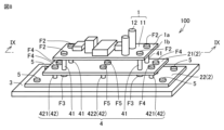
- FIG. 1 is a perspective view schematically showing the configuration of an electronic device according to Embodiment 1;
- FIG. FIG. 2 is a cross-sectional view taken along line II-II of FIG. 1;
- 2 is a plan view schematically showing the configuration of the circuit board of the electronic device according to Embodiment 1;
- FIG. 2 is a plan view schematically showing the configuration of an insulating plate of the electronic device according to Embodiment 1;
- FIG. 2 is a plan view schematically showing the configuration of the circuit board of the electronic device according to Embodiment 1;
- FIG. FIG. 4 is a cross-sectional view schematically showing the configuration of an electronic device according to a modification of Embodiment 1;
- FIG. 3 is a cross-sectional view schematically showing the configuration of an electronic device according to a comparative example
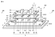
- FIG. 10 is a perspective view schematically showing the configuration of an electronic device according to Embodiment 2
- FIG. 9 is a cross-sectional view taken along line IX-IX of FIG. 8
- FIG. 11 is a plan view schematically showing the configuration of a first insulating portion of an electronic device according to Embodiment 2
- FIG. 8 is a plan view schematically showing the configuration of a second insulating portion of an electronic device according to Embodiment 2
- FIG. 11 is a perspective view schematically showing the configuration of an electronic device according to Embodiment 3
- FIG. 13 is a cross-sectional view along line XIII-XIII of FIG. 12;
- FIG. 11 is a plan view schematically showing the configuration of a third insulating portion of an electronic device according to Embodiment 3;
- FIG. 11 is a plan view schematically showing the configuration of a fourth insulating portion of an electronic device according to Embodiment 3;
- FIG. 11 is a plan view schematically showing the configuration of a fifth insulating portion of an electronic device according to Embodiment 3;
- FIG. 11 is a cross-sectional view schematically showing the configuration of an electronic device according to a first modification of the third embodiment;
- FIG. 12 is a perspective view schematically showing the configuration of an electronic device according to a second modification of the third embodiment;
- FIG. 19 is a cross-sectional view along line XIX-XIX in FIG. 18;
- FIG. 19 is a cross-sectional view along line XIX-XIX in FIG. 18;
- FIG. 21 is a top view schematically showing the configuration of a third insulating portion of an electronic device according to a second modification of the third embodiment
- FIG. 20 is a bottom view schematically showing a configuration of a fourth insulating portion of an electronic device according to a second modified example of the third embodiment
- FIG. 20 is a perspective view schematically showing the configuration of an electronic device according to a third modified example of the third embodiment
- FIG. 23 is a cross-sectional view taken along line XXIII-XXIII of FIG. 22
- FIG. 21 is a side view schematically showing the configuration of an insulating plate and an insulating support member of an electronic device according to a third modification of the third embodiment
- FIG. 20 is a top view schematically showing the configuration of an insulating plate and an insulating supporting member of an electronic device according to a third modification of the third embodiment
- FIG. 12 is a perspective view schematically showing the configuration of an electronic device according to Embodiment 4
- FIG. 27 is a cross-sectional view along line XXVII-XXVII of FIG. 26
- FIG. 11 is a plan view schematically showing the configuration of an insulating plate of an electronic device according to Embodiment 4
- FIG. 12 is a perspective view schematically showing the configuration of an electronic device according to Embodiment 5
- FIG. 30 is a cross-sectional view along line XXX-XXX in FIG. 29;
- FIG. 11 is a plan view schematically showing the configuration of an insulating plate of an electronic device according to Embodiment 5;
- FIG. 11 is a side view schematically showing the configuration of an insulating plate of an electronic device according to Embodiment 5;
- FIG. 11 is a plan view schematically showing the configuration of a housing of an electronic device according to Embodiment 5;
- FIG. 13 is a perspective view schematically showing the configuration of a fixture for electronic equipment according to Embodiment 5;
- Embodiment 1 The configuration of electronic device 100 according to the first embodiment will be described with reference to FIGS. 1 to 5.
- FIG. 1 A diagrammatic representation of electronic device 100 according to the first embodiment will be described with reference to FIGS. 1 to 5.
- electronic device 100 is, for example, a control device.
- Electronic device 100 mainly includes circuit board 1 , insulating plate 2 , housing 3 , insulating support member 4 , and fixing portion 5 .
- the configuration of electronic device 100 will be described using the thickness direction and the in-plane direction.
- the thickness direction crosses the in-plane direction.
- the thickness direction is orthogonal to the in-plane direction.
- the circuit board 1 includes a board portion 11 and a conductive member 12.
- the substrate portion 11 includes a first surface 1a and a second surface 1b.
- a conductive member 12 is mounted on the substrate portion 11 .
- the conductive member 12 has conductivity.
- the conductive member 12 is, for example, an electronic component, an electrical component, a metal wiring pattern, or the like.
- the substrate portion 11 has a flat plate shape.
- a conductive member 12 is arranged on the first surface 1a.
- the second surface 1b faces the first surface 1a.
- the conductive member 12 is not arranged on the second surface 1b.
- the second surface 1b faces the first surface 1a along the thickness direction.
- the circuit board 1 extends along the in-plane direction.
- the board portion 11 is made of a printed board member such as paper phenol, glass epoxy resin, or the like.
- the thickness of the substrate portion 11 is, for example, 0.4 mm or more and 3.2 mm or less.
- the width and length of the substrate portion 11 are, for example, 25 mm or more and 550 mm or less.
- the insulating plate 2 is arranged on the side opposite to the first surface 1a with respect to the second surface 1b.
- the insulating plate 2 has insulating properties.
- the insulating plate 2 is made of, for example, insulating resin such as epoxy resin.
- the insulating plate 2 extends along the in-plane direction.
- the insulating plate 2 has an in-plane dimension larger than that of the circuit board 1 .
- the housing 3 is in contact with the insulating plate 2 on the side opposite to the circuit board 1 with respect to the insulating plate 2 .
- the housing 3 is arranged without leaving an interval from the insulating plate 2 . It is desirable that the housing 3 is in contact with the insulating plate 2 without gaps.
- An insulating plate 2 is fixed to the housing 3 .
- the housing 3 has an in-plane dimension larger than that of the insulating plate 2 .
- the housing 3 has conductivity.
- the housing 3 is made of metal.
- the housing 3 is made of, for example, iron and steel typified by steel and iron-containing alloys.
- the housing 3 is made of, for example, a non-ferrous metal such as an alloy containing a metal such as aluminum (Al) or copper (Cu).
- the insulating support member 4 supports the circuit board 1 on the insulating plate 2 .
- An insulating support member 4 is interposed between the circuit board 1 and the insulating plate 2 .
- the insulating support member 4 has portions exposed from the circuit board 1 and the insulating plate 2 over the entire circumference.
- One end of insulating support member 4 is fixed to circuit board 1 by each of a plurality of first fixtures F1.
- insulating support 4 includes a plurality of spacers 40 .
- the insulating support 4 contains, for example, four spacers 40 .
- Each of the plurality of spacers 40 supports the circuit board 1 on the insulating plate 2 .
- Each of the plurality of spacers 40 has the same shape as each other.
- Each of the plurality of spacers 40 is the same as the insulating support material 4 .
- the insulating support material 4 is electrically insulated from the housing 3.
- the circuit board 1 supported by the insulating support member 4 is also electrically insulated from the housing 3 .
- the other end of the insulating support member 4 is embedded in the insulating plate 2 .
- the other end of the insulating support member 4 does not penetrate the insulating plate 2 .
- the other end of the insulating support member 4 is not in contact with the housing 3 .
- the other end of the insulating support member 4 is electrically insulated from the housing 3 .
- the insulating support member 4 is configured separately from the insulating plate 2 and the housing 3 .
- the insulating support material 4 has insulating properties.
- the insulating support member 4 is made of an insulating material such as Duracon (registered trademark) or nylon.
- the shape of the insulating support member 4 is, for example, linear.
- the insulating support member 4 may be configured as an insulator as described below.
- the second surface 1 b of the circuit board 1 is spaced apart from the insulating plate 2 by the insulating support material 4 .
- the insulating plate 2 is not in contact with the second surface 1 b of the circuit board 1 .
- the entire second surface 1 b of the circuit board 1 is spaced apart from the insulating plate 2 by the insulating support member 4 .
- the circuit board 1 and the insulating plate 2 are connected only through the insulating support member 4 .
- the fixing part 5 fixes the insulating plate 2 to the housing 3 .
- the fixing portion 5 fixes the insulating plate 2 to the housing 3 by mechanically fastening the insulating plate 2 to the housing 3 .
- the fixing portion 5 is configured by, for example, a plurality of rivets 50 (see FIG. 1).
- the fixing portion 5 is a rivet
- the rivet is processed by a riveter tool in a state in which the rivet penetrates the first through portion H1 of the insulating plate 2 and the pilot hole of the housing 3, thereby fixing the insulating plate 2 to the housing. It is fixed to the body 3.
- the fixing portion 5 may be configured by, for example, a plurality of screws.
- the fixing part 5 is a screw
- the housing 3 is provided with a nut in advance by crimping, and the insulating plate 2 is fixed to the housing 3 by screwing the screw to the nut.
- the fixed part 5 has conductivity.
- the fixed portion 5 is made of metal such as aluminum (Al) or stainless steel.
- the fixing part 5 is the same as each of the rivets or each of the screws.
- the fixing part 5 is arranged outside the circuit board 1 when the circuit board 1 and the fixing part 5 are viewed along the direction from the first surface 1a to the second surface 1b.
- the fixing portion 5 is exposed from the circuit board 1 when the fixing portion 5 is viewed along the direction from the first surface 1a to the second surface 1b.
- the creepage distance and the spatial distance from the fixed portion 5 to the conductive member 12 are longer than the creepage distance and the spatial distance from the conductive member 12 to the insulating plate 2 .
- the plurality of first fixtures F1 fix the circuit board 1 to the insulating support member 4.
- the plurality of first fixtures F1 fix the circuit board 1 to the insulating support member 4 by mechanically fastening the circuit board 1 to the insulating support member 4 .
- a plurality of first fixtures F1 are fixed to the insulating support member 4 while passing through the substrate portion 11 .
- Each of the multiple first fixtures F1 is configured by, for example, a screw.
- the screw is, for example, a pan screw, and is made of metal such as iron (Fe), stainless steel, or brass.
- the multiple first fixtures F1 are conductive.
- the circuit board 1 is provided with a plurality of insertion holes IH.
- a first fixture F1 (see FIG. 2) is inserted into each of the plurality of insertion holes IH.
- the plurality of insertion holes IH are configured as female threads.
- Each of the four corners of the circuit board 1 is provided with a plurality of insertion holes IH.
- the insulating plate 2 is provided with a plurality of first penetrating portions H1 and a plurality of first engaging portions E1.
- a fixing portion 5 (see FIG. 2) is inserted into each of the plurality of first penetrating portions H1.
- Each of the four corners of the insulating plate 2 is provided with a plurality of first penetrating portions H1.
- the plurality of first engaging portions E1 do not penetrate the insulating plate 2 .
- the plurality of first engaging portions E1 are configured as screw holes, for example.
- An insulating support member 4 (see FIG. 2) is fixed to each of the plurality of first engaging portions E1.
- the plurality of first penetrating portions H1 are arranged outside the plurality of first engaging portions E1.
- the shortest distance along the surface of the insulating plate 2 from each first penetrating portion H1 to the first engaging portion E1 arranged in the immediate vicinity of the first penetrating portion H1 is The same is true for each of the plurality of first engaging portions E1.
- the housing 3 is provided with a plurality of through holes TH.
- a fixing portion 5 (see FIG. 2) is inserted into each of the plurality of through holes TH.
- Each of the four corners of the housing 3 is provided with a plurality of through holes.
- the insulation distance for insulation between the circuit board 1 and the housing 3 includes a creepage distance and a spatial distance.
- the creepage distance is the shortest distance between the circuit board 1 and the housing 3 via an insulator. In FIG. 2, the creepage distance is indicated by a solid arrow.
- the spatial distance is the shortest distance between the circuit board 1 and the housing 3 through the air. In FIG. 2, the spatial distances are indicated by dashed arrows.
- the creepage distance is the shortest distance f1 along the first surface 1a of the circuit board 1 between the conductive member 12 (metal wiring pattern) of the circuit board 1 and the first fixture F1, It is the sum (f1+a1+g1) of the shortest distance a1 along the surface of the insulating support member 4 to the plate 2 and the shortest distance g1 along the surface of the insulating plate 2 between the insulating support member 4 and the fixed portion 5.
- the shortest distance a1 is also the dimension in the thickness direction of the insulating support member 4 between the circuit board 1 and the insulating plate 2. As shown in FIG.
- the creepage distance in the present embodiment is the shortest creepage distance from conductive member 12 of circuit board 1 to fixed portion 5 via insulating support member 4 and insulating plate 2 .
- the shortest creepage distance of this embodiment is designed to satisfy the creepage distance required by the standard.
- the insulation performance (withstand voltage value) of the electronic device 100 increases as the creepage distance (f1+a1+g1) increases. Therefore, the larger the in-plane dimension of the insulating plate 2, the longer the shortest distance g1 along the surface of the insulating plate 2 between the insulating support member 4 and the fixed portion 5, and the longer the creeping distance (f1+a1+g1). Therefore, the larger the dimension of the insulating plate 2 in the in-plane direction, the higher the insulating performance (withstand voltage value) of the electronic device 100 .
- the spatial distance h1 is the sum of the shortest distance between the fixing portion 5 and the first fixture F1 and the shortest distance between the first fixture F1 and the conductive member 12 of the circuit board 1.
- the creepage distance (f1+a1+g1) is longer than the clearance h1.
- the creepage distance required for insulation between the circuit board 1 and the housing 3 is longer than the spatial distance required for insulation between the circuit board 1 and the housing 3 .
- the spatial distance required for insulation between the circuit board 1 and the housing 3 is h1
- the creepage distance required for insulation between the circuit board 1 and the housing 3 is (1.5 ⁇ h1).
- the circuit board 1 and the housing 3 are insulated if the creepage distance (f1+a1+g1) is (1.5 ⁇ h1) or more.
- the creepage distance and the clearance are increased without increasing the dimension in the thickness direction of the electronic device 100 . That is, the expansion of the dimension of the electronic device 100 in the thickness direction is suppressed while ensuring both the creepage distance and the clearance between the circuit board 1 and the housing 3 and the insulation performance.
- the insulating support material 4 may be configured as an insulator.
- the insulating support member 4 configured as an insulator includes a shaft portion 4a and a plurality of projecting portions 4b projecting from the shaft portion 4a.
- the shortest distance a1 between the circuit board 1 and the insulating plate 2 along the surface of the insulating support member 4 is increased while the thickness dimension of the insulating support member 4 is maintained.
- the insulation performance (withstand voltage value) of the electronic device 100 is increased.
- the standard requires that the creepage distance be longer than the spatial distance, but if the creepage distance is excessively longer than the spatial distance, the electronic device 100 becomes excessively large. That is, if there is an extra length difference between the creepage distance and the spatial distance, the electronic device 100 becomes excessively large. The extra length difference between the creepage distance and the clearance distance is reduced by the insulator.
- the electronic device 101 does not include the insulating plate 2 (see FIG. 2).
- the circuit board 1 is supported by the housing 3 by linear spacers 40 .
- the insulation distance between the circuit board 1 and the housing 3 is maintained by the length L of the spacer 40 .
- JEM Joint Electrical Manufacturers' Association
- the spatial distance is 60 mm or more.
- a creepage distance of 90 mm or more must be secured.
- the length of the spacer 40 is 90 mm in order to satisfy the insulation distance between the circuit board 1 and the housing 3.
- the spatial distance is 60 mm or more
- the linear spacer 40 is used, it is necessary to ensure a creepage distance of 90 mm or more.
- the resonance frequency of the circuit board 1 may be low. Therefore, the resonance frequency of the circuit board 1 may be included in the vibration frequency band of the structure of the electronic device 101 .
- the circuit board 1 When the circuit board 1 resonates with the structure of the electronic device 101, the amplitude of heavy objects such as electronic components mounted on the circuit board 1 may be amplified. As a result, the circuit board 1 vibrates violently, and the circuit board 1 may be destroyed by the vibration. Vibration of the circuit board 1 can occur in the thickness direction and the in-plane direction. Breakage due to vibration of the circuit board 1 on which a heavy object is mounted includes, for example, breakage of connection points between terminals of heavy electronic components such as transformers, capacitors, and reactors and the circuit board 1, breakage of terminals, and the like. That is, the electronic device 101 according to the comparative example has a problem of low vibration resistance.
- a configuration in which the circuit board 1 and the housing 3 are fixed via an insulator may be adopted.
- the creepage distance between the circuit board 1 and the housing 3 is ensured by the uneven structure of the insulator. Therefore, the creepage distance is ensured with an insulator having a length shorter than that of the straight spacer 40 .
- the in-plane dimension of the circuit board 1 needs to be further increased. That is, when the insulation distance is ensured only by the insulator, there is a problem that the dimension of the electronic device in the in-plane direction becomes large due to the above.
- second surface 1b of circuit board 1 is spaced apart from insulating plate 2 by insulating support member 4. there is Therefore, the insulating distance between the circuit board 1 and the housing 3 is ensured by the combination of the insulating plate 2 and the insulating support member 4 . Therefore, it is possible to suppress the dimension of the electronic device 100 from increasing in the thickness direction as compared with the case where the insulation distance is secured only by the linear spacer 40 (see FIG. 7), and the case where the insulation distance is secured only by the insulator. It is possible to prevent the in-plane dimension of the electronic device 100 from increasing.
- the natural frequency of the circuit board 1 can be increased, and the natural frequency of the circuit board 1 can be made different from the vibration frequency in the structure of the electronic device 100, so that the vibration resistance of the circuit board 1 can be improved. be able to.
- outside air can flow in the space between the second surface 1b of the circuit board 1 and the insulating plate 2, heat dissipation from the conductive member 12 mounted on the circuit board 1 can be realized.
- air exists between the second surface 1b of the circuit board 1 and the insulating plate 2 the risk of discharge and creeping discharge caused by voids is reduced.
- the second surface 1 b of the circuit board 1 is spaced apart from the insulating plate 2 by the insulating support member 4 . Therefore, the second surface 1b of the circuit board 1 and the insulating plate 2 do not come into contact with each other. If it is necessary to bring the entire second surface 1b of the circuit board 1 into contact with the insulating plate 2, defects such as voids and gaps may occur between the second surface 1b and the insulating plate 2, causing defects. Such partial discharge may occur, the insulating plate 2 may deteriorate, and dielectric breakdown may occur. Further, if the insulating plate 2 in contact with the second surface 1b of the circuit board 1 contains impurities, the creeping discharge initiating voltage is reduced.
- a creeping discharge caused by the defect may occur, and dielectric breakdown may occur.
- the electronic device 100 according to the present embodiment it is not necessary to bring the second surface 1b of the circuit board 1 and the insulating plate 2 into contact with each other. It is possible to suppress the occurrence of defects such as voids and voids. Therefore, it is possible to suppress the occurrence of dielectric breakdown caused by defects in the insulating plate 2 .
- the fixing portion 5 is arranged outside the circuit board 1 when the circuit board 1 and the fixing portion 5 are viewed along the direction from the first surface 1a to the second surface 1b. ing. Therefore, the spatial distance h1 between the circuit board 1 and the housing 3 can be made larger than when the fixing portion 5 is arranged inside the circuit board 1 . Further, for example, the spatial distance h1 between the circuit board 1 and the housing 3 can be made larger than when the circuit board 1 and the housing 3 are connected by a linear spacer 40 (see FIG. 7). . Therefore, the insulation performance (withstand voltage value) of the housing 3 can be improved.
- Embodiment 2 Next, the configuration of electronic device 100 according to the second embodiment will be described with reference to FIGS. 8 to 11.
- FIG. The second embodiment has the same configuration and effects as those of the first embodiment unless otherwise specified. Therefore, the same reference numerals are given to the same configurations as in the above-described first embodiment, and description thereof will not be repeated.
- the insulating plate 2 of the electronic device 100 includes a first insulating portion 21 and a second insulating portion 22 .
- the first insulating portion 21 is connected to the circuit board 1 .
- the second insulating portion 22 is in contact with the housing 3 .
- the first insulating portion 21 and the second insulating portion 22 are viewed along the direction from the first surface 1a to the second surface 1b, the first insulating portion 21 and the second insulating portion 2
- the insulating part 22 is larger than the circuit board 1 .
- the first insulating portion 21 and the second insulating portion 22 have an area larger than that of the circuit board 1 .
- the second insulating portion 22 is larger than the first insulating portion 21 when the first insulating portion 21 and the second insulating portion 22 are viewed along the direction from the first surface 1a toward the second surface 1b.
- the second insulating portion 22 has an area larger than that of the first insulating portion 21 .
- the insulating support member 4 includes a first support portion 41 and a second support portion 42 .
- the first supporting portion 41 supports the circuit board 1 on the first insulating portion 21 .
- the first support portion 41 and the second support portion 42 include a plurality of spacers.
- One end of the first support portion 41 is fixed to the circuit board 1 by each of the plurality of second fixtures F2.
- the other end of the first support portion 41 is fixed to the first insulating portion 21 by each of the plurality of third fixtures F3.
- the first support portion 41 and the second support portion 42 are the same as each of the plurality of spacers.
- the second supporting portion 42 supports the first insulating portion 21 on the second insulating portion 22 .
- the second support portion 42 is arranged to be displaced from the first support portion 41 in the in-plane direction.
- the second support portion 42 is not arranged on the same imaginary straight line extending in the thickness direction with respect to the first support portion 41 .
- the second support portion 42 has a first portion 421 and a second portion 422 .
- Each of the first portion 421 and the second portion 422 supports the first insulating portion 21 to the second insulating portion 22 .
- One end of the first portion 421 is fixed to the first insulating portion 21 by each of the plurality of fourth fixtures F4.
- One end of the second portion 422 is fixed to the first insulating portion 21 by each of the plurality of fifth fixtures F5.
- the other end of the first portion 421 and the other end of the second portion 422 are fixed to the second insulating portion 22 by being screwed into the second insulating portion 22 .
- the first portion 421 extends outside the circuit board 1 .
- the second portion 422 is arranged inside the circuit board 1 , and the first support portion 41 is arranged so as to be sandwiched between the first portion 421 and the second portion 422 .
- the first portion 421 is exposed from the circuit board 1 when the circuit board 1 and the first support portion 41 are viewed along the direction from the first surface 1a to the second surface 1b.
- the circuit board 1 overlaps the second portion 422 .
- the first support portion 41 is arranged between the first portion 421 and the second portion 422 .
- the first support portion 41 and the first portion 421 are not arranged on the same imaginary straight line extending in the thickness direction.
- the first support portion 41 and the second portion 422 are not arranged on the same imaginary straight line extending in the thickness direction.
- the second surface 1b of the circuit board 1 is spaced apart from the first insulating portion 21 by the first supporting portion 41.
- the entire second surface 1 b of the circuit board 1 is spaced apart from the first insulating portion 21 by the first supporting portion 41 .
- the first insulating portion 21 is not in contact with the circuit board 1 .
- the first insulating portion 21 is spaced apart from the circuit board 1 in the direction from the first surface 1a to the second surface 1b.
- the first supporting portion 41 is exposed from the circuit board 1 and the first insulating portion 21 over the entire circumference.
- the first insulating portion 21 is spaced apart from the second insulating portion 22 by the second support portion 42 .
- the first insulating portion 21 is not in contact with the second insulating portion 22 .
- the first insulating portion 21 is spaced apart from the second insulating portion 22 in the direction from the first surface 1a toward the second surface 1b.
- the second support portion 42 has portions exposed from the first insulating portion 21 and the second insulating portion 22 over the entire circumference.
- the fixing part 5 fixes the second insulating part 22 to the housing 3 .
- a plurality of second fixtures F2 fix the circuit board 1 to the first support portion 41 .
- a plurality of third fixtures F3 fix the first insulating portion 21 to the first support portion 41 .
- a plurality of fourth fixtures F4 fix the first insulating portion 21 to the first portion 421 .
- a plurality of fifth fixtures F5 fix the first insulating portion 21 to the second portion 422 .
- Each of the plurality of second fixtures F2, the plurality of third fixtures F3, the plurality of fourth fixtures F4, and the plurality of fifth fixtures F5 is configured by, for example, a screw.
- the plurality of second fixtures F2, the plurality of third fixtures F3, the plurality of fourth fixtures F4, and the plurality of fifth fixtures F5 are conductive.
- the first insulating portion 21 is provided with a plurality of second through portions H2, a plurality of third through portions H3 and a plurality of fourth through portions H4.
- a first support portion 41 (see FIG. 9) is fixed to each of the plurality of second through portions H2 by each of a plurality of third fixtures F3 (see FIG. 9).
- the first portion 421 (see FIG. 9) is fixed to each of the plurality of third through portions H3 by each of the plurality of fourth fixtures F4 (see FIG. 9).
- the second portion 422 (see FIG. 9) is fixed to each of the plurality of fourth through portions H4 by each of the plurality of fifth fixtures F5 (see FIG. 9).
- Each of the plurality of third penetrating portions H3 is provided at the four corners of the first insulating portion 21 away from each of the plurality of second penetrating portions H2. Desirably, the shortest distance along the surface of the first insulating portion 21 from each third penetrating portion H3 to the second penetrating portion H2 disposed in the immediate vicinity of the third penetrating portion H3 is and each of the plurality of third penetrating portions H3.
- a plurality of fourth penetrating portions H4 are provided in the center of the first insulating portion 21 . The shortest distance along the surface of the first insulating portion 21 from the third through portion H3 to the second through portion H2 is shorter than the shortest distance from the fourth through portion H4 to the second through portion H2.
- the second insulating portion 22 is provided with a plurality of second engaging portions E2, a plurality of third engaging portions E3, and a plurality of fifth penetrating portions H5.
- the plurality of second engaging portions E2 and the plurality of third engaging portions E3 do not penetrate the second insulating portion 22 .
- the plurality of second engaging portions E2 and the plurality of third engaging portions E3 are configured as screw holes, for example.
- a first portion 421 (see FIG. 9) is fixed to each of the plurality of second engaging portions E2.
- a second portion 422 (see FIG. 9) is fixed to each of the plurality of third engaging portions E3.
- the fixing portion 5 penetrates through each of the plurality of fifth penetrating portions H5.
- Each of the multiple fifth penetrating portions H5 is provided at each of the four corners of the second insulating portion 22 .
- the plurality of second engaging portions E2 and the plurality of third engaging portions E3 are arranged inside the plurality of fifth through portions H5.
- the creepage distance is the shortest distance f2 along the first surface 1a of the circuit board 1 between the conductive member 12 of the circuit board 1 and the second fixture F2,
- the shortest distance a2 along the surface of the first support portion 41, the shortest distance b2 along the surface of the first insulating portion 21 between the third fixture F3 and the fourth fixture F4, the first insulating portion 21 and the second The sum of the shortest distance c2 along the surface of the second support portion 42 with the insulating portion 22 and the shortest distance g2 along the surface of the second insulating portion 22 between the second engaging portion E2 and the fixing portion 5 (f2+a2+b2+c2+g2) be.
- the creeping distance (f2+a2+b2+c2+g2) of the present embodiment is from the conductive member 12 of the circuit board 1 to the housing 3 via the first supporting portion 41, the first insulating portion 21, the second supporting portion 42 and the second insulating portion 22. is the shortest creepage distance of The creepage distance (f2+a2+b2+c2+g2) is designed to satisfy the creepage distance required by the standard.
- the spatial distance h2 is the sum of the shortest distance between the fixing portion 5 and the second fixture F2 and the shortest distance between the second fixture F2 and the conductive member 12 of the circuit board 1.
- the creepage distance (f2+a2+b2+c2+g2) is longer than the clearance h2.
- the insulation performance (withstand voltage value) of the electronic device 100 increases as the creepage distance (f2+a2+b2+c2+g2) increases.
- the in-plane dimension of the insulating plate 2 increases, the shortest distance g2 along the surface of the second insulating portion 22 between the second engaging portion E2 and the fixture increases, so the creepage distance (f2+a2+b2+c2+g2) increases. . Therefore, as the in-plane dimension of the insulating plate 2 increases, the insulating performance (withstand voltage value) of the electronic device 100 improves. Also, the unnecessary length difference between the creepage distance and the clearance is reduced.
- the creepage distance required for insulation between the circuit board 1 and the housing 3 is longer than the spatial distance required for insulation between the circuit board 1 and the housing 3 .
- the spatial distance required for insulation between the circuit board 1 and the housing 3 is h2
- the creepage distance required for insulation between the circuit board 1 and the housing 3 is (1.5 ⁇ h2).
- the creepage distance (f2+a2+b2+c2+g2) is (1.5 ⁇ h2) or more
- the circuit board 1 and the housing 3 are insulated.
- the creepage distance and the clearance are increased without increasing the dimension in the thickness direction of the electronic device 100 . That is, the expansion of the dimension of the electronic device 100 in the thickness direction is suppressed while ensuring both the creepage distance and the clearance between the circuit board 1 and the housing 3 and the insulation performance.
- the first support portion 41 and the second support portion 42 may have an insulator structure.
- the shortest distance a2 between the circuit board 1 and the insulating plate 2 along the surface of the first supporting portion 41 and the distance between the first insulating portion 21 and the second insulating portion 22 along the surface of the second supporting portion 42 The shortest distance c2 becomes longer. Therefore, the creepage distance (f2+a2+b2+c2+g2) can be increased without increasing the dimension of the electronic device 100 in the thickness direction. Also, the extra length difference between the creepage distance and the clearance distance is further reduced.
- the second surface 1b of the circuit board 1 is spaced apart from the first insulating portion 21 by the first supporting portion 41.
- the first insulating portion 21 is spaced apart from the second insulating portion 22 by the second support portion 42 . Therefore, the creepage distance and the spatial distance between the circuit board 1 and the housing 3 can be increased. Therefore, the withstand voltage value of the electronic device 100 can be increased. Since the creepage distance can be increased, it is possible to suppress an increase in the dimension of the electronic device 100 in the in-plane direction.
- the dimension in the thickness direction of the electronic device 100 can be changed. It is also possible to increase the creepage distance and the spatial distance between the circuit board 1 and the housing 3.
- the first portion 421 is the circuit. It is arranged outside the substrate 1 , the second portion 422 is arranged inside the circuit board 1 , and the first support portion 41 is arranged so as to be sandwiched between the first portion 421 and the second portion 422 . Therefore, the natural frequency of the circuit board 1 can be increased more than when the first supporting portion 41, the first portion 421 and the second portion 422 are arranged on the same imaginary straight line extending in the thickness direction. can. Therefore, the natural frequency of the circuit board 1 can be made different from the vibration frequency band in the structure of the electronic device 100 . Therefore, the vibration resistance of the circuit board 1 can be improved.
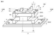
- FIG. Embodiment 3 has the same configuration and effects as those of Embodiment 1 described above unless otherwise specified. Therefore, the same reference numerals are given to the same configurations as in the above-described first embodiment, and description thereof will not be repeated.
- the insulating plate 2 of the electronic device 100 includes a third insulating portion 23, a fourth insulating portion 24, and a fifth insulating portion 25.
- the third insulating portion 23 is connected to the circuit board 1 .
- the fourth insulating portion 24 is connected to the third insulating portion 23 on the side opposite to the housing 3 with respect to the third insulating portion 23 .
- the fourth insulating portion 24 may have the same shape as the third insulating portion 23 .
- the third insulating portion 23 and the fourth insulating portion 24 are made of, for example, insulating resin such as epoxy resin, insulating paper, or film.
- the fifth insulating portion 25 is in contact with the housing 3 .
- the fifth insulating portion 25 has an area larger than that of the third insulating portion 23 and the fourth insulating portion 24 .
- the fifth insulating portion 25 is thicker than the third insulating portion 23 and the fourth insulating portion 24 .
- the fifth insulating portion 25 is made of resin such as epoxy resin, for example.
- the insulating support member 4 includes a third support portion 43, a fourth support portion 44, and a fifth support portion 45.
- the third support portion 43, the fourth support portion 44 and the fifth support portion 45 include a plurality of spacers.
- the third supporting portion 43, the fourth supporting portion 44 and the fifth supporting portion 45 are the same as each of the plurality of spacers.
- the third supporting portion 43 supports the circuit board 1 on the third insulating portion 23 .
- One end of the third support portion 43 is fixed to the circuit board 1 by each of the plurality of sixth fixtures F6.
- the other end of the third support portion 43 is fixed to the first insulating portion 21 by each of the plurality of seventh fixtures F7.
- the fourth support portion 44 supports the third insulating portion 23 on the fourth insulating portion 24 .
- One end of the fourth support portion 44 is fixed to the third insulating portion 23 by each of the plurality of eighth fixtures F8.
- the other end of the fourth support portion 44 is fixed to the fourth insulating portion 24 by each of the plurality of ninth fixtures F9.
- the fifth support portion 45 supports the fourth insulating portion 24 on the fifth insulating portion 25 .
- the fifth support portion 45 is fixed to the fourth insulating portion 24 by each of the plurality of tenth fixtures F10.
- the plurality of sixth fixtures F6, the plurality of seventh fixtures F7, the plurality of eighth fixtures F8, the plurality of ninth fixtures F9, and the plurality of tenth fixtures F10 are conductive.
- Each of the plurality of sixth fixtures F6, the plurality of seventh fixtures F7, the plurality of eighth fixtures F8, the plurality of ninth fixtures F9, and the plurality of tenth fixtures F10 is configured by, for example, a screw.
- the second surface 1 b of the circuit board 1 is spaced apart from the third insulating portion 23 by the third supporting portion 43 .
- the entire second surface 1 b of the circuit board 1 is spaced apart from the third insulating portion 23 by the third supporting portion 43 .
- the third insulating portion 23 is not in contact with the circuit board 1 .
- the third insulating portion 23 is spaced apart from the circuit board 1 in the direction from the first surface 1a to the second surface 1b.
- the third supporting portion 43 is exposed from the circuit board 1 and the third insulating portion 23 over the entire circumference.
- the third insulating portion 23 is spaced apart from the fourth insulating portion 24 by the fourth support portion 44 .
- the third insulating portion 23 is not in contact with the fourth insulating portion 24 .
- the third insulating portion 23 is spaced apart from the fourth insulating portion 24 in the direction from the first surface 1a toward the second surface 1b.
- the fourth support portion 44 is exposed from the third insulating portion 23 and the fourth insulating portion 24 over the entire circumference.
- the fourth insulating portion 24 is spaced apart from the fifth insulating portion 25 by the fifth support portion 45 .
- the fourth insulating portion 24 is not in contact with the fifth insulating portion 25 .
- the fourth insulating portion 24 is spaced apart from the fifth insulating portion 25 in the direction from the first surface 1a toward the second surface 1b.
- the fifth support portion 45 has portions exposed from the fourth insulating portion 24 and the fifth insulating portion 25 over the entire circumference.
- the fourth insulating portion 24 includes the third insulating portion 23 and the fifth insulating portion It is arranged inside the portion 25 .
- the fourth insulating portion 24 is not arranged on the same imaginary straight line extending in the thickness direction with respect to the third insulating portion 23 or the fifth insulating portion 25 .
- the third insulating portion 23 and the fifth insulating portion 25 may be arranged on the same imaginary straight line extending in the thickness direction.
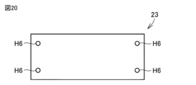
- the third insulating portion 23 is provided with a plurality of sixth penetrating portions H6 and a plurality of seventh penetrating portions H7.
- a third support portion 43 (see FIG. 13) is fixed to each of the plurality of sixth through portions H6 by a plurality of seventh fixtures F7 (see FIG. 13).
- a fourth support portion 44 (see FIG. 13) is fixed to each of the plurality of seventh penetrating portions H7 by each of a plurality of eighth fixtures F8 (see FIG. 13).
- the plurality of seventh penetrating portions H7 are arranged inside the plurality of sixth penetrating portions H6.
- Each of the plurality of seventh penetrating portions H7 is provided at the four corners of the third insulating portion 23 away from each of the plurality of sixth penetrating portions H6. Desirably, the shortest distance along the surface of the third insulating portion 23 from each seventh penetrating portion H7 to the sixth penetrating portion H6 arranged in the immediate vicinity of the seventh penetrating portion H7 is and each of the plurality of seventh penetrating portions H7.
- the fourth insulating portion 24 is provided with a plurality of eighth penetrating portions H8 and a plurality of ninth penetrating portions H9.
- a fourth support portion 44 (see FIG. 13) is fixed to each of the plurality of eighth penetrating portions H8 by a plurality of ninth fixtures F9 (see FIG. 13).
- a fifth support portion 45 (see FIG. 13) is fixed to each of the plurality of ninth penetrating portions H9 by each of a plurality of tenth fixtures F10 (see FIG. 13).
- the plurality of eighth penetrating portions H8 are arranged inside the plurality of ninth penetrating portions H9.
- Each of the plurality of ninth penetrating portions H9 is provided at the four corners of the fourth insulating portion 24 apart from each of the plurality of eighth penetrating portions H8. Desirably, the shortest distance along the surface of the fourth insulating portion 24 from each ninth penetrating portion H9 to the eighth penetrating portion H8 arranged in the immediate vicinity of the ninth penetrating portion H9 is and each of the plurality of ninth penetrating portions H9.
- the fifth insulating portion 25 is provided with a plurality of fourth engaging portions E4 and a plurality of tenth penetrating portions H10.
- the multiple fourth engaging portions E4 do not penetrate the fifth insulating portion 25 .
- the plurality of fourth engaging portions E4 are configured as screw holes, for example.
- a fifth support portion 45 (see FIG. 13) is fixed to each of the plurality of fourth engagement portions E4.
- the plurality of tenth penetrating portions H10 are provided at the four corners of the fifth insulating portion 25, respectively.
- the plurality of fourth engaging portions E4 are arranged inside the plurality of tenth penetrating portions H10.
- Each of the plurality of tenth penetrating portions H10 is provided at the four corners of the fifth insulating portion 25 away from each of the plurality of fourth engaging portions E4. Desirably, the shortest distance along the surface of the fifth insulating portion 25 from each tenth penetrating portion H10 to the fourth engaging portion E4 arranged in the immediate vicinity of the tenth penetrating portion H10 is a plurality of fourth engaging portions H10. The same is true for the portion E4 and each of the tenth penetrating portions H10.
- the creepage distance is the shortest distance f3 along the first surface 1a of the circuit board 1 between the conductive member 12 of the circuit board 1 and the sixth fixture F6,
- the creepage distance (f3+a3+b3+c3+d3+e3+f3+g3) of the present embodiment is from the conductive member 12 of the circuit board 1 to the third supporting portion 43, the third insulating portion 23, the fourth supporting portion 44, the fourth insulating portion 24, the fifth supporting portion 45 and It is the shortest creepage distance to the housing 3 via the fifth insulating portion 25 .
- the creepage distance (f3+a3+b3+c3+d3+e3+f3+g3) is designed to satisfy the creepage distance required by the standard.
- the spatial distance h3 is the sum of the shortest distance between the fixing portion 5 and the sixth fixture F6 and the shortest distance between the sixth fixture F6 and the conductive member 12 of the circuit board 1.
- the creepage distance (f3+a3+b3+c3+d3+e3+f3+g3) is longer than the clearance h3.
- the insulation performance (withstand voltage value) of the electronic device 100 increases as the creepage distance (f3+a3+b3+c3+d3+e3+f3+g3) increases.
- the in-plane dimension of the insulating plate 2 increases, the shortest distance g3 along the surface of the fifth insulating portion 25 between the fourth engaging portion E4 and the fixing portion 5 increases, so the creepage distance (f3+a3+b3+c3+d3+e3+f3+g3) increases Become. Therefore, as the in-plane dimension of the insulating plate 2 increases, the insulating performance (withstand voltage value) of the electronic device 100 improves. Also, the extra length difference between the creepage distance and the clearance distance is reduced.
- the creepage distance required for insulation between the circuit board 1 and the housing 3 is longer than the spatial distance required for insulation between the circuit board 1 and the housing 3 .
- the spatial distance required for insulation between the circuit board 1 and the housing 3 is h3, and the creepage distance required for insulation between the circuit board 1 and the housing 3 is (1.5 ⁇ h3).
- the creepage distance (f3+a3+b3+c3+d3+e3+f3+g3) is (1.5 ⁇ h3) or more, the circuit board 1 and the housing 3 are insulated.
- the creepage distance and the clearance are increased without increasing the dimension in the thickness direction of the electronic device 100 . That is, an increase in the thickness dimension of the electronic device 100 is suppressed while ensuring both the creepage distance and the clearance between the circuit board 1 and the housing 3 and the insulation performance.
- third insulating portion 23, fourth insulating portion 24, and fifth insulating portion 25 have an insulator structure. there is Therefore, the shortest distance a3 between the circuit board 1 and the third insulating portion 23 along the surface of the third insulating portion 23, and the distance between the third insulating portion 23 and the fourth insulating portion 24 along the surface of the fourth support portion 44 The shortest distance c3 and the shortest distance e3 between the fourth insulating portion 24 and the fifth insulating portion 25 along the surface of the fifth support portion 45 are increased.
- the creepage distance (f3+a3+b3+c3+d3+e3+f3+g3) can be increased without increasing the dimension of the electronic device 100 in the thickness direction. Also, the extra length difference between the creepage distance and the clearance distance is reduced.
- third insulating portion 23, fourth insulating portion 24, and fourth support portion 44 are integrally configured. there is The third insulating portion 23, the fourth insulating portion 24 and the fourth support portion 44 are not separated. The third insulating portion 23, the fourth insulating portion 24 and the fourth support portion 44 are joined together. As shown in FIG. 19, the third insulating portion 23, the fourth insulating portion 24 and the fourth insulating portion 24 are made of the same material. The third insulating portion 23, the fourth insulating portion 24, and the fourth insulating portion 24 are formed continuously. As shown in FIG.
- the third insulating portion 23 is provided with a plurality of sixth penetrating portions H6, but is not provided with a seventh penetrating portion H7 (see FIG. 14).
- the fourth insulating portion 24 is provided with a plurality of ninth penetrating portions H9, but is not provided with a plurality of eighth penetrating portions H8 (see FIG. 15).
- third insulating portion 23, fourth insulating portion 24, fifth insulating portion 25, third supporting portion 43, third The 4th support part 44 and the 5th support part 45 are integrally formed.
- the third insulating portion 23, the fourth insulating portion 24, the fifth insulating portion 25, the third supporting portion 43, the fourth supporting portion 44 and the fifth supporting portion 45 are not separated.
- the third insulating portion 23, the fourth insulating portion 24, the fifth insulating portion 25, the third supporting portion 43, the fourth supporting portion 44 and the fifth supporting portion 45 are joined. As shown in FIG.
- the third insulating portion 23, the fourth insulating portion 24, the fifth insulating portion 25, the third supporting portion 43, the fourth supporting portion 44 and the fifth supporting portion 45 are made of the same material. ing.
- the third insulating portion 23, the fourth insulating portion 24, the fifth insulating portion 25, the third supporting portion 43, the fourth supporting portion 44 and the fifth supporting portion 45 are formed continuously.
- the third insulating portion 23, the fourth insulating portion 24, the fifth insulating portion 25, the third supporting portion 43, the fourth supporting portion 44 and the fifth supporting portion 45 have the same width.
- the fifth insulating portion 25 is provided with a plurality of tenth through portions H10
- the third support portion 43 is provided with a plurality of eleventh through portions H11.
- a plurality of sixth fixtures F6 are fixed to each of the plurality of eleventh penetrating portions H11.
- the second surface 1b of the circuit board 1 is spaced apart from the third insulating portion 23 by the third supporting portion 43.
- the third insulating portion 23 is spaced from the fourth insulating portion 24 by the fourth support portion 44
- the fourth insulating portion 24 is spaced from the fifth insulating portion 25 by the fifth support portion 45 . are spaced apart. Therefore, the creepage distance and the spatial distance between the circuit board 1 and the housing 3 can be further increased. Therefore, the withstand voltage value of the electronic device 100 can be further increased. Since the creepage distance can be further increased, it is possible to further suppress the increase in the dimension of the electronic device 100 in the in-plane direction.
- the fourth supporting portion 44 As shown in FIG. 13, looking at the third supporting portion 43, the fourth supporting portion 44, and the fifth supporting portion 45 from the direction from the first surface 1a to the second surface 1b, the fourth supporting portion 44 It is arranged inside the third support portion 43 and the fifth support portion 45 . Therefore, the natural frequency of electronic device 100 is higher than in the case where third support portion 43, fourth support portion 44, and fifth support portion 45 are arranged on the same imaginary straight line extending in the thickness direction. can do. Therefore, the vibration resistance of the electronic device 100 can be improved.
- third support portion 43, fourth support portion 44, and fifth support portion 45 have an insulator structure. are doing. Therefore, the creepage distance can be further increased. Therefore, the withstand voltage value of the electronic device 100 can be further increased. Also, the electronic device 100 can have a double insulator structure.
- third insulating portion 23, fourth insulating portion 24, and fourth support portion 44 are integrally configured. It is Therefore, the rigidity of the electronic device 100 can be improved more than when the fourth insulating portion 24, the fourth insulating portion 24, and the fourth supporting portion 44 are separate members. Therefore, since the natural frequency of the electronic device 100 can be increased, the vibration resistance of the electronic device 100 can be improved. Further, by lengthening the fourth support portion 44, the third support portion 43 and the fifth support portion 45 can be shortened.
- the fourth support portion 44 and the fifth support portion 45 are integrally formed. Therefore, the rigidity of electronic device 100 can be further improved. Therefore, since the natural frequency of the electronic device 100 can be further increased, the vibration resistance of the electronic device 100 can be further improved.
- Embodiment 4 Next, the configuration of electronic device 100 according to Embodiment 4 will be described with reference to FIGS. 26 to 28.
- FIG. The fourth embodiment has the same configuration and effects as those of the first embodiment unless otherwise specified. Therefore, the same reference numerals are given to the same configurations as in the above-described first embodiment, and description thereof will not be repeated.
- insulating plate 2 of electronic device 100 includes grooves G.
- the insulating plate 2 has a first insulating surface 2a (upper surface), a second insulating surface 2b (lower surface), and an end surface 2c.
- the first insulating surface 2 a is a surface facing the second surface 1 b of the substrate portion 11 .
- the second insulating surface 2b is the surface opposite to the first insulating surface 2a.
- the end surface 2c is a side surface of the insulating plate 2. As shown in FIG. That is, the end surface 2c is a surface connecting the first insulating surface 2a and the second insulating surface 2b to each other.
- a plurality of grooves G are formed between the insulating support member 4 and the fixing portion 5 on the first insulating surface 2a.
- Groove G is formed to extend in a direction perpendicular to the cross section shown in FIG. In this way, the creepage distance is increased, so the insulation is improved without increasing the size of the electronic device 100 .
- the extending direction of the groove G may be any direction that intersects the direction from the insulating support member 4 toward the fixing portion 5 closest to the insulating support member 4 on the first insulating surface 2a.
- the groove G is formed on the first insulating surface 2a in the direction from the first insulating surface 2a toward the second insulating surface 2b. It is U-shaped.
- the cross-sectional shape of the groove G may be rectangular or V-shaped.
- the depth of the groove G is the distance in the thickness direction of the insulating plate 2 from the first insulating surface 2a to the bottom of the groove G in the cross-sectional view of the electronic device 100 shown in FIG.
- the bottom of the groove G is the point in the groove G that is farthest from the first insulating surface 2a in the thickness direction.
- the groove G is formed between the insulating support member 4 and the fixing portion 5, and the shape of the opening of the groove G on the first insulating surface 2a can be changed as appropriate.
- the width of the opening of the groove G in the X direction of FIG. 28 and the length of the opening of the groove G in the Y direction of FIG. 28 can be changed as appropriate.
- the length of the groove G may be longer than the distance from one of the two first through portions H1 adjacent to the groove G to the other first through portion H1. good.
- the length of the groove G may be longer than the distance from one of the two first engaging portions E1 adjacent to the groove G to the other first engaging portion E1.
- three grooves G are formed between the insulating support member 4 and the fixing portion 5, but the number may be one, two or four or more. Since the creepage distance increases, the number of grooves G formed is preferably as large as possible.
- the creepage distance is the shortest distance f4 along the first surface 1a of the circuit board 1 between the conductive member 12 of the circuit board 1 and the first fixture F1, and the insulation between the circuit board 1 and the insulating plate 2. It is the sum of the shortest distance a4 along the surface of the support member 4 and the shortest distance g4 between the first engaging portion E1 and the fixing portion 5 along the surface of the insulating plate 2 (f4+a4+g4). Note that the shortest distance g4 along the surface of the insulating plate 2 between the first engaging portion E1 and the fixing portion 5 is equal to the shortest distance in the first embodiment because the groove G is provided on the first insulating surface 2a. longer than g1.
- the creepage distance (f4+a4+g4) in this embodiment is the shortest creepage distance from the conductive member 12 of the circuit board 1 to the fixed portion 5 via the insulating support member 4 and the insulating plate 2.
- FIG. The creepage distance (f4+a4+g4) is designed to satisfy the creepage distance required by the standard.
- the spatial distance h4 is the sum of the shortest distance between the fixing portion 5 and the first fixture F1 and the shortest distance between the first fixture F1 and the conductive member 12 of the circuit board 1.
- the creepage distance (f4+a4+g4) is longer than the clearance h4.
- the insulation performance (withstand voltage value) of the electronic device 100 increases as the creepage distance (f4+a4+g4) increases. Therefore, the greater the number of grooves G formed between the insulating support member 4 and the fixing portion 5, the shorter the shortest distance g4 between the first engaging portion E1 and the fixing portion 5 along the surface of the insulating plate 2. become longer. Therefore, as the number of grooves G increases, the insulation performance (withstand voltage value) of the electronic device 100 improves.
- the creepage distance required for insulation between the circuit board 1 and the housing 3 is longer than the spatial distance required for insulation between the circuit board 1 and the housing 3 .
- the spatial distance required for insulation between the circuit board 1 and the housing 3 is h4, and the creepage distance required for insulation between the circuit board 1 and the housing 3 is (1.5 ⁇ h4).
- the creepage distance (f4+a4+g4) is (1.5 ⁇ h4) or more, the circuit board 1 and the housing 3 are insulated.
- the number of grooves G formed on the first insulating surface 2a is large, the dimension of the electronic device 100 in the thickness direction and the dimension of the insulating plate 2 in the plane along the first insulating surface 2a are increased. creepage distances and clearance distances are increased. That is, expansion of the thickness dimension and the in-plane dimension of the electronic device 100 is suppressed while ensuring both the creepage distance and the clearance distance between the circuit board 1 and the housing 3 and the insulation performance.
- the insulating support member 4 may have an insulator structure.
- the shortest distance a4 along the surface of the insulating support member 4 between the circuit board 1 and the insulating plate 2 is increased. Therefore, the creepage distance (f4+a4+g4) can be increased without increasing the dimension of the electronic device 100 in the thickness direction. Therefore, under the condition that the creepage distance is required to be longer than the spatial distance, it is possible to prevent the electronic device 100 from becoming excessively large in order to ensure the required insulation performance (creepage distance).
- insulating plate 2 has first insulating surface 2a.
- the first insulating surface 2a faces the second surface 1b.
- a groove G is formed between the insulating support member 4 and the fixed portion 5 in the first insulating surface 2a. Therefore, the creepage distance between the circuit board 1 and the housing 3 can be further increased. Therefore, the withstand voltage value of the electronic device 100 can be further increased. Since the creepage distance can be further increased, it is possible to further suppress the increase in the dimension of the electronic device 100 in the in-plane direction.
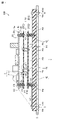
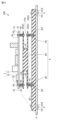
- Embodiment 5 Next, the configuration of electronic device 100 according to Embodiment 5 will be described with reference to FIGS. 29 to 34.
- FIG. The fifth embodiment has the same configuration and effects as those of the first embodiment unless otherwise specified. Therefore, the same reference numerals are given to the same configurations as in the above-described first embodiment, and description thereof will not be repeated.
- the fixing portion 5 is arranged so as to connect the housing 3 and the end surface 2c of the insulating plate 2 .
- first through portion H1 shown in FIG. 2 is not formed in insulating plate 2 .
- the fixing part 5 is composed of a fixture 5a and a fixture 5b.
- the shape of the fixture 5a is L-shaped.
- the fixture 5a has a first fixing portion 5a1 and a second fixing portion 5a2.
- the first fixing portion 5a1 is connected perpendicularly to the surface of the second fixing portion 5a2.
- a through hole 5ah is formed in each of the first fixing portion 5a1 and the second fixing portion 5a2.
- a plurality of horizontal holes 2h are formed in the end surface 2c of the insulating plate 2 in a side view of the insulating plate 2 viewed from the X direction in FIG.
- a plurality of through holes TH are formed outside the outer periphery of the insulating plate 2 when the housing 3 is viewed from the thickness direction of the housing 3 .
- Fixtures 5b are respectively inserted into the horizontal hole 2h and the through hole TH. In other words, the fixture 5b is inserted into the through hole 5ah and the horizontal hole 2h formed in the first fixing portion 5a1 so that the first fixing portion 5a1 is fixed to the end surface 2c, thereby connecting the first fixing portion 5a1 and the end surface 2c.
- the fixture 5b is inserted into the through hole 5ah and the through hole TH formed in the second fixing portion 5a2 so that the second fixing portion 5a2 is fixed to the housing 3, and the second fixing portion 5a2 and the housing are connected. to conclude.
- the creepage distance and the clearance distance are increased, so that the insulation performance is improved without increasing the size of the electronic device 100 .
- the number of fixtures 5a and fixtures 5b may be one or more.
- the through holes TH and the horizontal holes 2h may be formed such that the numbers of the through holes TH and the horizontal holes 2h match the numbers of the fixtures 5a.
- the through hole TH and the horizontal hole 2h are arranged so that the fixture 5a is connected to the side surface (end surface 2c) of the housing 3 and the insulating plate 2, respectively.
- the material of the fixture 5a may be, for example, a steel material such as steel or ferrous alloy.
- the material of the fixture 5a may be, for example, metals such as aluminum (Al) and copper (Cu), and non-ferrous metals such as alloys containing these.
- the material of the fixture 5a may be resin.
- the fixture 5b is configured by, for example, a screw.
- the screws are pan screws, for example, and are made of metal such as aluminum (Al), iron (Fe), stainless steel, and brass.
- the fixture 5b has conductivity.
- the fixture 5a does not have to connect the end surface 2c and the housing 3 using the fixture 5b.
- the fixture 5a, the end surface 2c and the housing 3 may be joined by welding.
- the creepage distance is the shortest distance f5 along the first surface 1a of the circuit board 1 between the conductive member 12 of the circuit board 1 and the first fixture F1, and the insulation between the circuit board 1 and the insulating plate 2. It is the sum of the shortest distance a5 along the surface of the support member 4 and the shortest distance g5 between the first engaging portion E1 and the fixing portion 5 along the surface of the insulating plate 2 (f5+a5+g5). Note that the shortest distance g5 between the first engaging portion E1 and the fixed portion 5 along the surface of the insulating plate 2 is the shortest distance g5 in the first embodiment because the fixed portion 5 is arranged on the end face 2c of the insulating plate 2. longer than the distance g1.
- the creepage distance (f5+a5+g5) of the present embodiment is the shortest creepage distance from the conductive member 12 of the circuit board 1 to the fixed portion 5 via the insulating support member 4 and the insulating plate 2.
- FIG. The creepage distance (f5+a5+g5) is designed to satisfy the creepage distance required by the standard.
- the spatial distance h5 is the sum of the shortest distance between the fixing portion 5 and the first fixture F1 and the shortest distance between the first fixture F1 and the conductive member 12 of the circuit board 1.
- the spatial distance h5 is longer than the spatial distance h5 in the first embodiment because the fixing portion 5 is arranged on the end surface 2c of the insulating plate 2. As shown in FIG.
- the creepage distance (f5+a5+g5) is longer than the clearance h5.
- the insulation performance (withstanding voltage value) of the electronic device 100 increases as the creepage distance (f5+a5+g5) increases. Therefore, the larger the in-plane dimension of the insulating plate 2, the longer the shortest distance g5 along the surface of the insulating plate 2 between the first engaging portion E1 and the fixing portion 5, so that the creeping distance (f5+a5+g5) becomes longer. Become. Therefore, as the in-plane dimension of the insulating plate 2 increases, the insulating performance (withstand voltage value) of the electronic device 100 improves.
- the creepage distance required for insulation between the circuit board 1 and the housing 3 is longer than the spatial distance required for insulation between the circuit board 1 and the housing 3 .
- the spatial distance required for insulation between the circuit board 1 and the housing 3 is h5
- the creepage distance required for insulation between the circuit board 1 and the housing 3 is (1.5 ⁇ h5).
- the creepage distance (f5+a5+g5) is (1.5 ⁇ h5) or more
- the circuit board 1 and the housing 3 are insulated.
- the fixture 5b is arranged on the end surface 2c, the creepage distance and the spatial distance are increased without increasing the size of the electronic device 100 in the thickness direction as compared with the first embodiment. That is, expansion of the thickness dimension and the in-plane dimension of the electronic device 100 is suppressed while ensuring both the creepage distance and the clearance distance between the circuit board 1 and the housing 3 and the insulation performance.
- the insulating support member 4 may have an insulator structure.
- the shortest distance a5 along the surface of the insulating support member 4 between the circuit board 1 and the insulating plate 2 is increased. Therefore, the creepage distance (f5+a5+g5) can be increased without increasing the dimension of the electronic device 100 in the thickness direction. Therefore, under the condition that the creepage distance is required to be longer than the spatial distance, it is possible to prevent the electronic device 100 from becoming excessively large in order to ensure the required insulation performance (creepage distance).
- insulating plate 2 has first insulating surface 2a and end surface 2c.
- the end surface 2c continues to the first insulating surface 2a.
- the fixing portion 5 connects the housing 3 and the end face 2c. Therefore, the creepage distance between the circuit board 1 and the fixing portion 5 can be further increased. Therefore, the withstand voltage value of the electronic device 100 can be further increased. Since the creepage distance and the spatial distance can be further increased, it is possible to further suppress the increase in the in-plane dimension of electronic device 100 .
- fixing portion 5 has first fixing portion 5a1 and second fixing portion 5a2.
- the first fixing portion 5a1 and the second fixing portion 5a2 are connected to each other.
- the first fixing portion 5a1 is fixed to the end surface 2c.
- the second fixing portion 5 a 2 is fixed to the housing 3 . Therefore, if the through holes 5ah are formed in the first fixing portion 5a1 and the second fixing portion 5a2, the housing 3 and the end surface 2c can be mechanically fastened using the fixture 5b.
Landscapes
- Engineering & Computer Science (AREA)
- Power Engineering (AREA)
- Microelectronics & Electronic Packaging (AREA)
- Mounting Of Printed Circuit Boards And The Like (AREA)
Priority Applications (1)
| Application Number | Priority Date | Filing Date | Title |
|---|---|---|---|
| JP2023551417A JP7550998B2 (ja) | 2021-09-30 | 2022-09-22 | 電子機器 |
Applications Claiming Priority (2)
| Application Number | Priority Date | Filing Date | Title |
|---|---|---|---|
| JP2021-161366 | 2021-09-30 | ||
| JP2021161366 | 2021-09-30 |
Publications (1)
| Publication Number | Publication Date |
|---|---|
| WO2023054179A1 true WO2023054179A1 (ja) | 2023-04-06 |
Family
ID=85782578
Family Applications (1)
| Application Number | Title | Priority Date | Filing Date |
|---|---|---|---|
| PCT/JP2022/035432 Ceased WO2023054179A1 (ja) | 2021-09-30 | 2022-09-22 | 電子機器 |
Country Status (2)
| Country | Link |
|---|---|
| JP (1) | JP7550998B2 (https=) |
| WO (1) | WO2023054179A1 (https=) |
Citations (3)
| Publication number | Priority date | Publication date | Assignee | Title |
|---|---|---|---|---|
| JPH01114796U (https=) * | 1988-01-27 | 1989-08-02 | ||
| JPH04219996A (ja) * | 1990-12-20 | 1992-08-11 | Matsushita Electric Works Ltd | 回路基板のケースへの収納構造 |
| US20170250010A1 (en) * | 2016-02-26 | 2017-08-31 | Delta Electronics, Inc. | Power supply |
-
2022
- 2022-09-22 WO PCT/JP2022/035432 patent/WO2023054179A1/ja not_active Ceased
- 2022-09-22 JP JP2023551417A patent/JP7550998B2/ja active Active
Patent Citations (3)
| Publication number | Priority date | Publication date | Assignee | Title |
|---|---|---|---|---|
| JPH01114796U (https=) * | 1988-01-27 | 1989-08-02 | ||
| JPH04219996A (ja) * | 1990-12-20 | 1992-08-11 | Matsushita Electric Works Ltd | 回路基板のケースへの収納構造 |
| US20170250010A1 (en) * | 2016-02-26 | 2017-08-31 | Delta Electronics, Inc. | Power supply |
Also Published As
| Publication number | Publication date |
|---|---|
| JP7550998B2 (ja) | 2024-09-13 |
| JPWO2023054179A1 (https=) | 2023-04-06 |
Similar Documents
| Publication | Publication Date | Title |
|---|---|---|
| US10297998B2 (en) | Electrical junction box | |
| US8922313B2 (en) | Induction device | |
| US8013709B2 (en) | Conductive module and assembly structure having such conductive module | |
| US12381337B2 (en) | Busbar connector | |
| US8120455B2 (en) | Transformer structure | |
| US10186363B2 (en) | Magnetic component unit | |
| JP2011155056A (ja) | シールド構造 | |
| JP4184179B2 (ja) | トランス及びそれを備えたトランスユニット | |
| JP7550998B2 (ja) | 電子機器 | |
| JP6317948B2 (ja) | トランスのコイル接続構造、及び、トランス | |
| US20090261938A1 (en) | Conductive module and transformer having such conductive module | |
| JP2013025974A (ja) | 電流補助部材 | |
| JPWO2019215922A1 (ja) | コネクタ | |
| JP6099135B2 (ja) | 電子機器、実装基板、及び実装基板の製造方法 | |
| JP5063672B2 (ja) | 配線基板及びその製造方法 | |
| TW202414456A (zh) | 用於高衝擊環境之表面貼裝相容平面磁體 | |
| JP7338434B2 (ja) | 電気装置 | |
| JP5992485B2 (ja) | 車載用dcdcコンバータ | |
| JP2011233824A (ja) | 電源装置および照明器具 | |
| JP2018190579A (ja) | 導電部材の接続構造およびそれを備える電動コンプレッサ | |
| JP7566122B2 (ja) | 電子機器 | |
| CN209804380U (zh) | 一种高压油箱的螺丝组件和具有其的高压油箱 | |
| CN101944425B (zh) | 磁性组件及其组装方法 | |
| JP7123236B2 (ja) | 回路基板 | |
| CN1516995A (zh) | 用于电子装置的电连接结构 |
Legal Events
| Date | Code | Title | Description |
|---|---|---|---|
| 121 | Ep: the epo has been informed by wipo that ep was designated in this application |
Ref document number: 22876046 Country of ref document: EP Kind code of ref document: A1 |
|
| WWE | Wipo information: entry into national phase |
Ref document number: 2023551417 Country of ref document: JP |
|
| NENP | Non-entry into the national phase |
Ref country code: DE |
|
| 122 | Ep: pct application non-entry in european phase |
Ref document number: 22876046 Country of ref document: EP Kind code of ref document: A1 |