WO2023053437A1 - イオンミリング装置 - Google Patents
イオンミリング装置 Download PDFInfo
- Publication number
- WO2023053437A1 WO2023053437A1 PCT/JP2021/036376 JP2021036376W WO2023053437A1 WO 2023053437 A1 WO2023053437 A1 WO 2023053437A1 JP 2021036376 W JP2021036376 W JP 2021036376W WO 2023053437 A1 WO2023053437 A1 WO 2023053437A1
- Authority
- WO
- WIPO (PCT)
- Prior art keywords
- rod
- ion
- source
- electrode
- ion source
- Prior art date
- Legal status (The legal status is an assumption and is not a legal conclusion. Google has not performed a legal analysis and makes no representation as to the accuracy of the status listed.)
- Ceased
Links
Images


Classifications
-
- H—ELECTRICITY
- H01—ELECTRIC ELEMENTS
- H01J—ELECTRIC DISCHARGE TUBES OR DISCHARGE LAMPS
- H01J37/00—Discharge tubes with provision for introducing objects or material to be exposed to the discharge, e.g. for the purpose of examination or processing thereof
- H01J37/02—Details
- H01J37/04—Arrangements of electrodes and associated parts for generating or controlling the discharge, e.g. electron-optical arrangement or ion-optical arrangement
- H01J37/08—Ion sources; Ion guns
-
- H—ELECTRICITY
- H01—ELECTRIC ELEMENTS
- H01J—ELECTRIC DISCHARGE TUBES OR DISCHARGE LAMPS
- H01J37/00—Discharge tubes with provision for introducing objects or material to be exposed to the discharge, e.g. for the purpose of examination or processing thereof
- H01J37/02—Details
-
- G—PHYSICS
- G01—MEASURING; TESTING
- G01N—INVESTIGATING OR ANALYSING MATERIALS BY DETERMINING THEIR CHEMICAL OR PHYSICAL PROPERTIES
- G01N1/00—Sampling; Preparing specimens for investigation
- G01N1/28—Preparing specimens for investigation including physical details of (bio-)chemical methods covered elsewhere, e.g. G01N33/50, C12Q
- G01N1/32—Polishing; Etching
-
- H—ELECTRICITY
- H01—ELECTRIC ELEMENTS
- H01J—ELECTRIC DISCHARGE TUBES OR DISCHARGE LAMPS
- H01J37/00—Discharge tubes with provision for introducing objects or material to be exposed to the discharge, e.g. for the purpose of examination or processing thereof
- H01J37/02—Details
- H01J37/20—Means for supporting or positioning the object or the material; Means for adjusting diaphragms or lenses associated with the support
-
- H—ELECTRICITY
- H01—ELECTRIC ELEMENTS
- H01J—ELECTRIC DISCHARGE TUBES OR DISCHARGE LAMPS
- H01J37/00—Discharge tubes with provision for introducing objects or material to be exposed to the discharge, e.g. for the purpose of examination or processing thereof
- H01J37/30—Electron-beam or ion-beam tubes for localised treatment of objects
- H01J37/305—Electron-beam or ion-beam tubes for localised treatment of objects for casting, melting, evaporating, or etching
- H01J37/3053—Electron-beam or ion-beam tubes for localised treatment of objects for casting, melting, evaporating, or etching for evaporating or etching
- H01J37/3056—Electron-beam or ion-beam tubes for localised treatment of objects for casting, melting, evaporating, or etching for evaporating or etching for microworking, e. g. etching of gratings or trimming of electrical components
-
- H—ELECTRICITY
- H01—ELECTRIC ELEMENTS
- H01J—ELECTRIC DISCHARGE TUBES OR DISCHARGE LAMPS
- H01J37/00—Discharge tubes with provision for introducing objects or material to be exposed to the discharge, e.g. for the purpose of examination or processing thereof
- H01J37/32—Gas-filled discharge tubes
- H01J37/32431—Constructional details of the reactor
- H01J37/32532—Electrodes
- H01J37/32568—Relative arrangement or disposition of electrodes; moving means
-
- H—ELECTRICITY
- H01—ELECTRIC ELEMENTS
- H01J—ELECTRIC DISCHARGE TUBES OR DISCHARGE LAMPS
- H01J2237/00—Discharge tubes exposing object to beam, e.g. for analysis treatment, etching, imaging
- H01J2237/30—Electron or ion beam tubes for processing objects
- H01J2237/317—Processing objects on a microscale
- H01J2237/31749—Focused ion beam
Definitions
- the present invention relates to an ion milling device.
- An ion milling apparatus irradiates an unfocused ion beam onto a sample (e.g., metal, semiconductor, glass, ceramic, etc.) to be observed with an electron microscope, and spatters atoms on the surface of the sample without stress by a sputtering phenomenon. It is used for polishing the sample surface and exposing the internal structure of the sample.
- the sample surface polished by the ion beam and the exposed internal structure of the sample are used for observation with a scanning electron microscope or a transmission electron microscope.
- a high voltage is applied between the anode and cathode inside the ion source to ionize the introduced gas with generated electrons, and an acceleration voltage is applied to extract the ions from the ion source and irradiate the sample.
- the cathode is worn by the sputtering phenomenon caused by the generated plasma, and a conductive deposited film derived from the composition of the cathode is formed on the inner wall surface of the anode.
- the deposited film grows with the lapse of operating time of the apparatus.
- the deposited film that has grown exfoliates like a needle and short-circuits between the anode and the cathode, making it impossible to generate ions. Therefore, it was necessary to disassemble the ion source and remove the short circuit. For this reason, in the conventional ion milling apparatus, it was necessary to interrupt sample processing and remove the deposited film every time a short circuit occurred.
- Cited Document 1 it is possible to remove the deposited film without decomposing the ion source by using the gas injection means. Pulling is required and processing efficiency is reduced.
- An ion milling apparatus which is an embodiment of the present invention, comprises a sample chamber, a sample stage disposed in the sample chamber on which the sample is placed, a first internal electrode, a second internal electrode, and an acceleration electrode. a source, a rod-shaped electrode that can be inserted into and removed from the ion source, and a power supply unit connected to the first internal electrode, the second internal electrode, the acceleration electrode, and the rod-shaped electrode, With the rod-shaped electrode retracted from the ion source, the power supply unit applies a first discharge voltage between the first internal electrode and the second internal electrode, and accelerates the voltage between the first internal electrode and the acceleration electrode.
- the ion source accelerates ions generated by collisions between the gas and electrons generated by the discharge between the first internal electrode and the second internal electrode, and accelerates them into the sample. emits as an unfocused beam of ions directed towards With the rod-shaped electrode inserted into the ion source, the power supply unit applies a second discharge voltage between the rod-shaped electrode and the first internal electrode and the second internal electrode, thereby causing the ion source to move inside. , ions are generated by collision of electrons generated by discharge between the rod-like electrode and the first internal electrode or the second internal electrode with the gas.
- An ion milling apparatus which is another embodiment of the present invention, includes a sample chamber, a sample stage disposed in the sample chamber on which the sample is placed, and electrons generated by discharge between an anode and a cathode.
- an ion source that accelerates ions with an acceleration electrode to emit them as an unfocused ion beam toward a sample;
- a power supply unit that is connected to the anode, the cathode, and the acceleration electrode;
- the discharge voltage applied between the anode and the cathode to the power supply unit and the difference between the anode and the accelerating electrode.
- a control unit stops application of an acceleration voltage applied between them, inserts a rod-shaped member into the ion source, and removes a short-circuited portion between the anode and the cathode with a brush.
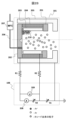
- FIG. 1 is a schematic diagram showing the main parts of an ion milling apparatus of Example 1.
- FIG. FIG. 4 is a diagram showing possible positional relationships between a shutter and an ion source;
- FIG. 4 is a diagram showing possible positional relationships between a shutter and an ion source;
- FIG. 2 is a schematic diagram showing an ion source and a power supply circuit that applies a control voltage to internal electrodes of the ion source;
- FIG. 2 is a schematic diagram showing an ion source and a power supply circuit that applies a control voltage to internal electrodes of the ion source; It is a schematic diagram which shows a mode that the shaft was inserted in the ion source.
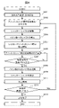
- FIG. 4 is a flow chart showing a series of operations from the start to end of sample processing of the ion milling apparatus of Example 1.
- FIG. FIG. 5 is a schematic diagram showing the main part of the ion milling apparatus of Example 2; 9 is a flow chart showing a series of operations from the start to end of sample processing of the ion milling apparatus of Example 2.
- FIG. 10 is a schematic diagram showing how a shaft with a brush is inserted into the ion source in the ion milling apparatus of Example 3; This is the shaft rotation source viewed from the Y direction. 10 is a flow chart showing a series of operations from the start to end of sample processing of the ion milling apparatus of Example 3.
- FIG. 5 is a schematic diagram showing the main part of the ion milling apparatus of Example 2; 9 is a flow chart showing a series of operations from the start to end of sample processing of the ion milling apparatus of Example 2.
- FIG. 10 is a schematic diagram showing how a shaft with a brush is
- a shutter 104 is provided in front of the ion source 101 to block irradiation of the sample with the ion beam.
- the direction in which the ion beam is emitted is called the front of the ion source, which corresponds to the Y direction in the example of FIG. 1A.
- a shutter drive source 105 drives the shutter 104 .
- FIGS. 1B shows a state in which the shaft 106 is retracted from the ion source 101 and the shutter 104 blocks the ion beam emitted from the ion source 101.
- FIG. FIG. 1C shows a state in which the shutter 104 is retracted from the front of the ion source 101 and the sample can be milled by the ion beam.
- FIG. 2A is a schematic diagram showing the ion source 101 adopting the Penning method and a power supply circuit that applies a control voltage to the internal electrodes of the ion source 101.
- the power supply circuit is part of the power supply unit 108 .
- the power supply circuit is equipped with an ammeter 208 and a voltmeter 209 between the anode 203 and the first cathode 201 and the second cathode 202 .
- the ammeter 208 measures the discharge current flowing between the cathode and the anode due to discharge
- the voltmeter 209 measures the discharge voltage actually applied between the cathode and the anode during discharge.
- a discharge current value measured by the ammeter 208 and a discharge voltage value measured by the voltmeter 209 are also output to the control unit 109 .
- the control unit 109 may use the discharge current value and the discharge voltage value to monitor the output state of the ion beam and display them on the display unit 110 .
- FIG. 2B shows the ion source 101 with the anode-cathode shorted. This short circuit eliminates the potential difference between the anode and the cathode and stops the discharge, thereby interrupting sample processing.
- FIG. 3 is a schematic diagram showing how the shaft 106 is inserted into the ion source 101 in order to remove the short circuit after the anode-cathode short circuit shown in FIG. 2B.
- the control unit 109 detects occurrence of a short circuit between the anode and the cathode, for example, when the discharge voltage value measured by the voltmeter 209 drops abnormally. Upon detection of the occurrence of the short circuit, the control unit 109 stops applying the control voltage to the ion source 101, moves the shutter 104 by the shutter drive source 105, and arranges the shaft 106 coaxially with the opening 211 of the acceleration electrode 205. do.
- the power supply unit 108 applies a high voltage (second discharge voltage) between the shaft 106 and the short-circuited cathodes 201, 202 and anode 203, thereby turning the ion source on.
- Argon gas introduced into 101 is ionized.
- the voltage Ve is a voltage value of negative polarity with respect to the reference potential
- the discharge voltage Vd and the acceleration voltage Va are set to 0 V so that a high voltage (second 2 discharge voltage) is applied and a discharge occurs.
- the shaft 106 functions as an anode
- the cathodes 201, 202 and 203 function as cathodes.
- the control unit 109 drives the shutter drive source 105 to move the shaft 106 forward of the ion source 101. At this time, the shaft 106 and the ion source 101 are arranged coaxially.
- the control unit 109 drives the shutter driving source 105 to retract the shaft 106 from the front of the ion source 101.
- step S311 If the anode-cathode short circuit occurs again during sample processing, the process returns to step S302 to remove the anode-cathode short circuit.
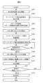
- FIG. 6 shows a series of operations from the start to end of sample processing of the ion milling apparatus 100B of the second embodiment.
- the same steps as those in the flowchart (FIG. 4) of the first embodiment are denoted by the same reference numerals, and overlapping descriptions are omitted.
- the control unit 109 drives the sample stage drive source 103 so that the shaft 106 and the ion source 101 are arranged coaxially. This operation changes the position and attitude of the sample stage 102 from the state before the interruption of processing. Therefore, the state information of the sample stage before being driven by the sample stage drive source 103 is recorded (S303').
- the state information is information for recovering the sample stage 102 to the state before the interruption of processing after short-circuit recovery, and includes the position coordinates (x, y, z) of the sample stage 102 and, if necessary, the posture of the sample stage 102. It contains information (tilt ⁇ 1 about T 1 axis, tilt ⁇ 2 about T 2 axis).
- FIG. 7A is a schematic diagram showing the ion source 101 of the ion milling apparatus of Example 3 and a power supply circuit that applies a control voltage to the internal electrodes of the ion source 101.
- FIG. The difference from Examples 1 and 2 is the method of removing the short-circuited portion between the anode and the cathode.
- a brush 401 is provided at the tip of a shaft (rod-shaped member) 106 , and the shaft 106 is attached to a shaft rotation source 402 via a shaft drive source 107 .
- the shaft 106 in Example 3 does not function as an external electrode and functions as a support member for the brush 401 .
- the shaft rotation source 402 viewed from the Y direction is shown in FIG. 7B.
- the shaft rotation source 402 rotates around the rotation center CC, and the shaft 106 rotates as the shaft rotation source 402 rotates.
- the shaft rotation source 402 is configured such that the holding positions of the shaft 106 and the shaft drive source 107 can be moved from the rotation center CC in the outer peripheral direction of the shaft rotation source 402 .
- Example 3 the controller 109 may stop the supply of argon gas to the ion source 101 .
- the control unit 109 drives the shutter drive source 105 to move the shaft 106 forward of the ion source 101 (S303).
- the shaft 106 is positioned at the rotation center CC of the shaft rotation source 402 so that the rotation center CC of the shaft rotation source 402 is arranged on the central axis of the ion source 101 .
- the shaft 106 and the ion source 101 are arranged coaxially.
Landscapes
- Chemical & Material Sciences (AREA)
- Analytical Chemistry (AREA)
- Physics & Mathematics (AREA)
- Plasma & Fusion (AREA)
- Engineering & Computer Science (AREA)
- General Health & Medical Sciences (AREA)
- Biochemistry (AREA)
- General Physics & Mathematics (AREA)
- Immunology (AREA)
- Pathology (AREA)
- Life Sciences & Earth Sciences (AREA)
- Health & Medical Sciences (AREA)
- Sampling And Sample Adjustment (AREA)
Priority Applications (4)
| Application Number | Priority Date | Filing Date | Title |
|---|---|---|---|
| JP2023550993A JP7672500B2 (ja) | 2021-10-01 | 2021-10-01 | イオンミリング装置 |
| KR1020247010458A KR102919596B1 (ko) | 2021-10-01 | 2021-10-01 | 이온 밀링 장치 |
| PCT/JP2021/036376 WO2023053437A1 (ja) | 2021-10-01 | 2021-10-01 | イオンミリング装置 |
| US18/696,487 US20250003841A1 (en) | 2021-10-01 | 2021-10-01 | Ion Milling Device |
Applications Claiming Priority (1)
| Application Number | Priority Date | Filing Date | Title |
|---|---|---|---|
| PCT/JP2021/036376 WO2023053437A1 (ja) | 2021-10-01 | 2021-10-01 | イオンミリング装置 |
Publications (1)
| Publication Number | Publication Date |
|---|---|
| WO2023053437A1 true WO2023053437A1 (ja) | 2023-04-06 |
Family
ID=85782043
Family Applications (1)
| Application Number | Title | Priority Date | Filing Date |
|---|---|---|---|
| PCT/JP2021/036376 Ceased WO2023053437A1 (ja) | 2021-10-01 | 2021-10-01 | イオンミリング装置 |
Country Status (4)
| Country | Link |
|---|---|
| US (1) | US20250003841A1 (https=) |
| JP (1) | JP7672500B2 (https=) |
| KR (1) | KR102919596B1 (https=) |
| WO (1) | WO2023053437A1 (https=) |
Citations (5)
| Publication number | Priority date | Publication date | Assignee | Title |
|---|---|---|---|---|
| JPH02148647A (ja) * | 1988-11-30 | 1990-06-07 | Nec Yamagata Ltd | イオン注入装置のイオンソース洗浄治具及び洗浄方法 |
| JPH0364462A (ja) * | 1989-07-31 | 1991-03-19 | Matsushita Electric Ind Co Ltd | イオンソースハウジング内壁のクリーニング方法およびクリーニング用治具 |
| CN202142496U (zh) * | 2011-07-25 | 2012-02-08 | 中芯国际集成电路制造(上海)有限公司 | 离子注入机的分析器 |
| WO2016189614A1 (ja) * | 2015-05-25 | 2016-12-01 | 株式会社日立ハイテクノロジーズ | イオンミリング装置、及びイオンミリング方法 |
| CN210207978U (zh) * | 2019-06-17 | 2020-03-31 | 德淮半导体有限公司 | 清洁装置及离子植入设备 |
Family Cites Families (1)
| Publication number | Priority date | Publication date | Assignee | Title |
|---|---|---|---|---|
| US7138629B2 (en) | 2003-04-22 | 2006-11-21 | Ebara Corporation | Testing apparatus using charged particles and device manufacturing method using the testing apparatus |
-
2021
- 2021-10-01 US US18/696,487 patent/US20250003841A1/en active Pending
- 2021-10-01 KR KR1020247010458A patent/KR102919596B1/ko active Active
- 2021-10-01 WO PCT/JP2021/036376 patent/WO2023053437A1/ja not_active Ceased
- 2021-10-01 JP JP2023550993A patent/JP7672500B2/ja active Active
Patent Citations (5)
| Publication number | Priority date | Publication date | Assignee | Title |
|---|---|---|---|---|
| JPH02148647A (ja) * | 1988-11-30 | 1990-06-07 | Nec Yamagata Ltd | イオン注入装置のイオンソース洗浄治具及び洗浄方法 |
| JPH0364462A (ja) * | 1989-07-31 | 1991-03-19 | Matsushita Electric Ind Co Ltd | イオンソースハウジング内壁のクリーニング方法およびクリーニング用治具 |
| CN202142496U (zh) * | 2011-07-25 | 2012-02-08 | 中芯国际集成电路制造(上海)有限公司 | 离子注入机的分析器 |
| WO2016189614A1 (ja) * | 2015-05-25 | 2016-12-01 | 株式会社日立ハイテクノロジーズ | イオンミリング装置、及びイオンミリング方法 |
| CN210207978U (zh) * | 2019-06-17 | 2020-03-31 | 德淮半导体有限公司 | 清洁装置及离子植入设备 |
Also Published As
| Publication number | Publication date |
|---|---|
| KR20240046301A (ko) | 2024-04-08 |
| US20250003841A1 (en) | 2025-01-02 |
| KR102919596B1 (ko) | 2026-01-29 |
| JP7672500B2 (ja) | 2025-05-07 |
| JPWO2023053437A1 (https=) | 2023-04-06 |
Similar Documents
| Publication | Publication Date | Title |
|---|---|---|
| US11742178B2 (en) | Ion milling device and milling processing method using same | |
| CN100497724C (zh) | 真空电弧沉积设备 | |
| KR20200115162A (ko) | 기판 처리 장치 및 탑재대의 제전 방법 | |
| EP2267181B1 (en) | Target exchange type plasma generator | |
| JP7332169B2 (ja) | 磁化プラズモイド射出装置 | |
| KR102371334B1 (ko) | 성막 방법 및 성막 장치 | |
| JP6499754B2 (ja) | イオンミリング装置、及びイオンミリング方法 | |
| JP7672500B2 (ja) | イオンミリング装置 | |
| JP2008209312A (ja) | 二次イオン質量分析装置及びその使用方法 | |
| US6610987B2 (en) | Apparatus and method of ion beam processing | |
| US10699876B2 (en) | Method of cleaning electrostatic chuck | |
| US9928998B2 (en) | Sputtering apparatus | |
| JP4827235B2 (ja) | アーク式蒸発源及び成膜体の製造方法 | |
| JP4448004B2 (ja) | 物品処理装置 | |
| JP2000251751A (ja) | 液体金属イオン源、および、液体金属イオン源のフローインピーダンス測定方法 | |
| JP2019218598A (ja) | 真空アーク蒸着装置および真空アーク蒸着方法 | |
| JP2007149861A (ja) | イオンミリング装置 | |
| US20240258062A1 (en) | Ion Milling Apparatus | |
| US20260038766A1 (en) | Ion Milling Device and Processing Method Using Same | |
| JP2010003596A (ja) | 荷電粒子線加工装置 | |
| TWI821868B (zh) | 離子銑削裝置 | |
| JP4774322B2 (ja) | 表面処理装置 | |
| JPH06325711A (ja) | スパッタ型イオン源 | |
| CN111640639A (zh) | 离子源及其清洁方法 | |
| JPH0828199B2 (ja) | 液体金属イオン源 |
Legal Events
| Date | Code | Title | Description |
|---|---|---|---|
| 121 | Ep: the epo has been informed by wipo that ep was designated in this application |
Ref document number: 21959471 Country of ref document: EP Kind code of ref document: A1 |
|
| ENP | Entry into the national phase |
Ref document number: 20247010458 Country of ref document: KR Kind code of ref document: A |
|
| WWE | Wipo information: entry into national phase |
Ref document number: 18696487 Country of ref document: US |
|
| WWE | Wipo information: entry into national phase |
Ref document number: 2023550993 Country of ref document: JP |
|
| NENP | Non-entry into the national phase |
Ref country code: DE |
|
| 122 | Ep: pct application non-entry in european phase |
Ref document number: 21959471 Country of ref document: EP Kind code of ref document: A1 |