WO2023053171A1 - プラズマ処理装置 - Google Patents
プラズマ処理装置 Download PDFInfo
- Publication number
- WO2023053171A1 WO2023053171A1 PCT/JP2021/035547 JP2021035547W WO2023053171A1 WO 2023053171 A1 WO2023053171 A1 WO 2023053171A1 JP 2021035547 W JP2021035547 W JP 2021035547W WO 2023053171 A1 WO2023053171 A1 WO 2023053171A1
- Authority
- WO
- WIPO (PCT)
- Prior art keywords
- cathode electrode
- hollow cathode
- plasma processing
- flat
- holder
- Prior art date
- Legal status (The legal status is an assumption and is not a legal conclusion. Google has not performed a legal analysis and makes no representation as to the accuracy of the status listed.)
- Ceased
Links
Images


Classifications
-
- H—ELECTRICITY
- H05—ELECTRIC TECHNIQUES NOT OTHERWISE PROVIDED FOR
- H05H—PLASMA TECHNIQUE; PRODUCTION OF ACCELERATED ELECTRICALLY-CHARGED PARTICLES OR OF NEUTRONS; PRODUCTION OR ACCELERATION OF NEUTRAL MOLECULAR OR ATOMIC BEAMS
- H05H1/00—Generating plasma; Handling plasma
- H05H1/24—Generating plasma
- H05H1/46—Generating plasma using applied electromagnetic fields, e.g. high frequency or microwave energy
Definitions
- the present invention relates to a plasma processing apparatus that uses plasma to perform plasma processing such as surface modification and film formation on an object to be processed.
- This type of plasma processing apparatus converts raw material gas introduced into a vacuum chamber into plasma by discharge from a cathode electrode, and performs plasma processing such as surface modification and film formation on an object to be processed.
- the present invention has been made in view of the above-mentioned problems, and is completely unheard of in the past in that not only can efficient and high-quality plasma processing be ensured, but it can also be easily applied to a wider range of applications.
- the aim is to provide a plasma processing apparatus.
- the plasma processing apparatus includes a holder that holds an object to be processed, and a hollow cathode electrode that is arranged opposite to the holder and has a bottomed hollow formed on a plasma generation surface that faces the holder. , a flat potential shield plate having a plurality of through holes formed therein, The potential shield plate is detachably attached at a predetermined distance from the plasma generation surface of the hollow cathode electrode, and the flat cathode electrode having a flat plasma generation surface can be replaced with the hollow cathode electrode. It is characterized by being configured to
- the type of plasma processing apparatus can be changed from the hollow cathode electrode type to the parallel plate electrode type by simply replacing the hollow cathode electrode and the flat plate cathode electrode by sharing the flow path of the raw material gas. Since it can be easily changed to any of the above, it becomes possible to easily cope with a wider range of uses.
- the potential shield plate can improve the quality of plasma processing, reduce power consumption, and shorten the cycle time.
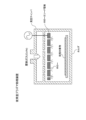
- FIG. 1 is a schematic cross-sectional view of a plasma processing apparatus in one embodiment of the present invention
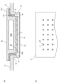
- FIG. FIG. 4A is a partial vertical cross-sectional view when the hollow cathode electrode is attached to the plasma processing apparatus according to the same embodiment
- FIG. 4B is a partial plan view of the hollow cathode electrode as viewed from below
- FIG. 4A is a partial vertical cross-sectional view when the flat cathode electrode is attached to the plasma processing apparatus of the same embodiment
- FIG. 4B is a partial plan view of the hollow cathode electrode as viewed from below.
- 1 is a schematic cross-sectional view of a conventional plasma processing apparatus;
- Plasma processing apparatus 1 Chamber 2: Hollow cathode electrode 2a: Plasma generation surface 2b: Back surface (anti-plasma generation surface) 3... Holder 41... Cooling body 8... Mounting structure 9... Potential shield plate 91... Through hole 10... Flat cathode electrode
- a plasma processing apparatus 100 as schematically shown in FIG. It comprises a cathode electrode 2 and a holder 3, a cooling mechanism 4 for cooling the hollow cathode electrode 2, and a power source 5 for applying a high frequency voltage to the hollow cathode electrode 2.
- a power source 5 for applying a high frequency voltage to the hollow cathode electrode 2.
- O 2 /Ar O 2 /Ar
- the chamber 1 is formed of a pair of opposing walls 11 and 12 and a side peripheral wall 13 therebetween and is made of metal and can be sealed.
- a hollow cathode electrode 2 is attached to one opposing wall 11
- the holder 3 is attached to the other opposing wall 12 .
- the side peripheral wall 13 is formed with a raw material gas introduction port (not shown) through which the raw material gas is introduced. In terms of potential, the vacuum chamber 1 is grounded.
- the hollow cathode electrode 2 is, for example, a rectangular plate of equal thickness.
- the plasma generation surface 2a which is one surface facing the holder 3 side, bottomed circular hole-shaped hollows 7 are regularly provided in a matrix, and the other surface 2b (hereinafter also referred to as the back surface 2b). ) is flat.
- the holder 3 has a pedestal shape, and a holding area for holding the object W to be processed is provided on the surface facing the hollow cathode electrode 2 .
- the cooling mechanism 4 includes a cooling body 41 made of metal, which is a conductor, and a pump or the like that circulates a coolant (here, liquid water) in a flow path 41 a formed inside the cooling body 41 .
- a mechanism 42 is provided.
- the cooling body 41 has, for example, a rectangular flat plate shape having a flange portion 411, and one surface 41b of the cooling body 41 has the same rectangular contour shape as that of the hollow cathode electrode 2. .
- a collar portion 411 of the cooling body 41 is attached to the opposing wall 11 so as to block an opening 11a provided in one opposing wall 11 of the vacuum chamber 1, and one side of the cooling body 41 is fitted into the opening 11 a so as to protrude into the vacuum chamber 1 .
- Reference numeral 6 in FIG. 2 denotes a rectangular annular insulator interposed between the cooling body 41 and the opposing wall 11 in order to electrically insulate the cooling body 41 from the vacuum chamber 1 .
- the back surface 2b of the hollow cathode electrode 2 is attached to one surface 41b of the cooling body 41 protruding into the vacuum chamber 1 in close contact with the predetermined attachment structure 8.
- the mounting structure 8 includes, for example, a plurality of screw holes (not shown) provided at a plurality of positions on one surface of the cooling body 41 and a plurality of screw insertion holes which are passed through corresponding positions of the hollow cathode electrode 2 .
- the hollow cathode electrode 2 is detachably attached to the cooling body 41 by fastening screws (not shown) via screws (not shown).
- the mounting structure 8 is not limited to this, and may be detachable using a clip or the like, for example.
- a potential shield plate 9 is arranged between the hollow cathode electrode 2 and the holder 3, as shown in FIGS.
- the potential shield plate 9 is, for example, a rectangular plate having the same thickness and is larger than the hollow cathode electrode 2, and is arranged so as to face the hollow cathode electrode 2 closely.
- a holder 14 is provided integrally protruding inward from the periphery of the opening 11a provided in the opposing wall 11.
- the peripheral portion of the potential shield plate 9 is detachably attached with screws or the like.
- the potential of the potential shield plate 9 is maintained at the same ground potential as that of the vacuum chamber 1 .
- the potential shield plate 9 is provided with through holes 91 having a diameter larger than that of the hollows 7 at positions coaxial with the hollows 7 of the hollow cathode electrode 2 . .
- the power supply 5 supplies high-frequency power to the hollow cathode electrode 2 through the cooling body 41 .
- the plasma processing apparatus 100 in this embodiment is provided with a flat cathode electrode 10 replaceable with the hollow cathode electrode 2, as shown in FIG.
- the flat cathode electrode 10 has a rectangular, equal-thickness flat plate shape having substantially the same shape as the hollow cathode electrode 2 in plan view, and the plasma generation surface 10a facing the holder 3 is flat.
- the flat cathode electrode 10 can be detachably attached to the cooling body 41 by a mounting structure 8 common to the hollow cathode electrode 2 .
- the flat cathode electrode 10 is provided with a screw insertion hole at the same position as the screw insertion hole of the hollow cathode electrode 2, and like the hollow cathode electrode 2, the screw hole is inserted into the screw hole of the cooling body 41.
- the back surface 10b of the flat plate cathode electrode 10 can be detachably attached to the end surface 41b of the cooling body 41 by tightening screws passed through the insertion holes.
- a raw material gas is introduced into the vacuum chamber 1 through a raw material gas introduction port (not shown) while the object W to be processed is placed on the holder 3 .
- an electric discharge occurs between the hollow cathode electrode 2 and the potential shield plate 9 , particularly in or near the hollow 7 of the hollow cathode electrode 2 , and the source gas becomes plasma. It reaches the object W to be processed through the hole 91 and modifies the surface of the object W to be processed.
- the flat cathode electrode 10 When the flat cathode electrode 10 is used, the hollow cathode electrode 2 and the potential shield plate 9 are removed, and the flat cathode electrode 10 is attached to one surface of the cooling body 41 as shown in FIG.
- the raw material gas is introduced into the vacuum chamber 1 from the raw material gas introduction port, and the power supply 5 is driven to generate the flat cathode electrode. 10 is supplied with high frequency power.
- glow discharge is generated between the flat cathode electrode 10 and the holder 3, and the material gas is turned into plasma to modify the surface of the object W to be processed.
- the material gas is turned into plasma to modify the surface of the object W to be processed.
- the type of plasma processing apparatus 100 can be easily changed to either a hollow cathode electrode type or a parallel plate electrode type with little change.
- the type of plasma processing apparatus 100 can be changed according to the processing purpose, and the range of applications is greatly expanded. From the manufacturer's point of view, two types of plasma processing apparatuses 100 can be manufactured simply by exchanging the electrodes, so that orders from users can be flexibly and quickly received, and costs can be reduced by using common parts.
- the potential shield plate 9 needs to be attached and detached when the electrodes are replaced.
- the potential shield plate 9 can be directly attached to the chamber 1 (the holder 14 integrally projecting from the chamber 1) with a screw or the like. No special wiring or the like is required.
- the cooling body 41 is in surface contact with all of the back surface 2b of the hollow cathode electrode 2 and the back surface 10b of the flat cathode electrode 10, these electrodes 2 and 10 can be uniformly cooled, and their thermal deformation is reduced. Efficient and high-quality plasma processing becomes possible by suppressing
- the potential shield plate 9 is interposed between the hollow cathode electrode 2 and the holder 3, the generation of parallel plate discharge (CCP) is suppressed, and the object W to be processed thereby is damaged. Temperature rise can be suppressed, and even if the processing object W is a plastic material, for example, the problem of deformation or melting can be avoided.
- CCP parallel plate discharge
- the table below shows the peel strength evaluation results when the hollow cathode electrode 2 was used to modify the surface of an ABS substrate, which is the object W to be processed, and a Cu film was formed thereon by sputtering.
- a comparison target is a plasma processing apparatus having a conventional hollow cathode electrode shown in FIG.
- the plasma processing apparatus 100 of the present embodiment can obtain approximately the same adhesion strength with less than half the electric power as compared with the conventional type, and can shorten the discharge time and cycle. It is also possible to shorten the time.
- the plasma processing apparatus 100 includes a holder 3 that holds an object W to be processed, and a hollow bottomed plasma generation surface 2a facing the holder 3 and facing the holder 3. 7 and a flat plate-shaped potential shield plate 9 having a plurality of through-holes 91 formed thereon and detachably mounted at a predetermined distance from the plasma generation surface 2a.
- a flat plate cathode electrode 10 having a flat plasma generation surface 2a is configured to be replaceable with the hollow cathode electrode 2 described above.
- the chamber 1 which accommodates the hollow cathode electrode 2 and the potential shield plate 9 and is set to a reference potential such as ground potential, is further provided.
- the cathode electrode 2 is attached to the chamber 1 via an insulating member, and the potential shield plate 9 is attached directly to the chamber 1 .
- a cooling body 41 to which the hollow cathode electrode 2 is attached to cool it is further provided, and the flat cathode electrode 10 is attached to the cooling body 41 . is attached so as to be replaceable with the hollow cathode electrode 2 .
- the mounting structure 8 of the hollow cathode electrode 2 to the cooling body 41 is replaced with the cooling mechanism 4. It is desirable to share the mounting structure 8 for the flat cathode electrode 10 .
- the cooling body 41 is made of a conductor and plasma discharge is performed. is preferably connected to the cathode electrodes 2 and 10 through the cooling body 41 .
- each cathode electrode is not limited to circular, but may be rectangular or polygonal.
- the shape of the cooling body can also be changed in various ways, and the cooling mechanism is not limited to the liquid-cooling type, but may be an air-cooling type or one using a refrigerating cycle. Alternatively, hot water may be used to adjust the temperature to about 70 degrees.
- the shape of the hollow may be any bottomed recess, such as a rectangular hole or groove.
- each cathode electrode to the cooling body and the attachment structure of the potential shield plate are not limited to the above embodiments.
- the holder and the potential shield plate may be set not only at the ground potential but also at other potentials, and the power source is not limited to the high frequency power source and may be a direct current power source.
- Plasma treatment is not limited to surface modification treatment, and may be film formation or etching.
- CH4 gas as a raw material gas for DLC film formation, or introduce Ar gas for etching.
- the present invention is not limited to the illustrated examples and explanations described above, and can be modified in various ways without departing from the spirit of the present invention.
- the type of plasma processing equipment can be easily changed between a hollow cathode electrode type and a parallel plate electrode type simply by exchanging the hollow cathode electrode and the flat plate cathode electrode, making it easy to handle a wider range of applications. become able to.
- the potential shield plate can improve the quality of plasma processing, reduce power consumption, and shorten the cycle time.
Landscapes
- Physics & Mathematics (AREA)
- Engineering & Computer Science (AREA)
- Plasma & Fusion (AREA)
- Electromagnetism (AREA)
- Spectroscopy & Molecular Physics (AREA)
- Chemical Vapour Deposition (AREA)
- Plasma Technology (AREA)
- Treatment Of Fiber Materials (AREA)
Priority Applications (4)
| Application Number | Priority Date | Filing Date | Title |
|---|---|---|---|
| JP2023550761A JP7512567B2 (ja) | 2021-09-28 | 2021-09-28 | プラズマ処理装置 |
| PCT/JP2021/035547 WO2023053171A1 (ja) | 2021-09-28 | 2021-09-28 | プラズマ処理装置 |
| CN202180097632.2A CN117204124A (zh) | 2021-09-28 | 2021-09-28 | 等离子体处理装置 |
| TW111114018A TWI834148B (zh) | 2021-09-28 | 2022-04-13 | 電漿處理裝置 |
Applications Claiming Priority (1)
| Application Number | Priority Date | Filing Date | Title |
|---|---|---|---|
| PCT/JP2021/035547 WO2023053171A1 (ja) | 2021-09-28 | 2021-09-28 | プラズマ処理装置 |
Publications (1)
| Publication Number | Publication Date |
|---|---|
| WO2023053171A1 true WO2023053171A1 (ja) | 2023-04-06 |
Family
ID=85781464
Family Applications (1)
| Application Number | Title | Priority Date | Filing Date |
|---|---|---|---|
| PCT/JP2021/035547 Ceased WO2023053171A1 (ja) | 2021-09-28 | 2021-09-28 | プラズマ処理装置 |
Country Status (4)
| Country | Link |
|---|---|
| JP (1) | JP7512567B2 (https=) |
| CN (1) | CN117204124A (https=) |
| TW (1) | TWI834148B (https=) |
| WO (1) | WO2023053171A1 (https=) |
Citations (6)
| Publication number | Priority date | Publication date | Assignee | Title |
|---|---|---|---|---|
| US4801839A (en) * | 1986-12-08 | 1989-01-31 | Applied Electron Corporation | Mounting of a cold cathode directly to a vacuum chamber wall |
| JPH0220325U (https=) * | 1988-07-25 | 1990-02-09 | ||
| JPH02215122A (ja) * | 1989-02-16 | 1990-08-28 | Fujitsu Ltd | ドライエッチング装置 |
| JP2008028087A (ja) * | 2006-07-20 | 2008-02-07 | Nisshinbo Ind Inc | プラズマエッチング電極 |
| JP2012054377A (ja) * | 2010-09-01 | 2012-03-15 | Toray Ind Inc | プラズマcvd装置 |
| JP2015086471A (ja) * | 2013-10-28 | 2015-05-07 | ベイパー テクノロジーズ、インコーポレイテッド | 低圧アーク・プラズマ浸漬被膜気相堆積及びイオン処理 |
Family Cites Families (8)
| Publication number | Priority date | Publication date | Assignee | Title |
|---|---|---|---|---|
| JP3113796B2 (ja) * | 1995-07-10 | 2000-12-04 | 東京エレクトロン株式会社 | プラズマ処理装置 |
| JP2001135626A (ja) * | 1999-11-02 | 2001-05-18 | Hitachi Kokusai Electric Inc | プラズマcvd装置及びプラズマcvd膜形成方法 |
| JP4493932B2 (ja) * | 2003-05-13 | 2010-06-30 | 東京エレクトロン株式会社 | 上部電極及びプラズマ処理装置 |
| KR101046335B1 (ko) * | 2008-07-29 | 2011-07-05 | 피에스케이 주식회사 | 할로우 캐소드 플라즈마 발생방법 및 할로우 캐소드플라즈마를 이용한 대면적 기판 처리방법 |
| JP5227239B2 (ja) * | 2009-04-13 | 2013-07-03 | 新明和工業株式会社 | ホローカソード型放電管 |
| JP6745643B2 (ja) * | 2016-05-17 | 2020-08-26 | 東京エレクトロン株式会社 | プラズマ処理装置およびプラズマ処理方法 |
| JP7246154B2 (ja) * | 2018-10-02 | 2023-03-27 | 東京エレクトロン株式会社 | プラズマ処理装置及び静電吸着方法 |
| JP7134863B2 (ja) * | 2018-12-27 | 2022-09-12 | 東京エレクトロン株式会社 | プラズマ処理装置およびプラズマ処理方法 |
-
2021
- 2021-09-28 CN CN202180097632.2A patent/CN117204124A/zh active Pending
- 2021-09-28 JP JP2023550761A patent/JP7512567B2/ja active Active
- 2021-09-28 WO PCT/JP2021/035547 patent/WO2023053171A1/ja not_active Ceased
-
2022
- 2022-04-13 TW TW111114018A patent/TWI834148B/zh active
Patent Citations (6)
| Publication number | Priority date | Publication date | Assignee | Title |
|---|---|---|---|---|
| US4801839A (en) * | 1986-12-08 | 1989-01-31 | Applied Electron Corporation | Mounting of a cold cathode directly to a vacuum chamber wall |
| JPH0220325U (https=) * | 1988-07-25 | 1990-02-09 | ||
| JPH02215122A (ja) * | 1989-02-16 | 1990-08-28 | Fujitsu Ltd | ドライエッチング装置 |
| JP2008028087A (ja) * | 2006-07-20 | 2008-02-07 | Nisshinbo Ind Inc | プラズマエッチング電極 |
| JP2012054377A (ja) * | 2010-09-01 | 2012-03-15 | Toray Ind Inc | プラズマcvd装置 |
| JP2015086471A (ja) * | 2013-10-28 | 2015-05-07 | ベイパー テクノロジーズ、インコーポレイテッド | 低圧アーク・プラズマ浸漬被膜気相堆積及びイオン処理 |
Also Published As
| Publication number | Publication date |
|---|---|
| JPWO2023053171A1 (https=) | 2023-04-06 |
| TW202315464A (zh) | 2023-04-01 |
| TWI834148B (zh) | 2024-03-01 |
| CN117204124A (zh) | 2023-12-08 |
| JP7512567B2 (ja) | 2024-07-09 |
Similar Documents
| Publication | Publication Date | Title |
|---|---|---|
| KR100757545B1 (ko) | 상부 전극 및 플라즈마 처리 장치 | |
| US8829387B2 (en) | Plasma processing apparatus having hollow electrode on periphery and plasma control method | |
| JP4102873B2 (ja) | プラズマ処理装置用電極板及びプラズマ処理装置 | |
| TW201931955A (zh) | 具有可拆卸高電阻率氣體分配板的噴淋頭 | |
| US20050248284A1 (en) | Fluid-cooled ion source | |
| JPH04297570A (ja) | 均一な消耗特性を持つ陰極装置 | |
| US10144040B2 (en) | Plasma processing method and plasma processing apparatus | |
| WO2023053171A1 (ja) | プラズマ処理装置 | |
| KR20190098918A (ko) | 피처리체의 탑재 장치 및 처리 장치 | |
| US20200035464A1 (en) | Cooling structure and parallel plate etching apparatus | |
| CN103403219A (zh) | 等离子体处理用磁控管电极 | |
| CN104928632A (zh) | 一种阴极电弧源 | |
| US20090218045A1 (en) | Plasma processing apparatus | |
| JP4456218B2 (ja) | プラズマ処理装置 | |
| KR101961596B1 (ko) | 스퍼터 타겟의 제조 방법 및 이를 수용하기 위한 스퍼터 건 | |
| JP4786731B2 (ja) | プラズマcvd装置 | |
| KR20080099046A (ko) | 유도 결합형 플라즈마 처리 장치 | |
| US20110039414A1 (en) | Plasma processing method and plasma processing apparatus | |
| TWI393797B (zh) | Sputtering electrodes and sputtering devices with sputtering electrodes | |
| JP2797111B2 (ja) | スパッタ装置 | |
| US6696672B2 (en) | Heating lamp brackets for reaction chambers of evaporation coating machines | |
| JP4619817B2 (ja) | 成膜装置用基板台、成膜装置及び成膜方法。 | |
| KR20210022113A (ko) | 캐소드용 아크 소스 시스템 | |
| JP2024105999A (ja) | 基板処理装置及び基板支持部 | |
| JPWO2023053171A5 (https=) |
Legal Events
| Date | Code | Title | Description |
|---|---|---|---|
| 121 | Ep: the epo has been informed by wipo that ep was designated in this application |
Ref document number: 21959224 Country of ref document: EP Kind code of ref document: A1 |
|
| WWE | Wipo information: entry into national phase |
Ref document number: 2023550761 Country of ref document: JP |
|
| WWE | Wipo information: entry into national phase |
Ref document number: 202180097632.2 Country of ref document: CN |
|
| NENP | Non-entry into the national phase |
Ref country code: DE |
|
| 122 | Ep: pct application non-entry in european phase |
Ref document number: 21959224 Country of ref document: EP Kind code of ref document: A1 |