WO2022270265A1 - アライナ装置 - Google Patents
アライナ装置 Download PDFInfo
- Publication number
- WO2022270265A1 WO2022270265A1 PCT/JP2022/022447 JP2022022447W WO2022270265A1 WO 2022270265 A1 WO2022270265 A1 WO 2022270265A1 JP 2022022447 W JP2022022447 W JP 2022022447W WO 2022270265 A1 WO2022270265 A1 WO 2022270265A1
- Authority
- WO
- WIPO (PCT)
- Prior art keywords
- wafer
- aligner
- light
- sensor
- edge
- Prior art date
- Legal status (The legal status is an assumption and is not a legal conclusion. Google has not performed a legal analysis and makes no representation as to the accuracy of the status listed.)
- Ceased
Links
Images


Classifications
-
- H—ELECTRICITY
- H10—SEMICONDUCTOR DEVICES; ELECTRIC SOLID-STATE DEVICES NOT OTHERWISE PROVIDED FOR
- H10P—GENERIC PROCESSES OR APPARATUS FOR THE MANUFACTURE OR TREATMENT OF DEVICES COVERED BY CLASS H10
- H10P72/00—Handling or holding of wafers, substrates or devices during manufacture or treatment thereof
- H10P72/50—Handling or holding of wafers, substrates or devices during manufacture or treatment thereof for positioning, orientation or alignment
- H10P72/53—Handling or holding of wafers, substrates or devices during manufacture or treatment thereof for positioning, orientation or alignment using optical controlling means
-
- B—PERFORMING OPERATIONS; TRANSPORTING
- B25—HAND TOOLS; PORTABLE POWER-DRIVEN TOOLS; MANIPULATORS
- B25J—MANIPULATORS; CHAMBERS PROVIDED WITH MANIPULATION DEVICES
- B25J9/00—Program-controlled manipulators
- B25J9/16—Program controls
- B25J9/1679—Program controls characterised by the tasks executed
- B25J9/1692—Calibration of manipulator
-
- H—ELECTRICITY
- H10—SEMICONDUCTOR DEVICES; ELECTRIC SOLID-STATE DEVICES NOT OTHERWISE PROVIDED FOR
- H10P—GENERIC PROCESSES OR APPARATUS FOR THE MANUFACTURE OR TREATMENT OF DEVICES COVERED BY CLASS H10
- H10P72/00—Handling or holding of wafers, substrates or devices during manufacture or treatment thereof
- H10P72/06—Apparatus for monitoring, sorting, marking, testing or measuring
- H10P72/0616—Monitoring of warpages, curvatures, damages, defects or the like
-
- H—ELECTRICITY
- H10—SEMICONDUCTOR DEVICES; ELECTRIC SOLID-STATE DEVICES NOT OTHERWISE PROVIDED FOR
- H10W—GENERIC PACKAGES, INTERCONNECTIONS, CONNECTORS OR OTHER CONSTRUCTIONAL DETAILS OF DEVICES COVERED BY CLASS H10
- H10W46/00—Marks applied to devices, e.g. for alignment or identification
-
- H—ELECTRICITY
- H10—SEMICONDUCTOR DEVICES; ELECTRIC SOLID-STATE DEVICES NOT OTHERWISE PROVIDED FOR
- H10W—GENERIC PACKAGES, INTERCONNECTIONS, CONNECTORS OR OTHER CONSTRUCTIONAL DETAILS OF DEVICES COVERED BY CLASS H10
- H10W46/00—Marks applied to devices, e.g. for alignment or identification
- H10W46/201—Marks applied to devices, e.g. for alignment or identification located on the periphery of wafers, e.g. orientation notches or lot numbers
-
- H—ELECTRICITY
- H10—SEMICONDUCTOR DEVICES; ELECTRIC SOLID-STATE DEVICES NOT OTHERWISE PROVIDED FOR
- H10W—GENERIC PACKAGES, INTERCONNECTIONS, CONNECTORS OR OTHER CONSTRUCTIONAL DETAILS OF DEVICES COVERED BY CLASS H10
- H10W46/00—Marks applied to devices, e.g. for alignment or identification
- H10W46/401—Marks applied to devices, e.g. for alignment or identification for identification or tracking
Definitions
- This application mainly relates to an aligner apparatus equipped with sensors for detecting wafer defects.
- Patent Document 1 Japanese Patent Application Laid-Open No. 2002-299419 discloses a multi-function wafer aligner.
- the multi-function wafer aligner performs wafer centering correction, wafer alignment, and wafer damage detection.
- a multi-function wafer aligner detects wafer damage using a light-emitting sensor and a light-receiving sensor.
- the light emission sensors are arranged side by side under the wafer and irradiate light upward.
- the light-receiving sensors are arranged side by side at a position facing the side surface of the wafer, and receive the light emitted by the light-emitting sensor and reflected by the wafer. Since there is a dent or the like at a portion where the wafer has a defect, the light is reflected in a different direction. Thereby, a wafer defect can be detected based on the position at which the light receiving sensor receives the light.
- Patent Document 2 International Publication No. 2019/165484 discloses an apparatus for inspecting wafers.
- a light emitting section and a detecting section are arranged so as to sandwich the wafer.
- the light emitting unit irradiates the edge of the wafer with laser light from a plurality of positions.
- the detector receives light reflected or scattered by the edge of the wafer.
- a wafer defect can be detected with high accuracy based on the detection result of the detection unit.
- the present application has been made in view of the above circumstances, and its main purpose is to provide an aligner apparatus that can detect wafer defects with high accuracy and shorten the time required for wafer inspection and alignment. to provide.
- an aligner device having the following configuration. That is, the aligner device includes a motor, a rotating device, a controller, and a sensor.
- the motor generates rotational driving force.
- the rotating device rotates while supporting the wafer by the rotational driving force generated by the motor.
- the control device controls the rotation of the rotating device to match the rotation phase of the wafer to a predetermined value.
- the sensor detects defects on the edge of the wafer by irradiating the edge of the wafer with a plurality of lights traveling in different directions and receiving the lights.
- wafer defects can be detected with high accuracy, and the time required for wafer inspection and alignment can be shortened.
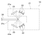
- FIG. 1 is a perspective view of an aligner device according to a first embodiment;
- 4 is a flowchart showing processing performed by a control device;
- the perspective view of the aligner apparatus which concerns on 2nd Embodiment.
- FIG. 1 is a perspective view of the aligner device 1 of the first embodiment.
- the aligner device 1 shown in FIG. 1 is arranged in a work space such as a clean room.
- a wafer 30 is transferred to the aligner device 1 by a robot (not shown).
- the robot is, for example, a SCARA type horizontal articulated robot.
- SCARA is an abbreviation for Selective Compliance Assembly Robot Arm.
- the wafer 30 is a circular thin plate-shaped semiconductor wafer.
- the wafer 30 may be a glass wafer instead of a semiconductor wafer.
- the aligner device 1 is a device that aligns the wafer 30 .
- Alignment is a process of acquiring the rotational phase of the wafer 30 and adjusting the rotational phase of the wafer 30 to a predetermined value.
- the rotational phase of the wafer 30 is the orientation of the wafer 30 that changes as the wafer 30 rotates.
- the two circular surfaces of the disk-shaped wafer 30 are referred to as main surfaces 31, and the surfaces connecting the main surfaces 31 are referred to as side surfaces 32.
- the radial end of the main surface 31 of the wafer 30 and the side surface 32 are collectively referred to as the edge of the wafer 30 .
- a notch 33 is formed at the edge of the wafer 30 .
- Notch 33 indicates the crystal orientation of the semiconductor. If an orientation flat is formed on the wafer 30 instead of the notch 33, the aligner apparatus 1 may be configured to detect the orientation flat. Further, the aligner device 1 may be configured to acquire the deviation of the center position of the wafer 30 with respect to the reference point in addition to the rotational phase of the wafer 30 .
- the aligner device 1 includes a rotating device 11 , a motor 12 , a control device 13 , a sensor 14 and a communication device 16 .
- the rotating device 11 is a disk-shaped rotating table.
- a wafer 30 is placed on the rotating device 11 by a robot.
- the rotating device 11 supports the wafer 30 by placing the wafer 30 thereon.
- the surface on which the wafer 30 is placed faces the vertical direction.
- the rotating device 11 is rotatably supported by a workbench or the like.
- the shape of the rotating device 11 is not limited to a disc.
- the rotating device 11 may have a rectangular plate shape.
- the rotating device 11 may be configured to support the wafer 30 by gripping the side surface of the wafer 30 .
- the motor 12 generates rotational driving force.
- a rotational driving force generated by the motor 12 is transmitted to the rotating device 11 .
- the rotating device 11 rotates around the vertical direction.
- the rotational phase of wafer 30 can be changed.
- the motor 12 is controlled by the control device 13.
- the control device 13 includes an arithmetic device such as a CPU, and a storage device such as an HDD, an SSD, or a flash memory.
- the arithmetic device controls the aligner device 1 by executing a program stored in the storage device.
- the control device 13 may control both the robot and the aligner device 1 or may control only the aligner device 1 .
- the rotating device 11 is provided with an unillustrated encoder. A detection result of the encoder is transmitted to the control device 13 . Thereby, the control device 13 can grasp the rotation phase of the rotation device 11 (that is, the rotation phase of the wafer 30).
- the sensor 14 inspects the wafer 30 placed on the rotating device 11 .
- the sensor 14 includes a housing 21 , a light projecting section 22 and a light receiving section 23 .
- the housing 21 is a box-shaped member that accommodates the members that make up the sensor 14 .
- the housing 21 is generally U-shaped and has a first portion 21a and a second portion 21b that are spaced apart and opposed.
- An inspection space 21c is formed between the first portion 21a and the second portion 21b.
- the edge of the wafer 30 supported by the rotating device 11 passes through the inspection space 21c. Accordingly, by rotating the rotating device 11 once, the edge of the wafer 30 can be inspected over the entire circumference.
- a plurality of light projecting sections 22 (specifically, three light projecting sections 22) and a light receiving section 23 are arranged in the first portion 21a.
- a plurality of light projecting units 22 (specifically, three light projecting units 22) and a light receiving unit 23 are arranged in the second portion 21b.
- the light projecting unit 22 is a laser generator, laser diode, SLD (super luminescent diode), or the like. Therefore, the light (laser light) emitted by the light projecting section 22 has directivity and a narrower spectrum width than the light emitted by the LED.
- Each light projection unit 22 irradiates light toward the edge of the wafer 30 .
- the optical axis of the light emitted by the light projecting unit 22 is in contact with the wafer 30 . Since the positions of the plurality of light projecting units 22 are different, the traveling direction of the light emitted by each light projecting unit 22 is different. Furthermore, the position of the contact point of the optical axis of light and the wafer 30 differs according to the light projecting section 22 .
- the light-receiving unit 23 receives the light emitted by the light-projecting unit 22 , generates a current signal (or a voltage signal converted from the current signal) according to the amount of received light, and outputs the current signal to the control device 13 .
- Light from the light projecting portion 22 arranged in the first portion 21a is received by the light receiving portion 23 arranged in the second portion 21b.
- the light from the light-projecting portion 22 arranged in the second portion 21b is received by the light-receiving portion 23 arranged in the first portion 21a.
- the control device 13 can distinguish from which light projecting part 22 the current signal input from the light receiving part 23 is caused by the light emitted.
- the light receiving section 23 includes a plurality of photodiodes, and each photodiode is arranged at a position overlapping the direction in which light from the light projecting section 22 travels. Accordingly, it is possible to identify the current signal caused by the light emitted by which light projecting unit 22 according to the photodiode that has output the current signal.
- the number of photodiodes constituting the light receiving section 23 may be one.
- the light projecting unit 22 emits light according to a predetermined schedule, and the light receiving unit 23 receives the light. Based on the time when the current signal is input and the schedule, the control device 13 can identify the current signal caused by the light emitted by which light projecting unit 22 .
- the light emitted by the light projecting unit 22 is received by the light receiving unit 23 after being affected by the surface of the edge of the wafer 30 (for example, after being diffracted by the surface). Therefore, if there is a defect on the surface of the edge of the wafer 30, the light received by the light receiving section 23 changes. Based on the current signal input from the light receiving section 23 , the control device 13 can identify whether or not there is a defect on the surface of the edge of the wafer 30 . As described above, the position of the contact point between the optical axis of the light emitted by the light projecting section 22 and the wafer 30 differs depending on the light projecting section 22 . Therefore, in this embodiment, defects can be inspected at a plurality of locations on the edge of the wafer 30 .
- the sensor 14 detects, for example, that the wafer 30 is warped, that the side surface 32 is uneven and has an inappropriate shape, that the amount of particles is greater than a predetermined value, that the diameter of the wafer is inappropriate, that the bonding Improper concentricity of multiple wafers (in the case of bonded wafers) can be detected.
- the wafer surface is irradiated with light perpendicularly as in Patent Document 1, it is difficult to detect particles existing on the wafer. Microparticles existing on the wafer 30 can be detected by irradiating with light.
- the control device 13 determines that there is a high possibility that the main surface 31 of the wafer 30 also has the same type of defect.
- the sensor 14 can also detect whether a notch 33 or an orientation flat is formed on the wafer 30 in the inspection space 21c.
- the notch 33 and orientation flats are pre-shaped.
- notches 33 and orientation flats are quite different in shape and size from common defects. Therefore, if the current signal output from the light receiving unit 23 when the notch 33 and the orientation flat are present is stored (learned) in advance in the controller 13, it is possible to determine whether there is a defect in the wafer 30 or not. It can be distinguished whether the wafer 30 has a notch 33 or an orientation flat. Thereby, the controller 13 can inspect the wafer 30 for defects and align the wafer 30 at the same time.
- the communication device 16 is either connected to the control device 13 or built into the control device 13 .
- the communication device 16 can communicate with the external device 40 .
- the external device 40 is a device higher than the aligner device 1 and collectively controls the aligner device 1 and other wafer processing devices.
- the communication device 16 is, for example, a communication module, and includes a connector for wired communication, an antenna for wireless communication, and the like.
- the control device 13 determines whether or not the wafer 30 is placed on the rotating device 11 (S101). This determination is made, for example, based on whether or not the control device 13 controls the robot to complete the work of placing the wafer 30 . If a control device other than the control device 13 controls the robot, the control device 13 may receive notification from the robot control device that the work of placing the wafer 30 on the rotating device 11 is completed.
- the control device 13 rotates the wafer 30 once by controlling the motor 12 to rotate the rotating device 11 (S102). Further, the controller 13 detects the edge defect and the notch 33 of the wafer 30 using the sensor 14 (S102). By measuring the edge of the wafer 30 with the sensor 14 while rotating the wafer 30 once, the defect of the wafer 30 can be inspected over the entire circumference. In addition, since the sensor 14 of the present embodiment detects edge defects and the notch 33 at the same time, the time required for inspection and alignment of the wafer 30 can be shortened.
- the control device 13 When the notch 33 is detected, the control device 13 records the position of the notch 33 based on the detected value of the encoder when the notch 33 is detected (S103). The position of notch 33 is recorded as the rotational phase of wafer 30 (rotator 11) when notch 33 is detected.
- the control device 13 transmits the detection result of the defect of the wafer 30 performed in step S102 to the external device 40 via the communication device 16 (S104).
- the defect detection result of the wafer 30 is transmitted in association with the identification information of the wafer 30 .
- the external device 40 determines whether or not the detection result of the defect of the wafer 30 is of a level that poses no problem as a product.
- the aligner device 1 may continue alignment when the external device 40 determines that there is no problem, or the aligner device 1 (control device 13) may align one or more wafers 30. After completion, external device 40 may make determinations for wafer 30 defects.
- the controller 13 adjusts the rotational phase of the wafer 30 to match the rotational phase of the wafer 30 with a predetermined value (S105). That is, the controller 13 controls the motor 12 to rotate the wafer 30 so that the position of the notch recorded in step S103 faces a predetermined direction.
- alignment and inspection of the wafer 30 can be performed by the same apparatus.
- the time required for processing the wafer 30 can be shortened compared to the case where the alignment and inspection of the wafer 30 are performed by separate apparatuses.
- the sensor 14 is configured to irradiate the wafer 30 with a plurality of lights traveling in different directions to detect defects of the wafer 30, various defects of the wafer 30 can be detected accurately.
- the sensor that detects defects in the wafer 30 and the sensor that detects the notch 33 in the wafer 30 are the same.
- the sensor for detecting defects in the wafer 30 and the sensor for detecting the notch 33 in the wafer 30 are separate.
- the sensor 14 equivalent to that of the first embodiment is used to detect defects in the wafer 30
- the line sensor 15 is used to detect the notch 33 of the wafer 30 .
- the line sensor 15 is a transmissive light amount measuring sensor.
- the line sensor 15 includes a light projecting portion 15a and a light receiving portion 15b.
- the light projecting section 15a emits light toward the light receiving section 15b.
- the cross section of the light emitted by the light projecting unit 15a is linear.
- a wafer 30 is arranged between the light projecting portion 15a and the light receiving portion 15b.
- the light receiving unit 15b receives light that is not blocked by the wafer 30 among the light emitted by the light projecting unit 15a.
- the light receiving unit 15 b generates a current signal (or a voltage signal obtained by converting the same) according to the amount of light received, and outputs the current signal to the control device 13 .
- the notch 33 exists between the light projecting portion 15a and the light receiving portion 15b, less light is blocked by the wafer 30, so the value of the current signal output from the light receiving portion 15b increases. Therefore, the notch 33 can specify the position (rotational phase) of the notch 33 based on the output value of the light receiving section 15b. If the center position of the wafer 30 is displaced, the value of the current signal output by the light receiving unit 15b constantly changes as the wafer 30 rotates. can be detected.
- the two functions performed by the sensor 14 are distributed to two sensors. This allows the function or setting of the sensor 14 to be specialized for detecting wafer 30 defects. As a result, there is a possibility that the detection accuracy of the defects of the wafer 30 can be further improved. It should be noted that the detection of defects in the wafer 30 and the control related to alignment are the same as in the first embodiment.
- the aligner device 1 of this embodiment includes the motor 12, the rotating device 11, the control device 13, and the sensor 14.
- the motor 12 generates rotational driving force.
- the rotating device 11 rotates while supporting the wafer 30 by the rotational driving force generated by the motor 12 .
- the control device 13 controls the rotation of the rotating device 11 to match the rotation phase of the wafer 30 to a predetermined value.
- the sensor 14 detects defects on the edge of the wafer 30 by irradiating the edge of the wafer 30 with a plurality of lights traveling in different directions and receiving the light.
- the aligner device 1 detects defects of the wafer 30 as well as alignment, the time required for inspection and alignment of the wafer 30 can be shortened.
- control device 13 rotates the wafer 30 at least once before matching the rotational phase of the wafer 30 to a predetermined value.
- Sensor 14 continues to detect edge defects of wafer 30 while controller 13 makes one revolution of wafer 30 .
- the wafer 30 can be inspected over its entire circumference.
- the controller 13 adjusts the rotational phase of the wafer 30 to a predetermined value based on the orientation flats or notches 33 formed in the wafer 30 .
- An orientation flat or notch 33 is detected using sensor 14 .
- the number of sensors can be reduced, so the cost of the aligner device can be reduced.
- the aligner device 1 of this embodiment includes a communication device 16 that communicates with an external device 40 .
- the communication device 16 associates the edge defect detection result of the wafer 30 with the identification information of the wafer 30 and transmits it to the external device 40 .
- the external device 40 can determine whether or not the defect detection result of the wafer 30 is at a level at which there is no problem as a product.
- the senor 14 detects defects on the side surface 32 of the wafer 30 without detecting defects on the main surface 31 of the wafer 30 .
- the controller 13 determines the defect of the main surface 31 of the wafer 30 based on the defect of the side surface 32 of the wafer 30 .
- the inspection time can be shortened compared to a configuration in which the entire main surface 31 of the wafer 30 is inspected.
- the light receiving section 23 receives the light emitted by the light projecting section 22 and received on the surface of the wafer 30 .
- the light receiving unit 23 may receive the light emitted by the light projecting unit 22 and reflected by the surface of the wafer 30 .
- the light projecting part 22 and the light receiving part 23 are arranged in the first part 21a, and the light projecting part 22 and the light receiving part 23 are arranged in the second part 21b.
- the light projecting section 22 may be arranged in the first portion 21a and the light receiving section 23 may be arranged in the second portion 21b (or vice versa).
- the flowchart shown in the above embodiment is an example, and some processes may be omitted, the contents of some processes may be changed, or new processes may be added.
- the process of detecting the defect of the wafer 30 and the notch 33 are performed simultaneously.
- the process of detecting the defects of the wafer 30 may be performed first, and then the process of detecting the notch 33 of the wafer 30 may be performed.
- the order of the processing in step S104 and the processing in step S105 may be changed.
- a processor is considered a processing circuit or circuit because it includes transistors and other circuits.
- a circuit, unit, or means is hardware that performs or is programmed to perform the recited functions.
- the hardware may be the hardware disclosed herein, or other known hardware programmed or configured to perform the functions recited.
- a circuit, means or unit is a combination of hardware and software, where the hardware is a processor which is considered a type of circuit, the software being used to configure the hardware and/or the processor.
Landscapes
- Engineering & Computer Science (AREA)
- Robotics (AREA)
- Mechanical Engineering (AREA)
- Container, Conveyance, Adherence, Positioning, Of Wafer (AREA)
- Investigating Materials By The Use Of Optical Means Adapted For Particular Applications (AREA)
Priority Applications (3)
| Application Number | Priority Date | Filing Date | Title |
|---|---|---|---|
| CN202280043607.0A CN117795656A (zh) | 2021-06-24 | 2022-06-02 | 对准装置 |
| JP2023529770A JP7832199B2 (ja) | 2021-06-24 | 2022-06-02 | アライナ装置 |
| KR1020247002815A KR102870970B1 (ko) | 2021-06-24 | 2022-06-02 | 얼라이너 장치 |
Applications Claiming Priority (2)
| Application Number | Priority Date | Filing Date | Title |
|---|---|---|---|
| US17/357,354 US12148646B2 (en) | 2021-06-24 | 2021-06-24 | Aligner apparatus |
| US17/357,354 | 2021-06-24 |
Publications (1)
| Publication Number | Publication Date |
|---|---|
| WO2022270265A1 true WO2022270265A1 (ja) | 2022-12-29 |
Family
ID=84541233
Family Applications (1)
| Application Number | Title | Priority Date | Filing Date |
|---|---|---|---|
| PCT/JP2022/022447 Ceased WO2022270265A1 (ja) | 2021-06-24 | 2022-06-02 | アライナ装置 |
Country Status (6)
| Country | Link |
|---|---|
| US (1) | US12148646B2 (https=) |
| JP (1) | JP7832199B2 (https=) |
| KR (1) | KR102870970B1 (https=) |
| CN (1) | CN117795656A (https=) |
| TW (1) | TWI843132B (https=) |
| WO (1) | WO2022270265A1 (https=) |
Cited By (1)
| Publication number | Priority date | Publication date | Assignee | Title |
|---|---|---|---|---|
| WO2026023488A1 (ja) * | 2024-07-26 | 2026-01-29 | 川崎重工業株式会社 | アライナ、ロボットシステム及び基板のアライメント方法 |
Families Citing this family (2)
| Publication number | Priority date | Publication date | Assignee | Title |
|---|---|---|---|---|
| US11521882B2 (en) * | 2020-08-20 | 2022-12-06 | Taiwan Semiconductor Manufacturing Company, Ltd. | Wafer notch positioning detection |
| TWM661429U (zh) * | 2024-08-05 | 2024-10-01 | 三和技研股份有限公司 | 晶圓定位裝置 |
Citations (4)
| Publication number | Priority date | Publication date | Assignee | Title |
|---|---|---|---|---|
| JP2006128423A (ja) * | 2004-10-29 | 2006-05-18 | Fujitsu Ltd | 半導体製造装置 |
| JP2008064595A (ja) * | 2006-09-07 | 2008-03-21 | Olympus Corp | 基板検査装置 |
| JP2009016438A (ja) * | 2007-07-02 | 2009-01-22 | Nitto Denko Corp | 半導体ウエハへの粘着テープ貼付け方法および保護テープの剥離方法 |
| JP2015195328A (ja) * | 2014-03-28 | 2015-11-05 | 株式会社ダイヘン | ワーク処理装置、ワーク搬送システム |
Family Cites Families (15)
| Publication number | Priority date | Publication date | Assignee | Title |
|---|---|---|---|---|
| US3560644A (en) * | 1968-02-29 | 1971-02-02 | Us Navy | Multiple projection television system |
| JP3074313B2 (ja) * | 1993-01-26 | 2000-08-07 | 株式会社メックス | ウエハーの位置決め装置 |
| KR100389129B1 (ko) | 2001-03-06 | 2003-06-25 | 삼성전자주식회사 | 멀티 펑션 웨이퍼 얼라이너 |
| US7968859B2 (en) * | 2003-07-28 | 2011-06-28 | Lsi Corporation | Wafer edge defect inspection using captured image analysis |
| KR20050120861A (ko) * | 2004-06-21 | 2005-12-26 | 삼성전자주식회사 | 프리 얼라이너를 이용한 웨이퍼 에지 검사 장치 및 그의검사 방법 |
| JP2006128440A (ja) * | 2004-10-29 | 2006-05-18 | Renesas Technology Corp | 半導体製造装置及び半導体装置の製造方法 |
| US7161667B2 (en) * | 2005-05-06 | 2007-01-09 | Kla-Tencor Technologies Corporation | Wafer edge inspection |
| JP5022793B2 (ja) * | 2007-07-02 | 2012-09-12 | 日東電工株式会社 | 半導体ウエハの欠陥位置検出方法 |
| US9076342B2 (en) * | 2008-02-19 | 2015-07-07 | Architecture Technology Corporation | Automated execution and evaluation of network-based training exercises |
| CN104407518B (zh) * | 2008-06-20 | 2017-05-31 | 因文西斯系统公司 | 对用于过程控制的实际和仿真设施进行交互的系统和方法 |
| WO2012134795A2 (en) * | 2011-03-25 | 2012-10-04 | Exxonmobile Upstream Research Company | Immersive training environment |
| US9886029B2 (en) * | 2013-12-02 | 2018-02-06 | Daihen Corporation | Workpiece processing apparatus and workpiece transfer system |
| AT520964B1 (de) | 2018-02-28 | 2019-11-15 | Tatiana Strapacova | Vorrichtung und Verfahren zur optischen Erfassung eines Randbereiches eines flachen Objektes |
| KR20190119803A (ko) * | 2018-04-13 | 2019-10-23 | 주식회사 넥서스원 | 웨이퍼의 에지 영역 검사장치 및 검사방법 |
| KR102134034B1 (ko) * | 2018-09-12 | 2020-07-14 | 블루테크코리아 주식회사 | 웨이퍼 치핑 검사 및 로봇 반복 정밀도 검사 가능한 얼라이너 및 상기 얼라이너에 의한 웨이퍼 치핑 검사방법 |
-
2021
- 2021-06-24 US US17/357,354 patent/US12148646B2/en active Active
-
2022
- 2022-06-02 CN CN202280043607.0A patent/CN117795656A/zh active Pending
- 2022-06-02 KR KR1020247002815A patent/KR102870970B1/ko active Active
- 2022-06-02 WO PCT/JP2022/022447 patent/WO2022270265A1/ja not_active Ceased
- 2022-06-02 JP JP2023529770A patent/JP7832199B2/ja active Active
- 2022-06-24 TW TW111123592A patent/TWI843132B/zh active
Patent Citations (4)
| Publication number | Priority date | Publication date | Assignee | Title |
|---|---|---|---|---|
| JP2006128423A (ja) * | 2004-10-29 | 2006-05-18 | Fujitsu Ltd | 半導体製造装置 |
| JP2008064595A (ja) * | 2006-09-07 | 2008-03-21 | Olympus Corp | 基板検査装置 |
| JP2009016438A (ja) * | 2007-07-02 | 2009-01-22 | Nitto Denko Corp | 半導体ウエハへの粘着テープ貼付け方法および保護テープの剥離方法 |
| JP2015195328A (ja) * | 2014-03-28 | 2015-11-05 | 株式会社ダイヘン | ワーク処理装置、ワーク搬送システム |
Cited By (1)
| Publication number | Priority date | Publication date | Assignee | Title |
|---|---|---|---|---|
| WO2026023488A1 (ja) * | 2024-07-26 | 2026-01-29 | 川崎重工業株式会社 | アライナ、ロボットシステム及び基板のアライメント方法 |
Also Published As
| Publication number | Publication date |
|---|---|
| TW202312339A (zh) | 2023-03-16 |
| JP7832199B2 (ja) | 2026-03-17 |
| KR20240041918A (ko) | 2024-04-01 |
| JPWO2022270265A1 (https=) | 2022-12-29 |
| CN117795656A (zh) | 2024-03-29 |
| US20220415690A1 (en) | 2022-12-29 |
| KR102870970B1 (ko) | 2025-10-14 |
| US12148646B2 (en) | 2024-11-19 |
| TWI843132B (zh) | 2024-05-21 |
Similar Documents
| Publication | Publication Date | Title |
|---|---|---|
| WO2022270265A1 (ja) | アライナ装置 | |
| US7723710B2 (en) | System and method including a prealigner | |
| US12044627B2 (en) | Defect inspection device and defect inspection method | |
| JP4681607B2 (ja) | 回転デバイス上の半導体基板の位置検出装置及び方法 | |
| TW201611174A (zh) | 晶圓之位置檢測裝置、晶圓之位置檢測方法及記憶媒體 | |
| TWI823237B (zh) | 對準裝置及對準方法 | |
| KR20220152963A (ko) | 웨이퍼 가공 방법 및 시스템 | |
| CN102788769A (zh) | 晶圆检测装置及使用其的晶圆检测方法 | |
| US11428645B2 (en) | Wafer inspection device and method of manufacturing semiconductor device by using the wafer inspection device | |
| CN111220904A (zh) | 测试互连基板的方法和用于执行该方法的装置 | |
| US20070002316A1 (en) | Wafer aligner, semiconductor manufacturing equipment, and method for detecting particles on a wafer | |
| KR100675558B1 (ko) | 웨이퍼의 직경을 측정할 수 있는 장치 및 방법 | |
| KR100953341B1 (ko) | 반도체 제조용 웨이퍼 검사장치 | |
| JP2007165655A (ja) | ウエハ方向センサー | |
| KR20080008443A (ko) | 반도체 코팅설비의 웨이퍼 플랫존 정렬상태 검출장치 | |
| JP2010117323A (ja) | 表面検査装置 | |
| JP4018899B2 (ja) | 基板処理ユニット、基板処理装置及び基板処理方法 | |
| KR102326680B1 (ko) | 소재 물성 검사 장치 | |
| TW202238071A (zh) | 平行度檢測方法及平行度檢測裝置 | |
| TW202449964A (zh) | 用於原位驗證和校正晶圓位置的方法和系統 | |
| JP2662524B2 (ja) | X線分析における試料の方位の判定方法および装置 | |
| TW201248138A (en) | Wafer inspection device and wafer inspection method using the same | |
| KR20060069991A (ko) | 웨이퍼 정렬 방법 및 웨이퍼 정렬 장치 | |
| KR20040069764A (ko) | 반도체 웨이퍼에 코팅된 감광막 표면의 검사장치 | |
| KR20070002265A (ko) | 오버레이 측정 장치 및 방법 |
Legal Events
| Date | Code | Title | Description |
|---|---|---|---|
| 121 | Ep: the epo has been informed by wipo that ep was designated in this application |
Ref document number: 22828183 Country of ref document: EP Kind code of ref document: A1 |
|
| WWE | Wipo information: entry into national phase |
Ref document number: 2023529770 Country of ref document: JP |
|
| WWE | Wipo information: entry into national phase |
Ref document number: 202280043607.0 Country of ref document: CN |
|
| WWE | Wipo information: entry into national phase |
Ref document number: 1020247002815 Country of ref document: KR |
|
| NENP | Non-entry into the national phase |
Ref country code: DE |
|
| 122 | Ep: pct application non-entry in european phase |
Ref document number: 22828183 Country of ref document: EP Kind code of ref document: A1 |