WO2022269809A1 - シリアル通信システム - Google Patents
シリアル通信システム Download PDFInfo
- Publication number
- WO2022269809A1 WO2022269809A1 PCT/JP2021/023813 JP2021023813W WO2022269809A1 WO 2022269809 A1 WO2022269809 A1 WO 2022269809A1 JP 2021023813 W JP2021023813 W JP 2021023813W WO 2022269809 A1 WO2022269809 A1 WO 2022269809A1
- Authority
- WO
- WIPO (PCT)
- Prior art keywords
- control circuit
- information
- circuit unit
- main control
- communication
- Prior art date
- Legal status (The legal status is an assumption and is not a legal conclusion. Google has not performed a legal analysis and makes no representation as to the accuracy of the status listed.)
- Ceased
Links
Images


Classifications
-
- B—PERFORMING OPERATIONS; TRANSPORTING
- B60—VEHICLES IN GENERAL
- B60R—VEHICLES, VEHICLE FITTINGS, OR VEHICLE PARTS, NOT OTHERWISE PROVIDED FOR
- B60R16/00—Electric or fluid circuits specially adapted for vehicles and not otherwise provided for; Arrangement of elements of electric or fluid circuits specially adapted for vehicles and not otherwise provided for
- B60R16/02—Electric or fluid circuits specially adapted for vehicles and not otherwise provided for; Arrangement of elements of electric or fluid circuits specially adapted for vehicles and not otherwise provided for electric constitutive elements
-
- G—PHYSICS
- G05—CONTROLLING; REGULATING
- G05B—CONTROL OR REGULATING SYSTEMS IN GENERAL; FUNCTIONAL ELEMENTS OF SUCH SYSTEMS; MONITORING OR TESTING ARRANGEMENTS FOR SUCH SYSTEMS OR ELEMENTS
- G05B23/00—Testing or monitoring of control systems or parts thereof
- G05B23/02—Electric testing or monitoring
-
- H—ELECTRICITY
- H04—ELECTRIC COMMUNICATION TECHNIQUE
- H04L—TRANSMISSION OF DIGITAL INFORMATION, e.g. TELEGRAPHIC COMMUNICATION
- H04L25/00—Baseband systems
- H04L25/02—Details ; arrangements for supplying electrical power along data transmission lines
-
- H—ELECTRICITY
- H04—ELECTRIC COMMUNICATION TECHNIQUE
- H04L—TRANSMISSION OF DIGITAL INFORMATION, e.g. TELEGRAPHIC COMMUNICATION
- H04L5/00—Arrangements affording multiple use of the transmission path
- H04L5/14—Two-way operation using the same type of signal, i.e. duplex
Definitions
- the present disclosure relates to a full-duplex serial communication system that simultaneously transmits and receives downstream communication information from the main control circuit unit to the monitoring control circuit unit and upstream communication information from the monitoring control circuit unit to the main control circuit unit.
- a supervisory control circuit section is provided to constantly monitor whether the microprocessor is operating normally, and the supervisory control circuit section serves as the main control circuit section for the microprocessor. and the microprocessor returns answer information to the question information to the supervisory control circuit section. It is known to use a so-called Q&A abnormality determination means for confirming whether an answer has been obtained (Patent Document 1).
- An aspect of the present disclosure is intended to solve the above problems, and an object thereof is to provide a serial communication system capable of transmitting and receiving data more frequently.
- a serial communication system performs full-duplex communication in which downstream communication information and upstream communication information are simultaneously transmitted and received based on a main control circuit unit, a communication permission signal, and a communication synchronization signal.
- a pair of serial interface circuits constituting a heavy block communication circuit and a pair of serial interface circuits are connected to the main control circuit unit, and periodically and sequentially transmit inquiry information for the main control circuit unit to the main control circuit unit, a monitoring control circuit unit that compares answer information from the main control circuit unit based on question information with correct answer information and determines whether or not there is an abnormality in the main control circuit unit.
- the communication permission signal is a signal that is periodically transmitted from the main control circuit section to the monitoring control circuit section through the first control signal line and permits the monitoring control circuit section to start full-duplex communication.
- the communication synchronizing signal is transmitted from the monitoring control circuit unit to the main control circuit unit or from the main control circuit unit to the monitoring control circuit unit through the second control signal line. pulse.
- the downstream communication information is transmitted from the main control circuit unit to the supervisory control circuit unit by downstream communication, and contains the first setting constant required by the supervisory control circuit unit and the query information obtained from the previous upstream communication information. Contains answer information and code check information.
- the upstream communication information is transmitted from the monitoring control circuit unit to the main control circuit unit by upstream communication, and includes a second setting constant corresponding to the first setting constant obtained from the main control circuit unit, and current question information. and code checking information.
- the first set constant includes a variable first variable set constant and a fixed first fixed set constant.
- the supervisory control circuit unit stores the first fixed setting constant included in the downstream communication information in the memory.
- the supervisory control circuit unit sends upstream communication information including second set constants including the first fixed set constants stored in the memory, current question information, and code check information to the main control circuit unit. to send.
- the main control circuit unit supplies the monitoring control circuit unit with the first setting constant including the first variable setting constant excluding the first fixed setting constant and the previous upstream communication information. forwarding communication information including answer information and code check information for the received question information;
- a serial communication system can transmit and receive more frequently.
- FIG. 1 is a diagram illustrating the configuration of an electronic device based on Embodiment 1;
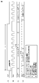
- FIG. It is a figure explaining the time chart explaining the serial communication of the electronic device in a comparative example.
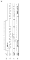
- 4 is a diagram explaining a time chart of the serial communication system according to the first embodiment;
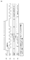
- FIG. FIG. 10 is a diagram explaining a time chart of a serial communication system according to a second embodiment;
- FIG. 10 is a diagram explaining a time chart of a serial communication system according to a third embodiment;
- FIG. 1 is a diagram illustrating the configuration of an electronic device based on Embodiment 1.
- electronic equipment 10A includes a main control circuit section 20A composed mainly of a microprocessor 20 and a monitoring control circuit section 30A composed mainly of a logic circuit section 39. As shown in FIG.
- the electronic device 10A is configured to operate by receiving power from an external power supply 13, which is an in-vehicle battery.
- the input sensor group 11B connected to the outside of the electronic device 10A is composed of, for example, switches and analog sensors.
- the electric load group 12B driven by the electronic device 10A is composed of relays.
- the external tool 19 is connected to the electronic device 10A via a detachable connector (not shown) at the time of product shipment or maintenance and inspection, and communicates with the microprocessor 20 via the tool interface circuit 29 to control the program memory 25A, which will be described later. It is used to transfer and write programs and control constants.
- the main control circuit section 20A is mainly composed of a 32-bit microprocessor 20.
- the microprocessor 20 includes a program memory 25A, which is, for example, a non-volatile flash memory, and an arithmetic processing is configured to cooperate with the RAM memory 24 of the
- the program memory 25A stores a communication control program in addition to the input/output control program.
- the monitoring control circuit section 30A is mainly composed of a logic circuit section 39 constituted by, for example, a gate array.
- a memory (DMEM) 35A is configured to cooperate with a multi-channel AD converter 36 for the analog sensors in the input sensor group 11B.
- the input interface circuit 31 is connected between the input sensor group 11B and the input port of the logic circuit section 39, and is composed of a low-pass filter for converting signal voltage levels and suppressing signal noise.
- the output interface circuit 32 is connected between the electrical load group 12B and the output port of the logic circuit section 39, and is composed of power transistors for driving various electrical loads.
- the logic circuit section 39 performs communication control of input/output signals by hardware.
- the power supply circuit 33 is supplied with power from the external power supply 13, generates a stabilized voltage such as DC 5 [V] or DC 3.3 [V], and controls the main control circuit section 20A, the monitoring control circuit section 30A, and each input/output interface circuit. is configured to power the
- serial interface circuits 27A, 37A constituted by a pair of serial-to-parallel converters form a full-duplex block communication circuit.
- Upstream communication information UPD from 30A to main control circuit section 20A can be simultaneously transmitted and received.
- the communication permission signal ALT generated by the main control circuit section 20A and the communication synchronization signal CLK generated by the monitoring control circuit section 30A will be described later with reference to FIG.
- the direct memory access controller 27B is connected between the parallel input/output bus of the serial-to-parallel conversion circuit that constitutes the serial interface circuit 27A and the data bus of the microprocessor 20. It is for sending and receiving data between
- the upstream communication storage information 28 is received data stored in the RAM memory 24 by upstream communication, and includes question information for Q&A, input signal information obtained from the input sensor group 11B, set information, monitoring total information, flag/ There is tag information and code check information.
- the downstream communication storage information 38 is received data stored in the RAM memory 34 by downstream communication, and includes answer information for Q&A, setting information such as control constants required by the monitoring control circuit unit 30A, and information for the electric load group 12B. There are output signal information, flag/tag information, and code check information.
- the set information in the upstream communication storage information 28 is the same information as the setting information and the output signal information stored in the RAM memory 34 as the downstream communication information.
- the main control circuit unit 20A side can confirm whether or not the setting information and the output signal information are correctly transmitted.
- Correct answer information corresponding to question information is stored in the data memory 35A of the monitoring control circuit section 30A in advance at the stage of product shipment.
- the logic circuit unit 39 randomly transmits question information to the main control circuit unit 20A, and compares the answer information returned from the microprocessor 20 with the correct answer information stored in advance, thereby controlling the operation of the microprocessor 20. Monitor status.
- the microprocessor 20 of the main control circuit section 20A is configured to try to reply to the monitor control circuit section 30A with an intentional wrong answer and to reverse monitor whether the monitor control circuit section 30A is performing proper monitoring control. It is
- the monitor control circuit unit 30A detects an abnormality in the main control circuit unit 20A
- the main control circuit unit 20A is initialized and restarted by the reset output RST2, and the main control circuit unit 20A resumes the monitor control circuit unit.
- the monitor control circuit section 30A is initialized and restarted by a reset output RST1.
- the watchdog timer 40 monitors a watchdog signal WD, which is a pulse train generated by the microprocessor 20 of the main control circuit section 20A, and when the pulse width exceeds a reference value, generates a reset pulse RST to restart the main control circuit section. 20A and the monitor control circuit unit 30A are initialized and restarted.
- the data memory 35A for storing the correct answer information may be composed of a ROM memory determined by the wiring pattern among the integrated circuit elements constituting the monitoring control circuit section 30A instead of the EEPROM memory.
- the real values in the input data table specified by the question information are back-calculated to obtain answer information that matches the correct answer information fixedly stored in advance, and the back-calculated values are stored in the program memory 25A. You should keep it.
- the data memory 35A stores the correct answer information in advance. It is possible to determine whether or not the information matches.
- FIG. 2 is a diagram explaining a time chart explaining serial communication of an electronic device in a comparative example.
- a communication permission signal ALT shown in (A) of FIG. 2 is periodically transmitted from the main control circuit section 20A to the monitoring control circuit section 30A through an independent control signal line, and the main control circuit section 20A performs full-duplex block communication. It is a signal for permitting the start.
- the communication permission signal ALT in the first embodiment is an alternating signal whose logic level changes when communication is permitted.
- the communication synchronization signal CLK shown in FIG. 2B is transmitted from the monitoring control circuit section 30A to the main control circuit section 20A through an independent control signal line, and the number of pulses corresponding to at least the number of bits of communication information is transmitted. configured to occur.
- This communication synchronizing signal CLK is a pulse train signal in which the serial communication signal starts to be generated after a predetermined waiting time ⁇ has passed after the monitoring control circuit unit 30A receives the communication permission signal ALT.
- This communication synchronizing signal CLK stops pulse generation after generating a predetermined number of pulses corresponding to the number of transmission and reception bits, or continues pulse generation even after completing the generation of the predetermined amount of pulses.
- the pulse generation is temporarily stopped, and after a waiting time ⁇ , the pulse generation is restarted.
- ALT occurs early, the generation of the remaining pulses is omitted, and the pulse generation is started again after waiting time ⁇ .
- the upstream communication information UPD shown in FIG. 2C includes report information, which is input signal information to the monitor control circuit section 30A, or set constants or control output storage information obtained from the main control circuit section 20A, and this It includes question information and code check information, and has a data length of, for example, 500 bits.
- the downstream communication information DND shown in (D) of FIG. 2 is transmitted from the main control circuit section 20A to the monitoring control circuit section 30A, and is command information that is a set constant or a control output required in the monitoring control circuit section 30A. , and includes answer information and code check information for question information obtained in the previous upstream communication information UPD, and has a data length of, for example, 100 bits.
- the communication synchronization signal CLK must generate at least 500 pulses. While the communication period T0 of the communication permission signal ALT is, for example, 5 [msec], the time required to transmit and receive 500-bit data is, for example, 0.5 [msec].
- the waiting time ⁇ is a time of several 100 [ ⁇ sec]. During this waiting time ⁇ , an AD conversion command is generated for the multi-channel AD converter 36, and AD conversion of all channels is completed. It is configured.
- the question information included in the upstream communication information UPD is such that the same question information is transmitted during an extended period (question update period) Tq (for example, 40 [msec]) during which the communication permission signal ALT permits communication a plurality of times. It is configured.
- the flag changes at the same time
- the answer information included in the downstream communication information DND is configured so that the answer information corresponding to the question information is transmitted and the flag changes at the same time.
- an 8-bit first tag is added to the downstream communication information DND, and is a serial number or random number varying between 0 and 255.
- FIG. For example, when numerical data 255 is added as the first tag to downstream communication information DND, the monitoring control circuit unit 30A receiving this adds the same numerical data 255 as the second tag in the next upstream communication information UPD. configured to add
- the main control circuit section 20A and the supervisory control circuit section 30A are controlled each time. The same data will be received in the downstream communication, and it will not be possible to determine whether or not proper reception is being performed. On the other hand, if the first and second tag information are added, it is possible to confirm that new data has been received by checking that at least the tag information has changed in the received data each time.
- the control circuit section 20A is configured to be able to confirm that the monitoring control circuit section 30A is receiving proper data.
- the command information is information relating to control of the constituent elements of the monitoring control circuit section 30A, for example, information for starting AD conversion.
- the setting constants are changed during operation, and some are fixed by the electronic control unit and are not changed during operation.
- the main control circuit section 20A and the monitoring control circuit section 30A communicate the same data each time.
- the fixed setting constant is a setting for switching the input voltage range of the input sensor group 11B. For example, there are those that operate with an input voltage range of 0 to 2V and those that operate with an input voltage range of 0 to 5V.
- the report information which is the stored information of the control output, includes numerical information and abnormality information.
- Numerical information is AD conversion information, for example.
- the abnormality information is, for example, failure information of an analog sensor.
- the main control circuit unit 20A adds code check information to the downstream communication information DND, and the supervisory control circuit unit 30A checks whether or not an abnormality such as mixing or missing of bit information has occurred by sum check or CRC check. . Similarly, the supervisory control circuit unit 30A adds code check information to the upstream communication information UPD, and the supervisory control circuit unit 30A checks.
- FIG. 1 when power is connected to the electronic device 10A through a power switch (not shown), the microprocessor 20 responds to the operating state of the input sensor group 11B and the content of the control program in the program memory 25A. Drive control of the electric load group 12B is performed.
- the input sensor group 11B and the electric load group 12B do not perform high-frequency operation, it is necessary to quickly perform signal communication when the operating state changes. It is a thing.
- the main control circuit unit 20A at the time of activation, sends command information, which is a set constant or a control output required by the monitoring control circuit unit 30A, to the monitoring control circuit unit 30A as the downstream communication information DND. , the answer information and the code check information to the question information obtained in the previous uplink communication information UPD are transmitted.
- the monitoring control circuit section 30A stores fixed setting constants among the setting constants transmitted from the main control circuit section 20A in the data memory 35A.
- the supervisory control circuit section 30A supplies the main control circuit section 20A with Q&A question information, input signal information obtained from the input sensor group 11B, set information, supervisory aggregate information, flag/ Transmit tag information and code check information.
- the main control circuit section 20A supplies the monitoring control circuit section 30A with command information, which is a setting constant or a control output required by the monitoring control circuit section 30A, as downstream communication information DND. , and transmit the answer information and the code check information to the question information obtained in the previous upstream communication information UPD.
- command information which is a setting constant or a control output required by the monitoring control circuit section 30A
- the main control circuit unit 20A uses, as downstream communication information DND, setting constants including variable setting constants excluding fixed setting constants, and answer information and codes for question information obtained in the previous upstream communication information.
- Send downstream communication information including inspection information.
- FIG. 3 is a diagram explaining a time chart of the serial communication system according to the first embodiment.
- the fixed setting constant indicated by information K in FIG. 2 is removed from the upstream communication information UPD shown in (C), and The fixed setting constant indicated by the information K in FIG. 2 is also removed from the communication information DND.
- the amount of data in the downlink communication information DND and the uplink communication information UPD can be reduced, so that the communication cycle T1 can be made shorter than the communication cycle T0 in FIG.
- the main control circuit unit 20A stores the downlink communication information DND including fixed setting constants in the data memory 35A.
- the monitoring control circuit unit 30A transmits setting information using fixed setting constants stored in the data memory 35A.
- the main control circuit unit 20A receives the setting completion information and confirms that the fixed setting constant is stored in the data memory 35A of the monitoring control circuit unit 30A.
- the main control circuit unit 20A does not include fixed setting constants in the downstream communication information DND from the next time onwards.
- the amount of data in the downlink communication information DND can be reduced, so that the overall communication volume can be reduced and the communication cycle can be shortened.
- the downstream communication information DND and the upstream communication information UPD are exchanged as in the method of the comparative example shown in FIG.
- the downstream communication information DND and the upstream communication information UPD are exchanged with the information K removed from the UPD. This makes it possible to shorten the communication cycle T1 from the next time onward.
- the main control circuit unit 20A when the main control circuit unit 20A is first activated, the main control circuit unit 20A transmits a fixed setting constant to the monitoring control circuit unit 30A.
- a scheme for exchanging DND and upstream communication information UPD has been described.
- the fixed setting constant indicated by the removed information K is stored in advance in the data memory 35A constituting the monitoring control circuit section 30A, and is read out and used when the power supply of the monitoring control circuit section 30A is turned on. good too.
- FIG. 4 is a diagram explaining a time chart of the serial communication system according to the second embodiment.
- variable setting constant indicated by information J in FIG. 2 and the fixed setting constant indicated by information K are removed from the upstream communication information UPD shown in (C), and instead , information S indicating that the current information (J+K) and the previous information (J+K) shown by S in FIG. 4 match each other.
- the set information of the upstream communication information UPD is the same information as the setting information and the output signal information stored in the RAM memory 34 as the downstream communication information.
- the main control circuit section 20A confirms whether or not the setting information and the output signal information from the circuit section 30A are correctly transmitted.
- the monitor control circuit unit 30A compares the setting information stored in the RAM memory 34 as the previous downlink communication information with the setting information transmitted as the current downlink communication information.
- the monitoring control circuit unit 30A transmits information S indicating a match instead of the information (J+K) that is the set information of the upstream communication information UPD.
- the monitor control circuit unit 30A transmits information S indicating mismatch if the comparison result is not the same, instead of the information (J+K) that is the set information of the upstream communication information UPD.
- the main control circuit section 20A can confirm whether or not the setting information has been changed in the monitoring control circuit section 30A.
- the main control circuit unit 20A confirms that the current information (J+K) and the previous information (J+K) match with the information S, and if the setting constant is changed, It is confirmed by the information S that the current information (J+K) and the previous information (J+K) do not match.
- the communication cycle T2 can be made shorter than the communication cycle T0 in FIG.
- FIG. 5 is a diagram explaining a time chart of the serial communication system according to the third embodiment.
- report information that is numerical information indicated by information L in FIG. Information is removed, and instead, information indicating whether information L or information M is included is added to the current uplink communication information UPD indicated by information T in FIG.
- the communication cycle T3 can be made shorter than the communication cycle T0 in FIG.
- this is effective only when the main control circuit unit 20A satisfies the control requirements if there is information L or information M to be reported. For example, when information L is used for normal control and information M is used to detect an abnormality, the main control circuit unit 20A is reset.
- the report information of the upstream communication information UPD includes numerical information and anomaly information.
- Numerical information is AD conversion information, for example. This is 10-bit numerical information indicating the input voltage when the input voltage range is set to 0.1V to 4.9V.
- the anomaly information is, for example, a ground short anomaly when the input voltage range is less than 0.1 V, and a power short anomaly when the input voltage range is greater than 4.9 V.
- the monitor control circuit unit 30A transmits AD conversion information as numerical information in upstream communication information UPD together with information T indicating normal times.
- the monitoring and control circuit unit 30A transmits information T indicating that there is an abnormality and information indicating that there is a ground short-circuit abnormality or a power supply short-circuit abnormality in the upstream communication information UPD.
- the main control circuit unit 20A acquires the abnormality information or numerical information indicated by the information M according to the information T.
- the main control circuit unit 20A executes abnormality processing according to the information T if there is an abnormality, and executes control based on the notification information if there is no abnormality.
- communication cycle T3 can be made shorter than communication cycle T0 in FIG.
- the configuration illustrated as the above-described embodiment is an example of the configuration of the present disclosure, and can be combined with another known technique. , can also be modified and configured. Further, in the above-described embodiment, the processing and configuration described in other embodiments may be appropriately adopted and implemented.
Landscapes
- Engineering & Computer Science (AREA)
- Signal Processing (AREA)
- Computer Networks & Wireless Communication (AREA)
- Mechanical Engineering (AREA)
- Physics & Mathematics (AREA)
- General Physics & Mathematics (AREA)
- Automation & Control Theory (AREA)
- Power Engineering (AREA)
- Dc Digital Transmission (AREA)
- Communication Control (AREA)
Abstract
シリアル通信システムは、主制御回路部と、通信許可信号と通信同期信号とに基づいて、下り通信情報と上り通信情報とを同時に送受信する全二重通信を行う全二重ブロック通信回路を構成する一対のシリアルインタフェース回路と、一対のシリアルインタフェース回路を介して主制御回路部と接続され、主制御回路部に対する質問情報を定期的に主制御回路部へ順次送信し、質問情報に基づく主制御回路部からの回答情報と正解情報とを比較して主制御回路部の異常の有無を判定する監視制御回路部とを備える。起動時において、監視制御回路部は、下り通信情報に含まれる第1の固定設定定数をメモリに格納する。監視制御回路部は、主制御回路部に対して、メモリに格納された第1の固定設定定数とを含む第2の設定定数と、今回の質問情報と、符号点検情報とを含む上り通信情報を送信する。主制御回路部は、起動時の後、監視制御回路部に対して、第1の固定設定定数を除いた第1の可変設定定数を含む第1の設定定数と、前回の上り通信情報で得られた質問情報に対する回答情報と符号点検情報とを含む下り通信情報を送信する。
Description
本開示は、主制御回路部から監視制御回路部に対する下り通信情報と、監視制御回路部から主制御回路部に対する上り通信情報とを同時に送受信する全二重シリアル通信システムに関する。
マイクロプロセッサを搭載した電子機器において、当該マイクロプロセッサが正常に動作しているかどうかを常時監視するために監視制御回路部を設けて、当該監視制御回路部が主制御回路部となるマイクロプロセッサに対して質問情報を送信し、マイクロプロセッサがこの質問情報に対する回答情報を監視制御回路部へ返信し、監視制御回路部は返信された回答情報と予め提供されている正解情報とを比較して正常な回答が得られたかどうかを確認する、いわゆるQ&A方式の異常判定手段を用いることが知られている(特許文献1)。
一方で、より高頻度に送受信するためにさらなる改善が求められる。
本開示のある局面は、上記の課題を解決するためのものであって、より高頻度に送受信することが可能なシリアル通信システムを提供することを目的とする。
本開示のある局面は、上記の課題を解決するためのものであって、より高頻度に送受信することが可能なシリアル通信システムを提供することを目的とする。
ある実施の形態に従うと、シリアル通信システムは、主制御回路部と、通信許可信号と通信同期信号とに基づいて、下り通信情報と上り通信情報とを同時に送受信する全二重通信を行う全二重ブロック通信回路を構成する一対のシリアルインタフェース回路と、一対のシリアルインタフェース回路を介して主制御回路部と接続され、主制御回路部に対する質問情報を定期的に主制御回路部へ順次送信し、質問情報に基づく主制御回路部からの回答情報と正解情報とを比較して主制御回路部の異常の有無を判定する監視制御回路部とを備える。通信許可信号は、第1の制御信号線によって主制御回路部から監視制御回路部に対して定期的に送信され、監視制御回路部に対して全二重通信の開始を許可する信号である。通信同期信号は、第2の制御信号線によって、監視制御回路部から主制御回路部、又は主制御回路部から監視制御回路部に対して送信されて、少なくとも通信情報のビット数に応じた数のパルスを発生する。下り通信情報は、主制御回路部から監視制御回路部への下り通信により送信されて、監視制御回路部において必要とされる第1の設定定数、前回の上り通信情報で得られた質問情報に対する回答情報と符号点検情報とを含む。上り通信情報は、監視制御回路部から主制御回路部への上り通信により送信されて、主制御回路部から得られた第1の設定定数に対応する第2の設定定数と、今回の質問情報と符号点検情報とを含む。第1の設定定数は、可変の第1の可変設定定数と、固定の第1の固定設定定数とを含む。起動時において、監視制御回路部は、下り通信情報に含まれる第1の固定設定定数をメモリに格納する。監視制御回路部は、主制御回路部に対して、メモリに格納された第1の固定設定定数とを含む第2の設定定数と、今回の質問情報と、符号点検情報とを含む上り通信情報を送信する。主制御回路部は、起動時の後、監視制御回路部に対して、第1の固定設定定数を除いた第1の可変設定定数を含む第1の設定定数と、前回の上り通信情報で得られた質問情報に対する回答情報と符号点検情報とを含む下り通信情報を送信する。
本開示に従うシリアル通信システムは、より高頻度に送受信することが可能である。
以下、実施形態について図に基づいて説明する。以下の説明では、同一部品には、同一の符号を付している。それらの名称および機能も同じであるためそれらについての詳細な説明は繰り返さない。
実施の形態1.
図1は、実施の形態1に基づく電子機器の構成について説明する図である。図1を参照して、電子機器10Aは、マイクロプロセッサ20を主体として構成された主制御回路部20Aと、論理回路部39を主体として構成された監視制御回路部30Aを含む。
図1は、実施の形態1に基づく電子機器の構成について説明する図である。図1を参照して、電子機器10Aは、マイクロプロセッサ20を主体として構成された主制御回路部20Aと、論理回路部39を主体として構成された監視制御回路部30Aを含む。
電子機器10Aは、車載バッテリである外部電源13から給電されて動作するように構成されている。
電子機器10Aの外部に接続されている入力センサ群11Bは、例えば、スイッチやアナログセンサによって構成されている。
電子機器10Aによって駆動される電気負荷群12Bは、リレーによって構成されている。
外部ツール19は、製品出荷時又は保守点検時に電子機器10Aに対して図示しない脱着コネクタを介して接続され、ツールインタフェース回路29を介してマイクロプロセッサ20と交信することによって後述のプログラムメモリ25Aに制御プログラムや制御定数を転送書込みするためのものである。
次に、電子機器10Aの内部の構成として、主制御回路部20Aは、32ビットのマイクロプロセッサ20を主体として構成され、このマイクロプロセッサ20は、例えば不揮発フラッシュメモリであるプログラムメモリ25Aと演算処理用のRAMメモリ24と協働するように構成されている。
なお、プログラムメモリ25Aには、入出力制御プログラムに加えて、通信制御プログラムが格納されている。
監視制御回路部30Aは、例えばゲートアレーによって構成された論理回路部39を主体として構成されており、この論理回路部39は、演算処理用のRAMメモリ(RMEM)34、不揮発EEPROMメモリ等によるデータメモリ(DMEM)35A、入力センサ群11Bの中のアナログセンサに対する多チャンネルAD変換器36と協働するように構成されている。
入力インタフェース回路31は、入力センサ群11Bと論理回路部39の入力ポート間に接続され、信号電圧レベルの変換や信号ノイズを抑制するためのローパスフィルタにより構成されている。
出力インタフェース回路32は、電気負荷群12Bと論理回路部39の出力ポート間に接続され、各種電気負荷を駆動するためのパワートランジスタによって構成されている。なお、論理回路部39は、入出力信号の通信制御をハードウエアにより行なうものである。
電源回路33は、外部電源13から給電されて、DC5[V]、DC3.3[V]等の安定化電圧を生成し、主制御回路部20Aや監視制御回路部30A及び各入出力インタフェース回路に給電するように構成されている。
一対の直並列変換器によって構成されたシリアルインタフェース回路27A、37Aは、全二重ブロック通信回路を構成し、主制御回路部20Aから監視制御回路部30Aに対する下り通信情報DNDと、監視制御回路部30Aから主制御回路部20Aに対する上り通信情報UPDとを同時に送受信することができるように構成されている。
主制御回路部20Aが発生する通信許可信号ALTと、監視制御回路部30Aが発生する通信同期信号CLKについては図2により後述する。
ダイレクトメモリアクセスコントローラ27Bは、シリアルインタフェース回路27Aを構成する直並列変換回路の並列入出力バスとマイクロプロセッサ20のデータバス間に接続されて、マイクロプロセッサ20を経由しないで演算処理用RAMメモリ24との間のデータの授受を行なうためのものである。
上り通信格納情報28は、上り通信によってRAMメモリ24に格納される受信データであり、Q&A用の質問情報、入力センサ群11Bから得られた入力信号情報、設定済情報、監視集計情報、フラグ/タグ情報、符号点検情報がある。
下り通信格納情報38は、下り通信によってRAMメモリ34に格納される受信データであり、Q&A用の回答情報、監視制御回路部30Aで必要とされる制御定数などの設定情報、電気負荷群12Bに対する出力信号情報、フラグ/タグ情報、符号点検情報がある。
上り通信格納情報28の中の設定済情報とは、下り通信情報としてRAMメモリ34に格納された設定情報と出力信号情報と同一の情報であり、この設定済情報によって、監視制御回路部30Aからの設定情報と出力信号情報とが正しく送信されているか否かを、主制御回路部20A側で確認することができるように構成されている。
監視制御回路部30Aのデータメモリ35Aには、質問情報に対応した正解情報が製品出荷段階で予め格納されている。論理回路部39は、ランダムに質問情報を主制御回路部20Aに送信し、マイクロプロセッサ20から返信された回答情報と、予め格納されている正解情報とを比較することによって、マイクロプロセッサ20の動作状態を監視する。
主制御回路部20Aのマイクロプロセッサ20は、意図的な誤答を監視制御回路部30Aへ回答してみて、監視制御回路部30Aが適正な監視制御を行なっているかどうかを逆監視するように構成されている。
前述の動作の結果、監視制御回路部30Aが主制御回路部20Aの異常を検出すると、リセット出力RST2によって主制御回路部20Aを初期化して再起動し、主制御回路部20Aが監視制御回路部30Aの異常を検出するとリセット出力RST1によって監視制御回路部30Aを初期化して再起動するように構成されている。
ウォッチドッグタイマ40は、主制御回路部20Aのマイクロプロセッサ20が発生するパルス列であるウォッチドッグ信号WDを監視して、そのパルス幅が基準値を超過するとリセットパルスRSTを発生して主制御回路部20Aと監視制御回路部30Aを初期化して再起動するように構成されている。
正解情報を格納しておくデータメモリ35Aは、EEPROMメモリに代えて、監視制御回路部30Aを構成する集積回路素子の中で、配線パターンによって決定されるROMメモリにより構成してもよい。この場合、質問情報によって指定される入力データテーブル内の実数値は、予め固定記憶された正解情報と合致する回答情報が得られるような値を逆算して、この逆算値をプログラムメモリ25Aに格納しておけばよい。なお、本例においては、データメモリ35Aは、正解情報を予め格納する場合について説明するが、質問情報から所定の演算方式により正解情報を導出できるのであれば、正解情報を格納しなくても回答情報と合致するか否かを判断することが可能である。
次に、比較例における電子機器におけるシリアル通信について説明する。
図2は、比較例における電子機器のシリアル通信を説明するタイムチャートについて説明する図である。
図2は、比較例における電子機器のシリアル通信を説明するタイムチャートについて説明する図である。
図2の(A)に示す通信許可信号ALTは、独立した制御信号線によって主制御回路部20Aから監視制御回路部30Aに対して定期送信され、主制御回路部20Aが全二重ブロック通信の開始を許可するための信号である。この実施の形態1における通信許可信号ALTは、通信許可時点で論理レベルが変化する交番信号となっている。
従って、交番信号の論理レベルが変化する都度、新たな通信ブロックの送信開始が許可されることになるが、一定論理レベルが維持されているときには、所定ビット数の通信が完了すると今回の通信は完了し、所定ビット数の通信が完了する前に論理レベルが反転すると通信データの中断処理が行なわれるように構成されている。
図2の(B)に示す通信同期信号CLKは、独立した制御信号線によって監視制御回路部30Aから主制御回路部20Aに対して送信され、少なくとも通信情報のビット数に応じた数のパルスを発生するように構成されている。この通信同期信号CLKは、監視制御回路部30Aが通信許可信号ALTを受信してから所定の待機時間τの経過後に発生を開始して、シリアル通信信号が歩進移動するパルス列信号である。
この通信同期信号CLKは、送受信ビット数に対応した所定量のパルス数を発生してからパルス発生を停止するか、又は所定量のパルスの発生を完了しても尚パルス発生を持続して、次回の通信許可信号ALTの発生に伴ってパルス発生を一旦停止して待機時間τを置いて再びパルス発生を開始するものであって、所定量のパルス発生が完了するまでに次回の通信許可信号ALTが早期に発生した場合には残りのパルスの発生を省略し、待機時間τを置いて再びパルス発生を開始するように構成されている。
図2の(C)に示す上り通信情報UPDは、監視制御回路部30Aに対する入力信号情報、あるいは主制御回路部20Aから得られた設定定数又は制御出力の記憶情報である報告情報と、今回の質問情報と符号点検情報とを包含しており、データ長としては例えば500ビットとなっている。
図2の(D)に示す下り通信情報DNDは、主制御回路部20Aから監視制御回路部30Aに送信されて、監視制御回路部30Aにおいて必要とされる設定定数或いは制御出力である指令情報と、前回の上り通信情報UPDで得られた質問情報に対する回答情報と符号点検情報とを包含していて、データ長としては例えば100ビットとなっている。
従って、全データの送受信を行なうためには、通信同期信号CLKは少なくとも500個のパルスを発生する必要がある。尚、通信許可信号ALTの通信周期T0は、例えば5[msec]であるのに対して、500ビットのデータを送受信するのに必要な時間は例えば0.5[msec]となっている。又、待機時間τは、数100[μsec]の時間であり、この待機時間τの間に多チャンネルAD変換器36に対するAD変換指令が発生し、全チャンネルのAD変換が完了しているように構成されている。
質問、回答情報と、フラグについて説明する。上り通信情報UPDに含まれる質問情報は、通信許可信号ALTが複数回の通信許可を行なう延長周期(質問更新周期)Tq(例えば40[msec])の間において同一質問情報が送信されるように構成されている。
質問情報が変化したときには、フラグが同時に変化し、下り通信情報DNDに含まれる回答情報は、質問情報に対応した回答情報が送信され、フラグが同時に変化するように構成されている。
タグについて説明する。下り通信情報DNDには、例えば、8ビットの第一タグが付加されていて、0~255の間で変化する連続番号又は乱数となっている。例えば、下り通信情報DNDに第一タグとして数値データ255が付加されていると、これを受信した監視制御回路部30Aは、次回の上り通信情報UPDの中に第二タグとして同じ数値データ255を付加するように構成されている。
下り通信情報DNDや上り通信情報UPDの内容は高頻度の変化を示さないので、第一及び第二のタグ情報を付加しておかないと、主制御回路部20Aや監視制御回路部30Aは毎回の下り通信で同じ内容のデータを受信することになり、適正な受信が行なわれているかどうかが判別できないことになる。これに対し、第一、第二のタグ情報を付加しておくと、毎回の受信データにおいて少なくともタグ情報が変化していることによって新たなデータを受信したことを確認することができると共に、主制御回路部20Aとしては監視制御回路部30Aが適正なデータを受信していることを確認することができるように構成されている。
指令情報について説明する。指令情報は、監視制御回路部30Aの構成要素の制御に関する情報であり、例えば、AD変換開始の情報である。
設定定数について説明する。設定定数は、動作中に変更するものと、電子制御装置によって固定であり、動作中に変更しないものがある。動作中に変更しない設定定数は、主制御回路部20Aと監視制御回路部30Aとが毎回同じデータを通信することになる。本例においては、一例として固定の設定定数は、入力センサ群11Bの入力電圧範囲を切り替える設定である。例えば、0~2Vを入力電圧範囲として動作するもの、0~5Vを入力電圧範囲として動作するもの等がある。
報告情報について説明する。制御出力の記憶情報である報告情報は、数値情報と異常情報がある。数値情報は、例えば、AD変換情報である。異常情報は、例えば、アナログセンサの故障情報である。
符号点検情報について説明する。主制御回路部20Aは、下り通信情報DNDに符号点検情報を付加し、監視制御回路部30Aはビット情報の混入、欠落等の異常が発生していないかどうかをサムチェック又はCRCチェックによって点検する。同様に、監視制御回路部30Aは上り通信情報UPDに符号点検情報を付加し、監視制御回路部30Aは点検を行う。
次に、図1の電子機器10Aの動作について概略を説明する。図1において、図示しない電源スイッチを介して電子機器10Aに対して電源が接続されると、マイクロプロセッサ20は、入力センサ群11Bの動作状態とプログラムメモリ25A内の制御プログラムの内容に応動して電気負荷群12Bの駆動制御を行なう。
入力センサ群11Bや電気負荷群12Bは、高頻度な動作は行わないが、動作状態が変化すると速やかに信号交信を行なう必要があるので、比較的高頻度に一定周期の交信を行なうのが望ましいものとなっている。
実施形態1においては、主制御回路部20Aは、起動時において監視制御回路部30Aに対して、下り通信情報DNDとして、監視制御回路部30Aにおいて必要とされる設定定数或いは制御出力である指令情報と、前回の上り通信情報UPDで得られた質問情報に対する回答情報と符号点検情報とを送信する。
監視制御回路部30Aは、主制御回路部20Aから送信される設定定数のうち固定の設定定数をデータメモリ35Aに保存する。
監視制御回路部30Aは、主制御回路部20Aに対して、上り通信情報UPDとして、Q&A用の質問情報、入力センサ群11Bから得られた入力信号情報、設定済情報、監視集計情報、フラグ/タグ情報、符号点検情報を送信する。
起動時の後の次回以降、主制御回路部20Aは、監視制御回路部30Aに対して、下り通信情報DNDとして、監視制御回路部30Aにおいて必要とされる設定定数或いは制御出力である指令情報と、前回の上り通信情報UPDで得られた質問情報に対する回答情報と符号点検情報とを送信する。
この点で、主制御回路部20Aは、下り通信情報DNDとして、固定の設定定数を除いた可変の設定定数を含む設定定数と、前回の上り通信情報で得られた質問情報に対する回答情報と符号点検情報とを含む下り通信情報を送信する。
図3は、実施の形態1に従うシリアル通信システムのタイムチャートについて説明する図である。
図3を参照して、図2の比較例と比較して、(C)に示す上り通信情報UPDから、図2の情報Kで示す固定の設定定数を取り除き、同じく、(D)に示す下り通信情報DNDからも、図2の情報Kで示す固定の設定定数を取り除く。これにより、下り通信情報DNDと上り通信情報UPDのデータ数を減らすことができるため、通信周期T1を、図2の通信周期T0より短くすることができる。
本例においては、起動時において、主制御回路部20Aは、下り通信情報DNDに固定の設定定数を含めてデータメモリ35Aに保存する。監視制御回路部30Aは、データメモリ35Aに保存された固定の設定定数を用いて設定済情報を送信する。主制御回路部20Aは、設定済情報を受信して監視制御回路部30Aのデータメモリ35Aに固定の設定定数が格納されたことを確認する。そして、主制御回路部20Aは、次回以降は、下り通信情報DNDに固定の設定定数を含めない。これにより下り通信情報DNDのデータ数を減らすことができるため、全体として通信量を減らして通信周期を短くすることが可能である。すなわち、起動時においては、図2の比較例の方式の如く下り通信情報DNDおよび上り通信情報UPDのやり取りを実行するが、次回以降は、図3の方式の如く下り通信情報DNDおよび上り通信情報UPDから情報Kを除いた状態で下り通信情報DNDおよび上り通信情報UPDのやり取りを実行する。これにより次回以降の通信周期T1を短くすることが可能である。
なお、本例においては、最初の起動時に、主制御回路部20Aから監視制御回路部30Aに対して固定の設定定数を送信し、その設定を確認した後に情報Kを除いた状態で下り通信情報DNDおよび上り通信情報UPDをやり取りする方式について説明した。
一方で、取り除いた情報Kで示す固定の設定定数については、監視制御回路部30Aを構成するデータメモリ35Aに予め格納しておき、監視制御回路部30Aの電源投入時に読み出して使用するようにしてもよい。これにより、起動時における下り通信情報DNDおよび上り通信情報UPDのデータ数を減らすことができるため、さらに全体として通信量を減らして通信周期を短くすることが可能である。
実施の形態2.
図4は、実施の形態2に従うシリアル通信システムのタイムチャートについて説明する図である。
図4は、実施の形態2に従うシリアル通信システムのタイムチャートについて説明する図である。
図4を参照して図2と比較して、(C)に示す上り通信情報UPDから、図2の情報Jで示す可変の設定定数と、情報Kで示す固定の設定定数を取り除き、替わりに、図4のSで示す今回の情報(J+K)と前回の情報(J+K)が一致していることを示す情報Sを追加する。
実施形態1で説明したように上り通信情報UPDの設定済情報は、下り通信情報としてRAMメモリ34に格納された設定情報と出力信号情報と同一の情報であり、この設定済情報によって、監視制御回路部30Aからの設定情報と出力信号情報とが正しく送信されているか否かを、主制御回路部20A側で確認する。
実施形態2に従う監視制御回路部30Aは、前回下り通信情報としてRAMメモリ34に格納された設定情報と、今回下り通信情報として送信された設定情報とを比較する。
監視制御回路部30Aは、比較結果として同一であれば一致を示す情報Sを上り通信情報UPDの設定済情報である情報(J+K)の代わりに送信する。
監視制御回路部30Aは、比較結果として同一でなければ不一致を示す情報Sを上り通信情報UPDの設定済情報である情報(J+K)の代わりに送信する。
主制御回路部20Aは、情報Sに基づいて監視制御回路部30Aにおいて、設定情報が変更されたか否かを確認することが可能である。
主制御回路部20Aは、設定定数を変更していない場合は、情報Sによって今回の情報(J+K)と前回の情報(J+K)が一致となることを確認し、設定定数を変更した場合は、情報Sによって今回の情報(J+K)と前回の情報(J+K)が不一致となることを確認する。
情報Sのデータ数を、情報(J+K)のデータ数より小さくすることで、通信周期T2を、図2の通信周期T0より短くすることができる。
実施の形態3.
図5は、実施の形態3に従うシリアル通信システムのタイムチャートについて説明する図である。
図5は、実施の形態3に従うシリアル通信システムのタイムチャートについて説明する図である。
図5を参照して、図2と比較して、(C)に示す上り通信情報UPDから、図2の情報Lで示す数値情報である報告情報、あるいは、情報Mで示す異常情報である報告情報を取り除き、替わりに、図5の情報Tで示す今回の上り通信情報UPDに情報Lを含むか情報Mを含むかを示す情報を追加する。情報Tのデータ数を、情報Lのデータ数より小さく、かつ、情報Mより小さくすることで、通信周期T3を、図2の通信周期T0より短くすることができる。ただし、これは、主制御回路部20Aが、情報Lまたは情報Mの報告情報があれば、制御要件を満たす場合のみ有効である。例えば、通常の制御は情報Lで行い、情報Mによって異常を検知したことにより、主制御回路部20Aをリセットする場合である。
実施形態1で説明したように上り通信情報UPDの報告情報は、数値情報と異常情報とを含む。数値情報は、例えば、AD変換情報である。入力電圧範囲が0.1V~4.9Vとして設定されている場合の入力電圧を示す10ビットの数値情報である。
異常情報は、例えば、入力電圧範囲が0.1V未満のグランドショート異常、4.9Vより大きい場合は電源ショート異常である。
実施形態3に従う監視制御回路部30Aは、通常時には、通常時であることを示す情報Tとともに、数値情報としてAD変換情報を上り通信情報UPDに含めて送信する。
監視制御回路部30Aは、異常時には、異常時であることを示す情報Tとともに、グランドショート異常あるいは電源ショート異常であることを示す情報を上り通信情報UPDに含めて送信する。
主制御回路部20Aは、情報Tに従って情報Mで示す異常情報あるいは数値情報を取得する。主制御回路部20Aは、情報Tに従って異常であれば異常処理を実行し、異常でなければ通知情報に基づく制御を実行する。
情報Tのデータ数を、情報Lあるいは情報Mのデータ数より小さくすることで、通信周期T3を、図2の通信周期T0より短くすることができる。
上述の実施の形態として例示した構成は、本開示の構成の一例であり、別の公知の技術と組み合わせることも可能であるし、本開示の要旨を逸脱しない範囲で、一部を省略する等、変更して構成することも可能である。また、上述した実施の形態において、他の実施の形態で説明した処理および構成を適宜採用して実施する場合であってもよい。
今回開示された実施の形態はすべての点で例示であって制限的なものではないと考えられるべきである。本開示の範囲は、上記した説明ではなく、請求の範囲によって示され、請求の範囲と均等の意味および範囲内でのすべての変更が含まれることが意図される。
10A 電子機器、11B 入力センサ群、12B 電気負荷群、13 外部電源、19 外部ツール、20 マイクロプロセッサ、20A 主制御回路部、24,34 RAMメモリ、25A プログラムメモリ、27A シリアルインタフェース回路、27B ダイレクトメモリアクセスコントローラ、28 上り通信格納情報、29 ツールインタフェース回路、30A 監視制御回路部、31 入力インタフェース回路、32 出力インタフェース回路、33 電源回路、35A データメモリ、36 AD変換器、38 下り通信格納情報、39 論理回路部、40 ウォッチドッグタイマ。
Claims (4)
- 主制御回路部と、
通信許可信号と通信同期信号とに基づいて、下り通信情報と上り通信情報とを同時に送受信する全二重通信を行う全二重ブロック通信回路を構成する一対のシリアルインタフェース回路と、
前記一対のシリアルインタフェース回路を介して前記主制御回路部と接続され、前記主制御回路部に対する質問情報を定期的に前記主制御回路部へ順次送信し、前記質問情報に基づく前記主制御回路部からの回答情報と正解情報とを比較して前記主制御回路部の異常の有無を判定する監視制御回路部とを備え、
前記通信許可信号は、第1の制御信号線によって前記主制御回路部から前記監視制御回路部に対して定期的に送信され、前記監視制御回路部に対して前記全二重通信の開始を許可する信号であり、
前記通信同期信号は、第2の制御信号線によって、前記監視制御回路部から前記主制御回路部、又は前記主制御回路部から前記監視制御回路部に対して送信されて、少なくとも通信情報のビット数に応じた数のパルスを発生し、
前記下り通信情報は、前記主制御回路部から前記監視制御回路部への下り通信により送信されて、前記監視制御回路部において必要とされる第1の設定定数、前回の上り通信情報で得られた前記質問情報に対する回答情報と符号点検情報とを含み、
前記上り通信情報は、前記監視制御回路部から前記主制御回路部への上り通信により送信されて、前記主制御回路部から得られた前記第1の設定定数に対応する第2の設定定数と、今回の質問情報と符号点検情報とを含み、
前記第1の設定定数は、可変の第1の可変設定定数と、固定の第1の固定設定定数とを含み、
起動時において、前記監視制御回路部は、前記下り通信情報に含まれる前記第1の固定設定定数をメモリに格納し、
前記監視制御回路部は、前記主制御回路部に対して、前記メモリに格納された前記第1の固定設定定数とを含む前記第2の設定定数と、今回の質問情報と、符号点検情報とを含む上り通信情報を送信し、
前記主制御回路部は、前記起動時の後、前記監視制御回路部に対して、前記第1の固定設定定数を除いた前記第1の可変設定定数を含む前記第1の設定定数と、前記前回の上り通信情報で得られた前記質問情報に対する回答情報と符号点検情報とを含む下り通信情報を送信する、シリアル通信システム。 - 前記監視制御回路部は、前記主制御回路部に対して、前回の前記メモリに格納された前記第1の設定定数と、今回の送信された前記第1の設定定数とが同じか否かを判断し、判断結果を示す情報と、今回の質問情報と、符号点検情報とを含む上り通信情報を送信し、
前記主制御回路部は、前記上り通信情報に含まれる判断結果を示す情報に基づいて、前記第1の設定定数の設定の有無を判断する、請求項1記載のシリアル通信システム。 - 前記監視制御回路部は、前記主制御回路部に対して、前記メモリに格納された前記第1の固定設定定数とを含む前記第2の設定定数と、今回の質問情報と、符号点検情報と、報告情報とを含む上り通信情報を送信し、
前記主制御回路部は、前記上り通信情報に含まれる前記報告情報に含まれる種別を示す情報に基づいて数値情報あるいは異常情報を取得する、請求項2記載のシリアル通信システム。 - 主制御回路部と、
通信許可信号と通信同期信号とに基づいて、下り通信情報と上り通信情報とを同時に送受信する全二重通信を行う全二重ブロック通信回路を構成する一対のシリアルインタフェース回路と、
前記一対のシリアルインタフェース回路を介して前記主制御回路部と接続され、前記主制御回路部に対する質問情報を定期的に前記主制御回路部へ順次送信し、前記質問情報に基づく前記主制御回路部からの回答情報と予め保持している正解情報とを比較して前記主制御回路部の異常の有無を判定する監視制御回路部とを備え、
前記通信許可信号は、第1の制御信号線によって前記主制御回路部から前記監視制御回路部に対して定期的に送信され、前記監視制御回路部に対して前記全二重通信の開始を許可する信号であり、
前記通信同期信号は、第2の制御信号線によって、前記監視制御回路部から前記主制御回路部、又は前記主制御回路部から前記監視制御回路部に対して送信されて、少なくとも通信情報のビット数に応じた数のパルスを発生し、
前記下り通信情報は、前記主制御回路部から前記監視制御回路部への下り通信により送信されて、前記監視制御回路部において必要とされる第1の設定定数、前回の上り通信情報で得られた前記質問情報に対する回答情報と符号点検情報とを含み、
前記上り通信情報は、前記監視制御回路部から前記主制御回路部への上り通信により送信されて、前記主制御回路部から得られた前記第1の設定定数に対応する第2の設定定数と、今回の質問情報と符号点検情報とを含み、
前記第1の設定定数は、可変の第1の可変設定定数を含み、
前記監視制御回路部は、固定の第1の固定設定定数を予めメモリに格納し、
前記監視制御回路部は、前記主制御回路部に対して、前記第1の可変設定定数を含む前記第2の設定定数と、今回の質問情報と、符号点検情報とを含む上り通信情報を送信する、シリアル通信システム。
Priority Applications (2)
| Application Number | Priority Date | Filing Date | Title |
|---|---|---|---|
| JP2023529323A JP7531713B2 (ja) | 2021-06-23 | 2021-06-23 | シリアル通信システム |
| PCT/JP2021/023813 WO2022269809A1 (ja) | 2021-06-23 | 2021-06-23 | シリアル通信システム |
Applications Claiming Priority (1)
| Application Number | Priority Date | Filing Date | Title |
|---|---|---|---|
| PCT/JP2021/023813 WO2022269809A1 (ja) | 2021-06-23 | 2021-06-23 | シリアル通信システム |
Publications (1)
| Publication Number | Publication Date |
|---|---|
| WO2022269809A1 true WO2022269809A1 (ja) | 2022-12-29 |
Family
ID=84545358
Family Applications (1)
| Application Number | Title | Priority Date | Filing Date |
|---|---|---|---|
| PCT/JP2021/023813 Ceased WO2022269809A1 (ja) | 2021-06-23 | 2021-06-23 | シリアル通信システム |
Country Status (2)
| Country | Link |
|---|---|
| JP (1) | JP7531713B2 (ja) |
| WO (1) | WO2022269809A1 (ja) |
Citations (3)
| Publication number | Priority date | Publication date | Assignee | Title |
|---|---|---|---|---|
| JP2009129267A (ja) * | 2007-11-26 | 2009-06-11 | Mitsubishi Electric Corp | 監視制御回路を有する車載電子制御装置 |
| JP2009129268A (ja) * | 2007-11-26 | 2009-06-11 | Mitsubishi Electric Corp | 監視制御回路を有する車載電子制御装置 |
| JP2009298308A (ja) * | 2008-06-13 | 2009-12-24 | Mitsubishi Electric Corp | 監視制御回路を有する車載電子制御装置 |
-
2021
- 2021-06-23 WO PCT/JP2021/023813 patent/WO2022269809A1/ja not_active Ceased
- 2021-06-23 JP JP2023529323A patent/JP7531713B2/ja active Active
Patent Citations (3)
| Publication number | Priority date | Publication date | Assignee | Title |
|---|---|---|---|---|
| JP2009129267A (ja) * | 2007-11-26 | 2009-06-11 | Mitsubishi Electric Corp | 監視制御回路を有する車載電子制御装置 |
| JP2009129268A (ja) * | 2007-11-26 | 2009-06-11 | Mitsubishi Electric Corp | 監視制御回路を有する車載電子制御装置 |
| JP2009298308A (ja) * | 2008-06-13 | 2009-12-24 | Mitsubishi Electric Corp | 監視制御回路を有する車載電子制御装置 |
Also Published As
| Publication number | Publication date |
|---|---|
| JPWO2022269809A1 (ja) | 2022-12-29 |
| JP7531713B2 (ja) | 2024-08-09 |
Similar Documents
| Publication | Publication Date | Title |
|---|---|---|
| US7120820B2 (en) | Redundant control system and control computer and peripheral unit for a control system of this type | |
| EP1857900B1 (en) | Safety controller and input-output unit therefor | |
| US6850048B2 (en) | Power supply controller | |
| EP1561156B1 (en) | System and method for communicating with a voltage regulator | |
| US20060061214A1 (en) | System and method for controlling output-timing parameters of power converters | |
| JP2005031865A (ja) | 監視制御回路を有する電子制御装置 | |
| CN101371205B (zh) | 用于在具有若干并行设置的发生器单元的系统中分配地址的方法和装置 | |
| JP5741045B2 (ja) | 交流回転機の制御装置 | |
| EP2527939B1 (en) | Safety-augmenting base and method for controlling same | |
| US5162623A (en) | Elevator monitor and control system with multiple power sources | |
| US7080273B2 (en) | Sequencing power supplies on daughter boards | |
| CN105493404B (zh) | 用于监视电源的方法和用于执行该方法的设备 | |
| WO2022269809A1 (ja) | シリアル通信システム | |
| US20110190949A1 (en) | Method and Device For Assigning Addresses in a System Having a Plurality of Generator Units Positioned in Parallel | |
| US9430013B2 (en) | Electrical installation having an uninterruptible power supply | |
| WO2020230433A1 (ja) | 制御装置 | |
| CN108737160A (zh) | 通信电路、通信系统及通信电路的自我诊断方法 | |
| JP4661251B2 (ja) | 電力変換制御システム | |
| US20200073359A1 (en) | Functional safety module for industrial devices | |
| US20150124501A1 (en) | Power conversion system | |
| JP4657802B2 (ja) | 2重系制御システム | |
| KR102503969B1 (ko) | 컨트롤러의 상태 감시 방법 및 이를 위한 장치 | |
| JP5910694B2 (ja) | 交流回転機の制御装置 | |
| JP2024129506A (ja) | コントローラ | |
| CN116964823A (zh) | 电池组管理系统 |
Legal Events
| Date | Code | Title | Description |
|---|---|---|---|
| 121 | Ep: the epo has been informed by wipo that ep was designated in this application |
Ref document number: 21947094 Country of ref document: EP Kind code of ref document: A1 |
|
| ENP | Entry into the national phase |
Ref document number: 2023529323 Country of ref document: JP Kind code of ref document: A |
|
| NENP | Non-entry into the national phase |
Ref country code: DE |
|
| 122 | Ep: pct application non-entry in european phase |
Ref document number: 21947094 Country of ref document: EP Kind code of ref document: A1 |