WO2022269677A1 - コンピューティングシステム - Google Patents
コンピューティングシステム Download PDFInfo
- Publication number
- WO2022269677A1 WO2022269677A1 PCT/JP2021/023377 JP2021023377W WO2022269677A1 WO 2022269677 A1 WO2022269677 A1 WO 2022269677A1 JP 2021023377 W JP2021023377 W JP 2021023377W WO 2022269677 A1 WO2022269677 A1 WO 2022269677A1
- Authority
- WO
- WIPO (PCT)
- Prior art keywords
- arithmetic circuit
- computer
- area
- accelerator
- written
- Prior art date
- Legal status (The legal status is an assumption and is not a legal conclusion. Google has not performed a legal analysis and makes no representation as to the accuracy of the status listed.)
- Ceased
Links
Images



Classifications
-
- G—PHYSICS
- G06—COMPUTING OR CALCULATING; COUNTING
- G06F—ELECTRIC DIGITAL DATA PROCESSING
- G06F7/00—Methods or arrangements for processing data by operating upon the order or content of the data handled
- G06F7/38—Methods or arrangements for performing computations using exclusively denominational number representation, e.g. using binary, ternary, decimal representation
- G06F7/48—Methods or arrangements for performing computations using exclusively denominational number representation, e.g. using binary, ternary, decimal representation using non-contact-making devices, e.g. tube, solid state device; using unspecified devices
- G06F7/57—Arithmetic logic units [ALU], i.e. arrangements or devices for performing two or more of the operations covered by groups G06F7/483 – G06F7/556 or for performing logical operations
-
- G—PHYSICS
- G06—COMPUTING OR CALCULATING; COUNTING
- G06F—ELECTRIC DIGITAL DATA PROCESSING
- G06F11/00—Error detection; Error correction; Monitoring
- G06F11/07—Responding to the occurrence of a fault, e.g. fault tolerance
- G06F11/16—Error detection or correction of the data by redundancy in hardware
- G06F11/20—Error detection or correction of the data by redundancy in hardware using active fault-masking, e.g. by switching out faulty elements or by switching in spare elements
Definitions
- the present invention relates to computing systems.
- Patent Literature 1 disclosing such a technique discloses a technique for appropriately rewriting a circuit written in an FPGA accelerator of a computer according to a process to be executed by the FPGA accelerator.
- the purpose of the present invention is to make it less likely that an accelerator, which is a write destination, will not operate normally when an arithmetic circuit is written.
- a computing system includes: a first computer configured to write an arithmetic circuit in a reconfigurable first area provided in a first accelerator; a second computer configured to write an operational circuit in a second area that is reconfigurable and has the same circuit layout as the first area, the second computer being provided with a different second accelerator; 1 When writing a new arithmetic circuit in the first area, the new arithmetic circuit is written in a partial area of the second area at the same position as an unwritten partial area of the first area.
- the first computer does not write the new arithmetic circuit to the first area when the new arithmetic circuit is not written normally, and when the new arithmetic circuit is written normally Then, the new arithmetic circuit is written in the unwritten partial area of the first area.
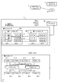
- FIG. 1 is a hardware configuration diagram of a computing system according to one embodiment of the present invention.
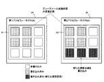
- FIG. 2 is a configuration diagram of the first accelerator and the second accelerator.
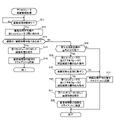
- FIG. 3 is a flowchart of accelerator control management processing.
- FIG. 4 is a configuration diagram of the first accelerator and the second accelerator.
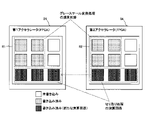
- FIG. 5 is a configuration diagram of the first accelerator and the second accelerator.
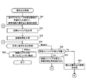
- FIG. 6 is a flowchart of write processing.
- FIG. 7 is a configuration diagram showing how the write area of the second area of the second accelerator is changed.
- FIG. 8 is a hardware configuration diagram of a computing system according to a modification of FIG.
- the computing system 10 includes a first computer 20, a second computer 30, and a first computer communicably connected to the computers 20 and 30 via a LAN (Local Area Network) (not shown) or the like.
- a gateway 40 as a computer.
- the gateway 40 is connected to a network N such as the Internet.
- the gateway 40 relays data, such as images here, exchanged between the computers 20 and 30 and the client computer C of the user using the computing system 10 connected to the network N.
- the computers 20 to 40 operate as computer network nodes that perform various processes in response to requests from each of a plurality of client computers C.
- each client computer C transmits an image to the computing system 10 and requests image processing for the image.
- the computing system 10 performs image processing on the transmitted image, and returns the image after the image processing to the client computer C that transmitted the image.
- Image processing is primarily performed by the first computer 20, as will be described later.
- the first computer 20 includes a CPU (Central Processing Unit) 21, a RAM 22 such as a DRAM (Dynamic Random Access Memory) functioning as the main memory of the CPU 21, and a non-volatile storage device 23.
- the first computer 20 further comprises a first accelerator 24 consisting of an FPGA (Field Programmable Gate Array) and a NIC (Network Interface Card) 25 which is a network card.
- the storage device 23 is an auxiliary storage device such as a hard disk or SSD (Solid State Drive).
- the CPU 21 exchanges data with a gateway or the like outside the first computer 20 , this exchange is performed via the NIC 25 .
- the CPU 21 executes a program stored in the storage device 23 and read out to the RAM 22 to perform the processing described later.
- the second computer 30 is configured by the same computer as the first computer 20 (programs and the like are different). As shown in FIG. 2, the second computer 30 includes a CPU 31, a RAM 32, a storage device 33, a second accelerator 34, and a NIC35.
- SYS-4028GR-TR2 server manufactured by Super Micro Computer
- the CPU motherboard of this server is equipped with two E5-2600V4 Intel Xeon (registered trademark) CPU processors as CPUs, and DDR4-2400 DIMMs manufactured by I-O Data Equipment Co., Ltd. as RAM. Eight 32GB memory cards are installed.
- a PCI Express 3.0 (Gen3) 16-lane slot daughter board is mounted on the CPU motherboard, and this slot is equipped with one ALVEO U250 made by Xillinx as an accelerator, and a NIC made by Mellanox Technologies. ConnectX-4 VPI MCX455A-ECAT is installed.
- the first computer 20 executes multiple types of image processing. A part of the plural types of executable image processing is performed by the CPU 21 executing an image processing program stored in the storage device 23 . The rest of the plurality of types of image processing executable by the first computer 20 are written in the reconfigurable first area of the first accelerator 24 and executed by the arithmetic circuit configured in the first area. . An arithmetic circuit is written in the first area by the CPU 21 applying a circuit config (bitstream file) representing the arithmetic circuit stored in the storage device 23 to a part of the first area.
- a circuit config bitstream file
- one of the image processing performed by the CPU 21 executing the image processing program stored in the storage device 23 is a pixel sorting process for sorting each pixel of an image.
- the image processing executed by the arithmetic circuit is assumed to be grayscale conversion processing for converting an image after pixel sorting into a grayscale image.
- the second accelerator 34 of the second computer 30 has a reconfigurable second area with the same circuit arrangement (same arrangement of switch cells, LUT (Look Up Table), and wiring) as the first area of the first accelerator 24. have.
- the same arithmetic circuit is written in the same position as the first accelerator 24 in the second area.
- the storage device 33 stores a circuit configuration similar to that of the first computer 20 .
- the CPU 21 of the first computer 20 notifies the gateway 40 of the type of arithmetic circuit written to the first accelerator 24 and the writing position in the first area.
- the gateway 40 notifies the second computer 30 of the arithmetic circuit type and writing position notified from the first computer 20 .
- the CPU 31 of the second computer 30 applies the same circuit configuration to the second area of the second accelerator 34 and writes the same arithmetic circuit to the same position. In this way, the arithmetic circuits reconfigured in the first area and the second area are the same. As will be described later, when the same arithmetic circuit has already been written in the same position in the second accelerator 34, the writing of the arithmetic circuit in the second computer 30 is not performed.
- a plurality of types of circuit configurations are registered in the storage devices 33 and 43, and here, one of them, a circuit configuration representing an arithmetic circuit that executes grayscale conversion processing, is applied to each of the accelerators 24 and 34.
- each of the first region R1 and the second region R2 of each accelerator 24 and 34 has nine blocks of 3 ⁇ 3.
- four blocks on the upper left side are used to write arithmetic circuits for executing gray scale conversion processing.
- blocks with dots have been written with an arithmetic circuit
- white blocks have not been written with an arithmetic circuit.
- the gateway 40 consists of a server computer, etc., and includes a CPU, a main memory, a non-volatile storage device, a NIC, etc. (not shown).
- the gateway 40 executes acceleration rate control management processing shown in FIG.
- the gateway 40 first waits until an image processing request containing an image and designation information designating the type of image processing for processing the image is received from one of the plurality of client computers C. (Step S11). If there is reception, the gateway 40 inquires of the first computer 20 whether the type of image processing specified by the specified information is possible (step S12). The first computer 20 determines whether the requested image processing can be performed. Assuming that the designation information of the image processing request is pixel sort processing and gray scale processing, the CPU 21 of the first computer 20 determines that the image processing requested for the image processing request can be performed, and replies to that effect to the gateway 40. do.
- step S13 If there is a reply to the effect that the image processing of the image processing request is possible (step S13; Yes), the gateway 40 supplies the image included in the image processing request to the first computer 20, and receives a reply that the image processing is possible. Execution of image processing is instructed (step S14). In this case, the CPU 21 performs pixel sorting on the received image by executing the program, and performs grayscale conversion on the sorted image by the arithmetic circuit. After that, the CPU 21 returns the grayscale-converted image to the gateway 40 . The gateway 40 returns the returned image to the client computer C, which is the source of the image processing request, via the network N (step S15).
- the CPU 21 of the first computer 20 replies to the gateway 40 that the processing cannot be performed.
- the gateway 40 receives this reply (step S13; No)
- it determines whether a new arithmetic circuit for executing image processing requested for image processing can be written in the first accelerator 24 of the first computer 20 (step S16).
- the gateway 40 determines whether or not the circuit configuration representing the arithmetic circuit that performs the cutting process is stored in the storage device 23 of the first computer 20 . Further, the gateway 40 determines whether the unwritten area of the first area R1 of the first accelerator 24 includes an area in which this arithmetic circuit can be written.
- step S16 If it is not possible to write a new arithmetic circuit, that is, if at least one of the above two determination results is negative (step S16; No), the gateway 40 notifies that processing is not possible when sending the current image processing request. A reply is sent to the original client computer C (step S17).
- the gateway 40 sends the second computer 30 the type specified by the image processing request specification information. (step S18).
- the CPU 31 of the second computer 30 reads out the circuit configuration representing the arithmetic circuit for this cutting process from the storage device 33, and applies the read circuit configuration to the unwritten area of the second accelerator 34. An arithmetic circuit is written in this area (see FIG. 4). The write position is specified by gateway 40 .
- the CPU 31 executes a predetermined program, operates as a test data generating section that generates test data for the arithmetic circuit, inputs the test data to the arithmetic circuit, causes the arithmetic circuit to perform a test operation, Check the normality of this arithmetic circuit.
- the test data generation unit may be configured by the outside of the second computer 30, for example, the CPU within the gateway 40, or the like. When the arithmetic circuit operates normally or does not operate, the CPU 31 notifies the gateway 40 to that effect.
- the gateway 40 performs the type of image processing specified by the specified information of the image processing request, that is, cuts the moving image source.
- a write instruction to the first accelerator 24 of the arithmetic circuit is issued to the first computer 20 (step S20). Further, the gateway 40 transmits to the first computer 20 the image included in the image processing request and an instruction for image processing in the new arithmetic circuit (step S21).
- the CPU 21 of the first computer 20 applies the circuit configuration to the first accelerator 24 according to the write command, writes the arithmetic circuit (see FIG. 5), inputs the image to the arithmetic circuit, and the arithmetic circuit Acquire the image after image processing to be output.
- the CPU 21 returns the acquired image to the gateway 40 .
- the gateway 40 returns the returned image to the client computer C, which is the source of the image processing request, via the network N (step S22).
- step S19 If there is a notification to the effect that the arithmetic circuit does not operate normally (step S19; No), the gateway 40 returns a message to the effect that processing is impossible to the client computer C that has sent the current image processing request (step S17). .
- this arithmetic circuit when a new arithmetic circuit is written in the second region R2, this arithmetic circuit is operated. Then, when this arithmetic circuit operates normally, this arithmetic circuit is written into the first accelerator 24 of the first computer 20 assuming that this arithmetic circuit has been normally written into the second region R2. As a result, for example, the user A requests the computing system 10 to perform pixel sorting processing and grayscale conversion processing. Even when a request is made, the arithmetic circuit is preferably written.
- the operation for testing a new arithmetic circuit or the like may be performed by the second accelerator 34 of the second computer 30. Therefore, the influence of the test operation on the first accelerator 24 and the first computer 20 (such as influence on traffic) can be suppressed. Therefore, a new arithmetic circuit can be introduced into the first accelerator 24 while ensuring the reliability of the first computer 20 . As a result, it is possible to solve the conventional inconvenience such as the decrease in reliability of the first computer 20 when a new arithmetic circuit is introduced. It should be noted that the new arithmetic circuit may be normally written to the second region R2 at the time when the arithmetic circuit can be written to the second accelerator 34 without any abnormality without performing the operation for the test.
- the arithmetic circuit written in the first region R1 of the first accelerator 24 and the arithmetic circuit written in the second region R2 of the second accelerator 34 are separated from each other, including the write position.
- the written portion and the unwritten portion may be located at the same position, and a dummy circuit may be written in the second region R2.
- the arithmetic circuit written in the first region R1 of the first accelerator 24 and the arithmetic circuit written in the second region R2 of the second accelerator 34 are the same including the writing position. Better.
- the already written arithmetic circuit and the newly written arithmetic circuit can be tested in parallel. Then, in the second computer 30, the newly written arithmetic circuit and other arithmetic circuits are tested in parallel, and only when there is no abnormality in each test operation, the new arithmetic circuit is transferred to the first accelerator 24. may be written. As a result, a new arithmetic circuit can be written into the first accelerator 24 without adversely affecting existing arithmetic circuits.
- step S13 In the case where the reply in step S13 indicates that image processing is not possible (step S13; No), when the gateway 40 notifies the client computer C to that effect, the client computer C performs the image processing.
- a write instruction to newly generate and write a config may be supplied to the gateway 40 via the network N.
- FIG. The instruction is supplied to the gateway 40 together with a program for generating the circuit config of the arithmetic circuit. This program may include a hardware description language that is the source of the circuit configuration.
- the gateway 40 executes the write processing shown in FIG. 6 together with the second computer 30 .
- the gateway 40 first secures a write area for writing a new arithmetic circuit in an unwritten portion of the second area R2 of the second accelerator 34 of the second computer 30 (step S51). This reservation prevents another circuit from being written in the write area.
- the size of the write area is specified from the scale of the program (hardware description language, etc.) supplied together with the write instruction.
- the portion indicated by the dotted line in FIG. 7 is reserved as the write area. It is located at the same position as the unwritten portion of the first region R1 of the first accelerator 24 of the first computer 20 .
- the gateway 40 preferably secures an input/output terminal located at the same position as an unused input/output terminal of the first accelerator 24 as an input/output terminal of the secured write area. If the write area could not be secured, the gateway 40 replies to the client computer C to that effect.
- the gateway 40 supplies the program supplied together with the write instruction to the second computer 30, and the CPU 31 of the second computer 30 executes the supplied program, and performs arithmetic circuit processing in the write area secured in step S51. is generated (step S52).
- Generation of the circuit configuration appropriately includes processes such as logic synthesis, placement and routing of the hardware description language included in the program.
- the CPU 31 applies the generated circuit configuration to the currently secured write area, and writes the arithmetic circuit in the area (step S53, see FIG. 4).
- the CPU 31 of the second computer 30 operates the arithmetic circuit written in step S53 to test whether this arithmetic circuit operates normally (step S54).
- the CPU 31 inputs a test pattern (test data) into the arithmetic circuit and operates it to test whether it operates normally.
- test data test data
- the frame loss occurrence probability is higher than a predetermined standard, or when an operation different from the normal operation scenario is performed, for example, when the content of the response to the specified request input to the arithmetic circuit is different
- the criterion for determining whether or not the device is operating normally is determined in advance. This enables efficient judgment.
- the test pattern may be generated by the CPU 31 of the second computer 30 operating as a test pattern generation device that generates test patterns, or may be obtained from a test pattern generation device connected to the second computer 30 .
- the test pattern may be supplied to the second computer 30 via the gateway 40 along with write instructions.
- An FPGA may be used to generate the test pattern. Thereby, a high-load test pattern is easily generated.
- the CPU 31 determines whether or not the arithmetic circuit can be corrected (step S55). If correction is possible (step S55; Yes), the CPU 31 corrects the circuit configuration, applies the corrected circuit configuration to the second region R2, and places the corrected arithmetic circuit in the same position in the second region R2. Write (step S56). If the arithmetic circuit is modifiable, the CPU 31 may transmit to the client computer C via the gateway 40 or the like that the arithmetic circuit needs to be modified. Modification of the circuit configuration may be modification of the original program for generating the circuit configuration and generation of the circuit configuration based on the modified program. Modification of the circuit configuration may be modification of the hardware description language, and logic synthesis and placement and routing based on the modified hardware description language.
- step S55 If it is difficult to modify the arithmetic circuit (step S55; No), the CPU 31 secures another unwritten portion in the second area as a new write area (step S57; see, for example, FIG. 7), and after step S52 process.
- step S54 When there is no abnormality in the operation of the arithmetic circuit (step S54; Yes), the CPU 31 transfers the circuit configuration of the arithmetic circuit together with the writing position of the arithmetic circuit to the first computer 20 via the gateway 40 (step S58). ). The first computer 20 applies the transferred circuit configuration to the first accelerator 24, and writes the normal arithmetic circuit to the write position.
- the arithmetic circuit to be originally written to the first accelerator 24 of the first computer 20 is once written into the second accelerator 34 of the second computer 30, and the operation of this arithmetic circuit is confirmed (here, the above test pattern test), this arithmetic circuit is written into the first accelerator 24 . Therefore, even if processing in the first accelerator 24 of the first computer 20 or other processing for executing a program by the CPU 21 of the first computer 20 is already being executed at the start of the writing process of the arithmetic circuit, the writing of the arithmetic circuit can be suppressed from affecting the processing of the first accelerator 24 or the processing of the CPU 21 of the first computer 20, and a highly reliable computing system 10 is realized. Furthermore, in the above, since logic synthesis and the like are executed on the second computer 30 side, there is no need to perform logic synthesis and the like on the first computer 20, and the processing load on the first computer 20 is reduced.
- FIG. 8 is a diagram focusing on the accelerator, and the CPU and the like are omitted.
- the first computer 20 comprises a 1-1 computer 20A and a 1-2 computer 20B.
- the 1-1 computer 20A comprises a plurality of accelerators 24-1 and 24-2.
- the 1-2nd computer 20B comprises a plurality of accelerators 24-3 and 24-4.
- the 1-1 computer 20A and the 1-2 computer 20B are connected by a network such as a LAN (not shown) or the Internet, and the accelerators 24-1 to 24-4 are a total of one first accelerator 24. It's becoming
- the second computer 30 comprises N (here, eight) accelerators 34-1 to 34-N.
- Buses A1 through An connect accelerators 34-1 through 34-N such that accelerators 34-1 through 34-N form a chain.
- Buses B1 through Bn connect accelerators 34-1 through 34-N to form the origin (input) and endpoint (output) of the chain.
- the accelerators 34-1 to 34-N are a single second accelerator 34 as a whole, simulating a chain path to be described later.
- the first accelerator 24 consisting of accelerators 24-1 to 24-4 and the second accelerator 34 consisting of accelerators 34-1 to 34-N are reconfigurable first and second regions having the same circuit layout as a whole. can be regarded as having each.
- the arithmetic circuit X1 of the accelerator 24-1 preprocesses the image to be processed.
- the arithmetic circuit X2 infers image contents based on the image preprocessed by the arithmetic circuit X1.
- the arithmetic circuits X1 and X2 have a chain configuration. In this state, only processing by the arithmetic circuits X1 and X2 is being executed, and the 1-1 computer 20A is in operation.
- client computer C operated by user B requests gateway 40 for new image processing. If the requested image processing can be performed by the first computer 20, the gateway 40 sets the communication destination of the client computer C to the first computer 20. However, since the current image processing is new processing, the first computer 20 cannot run. At this time, the gateway 40 switches the communication destination of the client computer C to the second computer 30 . At this time, the client computer C of the user B supplies the second computer 30 with a program for generating a circuit configuration representing an arithmetic circuit for image processing requested by the user B.
- the CPU 31 of the second computer 30 determines from the contents of the program from the client computer C that the processing amount of preprocessing is smaller than the processing amount of inference. From this estimation, in the unwritten portion of the first computer 20, for example, the written area Y1 in FIG. is tentatively set as a writing area for writing. The written and unwritten portions of the first accelerator 24 and the second accelerator 34 are shared. Based on the temporary setting result, the CPU 31 writes the arithmetic circuit of the user B in the corresponding areas of the unwritten areas Y1 and Y2 of the second accelerator 34 .
- the buses A1 to An as a whole are buses configured with one optical transmission line and a plurality of optical filters.
- the buses B1 to Bn may also be buses composed of one optical transmission line and a plurality of optical filters.
- optical wavelength multiplexing communication using a plurality of different optical wavelengths is performed.
- a plurality of accelerators may be connected to one transmission line so that each pair of accelerators that communicate with each other can communicate with light of different wavelengths. According to this configuration, there is no need to assign an ID for distribution such as an electric switch to various buses in the chain between connections, so there is an advantage that delay can be reduced.
- the hardware configuration of the computing system 10 is arbitrary.
- at least two of the first computer 20, the second computer 30 and the gateway 40 may be implemented by the same computer.
- the CPU 21 of the first computer 20 may function as the gateway 40 and execute processing of the gateway 40 .
- the processing performed by the first computer 20 and the second computer 30 is not limited to image processing, and may be other processing.
- the first accelerator 24 may also comprise multiple accelerators interconnected in the same manner as the second accelerator 34 of FIG. This allows the first accelerator 24 to simulate the path of the chain.
Landscapes
- Engineering & Computer Science (AREA)
- Theoretical Computer Science (AREA)
- Physics & Mathematics (AREA)
- General Physics & Mathematics (AREA)
- General Engineering & Computer Science (AREA)
- Computational Mathematics (AREA)
- Computing Systems (AREA)
- Mathematical Analysis (AREA)
- Mathematical Optimization (AREA)
- Pure & Applied Mathematics (AREA)
- Quality & Reliability (AREA)
- Hardware Redundancy (AREA)
Abstract
コンピューティングシステム(10)は、第1アクセラレータ(24)が備える再構成可能な第1領域に演算回路を書き込む第1コンピュータ(20)と、第1アクセラレータ(24)とは異なる第2アクセラレータ(34)が備える、再構成可能で第1領域と同じ回路配置の第2領域に演算回路を書き込む第2コンピュータ(30)と、を備える。第2コンピュータ(30)は、第1コンピュータ(20)が第1領域に新たな演算回路を書き込む際に、第2領域のうち、第1領域の未書き込みの部分領域と同じ位置の部分領域に新たな演算回路を書き込む。第1コンピュータ(20)は、前記新たな演算回路が正常に書き込まれないときに、第1領域に前記新たな演算回路を書き込まず、前記新たな演算回路が正常に書き込まれたときに、第1領域の前記未書き込みの部分領域に前記新たな演算回路を書き込む。これにより、演算回路を書き込んだときに書き込み先のアクセラレータが正常に動作しないといった不都合を生じ難くすることができる。
Description
本発明は、コンピューティングシステムに関する。
近年、コンピュータが行う処理の一部を、CPUではなく、回路を再構成可能なアクセラレータに実行させることで、処理の高速化を図り、インターネット上での仮想現実又は人工知能などを実現する技術が開発されている。このような技術を開示する特許文献1には、コンピュータのFPGAアクセラレータに書き込まれる回路を、当該FPGAアクセラレータにより実行させる処理に応じて適宜書き換える技術が開示されている。
上記特許文献1に記載の技術では、新たな演算回路がこのFPGAアクセラレータに直接書き込まれるため、新たな演算回路がこのFPGAアクセラレータに正常に書き込まれなかった場合、FPGAアクセラレータが正常に動作しないといった不都合が生じ得る。
本発明は、演算回路を書き込んだときに書き込み先のアクセラレータが正常に動作しないといった不都合を生じ難くすることを目的とする。
上述した課題を解決するために、本発明に係るコンピューティングシステムは、第1アクセラレータが備える再構成可能な第1領域に演算回路を書き込むように構成された第1コンピュータと、前記第1アクセラレータとは異なる第2アクセラレータが備える、再構成可能で前記第1領域と同じ回路配置の第2領域に演算回路を書き込むように構成された第2コンピュータと、を備え、前記第2コンピュータは、前記第1コンピュータが前記第1領域に新たな演算回路を書き込む際に、前記第2領域のうち、前記第1領域の未書き込みの部分領域と同じ位置の部分領域に新たな演算回路を書き込むように構成されており、前記第1コンピュータは、前記新たな演算回路が正常に書き込まれないときに、前記第1領域に前記新たな演算回路を書き込まず、前記新たな演算回路が正常に書き込まれたときに、前記第1領域の前記未書き込みの部分領域に前記新たな演算回路を書き込む、ように構成されている。
本発明によれば、演算回路を書き込んだときに書き込み先のアクセラレータが正常に動作しないといった不都合を生じ難くすることができる。
以下、本発明の実施の形態に係るコンピューティングシステム10等を、図面を参照して説明する。
図1に示すように、コンピューティングシステム10は、第1コンピュータ20と、第2コンピュータ30と、コンピュータ20及び30と不図示のLAN(Local Area Network)などを介して通信可能に接続された第3コンピュータとしてのゲートウェイ40と、を備える。ゲートウェイ40は、インターネット等のネットワークNに接続されている。ゲートウェイ40は、コンピュータ20及び30と、ネットワークNに接続された、コンピューティングシステム10を利用するユーザのクライアントコンピュータCと、の間でやり取りされるデータ、ここでは画像などを中継する。
コンピュータ20~40は、複数のクライアントコンピュータCそれぞれからの依頼に対して各種処理を行うコンピュータネットワークのノードとして動作する。ここでは、各クライアントコンピュータCは、コンピューティングシステム10に画像を送信し、当該画像に対する画像処理を依頼するものとする。コンピューティングシステム10は、送信されてきた画像に対して画像処理を行って、画像処理後の画像を、画像の送信元のクライアントコンピュータCに返信する。後述のように、画像処理は、主に第1コンピュータ20により行われる。
第1コンピュータ20は、CPU(Central Processing Unit)21、CPU21のメインメモリとして機能するDRAM(Dynamic Random Access Memory)などのRAM22、及び、不揮発性の記憶装置23を備える。第1コンピュータ20は、さらに、FPGA(Field Programmable Gate Array)からなる第1アクセラレータ24、及び、ネットワークカードであるNIC(Network Interface Card)25を備える。記憶装置23は、ハードディスク、又はSSD(Solid State Drive)などの補助記憶装置である。CPU21が第1コンピュータ20外部のゲートウェイなどとデータをやり取りする場合、このやり取りはNIC25経由で行われる。CPU21は、記憶装置23に記憶され、RAM22に読み出されたプログラムを実行することで後述の処理を行う。
第2コンピュータ30は、第1コンピュータ20と同じコンピュータにより構成されている(プログラム等は異なる)。図2に示すように、第2コンピュータ30は、CPU31、RAM32、記憶装置33、第2アクセラレータ34、及び、NIC35を備える。
各コンピュータ20及び30としては、例えば、Super Micro Computer社製のSYS-4028GR-TR2サーバが採用される。このサーバのCPUマザーボードには、CPUとして、Intel社製のXeon(登録商標)CPUプロセッサのE5-2600V4が2台搭載されており、RAMとして、アイ・オー・データ機器社製のDDR4-2400 DIMM 32GBのメモリカードが8枚搭載されている。また、CPUマザーボードにはPCIExpress 3.0 (Gen3)の16レーンスロットのドーターボードが実装され、このスロットに、アクセラレータとして、Xillinx社製のALVEO U250が1台搭載され、NICとして、Mellanox Technologies社製のConnectX-4 VPI MCX455A-ECATが1枚搭載されている。
第1コンピュータ20では、複数種類の画像処理が実行される。実行可能な複数種類の画像処理のうちの一部は、CPU21が記憶装置23に記憶された画像処理プログラムを実行することで行われる。第1コンピュータ20により実行可能な複数種類の画像処理のうちの残りは、第1アクセラレータ24の再構成可能な第1領域に書き込まれることで当該第1領域に構成された演算回路により実行される。演算回路は、CPU21が、記憶装置23に記憶された当該演算回路を表す回路コンフィグ(ビットストリームファイル)を第1領域の一部に適用することにより、当該第1領域に書き込まれる。
ここでは、CPU21が記憶装置23に記憶された画像処理プログラムを実行することで行われる画像処理の1つを、画像の各ピクセルをソートするピクセルソート処理であるとする。さらに、演算回路により実行される画像処理を、ピクセルソート後の画像をグレースケール画像に変換するクレースケール変換処理とする。
第2コンピュータ30の第2アクセラレータ34は、第1アクセラレータ24の第1領域と同じ回路配置(スイッチセル、LUT(Look Up Table)、及び、配線が同じ配置)の再構成可能な第2領域を有する。第2領域には、第1アクセラレータ24と同じ位置に同じ演算回路が書き込まれる。具体的に、記憶装置33には、第1コンピュータ20と同様の回路コンフィグが記憶されている。第1コンピュータ20のCPU21は、第1アクセラレータ24に書き込んだ演算回路の種類及び第1領域における書き込み位置を、ゲートウェイ40に通知する。ゲートウェイ40は、第1コンピュータ20から通知された演算回路の種類及び書き込み位置を第2コンピュータ30に通知する。第2コンピュータ30のCPU31は、この通知に基づいて、同じ回路コンフィグを第2アクセラレータ34の第2領域に適用し、同じ演算回路を同じ位置に書き込む。このようにして、第1領域と第2領域で再構成される演算回路が同じとなっている。なお、後述のように、第2アクセラレータ34にすでに同じ演算回路が同じ位置に書き込まれている場合、第2コンピュータ30での演算回路の書き込みは行われない。
記憶装置33及び43には、複数種類の回路コンフィグが登録されており、ここでは、その1つであるグレースケール変換処理を実行する演算回路を表す回路コンフィグが、各アクセラレータ24及び34に適用されているものとする。記憶装置33及び43に登録されている回路コンフィグは、ゲートウェイ40にも登録されている。つまり、ゲートウェイ40は、各アクセラレータ24及び34に書き込むことができる演算回路の種類を把握している。また、ゲートウェイ40は、第1コンピュータ20のCPU21からの上記通知に基づいて、領域R1及びR2の書き込み済み領域及び未書き込み領域を把握しているものとする。
ここでは、図2に示すように、各アクセラレータ24及び34の第1領域R1及び第2領域R2のそれぞれが、3×3の9つのブロックを有するものとする。そして、第1領域R1及び第2領域R2のそれぞれには、左上側の4つのブロックを使って、クレースケール変換処理を実行する演算回路が書き込まれているものとする。つまり、図2において、ドットが付されたブロックは、演算回路が書き込み済みで、白色のブロックは、演算回路が未書き込みである。
ゲートウェイ40は、サーバコンピュータなどからなり、CPU、メインメモリ、不揮発性の記憶装置、及び、NICなどを備える(図示略)。ゲートウェイ40は、図3に示すアクセラレート制御管理処理を実行する。
図3に示す処理において、ゲートウェイ40は、まず、画像とこの画像を処理する画像処理の種類を指定する指定情報とを含む画像処理依頼を複数のクライアントコンピュータCのいずれかから受信するまで待機する(ステップS11)。受信有りの場合、ゲートウェイ40は、指定情報により指定される種類の画像処理が可能であるかを第1コンピュータ20に問い合わせる(ステップS12)。第1コンピュータ20は、問い合わせを受けた画像処理を行うことが可能であるか判別する。画像処理依頼の指定情報が、ピクセルソート処理及びグレースケール処理であるとすると、第1コンピュータ20のCPU21は、画像処理依頼の画像処理を行うことができると判別し、その旨をゲートウェイ40に返信する。
画像処理依頼の画像処理が可能である旨の返信があった場合(ステップS13;Yes)、ゲートウェイ40は、画像処理依頼に含まれる画像を第1コンピュータ20に供給し、可能との返信があった画像処理の実行を指示する(ステップS14)。この場合、CPU21は、受信した画像に対して、プログラムの実行により、ピクセルソートを行い、演算回路により、ソート後の画像に対してグレースケール変換する。その後、CPU21は、グレースケール変換した画像をゲートウェイ40に返信する。ゲートウェイ40は、返信されてきた画像を、ネットワークNを介して、画像処理依頼の依頼元のクライアントコンピュータCに返信する(ステップS15)。
画像処理依頼の指定情報が、ピクセルソート処理及グレースケール処理以外の例えば、動画ソースの切り取り処理であるとすると、第1コンピュータ20のCPU21は、当該処理を行うことができないとゲートウェイ40に返信する。ゲートウェイ40は、この返信があったとき(ステップS13;No)、第1コンピュータ20の第1アクセラレータ24に、画像処理依頼の画像処理を実行する新たな演算回路を書き込めるかを判別する(ステップS16)。ゲートウェイ40は、この判別において、切り取り処理を行う演算回路を表す回路コンフィグが第1コンピュータ20の記憶装置23に記憶されているかを判別する。さらに、ゲートウェイ40は、第1アクセラレータ24の第1領域R1の未書き込み領域がこの演算回路を書き込み可能な領域を含むかを判別する。
新たな演算回路の書き込みが不可の場合、つまり、前記2つの判別の結果の少なくとも一方が否定の場合(ステップS16;No)、ゲートウェイ40は、処理不可の旨を、今回の画像処理依頼の送信元のクライアントコンピュータCに返信する(ステップS17)。
2つの判別結果の両者が肯定の場合(回路コンフィグが記憶装置23に記憶され、演算回路が書き込み可能の場合)、ゲートウェイ40は、第2コンピュータ30に、画像処理依頼の指定情報が指定する種類の画像処理、つまり、動画ソースの切り取り処理を行う演算回路の書き込み指令を行う(ステップS18)。この指令があったとき、第2コンピュータ30のCPU31は、この切り取り処理の演算回路を表す回路コンフィグを記憶装置33から読み出し、読み出した回路コンフィグを第2アクセラレータ34の未書き込み領域に適用することでこの領域に演算回路を書き込む(図4参照)。書き込み位置は、ゲートウェイ40により指定される。その後、CPU31は、所定のプログラムを実行して、この演算回路用のテストデータを生成するテストデータ生成部として動作し、当該テストデータを演算回路に入力して、この演算回路を試験動作させ、この演算回路の正常性を確認する。なお、テストデータ生成部は、第2コンピュータ30の外部、例えば、ゲートウェイ40内のCPUなどにより構成されてもよい。CPU31は、演算回路が正常に動作する又は動作しない場合、その旨をゲートウェイ40に通知する。
演算回路が正常に動作する旨の通知があった場合(ステップS19;Yes)、ゲートウェイ40は、上記の画像処理依頼の指定情報が指定する種類の画像処理、つまり、動画ソースの切り取り処理を行う演算回路の第1アクセラレータ24への書き込み指令を第1コンピュータ20に対して行う(ステップS20)。さらにゲートウェイ40は、当該画像処理依頼に含まれる画像、及び、新たな演算回路での画像処理の指示を第1コンピュータ20に送信する(ステップS21)。第1コンピュータ20のCPU21は、前記の書き込み指令により、回路コンフィグを第1アクセラレータ24に適用して演算回路を書き込み(図5参照)、かつ、画像を、当該演算回路に入力し、演算回路が出力する画像処理後の画像を取得する。CPU21は、取得した画像をゲートウェイ40に返信する。ゲートウェイ40は、返信されてきた画像を、ネットワークNを介して、画像処理依頼の依頼元のクライアントコンピュータCに返信する(ステップS22)。
演算回路が正常に動作しない旨の通知があった場合(ステップS19;No)、ゲートウェイ40は、処理不可の旨を、今回の画像処理依頼の送信元のクライアントコンピュータCに返信する(ステップS17)。
以上のような一連の処理により、クライアントコンピュータCから依頼された画像処理を行う演算回路が、第1コンピュータ20の第1アクセラレータ24に書き込まれていない場合には、この演算回路を第1アクセラレータ24に書き込む。この書き込みの際、まず、第2コンピュータ30が、第2領域R2のうち、第1領域R1の未書き込みの部分領域と同じ位置の部分領域に新たな演算回路を書き込む。そして、第1コンピュータ20は、第2領域R2に前記新たな演算回路が正常に書き込まれたときにのみ、第1領域R1の前記未書き込みの部分領域にこの新たな演算回路を書き込む。これにより、第1アクセラレータ24に演算回路が正常に書き込まれる可能性が高く、第1アクセラレータ24に演算回路を直接書き込んだときに演算回路が正常に書き込まれずに第1アクセラレータ24が正常に動作しないといった不都合が生じ難くなっている。
さらに、上記では、第2領域R2に新たな演算回路が書き込まれたとき、この演算回路を動作させる。そして、この演算回路が正常に動作したときに、第2領域R2にこの演算回路が正常に書き込まれたとして、第1コンピュータ20の第1アクセラレータ24にこの演算回路が書き込まれる。これにより、例えば、コンピューティングシステム10に対して、ユーザAがピクセルソート処理及びグレースケール変換処理の依頼を行い、ピクセルソート処理及びグレースケール処理の実行中において、ユーザBが動画ソースの切り取り処理の依頼を行ったときであっても、好適に演算回路が書き込まれる。つまり、第1アクセラレータ24が動作中又は第1コンピュータ20のCPU21が他の処理を実行中であっても、新たな演算回路の試験のための動作などが、第2コンピュータ30の第2アクセラレータ34で行われるので、当該試験の動作による第1アクセラレータ24への影響及び第1コンピュータ20への影響(トラヒックへの影響など)を抑制できる。従って、第1コンピュータ20の信頼性を担保しながら新たな演算回路を第1アクセラレータ24に導入できる。これにより、新たな演算回路の導入時における第1コンピュータ20の信頼性の低下といった従来の不都合を解消できる。なお、上記試験のための動作を行わず、演算回路が第2アクセラレータ34に異常なく書き込めた時点で、第2領域R2に前記新たな演算回路が正常に書き込まれたとしてもよい。
上記実施の形態では、図5に示すように、第1アクセラレータ24の第1領域R1に書き込んだ演算回路と、第2アクセラレータ34の第2領域R2に書き込んだ演算回路とを、書き込み位置を含めて同じにしているが、両領域R1及びR2で書き込み済みの部分と、未書き込みの部分とを同じ位置とすればよく、第2領域R2には例えばダミーの回路が書き込まれてもよい。ただし、図5に示すように、第1アクセラレータ24の第1領域R1に書き込んだ演算回路と、第2アクセラレータ34の第2領域R2に書き込んだ演算回路とを、書き込み位置を含めて同じにする方がよい。これにより、第2コンピュータ30において、すでに書き込み済みの演算回路と、新たに書き込んだ演算回路とを並行して試験動作させることができる。そして、第2コンピュータ30において、新たに書き込んだ演算回路と他の演算回路とを並行して試験動作し、各試験動作において異常がないときに限って、第1アクセラレータ24に当該新たな演算回路を書き込んでもよい。これにより、第1アクセラレータ24に、既存の演算回路に悪影響を与えずに新たな演算回路を書き込むことができる。
ステップS13で返信が画像処理不可の旨である場合(ステップS13;No)などにおいて、ゲートウェイ40がその旨をクライアントコンピュータCに通知した場合、クライアントコンピュータCは、その画像処理を行う演算回路の回路コンフィグを新たに生成して書き込む書き込み指示を、ネットワークNを介してゲートウェイ40に供給してもよい。当該指示は、当該演算回路の回路コンフィグを生成するためのプログラムとともにゲートウェイ40に供給される。このプログラムは、回路コンフィグの元となるハードウェア記述言語などを含んでもよい。書き込み指示を受けたゲートウェイ40は、第2コンピュータ30とともに図6に示す書き込み処理を実行する。
図6に示す書き込み処理において、ゲートウェイ40は、まず、第2コンピュータ30の第2アクセラレータ34の第2領域R2の未書き込み部分に、新たな演算回路を書き込む書き込み領域を確保する(ステップS51)。この確保により、当該書き込み領域に別の回路が書き込まれるなどが防止される。書き込み領域の大きさは、書き込み指示とともに供給されるプログラム(ハードウェア記述言語など)の規模から特定される。ここでは、図7の点線で示す部分が書き込み領域として確保されたものとする。第1コンピュータ20の第1アクセラレータ24の第1領域R1の未書き込み部分と同じ位置にある。なお、帯域輻輳による性能劣化を回避するため、ゲートウェイ40は、確保する書き込み領域の入出力端子として、第1アクセラレータ24の未使用の入出力端子と同じ位置にある入出力端子を確保するとよい。書き込み領域が確保できなかった場合、ゲートウェイ40は、その旨をクライアントコンピュータCに返信する。
その後、ゲートウェイ40は、書き込み指示とともに供給されたプログラムを第2コンピュータ30に供給し、第2コンピュータ30のCPU31は、供給されたプログラムを実行して、ステップS51で確保された書き込み領域で演算回路を構成するための回路コンフィグを生成する(ステップS52)。回路コンフィグの生成は、前記プログラムに含まれるハードウェア記述言語の論理合成、配置配線などの処理を適宜含む。その後、CPU31は、生成した回路コンフィグを、現在確保されている書き込み領域に適用して、当該領域に演算回路を書き込む(ステップS53。図4参照)。
その後、第2コンピュータ30のCPU31は、ステップS53で書き込んだ演算回路を動作させて、この演算回路が正常に動作するかどうか試験する(ステップS54)。CPU31は、テストパターン(テストデータ)を演算回路に入力して動作させることで正常に動作するかの試験を行う。前記の試験では、フレームロスの発生確率が所定基準よりも高いとき、又は、正常動作シナリオと異なる動作が行われたとき、例えば、演算回路に入力する規定のリクエストに対する応答の中身が異なったときなどに、演算回路が正常に動作していないと判断される。なお、正常に動作しているか否かの判断基準は、予め定められているとよい。これにより、効率的な判断が可能となる。テストパターンは、テストパターンを生成するテストパターン生成装置として動作する第2コンピュータ30のCPU31により生成されてもよいし、第2コンピュータ30に接続されたテストパターン生成装置から取得してもよい。テストパターンは、書き込み指示とともにゲートウェイ40を介して第2コンピュータ30に供給されてもよい。テストパターンの生成には、FPGAを用いるとよい。これにより、高負荷なテストパターンが容易に生成される。
CPU31は、演算回路の動作に異常がある場合、演算回路の修正が可能であるか否かを判別する(ステップS55)。修正が可能であれば(ステップS55;Yes)、CPU31は、回路コンフィグを修正し、修正した回路コンフィグを第2領域R2に適用して、修正後の演算回路を第2領域R2の同じ位置に書き込む(ステップS56)。CPU31は、演算回路が修正可能である場合、演算回路の修正が必要である旨を、ゲートウェイ40などを介してクライアントコンピュータCに送信してもよい。回路コンフィグの修正は、回路コンフィグを生成するもとのプログラムの修正及び修正したプログラムに基づく回路コンフィグの生成であってもよい。回路コンフィグの修正は、ハードウェア記述言語の修正と、修正後のハードウェア記述言語に基づく論理合成及び配置配線と、であってもよい。
CPU31は、演算回路の修正が困難な場合(ステップS55;No)は、第2領域における他の未書き込み部分を新たな書き込み領域として確保し(ステップS57。例えば、図7参照)、ステップS52以降の処理を行う。
CPU31は、演算回路の動作に異常がなかった場合(ステップS54;Yes)、この演算回路の回路コンフィグを、演算回路の書き込み位置とともに、ゲートウェイ40を介して第1コンピュータ20に転送する(ステップS58)。第1コンピュータ20は、転送されてきた回路コンフィグを第1アクセラレータ24に適用し、上記異常のなかった演算回路を上記書き込み位置に書き込む。
上記一連の処理により、第2コンピュータ30の第2アクセラレータ34に、本来第1コンピュータ20の第1アクセラレータ24に書き込む演算回路が一度書き込まれ、この演算回路の動作確認(ここでは、上記テストパターンにより試験)がなされてから、この演算回路が第1アクセラレータ24に書き込まれる。従って、演算回路の書き込み処理開始時に、すでに第1コンピュータ20の第1アクセラレータ24での処理又は第1コンピュータ20のCPU21によってプログラムを実行する他の処理が実行中であっても、演算回路の書き込みが第1アクセラレータ24の処理又は第1コンピュータ20のCPU21の処理に影響を与えることを抑制でき、信頼性の高いコンピューティングシステム10が実現される。さらに上記では、論理合成などが第2コンピュータ30側で実行されるので、第1コンピュータ20で論理合成などを行う必要がなくなり、第1コンピュータ20の処理負担が軽減される。
コンピューティングシステム10の他の変形例について図8を参照して説明する。なお、図8では、アクセラレータに注目した図であり、CPUなどは省略されている。
第1コンピュータ20は、第1-1コンピュータ20Aと、第1-2コンピュータ20Bと、備える。第1-1コンピュータ20Aは、複数のアクセラレータ24-1及び24-2を備える。第1-2コンピュータ20Bは、複数のアクセラレータ24-3及び24-4を備える。第1-1コンピュータ20Aと第1-2コンピュータ20Bとは、不図示のLAN、インターネットなどのネットワークで接続されており、アクセラレータ24-1~24-4は、全体で1の第1アクセラレータ24となっている。
第2コンピュータ30は、N(ここでは、8つ)個のアクセラレータ34-1~34-Nを備える。アクセラレータ34-1~34-Nは、バスA1~An(n=N*(N-1)/2)により相互接続されている。さらに、アクセラレータ34-1~34-Nは、バスA1~Anとは分離されたバスB1~Bn(n=N*(N-1)/2)により相互接続されている。バスA1~Anは、アクセラレータ34-1~34-Nがチェーンを構成するようにアクセラレータ34-1~34-Nを接続する。バスB1~Bnは、前記チェーンの起点(入力)及び終点(出力)を構成するようにアクセラレータ34-1~34-Nを接続する。これら構成を実現するため、バスA1~An及びバスB1~Bnの一部は、適宜使用されないように遮断されてもよい。このような相互接続により、アクセラレータ34-1~34-Nは、全体で1の第2アクセラレータ34となっており、後述するチェーンの経路を模擬している。
アクセラレータ24-1~24-4からなる第1アクセラレータ24と、アクセラレータ34-1~34-Nからなる第2アクセラレータ34とは、全体で同じ回路配置の再構成可能な第1領域及び第2領域をそれぞれ有するものとみなせる。
次に、この変形例のコンピューティングシステム10の動作について説明する。ここでは、ユーザAにより第1-1コンピュータ20Aの2つのアクセラレータ24-1及び24-2に、演算回路X1及びX2が書き込まれているとする。アクセラレータ24-1の演算回路X1は、処理対象の画像について前処理を行う。演算回路X2は、演算回路X1で前処理した画像を元に、画像内容を推論する。演算回路X1及びX2は、チェーン構成を取っている。この状態で、演算回路X1及びX2による処理のみが実行されており、第1-1コンピュータ20Aは運用中の状態であるとする。
この際に、ユーザBが操作するクライアントコンピュータCから新たな画像処理が、ゲートウェイ40に要求されたとする。要求された画像処理が第1コンピュータ20で行うことができる場合、ゲートウェイ40は、クライアントコンピュータCの通信先を第1コンピュータ20とするが、今回の画像処理は新しい処理であるので、第1コンピュータ20で実行できない。このとき、ゲートウェイ40は、クライアントコンピュータCの通信先を第2コンピュータ30に切り替える。このとき、ユーザBのクライアントコンピュータCは、ユーザBの要求する画像処理の演算回路を表す回路コンフィグを生成するためのプログラムを第2コンピュータ30に供給する。
ユーザBが要求する画像処理は、ユーザAと同様のチェーン処理で、画像の前処理を行ってから、画像の推論処理を行う処理であるとする。第2コンピュータ30のCPU31は、クライアントコンピュータCからのプログラムの内容から、前処理の処理量が、推論の処理量よりも小さいことを判別する。この見積もりから、第1コンピュータ20の未書き込み部分で、例えば、図8の書き込み領域Y1を、画像の前処理を行う演算回路を書き込む書き込み領域とし、未書き込み領域Y2を、前処理後の推論処理を行う演算回路を書き込む書き込み領域とし仮設定する。第1アクセラレータ24と第2アクセラレータ34の各書き込み済み部分及び未書き込み部分は共有されている。CPU31は、前記仮設定の結果をもとに、第2アクセラレータ34の未書き込み領域Y1及びY2の対応する領域に、ユーザBの演算回路を書き込む。書き込み後は、演算回路の正常動作(長期安定動作を含む)が確認される。十分な検査後、書き込み領域Y1及びY2に演算回路が書き込まれ、第2アクセラレータ34の正常動作が可能となる。なお、ユーザBの演算回路とユーザAの演算回路とが第2アクセラレータ34に書き込まれていることで、例えば、システムの運用側が、第1コンピュータ20で実際に使用されるデータを第2コンピュータ30側に転写して第2アクセラレータ34に入力することで、ユーザB側の新たな演算回路の書き込みにより、すでに書き込まれているユーザA側の演算回路の動作に影響があるかを動作確認できる。
ここでは、バスA1~Anは、全体で、1つの光伝送路及び複数の光フィルタで構成されるバスとなっている。同様に、バスB1~Bnも、1つの光伝送路及び複数の光フィルタで構成されるバスとするとよい。バス内では、異なる複数の光波長が使用される光波長多重通信が行われる。このように、複数のアクセラレータ同士は、通信を行うアクセラレータの組それぞれで異なる波長の光で通信可能に、一の伝送路に接続されているとよい。この構成によれば、電気スイッチのような振り分け用のIDを接続間のチェーン内の各種バスに付与しなくても良いので、低遅延化が可能であるというメリットがある。
コンピューティングシステム10のハードウェア構成は任意である。例えば、第1コンピュータ20、第2コンピュータ30、ゲートウェイ40のうちの少なくとも2つは、同じコンピュータにより実現されてもよい。例えば、第1コンピュータ20のCPU21がゲートウェイ40として機能して、ゲートウェイ40の処理を実行してもよい。第1コンピュータ20、第2コンピュータ30が行う処理は、画像処理に限定されず、他の処理であってもよい。第2アクセラレータ34に加え又は代えて第1アクセラレータ24も、図8の第2アクセラレータ34と同様に相互接続された複数のアクセラレータを備えてもよい。これによって第1アクセラレータ24で、チェーンの経路を模擬してもよい。
(本発明の範囲)
以上、実施の形態及び変形例を参照して本発明を説明したが、本発明は、上記の実施の形態及び変形例に限定されるものではない。例えば、本発明には、本発明の技術思想の範囲内で当業者が理解し得る、上記の実施の形態及び変形例に対する様々な変更が含まれる。上記実施の形態及び変形例に挙げた各構成は、矛盾の無い範囲で適宜組み合わせることができる。
以上、実施の形態及び変形例を参照して本発明を説明したが、本発明は、上記の実施の形態及び変形例に限定されるものではない。例えば、本発明には、本発明の技術思想の範囲内で当業者が理解し得る、上記の実施の形態及び変形例に対する様々な変更が含まれる。上記実施の形態及び変形例に挙げた各構成は、矛盾の無い範囲で適宜組み合わせることができる。
10…コンピューティングシステム、20,20A,20B…第1コンピュータ、22…メインメモリ、24…第1アクセラレータ、24-1~4…アクセラレータ、30…第2コンピュータ、34…第2アクセラレータ、34-1~N…アクセラレータ、40…ゲートウェイ、A1~An…バス、B1~Bn…バス、C…クライアントコンピュータ、N…ネットワーク、R1…第1領域、R2…第2領域、X1,X2…演算回路、Y1,Y2…領域。
Claims (7)
- 第1アクセラレータが備える再構成可能な第1領域に演算回路を書き込むように構成された第1コンピュータと、
前記第1アクセラレータとは異なる第2アクセラレータが備える、再構成可能で前記第1領域と同じ回路配置の第2領域に演算回路を書き込むように構成された第2コンピュータと、を備え、
前記第2コンピュータは、前記第1コンピュータが前記第1領域に新たな演算回路を書き込む際に、前記第2領域のうち、前記第1領域の未書き込みの部分領域と同じ位置の部分領域に新たな演算回路を書き込むように構成されており、
前記第1コンピュータは、前記新たな演算回路が正常に書き込まれないときに、前記第1領域に前記新たな演算回路を書き込まず、前記新たな演算回路が正常に書き込まれたときに、前記第1領域の前記未書き込みの部分領域に前記新たな演算回路を書き込む、ように構成されている、
コンピューティングシステム。 - 前記第2コンピュータは、前記新たな演算回路を書き込む際に前記新たな演算回路を動作させ、
前記新たな演算回路が正常に書き込まれたときは、前記演算回路が正常に動作したときを含む、
請求項1に記載のコンピューティングシステム。 - 前記第2コンピュータが前記新たな演算回路を動作させる際に、当該新たな演算回路に入力するテストデータを生成する生成部をさらに備える、
請求項2に記載のコンピューティングシステム。 - 前記第2コンピュータは、前記第1領域と前記第2領域とにおける同じ位置に同じ内容の演算回路が書き込み済みのときに、当該書き込み済みの演算回路と前記新たな演算回路とを並行して試験動作させるように構成され、
前記第1コンピュータは、前記書き込み済みの演算回路と前記新たな演算回路とが正常に試験動作したときに、前記第1アクセラレータの前記未書き込みの部分領域に前記新たな演算回路を書き込むように構成されている、
請求項1から3のいずれか1項に記載のコンピューティングシステム。 - 前記第1コンピュータによる前記第1領域への演算回路の書き込みと、前記第2コンピュータによる前記第2領域への演算回路の書き込みと、を制御する第3コンピュータをさらに備え、
前記第3コンピュータは、
前記第2コンピュータに前記新たな演算回路の書き込みを行わせ、
前記新たな演算回路が正常に書き込まれたときに、前記第1コンピュータに、前記新たな演算回路の書き込みを行わせる、
請求項1から4のいずれか1項に記載のコンピューティングシステム。 - 前記第1アクセラレータと前記第2アクセラレータとのうちの少なくとも一方は、前記第1領域又は第2領域を構成する、相互接続された複数のFPGAアクセラレータを含んで構成されている、
請求項1から5のいずれか1項に記載のコンピューティングシステム。 - 複数のアクセラレータ同士は、通信を行うアクセラレータの組それぞれで異なる波長の光で通信可能に、一の伝送路に接続されている、
請求項6に記載のコンピューティングシステム。
Priority Applications (3)
| Application Number | Priority Date | Filing Date | Title |
|---|---|---|---|
| PCT/JP2021/023377 WO2022269677A1 (ja) | 2021-06-21 | 2021-06-21 | コンピューティングシステム |
| JP2023529208A JP7683695B2 (ja) | 2021-06-21 | 2021-06-21 | コンピューティングシステム |
| US18/569,383 US20240272872A1 (en) | 2021-06-21 | 2021-06-21 | Computing system |
Applications Claiming Priority (1)
| Application Number | Priority Date | Filing Date | Title |
|---|---|---|---|
| PCT/JP2021/023377 WO2022269677A1 (ja) | 2021-06-21 | 2021-06-21 | コンピューティングシステム |
Publications (1)
| Publication Number | Publication Date |
|---|---|
| WO2022269677A1 true WO2022269677A1 (ja) | 2022-12-29 |
Family
ID=84544248
Family Applications (1)
| Application Number | Title | Priority Date | Filing Date |
|---|---|---|---|
| PCT/JP2021/023377 Ceased WO2022269677A1 (ja) | 2021-06-21 | 2021-06-21 | コンピューティングシステム |
Country Status (3)
| Country | Link |
|---|---|
| US (1) | US20240272872A1 (ja) |
| JP (1) | JP7683695B2 (ja) |
| WO (1) | WO2022269677A1 (ja) |
Citations (4)
| Publication number | Priority date | Publication date | Assignee | Title |
|---|---|---|---|---|
| JP2005115566A (ja) * | 2003-10-06 | 2005-04-28 | Murata Mach Ltd | データ処理装置及びデータ処理装置のテスト方法 |
| JP2017045318A (ja) * | 2015-08-27 | 2017-03-02 | 富士ゼロックス株式会社 | 電子機器 |
| JP2017120966A (ja) * | 2015-12-28 | 2017-07-06 | 株式会社リコー | 情報処理装置、情報処理方法およびプログラム |
| JP2018165908A (ja) * | 2017-03-28 | 2018-10-25 | 富士通株式会社 | 情報処理装置、情報処理方法及びプログラム |
-
2021
- 2021-06-21 US US18/569,383 patent/US20240272872A1/en active Pending
- 2021-06-21 WO PCT/JP2021/023377 patent/WO2022269677A1/ja not_active Ceased
- 2021-06-21 JP JP2023529208A patent/JP7683695B2/ja active Active
Patent Citations (4)
| Publication number | Priority date | Publication date | Assignee | Title |
|---|---|---|---|---|
| JP2005115566A (ja) * | 2003-10-06 | 2005-04-28 | Murata Mach Ltd | データ処理装置及びデータ処理装置のテスト方法 |
| JP2017045318A (ja) * | 2015-08-27 | 2017-03-02 | 富士ゼロックス株式会社 | 電子機器 |
| JP2017120966A (ja) * | 2015-12-28 | 2017-07-06 | 株式会社リコー | 情報処理装置、情報処理方法およびプログラム |
| JP2018165908A (ja) * | 2017-03-28 | 2018-10-25 | 富士通株式会社 | 情報処理装置、情報処理方法及びプログラム |
Also Published As
| Publication number | Publication date |
|---|---|
| US20240272872A1 (en) | 2024-08-15 |
| JPWO2022269677A1 (ja) | 2022-12-29 |
| JP7683695B2 (ja) | 2025-05-27 |
Similar Documents
| Publication | Publication Date | Title |
|---|---|---|
| CN108170590B (zh) | 一种区块链系统的测试系统和方法 | |
| US7274706B1 (en) | Methods and systems for processing network data | |
| US20220210019A1 (en) | Management Method and Apparatus | |
| KR102103596B1 (ko) | 계산 작업을 처리하기 위한 컴퓨터 클러스터 장치 및 이를 작동시키기 위한 방법 | |
| US20100064070A1 (en) | Data transfer unit for computer | |
| US12182617B2 (en) | Execution job compute unit composition in computing clusters | |
| US12175292B2 (en) | Job target aliasing in disaggregated computing systems | |
| CN115269174A (zh) | 一种数据传输方法、数据处理方法及相关产品 | |
| CN119027300B (zh) | 一种数据缓存方法、系统、产品、设备及存储介质 | |
| CN115858103B (zh) | 用于开放堆栈架构虚拟机热迁移的方法、设备及介质 | |
| CN115934624B (zh) | 多主机远程直接内存访问网络管理的方法、设备及介质 | |
| CN117519908A (zh) | 一种虚拟机热迁移方法、计算机设备及介质 | |
| US20250209013A1 (en) | Dynamic server rebalancing | |
| JP7683695B2 (ja) | コンピューティングシステム | |
| WO2025190343A1 (zh) | 一种模型训练方法、系统及相关设备 | |
| Jayakumar | Why Use Containers and Cloud-Native Functions Anyway? | |
| US7694064B2 (en) | Multiple cell computer systems and methods | |
| Wang et al. | Container resource allocation versus performance of data-intensive applications on different cloud servers | |
| US11256643B2 (en) | System and method for high configurability high-speed interconnect | |
| WO2023177982A1 (en) | Dynamic server rebalancing | |
| US20200387396A1 (en) | Information processing apparatus and information processing system | |
| JP2009199433A (ja) | ネットワーク処理装置およびネットワーク処理プログラム | |
| CN113992683B (zh) | 实现同一集群中双网络有效隔离的方法、系统、设备及介质 | |
| Sugiarto et al. | Task graph mapping of general purpose applications on a neuromorphic platform | |
| CN115686836B (zh) | 一种安装有加速器的卸载卡 |
Legal Events
| Date | Code | Title | Description |
|---|---|---|---|
| 121 | Ep: the epo has been informed by wipo that ep was designated in this application |
Ref document number: 21946968 Country of ref document: EP Kind code of ref document: A1 |
|
| WWE | Wipo information: entry into national phase |
Ref document number: 2023529208 Country of ref document: JP |
|
| NENP | Non-entry into the national phase |
Ref country code: DE |
|
| 122 | Ep: pct application non-entry in european phase |
Ref document number: 21946968 Country of ref document: EP Kind code of ref document: A1 |